EP4087133A1 - Relaxation oscillator that samples voltage difference between voltages generated by resistor-capacitor charging and discharging for controlling output clock frequency of controllable oscillator and associated relaxation oscillation method - Google Patents

Relaxation oscillator that samples voltage difference between voltages generated by resistor-capacitor charging and discharging for controlling output clock frequency of controllable oscillator and associated relaxation oscillation method Download PDF

Info

Publication number
EP4087133A1
EP4087133A1 EP21218212.5A EP21218212A EP4087133A1 EP 4087133 A1 EP4087133 A1 EP 4087133A1 EP 21218212 A EP21218212 A EP 21218212A EP 4087133 A1 EP4087133 A1 EP 4087133A1
Authority
EP
European Patent Office
Prior art keywords
capacitor
voltage
switch
plate
control signal
Prior art date
Legal status (The legal status is an assumption and is not a legal conclusion. Google has not performed a legal analysis and makes no representation as to the accuracy of the status listed.)
Pending
Application number
EP21218212.5A
Other languages
German (de)
French (fr)
Inventor
Fan-wei LIAO
Current Assignee (The listed assignees may be inaccurate. Google has not performed a legal analysis and makes no representation or warranty as to the accuracy of the list.)
MediaTek Inc
Original Assignee
MediaTek Inc
Priority date (The priority date is an assumption and is not a legal conclusion. Google has not performed a legal analysis and makes no representation as to the accuracy of the date listed.)
Filing date
Publication date
Application filed by MediaTek Inc filed Critical MediaTek Inc
Publication of EP4087133A1 publication Critical patent/EP4087133A1/en
Pending legal-status Critical Current

Links

Images

Classifications

    • HELECTRICITY
    • H03ELECTRONIC CIRCUITRY
    • H03KPULSE TECHNIQUE
    • H03K3/00Circuits for generating electric pulses; Monostable, bistable or multistable circuits
    • H03K3/01Details
    • H03K3/012Modifications of generator to improve response time or to decrease power consumption
    • HELECTRICITY
    • H03ELECTRONIC CIRCUITRY
    • H03KPULSE TECHNIQUE
    • H03K3/00Circuits for generating electric pulses; Monostable, bistable or multistable circuits
    • H03K3/02Generators characterised by the type of circuit or by the means used for producing pulses
    • H03K3/023Generators characterised by the type of circuit or by the means used for producing pulses by the use of differential amplifiers or comparators, with internal or external positive feedback
    • H03K3/0231Astable circuits
    • HELECTRICITY
    • H03ELECTRONIC CIRCUITRY
    • H03BGENERATION OF OSCILLATIONS, DIRECTLY OR BY FREQUENCY-CHANGING, BY CIRCUITS EMPLOYING ACTIVE ELEMENTS WHICH OPERATE IN A NON-SWITCHING MANNER; GENERATION OF NOISE BY SUCH CIRCUITS
    • H03B5/00Generation of oscillations using amplifier with regenerative feedback from output to input
    • H03B5/20Generation of oscillations using amplifier with regenerative feedback from output to input with frequency-determining element comprising resistance and either capacitance or inductance, e.g. phase-shift oscillator
    • GPHYSICS
    • G06COMPUTING OR CALCULATING; COUNTING
    • G06FELECTRIC DIGITAL DATA PROCESSING
    • G06F1/00Details not covered by groups G06F3/00 - G06F13/00 and G06F21/00
    • G06F1/04Generating or distributing clock signals or signals derived directly therefrom

Definitions

  • the present invention relates to an oscillator design, and more particularly, to a relaxation oscillator that samples a voltage difference between voltages generated by resistor-capacitor (RC) charging and discharging for controlling an output clock frequency of a controllable oscillator and an associated relaxation oscillation method.
  • RC resistor-capacitor
  • Typical integrated circuits often include one or more on-chip oscillators to develop clock signals .
  • a relaxation oscillator may be used to generate an output clock with a target frequency.
  • One feature of the relaxation oscillator is that the relaxation oscillator is capable of generating the output clock without the need of a reference clock.
  • a typical relaxation oscillator design may include a plurality of current sources and/or a continuous comparator. However, the continuous comparator is a power-hungry component, and the current source generally has high quiescent current. As a result, the typical relaxation oscillator design may fail to meet requirements of low-power applications. Thus, there is a need for an innovative ultra-low power relaxation oscillator design.
  • One of the objectives of the claimed invention is to provide a relaxation oscillator that samples a voltage difference between voltages generated by resistor-capacitor (RC) charging and discharging for controlling an output clock frequency of a controllable oscillator and an associated relaxation oscillation method.
  • RC resistor-capacitor
  • an exemplary relaxation oscillator includes a resistor-capacitor (RC) circuit, an integration capacitor, a sampling circuit, and a controllable oscillator.
  • the RC circuit is arranged to perform an RC charging operation to set a first voltage, perform an RC discharging operation to set a second voltage, and perform a reset operation to reset the first voltage to a first reference voltage and reset the second voltage to a second reference voltage.
  • the sampling circuit is arranged to perform a charge delivery operation to sample a voltage difference between the first voltage and the second voltage and transfer the voltage difference to the integration capacitor.
  • the controllable oscillator is arranged to generate an output clock in response to a control input provided by the integration capacitor.
  • an exemplary relaxation oscillation method includes: performing a resistor-capacitor (RC) charging operation to set a first voltage; performing an RC discharging operation to set a second voltage; performing a charge delivery operation to sample a voltage difference between the first voltage and the second voltage and transfer the voltage difference to an integration capacitor; in response to a control input provided by the integration capacitor, generating an output clock at a controllable oscillator; and performing a reset operation to reset the first voltage to a first reference voltage and reset the second voltage to a second reference voltage.
  • RC resistor-capacitor
  • FIG. 1 is a block diagram illustrating fundamental architecture of a relaxation oscillator according to an embodiment of the present invention.
  • the relaxation oscillator 100 includes a resistor-capacitor (RC) circuit 102, a sampling circuit 104, an integration capacitor 106, a controllable oscillator 108, and a control signal generator circuit 110.
  • the RC circuit 102 includes resistor (s) and capacitor(s), and is arranged to perform an RC charging operation to set one voltage V CN , perform an RC discharging operation to set another voltage V CP , and perform a reset operation to reset the voltage V CN to one reference voltage such as a ground voltage GND and reset the voltage V CP to another reference voltage such as a supply voltage V DD .
  • the RC circuit 102 may be implemented by a switched RC circuit.
  • the sampling circuit 104 is arranged to perform a charge delivery operation to sample a voltage difference ⁇ V between two voltages V CN and V CP and transfer the voltage difference ⁇ V to the integration capacitor 106.
  • the sampling circuit 104 may be implemented by a unity-gain amplifier for amplifying the direct-current (DC) voltage.
  • the controllable oscillator 108 is arranged to generate an output clock CKOUT in response to a control input (e.g., voltage input V INT ) provided by the integration capacitor 106.
  • controllable oscillator 108 may be implemented by a voltage-controlled oscillator (VCO), and a frequency of the output clock CKOUT is controlled by the voltage input of the VCO.
  • VCO voltage-controlled oscillator
  • the control signal generator circuit 110 is arranged to generate control signals for controlling operation timing of circuit components included in the RC circuit 102 and the sampling circuit 104.
  • the control signal generator circuit 110 may refer to the output clock CKOUT for generating a plurality of clock signals as the control signals, where a frequency of each control signal is lower than a frequency of the output clock CKOUT.
  • the output clock CKOUT is generated from the controllable oscillator 108 with the control input V INT provided by the integration capacitor 106.
  • the RC circuit 102 is used to provide two voltages V CN and V CP from which the voltage difference ⁇ V is sampled for controlling the control input V INT at the integration capacitor 106.
  • no current source with high quiescent current is needed by the proposed relaxation oscillator 100.
  • the switched RC circuit may operate under an RC switching frequency much lower the frequency of the output clock CKOUT. Hence, the power requirement of the switched RC circuit can be relaxed.
  • the control signals generated from the control signal generator circuit 110 may be non-overlapping clock signals used for non-overlapping phase control of the proposed relaxation oscillator 100.
  • the control signal generator circuit 110 can be implemented by a simple logic circuit for power saving.
  • circuit components of the RC circuit 102 and the sampling circuit 104 are active during ON periods (logic high periods) of related control signals generated from the control signal generator circuit 110 and are inactive during OFF periods (logic low periods) of related control signals generated from the control signal generator circuit 110.
  • all circuit components of the RC circuit 102 and the sampling circuit 104 are not always in operation, which results in lower power consumption.
  • the relaxation oscillator 100 employs an ultra-low power relaxation oscillator design. Further details of the relaxation oscillator 100 are described with reference to the accompanying drawings.
  • FIG. 2 is a diagram illustrating a circuit design of a relaxation oscillator according to an embodiment of the present invention.
  • the relaxation oscillator 200 is based on the fundamental architecture of the relaxation oscillator 100 shown in FIG. 1 .
  • the RC circuit 102 shown in FIG. 1 may be implemented by a switched RC circuit 202 shown in FIG. 2
  • the sampling circuit 104 shown in FIG. 1 may be implemented by a unity-gain amplifier 204 shown in FIG. 2
  • the integration capacitor 106 shown in FIG. 1 may be implemented by an integration capacitor C INT shown in FIG. 2
  • the controllable oscillator 108 shown in FIG. 1 may be implemented by a VCO 206 shown in FIG. 2
  • the control signal generator circuit 110 shown in FIG. 1 may be implemented by a phase generator circuit (labeled as "Phase Gen.") 208 shown in FIG. 2 .
  • Phase generator circuit labeleled as "Phase Gen."
  • sampling circuit 104 is for illustrative purposes only, and is not meant to be a limitation of the present invention. In practice, any means capable of sampling a voltage difference between voltages generated by RC charging and RC discharging and transferring the sampled voltage difference to the following integration capacitor may be employed to implement the sampling circuit 104. These alternative designs all fall within the scope of the present invention.
  • the switched RC circuit 202 includes a resistor R, a plurality of capacitors C1, C2, and a plurality of switches SW1, SW2, SW3, SW4, SW5, SW6, SW7, SW8, SW9, SW10, SW11, SW12, SW13, and SW14.
  • the switched RC circuit 202 employs dual-phase RC charging/discharging for area saving.
  • the resistor R is used in an RC charging phase and reused in an RC discharging phase.
  • this is for illustrative purposes only, and is not meant to be a limitation of the present invention.
  • the switched RC circuit 202 may be modified to have one resistor and one capacitor used in an RC charging phase and another resistor and another capacitor used in an RC discharging phase.
  • the switches SW1-SW14 may be categorized into several switch-based circuits .
  • a switch-based circuit, having switches SW1, SW4, SW6, is controlled by a same switch control signal CK_P1.
  • a switch-based circuit, having switches SW2, SW10, SW12, is controlled by a same switch control signal CK_P2.
  • a switch-based circuit, having switches SW5, SW7, SW11, SW13, is controlled by a same switch control signal CK_P3.
  • a switch-based circuit, having switches SW3, SW8, SW9, SW14, is controlled by a same switch control signal CK_RST.
  • the unity-gain amplifier 204 is controlled by an amplifier enable control signal AMP EN.
  • the switched RC circuit 202 is controlled by the switch control signals CK_P1, CK_P2, CK_P3, CK_RST and the unity-gain amplifier 204 is controlled by the amplifier enable control signal AMP_EN to enable the relaxation oscillator 200 to sequentially enter an RC charging phase, an RC discharging phase, a charge delivery phase, and a reset phase.
  • An RC charging operation is performed at the switched RC circuit 202 during a first period (RC charging phase) .
  • An RC discharging operation is performed at the switched RC circuit 202 during a second period (RC discharging phase).
  • a charge delivery operation is performed by the unity-gain amplifier 204 during a third period (charge delivery phase).
  • FIG. 3 is a waveform diagram illustrating the output clock CKOUT, the switch control signals CK_P1, CK_P2, CK_P3, CK_RST, and the amplifier reset control signal AMP_EN according to an embodiment of the present invention.
  • the phase generator circuit 208 receives the output clock CKOUT, and generates the switch control signals CK_P1, CK_P2, CK_P3, CK_RST and the amplifier reset control signal AMP_EN according to the output clock CKOUT.
  • the frequency of each of the switch control signals CK_P1, CK_P2, CK_P3, CK_RST and the amplifier reset control signal AMP_EN is lower than the frequency of the output clock CKOUT.
  • the frequency of the output clock CKOUT is 32K
  • each of the switch control signals CK_P1, CK_P2, CK_P3, CK_RST and the amplifier reset control signal AMP EN is a clock signal with a frequency lower than 32K.
  • the RC charging operation is performed when the switch control signal CK_P1 has a logic high level, and is not performed when the switch control signal CK_P1 has a logic low level.
  • the RC charging operation is performed once per N clock cycles of the output clock CKOUT, where N is an integer larger than one. As shown in FIG. 3 , the RC charging operation may be performed once per 16 clock cycles of the output clock CKOUT.
  • the RC discharging operation is performed when the switch control signal CK_P2 has a logic high level, and is not performed when the switch control signal CK_P2 has a logic low level.
  • the RC discharging operation is performed once per N clock cycles of the output clock CKOUT, where N is an integer larger than one. As shown in FIG. 3 , the RC discharging operation may be performed once per 16 clock cycles of the output clock CKOUT.
  • the charge delivery operation is performed once per N clock cycles of the output clock CKOUT, where N is an integer larger than one. As shown in FIG. 3 , the charge delivery operation may be performed once per 16 clock cycles of the output clock CKOUT.
  • the reset operation is performed when the switch control signal CK_RST has a logic high level, and is not performed when the switch control signal CK RST has a logic low level.
  • the reset operation is performed once per N clock cycles of the output clock CKOUT, where N is an integer larger than one. As shown in FIG. 3 , the reset operation may be performed once per 16 clock cycles of the output clock CKOUT.
  • An ON period of the amplifier enable control signal AMP_EN overlaps an ON period of the switch control signal CK_P3, and is not shorter than the ON period of the switch control signal CK_P3.
  • a start time of the ON period of the amplifier enable control signal AMP_EN may be intentionally advanced to be earlier than a start time of the ON period of the switch control signal CK_P3, and an end time of the ON period of the amplifier enable control signal AMP EN may be internally delayed to be later than an end time of the ON period of the switch control signal CK_P3.
  • one ON period of the amplifier enable control signal AMP_EN lasts for 11 clock cycles of the output clock CKOUT, which is approximately 70% of 16 clock cycles of the output clock CKOUT.
  • the unity-gain amplifier 204 may be controlled by the amplifier enable control signal AMP_EN with 70% duty cycle for power saving.
  • the ON period of the amplifier enable control signal AMP_EN does not overlap any of the ON period of the switch control signal CK_P1, the ON period of the switch control signal CK P2, and the ON period of the switch control signal CK_RST.
  • the relaxation oscillator 200 may enter four phases (which include an RC charging phase, an RC discharging phase, a charge delivery phase, and a reset phase) sequentially and repeatedly, for reducing the frequency deviation of the output clock CKOUT and making the frequency of the output clock CKOUT have the target frequency value.
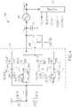
  • FIG. 4 is a diagram illustrating the relaxation oscillator 200 operating under an RC charging phase according to an embodiment of the present invention.
  • FIG. 5 is a diagram illustrating an RC charging operation according to an embodiment of the present invention.
  • the integration capacitor C INT is disconnected from the capacitors C1 and C2. Hence, the control input V INT at one plate of the integration capacitor C INT is not affected by the RC charging operation and remains unchanged.
  • the VCO 206 generates the output clock CKOUT in response to the control input V INT held by the integration capacitor C INT .
  • the phase generator 208 generates the switch control signal CK_P1 according to the output clock CKOUT, where the length T of the ON period of the switch control signal CK_P1 depends on the frequency of the output clock CKOUT. Specifically, the length T of the ON period of the switch control signal CK_P1 is inversely proportional to the frequency of the output clock CKOUT.
  • the voltage V CN at one plate of the capacitor C1 may be expressed by the following formula.
  • V DD represents a target voltage level indicative of zero frequency deviation
  • V OS 1 represents an offset resulting from frequency deviation
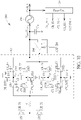
  • FIG. 6 is a diagram illustrating the relaxation oscillator 200 operating under an RC discharging phase according to an embodiment of the present invention.
  • FIG. 7 is a diagram illustrating an RC discharging operation according to an embodiment of the present invention.
  • the integration capacitor C INT is disconnected from the capacitors C1 and C2. Hence, the control input V INT at one plate of the integration capacitor C INT is not affected by the RC discharging operation and remains unchanged.
  • the VCO 206 generates the output clock CKOUT in response to the control input V INT held by the integration capacitor C INT .
  • the phase generator 208 generates the switch control signal CK_P2 according to the output clock CKOUT, where the length T of the ON period of the switch control signal CK_P2 is equal to the length T of the ON period of the switch control signal CK_P1, and also depends on the frequency of the output clock CKOUT.
  • the voltage V CP at one plate of the capacitor C2 may be expressed by the following formula.
  • V DD represents a target voltage level indicative of zero frequency deviation
  • V OS 2 represents an offset resulting from frequency deviation
  • the relaxation oscillator 200 enters the charge delivery phase. If the current frequency of the output clock CKOUT is equal to the target frequency value, both of the voltage V CN obtained at the end of the RC charging operation and the voltage V CP obtained at the end of the RC discharging operation should be equal to the same voltage level (e.g., 1 2 V DD ) . If the voltage V CN obtained at the end of the RC charging operation is different from the voltage V CP obtained at the end of the RC discharging operation, it means that the current frequency of the output clock CKOUT is deviated from the target frequency value, and the control input V INT should be adjusted to compensate for the frequency deviation.
  • the control input V INT should be adjusted to compensate for the frequency deviation.
  • the relaxation oscillator 200 enters the charge delivery phase for transferring the voltage difference ⁇ V to the integration capacitor C INT .
  • the voltage difference ⁇ V may be positive or negative, depending upon the length T of the ON period of the switch control signal CK_P1/CK_P2 (i.e., the frequency deviation direction of the output clock CKOUT).
  • FIG. 8 is a diagram illustrating the relaxation oscillator 200 operating under a charge delivery phase according to an embodiment of the present invention.
  • one plate of the capacitor C1 and another plate of the capacitor C2 are both connected to the inverting input terminal (-) of the unity-gain amplifier 204, and one plate of the capacitor C2 and another plate of the capacitor C1 are both connected to the output terminal of the unity-gain amplifier 204, where the output terminal of the unity-gain amplifier 204 is coupled to a non-inverting terminal (+) of the unity-gain amplifier 204.
  • the unity-gain amplifier 204 Since two plates of the capacitor C1 are coupled to the output terminal and the inverting input terminal of the unity-gain amplifier 204, respectively, the unity-gain amplifier 204 is operative to make two plates of the capacitor C1 have the same voltage level, meaning that charges stored in the capacitor C1 will be removed. Similarly, since two plates of the capacitor C2 are coupled to the output terminal and the inverting input terminal of the unity-gain amplifier 204, the unity-gain amplifier 204 is operative to make two plates of the capacitor C2 have the same voltage level, meaning that charges stored in the capacitor C2 will be removed.
  • FIG. 9 is a diagram illustrating a charge delivery operation according to an embodiment of the present invention.
  • the capacitors C1 and C2 may be configured to have the same capacitance value C.
  • the unity-gain amplifier 204 outputs the control input V INT held at the integration capacitor C INT at its output terminal.
  • the top plate voltage of the capacitor C1 becomes V INT + 1 2 V DD ⁇ V OS 1
  • the top plate voltage of the capacitor C2 becomes V INT + 1 2 V DD ⁇ V OS 2 .
  • charge re-distribution occurs among capacitors C1, C2, C INT , such that 1 2 V DD ⁇ C is transferred from the capacitor C1 to the capacitor C2, C ⁇ V OS 1 is transferred from the integration capacitor C INT to the capacitor C1, and C ⁇ V OS 2 is transferred from the integration capacitor C INT to the capacitor C2.
  • the unity-gain amplifier 204 sets the bottom plate voltage V BOT for both capacitors C1 and C2 by the same control input V INT,2 . Since the control input V INT held at the integration capacitor C INT is adjusted by the charge delivery operation performed by the unit-gain amplifier 204, the VCO 206 adjusts the frequency of the output clock CKOUT in response to the updated control input V INT,2 .
  • the VCO 206 may decrease the frequency of the output clock CKOUT.
  • the VCO 206 may increase the frequency of the output clock CKOUT.
  • FIG. 10 is a diagram illustrating the relaxation oscillator 200 operating under a reset phase according to an embodiment of the present invention.
  • one plate of the capacitor C1 is connected to the reference voltage GND
  • another plate of the capacitor C1 is connected to the reference voltage GND
  • one plate of the capacitor C2 is connected to the reference voltage V DD
  • another plate of the capacitor C2 is connected to the reference voltage GND.
  • the voltage V CN is discharged to the reference voltage GND
  • the voltage V CP is charged to the reference voltage V DD .
  • the voltage V CN is equal to the reference voltage GND
  • the voltage V CP is equal to the reference voltage V DD .
  • the relaxation oscillator 200 enters four phases (which include an RC charging phase, an RC discharging phase, a charge delivery phase, and a reset phase) again to reduce/cancel any frequency deviation still possessed by the output clock CKOUT.
  • FIG. 11 is a diagram illustrating a scenario where the frequency of the output clock CKOUT is deviated from the target frequency value.
  • FIG. 12 is a diagram illustrating a scenario where the frequency of the output clock CKOUT is equal to the target frequency value.
  • the ON period of the switch control signal CK_P1/CK_P2 is equal to T1 that is shorter than T2.
  • ⁇ V V CN -V CP > 0.
  • the positive voltage difference ⁇ V is subtracted from the current control input V INT , resulting in an updated control input V INT,2 with a lower voltage level.
  • the VCO 206 In response to the updated control input V INT,2 , the VCO 206 generates the output clock CKOUT with a lower frequency, which increases the ON period of the switch control signal CK_P1/CK_P2.
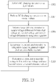
  • FIG. 13 is a flowchart illustrating a relaxation oscillation method according to an embodiment of the present invention.
  • the relaxation oscillation method may be employed by the relaxation oscillator 100/200. Provided that the result is substantially the same, the steps are not required to be executed in the exact order shown in FIG. 13 .
  • a resistor-capacitor (RC) charging operation is performed to set a first voltage.
  • an RC discharging operation is performed to set a second voltage.
  • a charge delivery operation is performed to sample a voltage difference between the first voltage and the second voltage and transfer the voltage difference to an integration capacitor.
  • an output clock is generated at a controllable oscillator in response to a control input provided by the integration capacitor.
  • a reset operation is performed to reset the first voltage to a first reference voltage and reset the second voltage to a second reference voltage.
  • the RC charging operation (RC charging phase) is followed by the RC discharging operation (RC discharging phase).
  • RC discharging phase may be followed by the RC charging operation (RC charging phase).
  • This alternative design also falls within the scope of the present invention.
  • the present invention may also be defined by the following numbered clauses .

Landscapes

  • Engineering & Computer Science (AREA)
  • Theoretical Computer Science (AREA)
  • Physics & Mathematics (AREA)
  • General Engineering & Computer Science (AREA)
  • General Physics & Mathematics (AREA)
  • Stabilization Of Oscillater, Synchronisation, Frequency Synthesizers (AREA)
  • Ceramic Capacitors (AREA)
  • Oscillators With Electromechanical Resonators (AREA)
  • Inductance-Capacitance Distribution Constants And Capacitance-Resistance Oscillators (AREA)

Abstract

A relaxation oscillator includes a resistor-capacitor (RC) circuit, an integration capacitor, a sampling circuit, and a controllable oscillator. The RC circuit performs an RC charging operation to set a first voltage, performs an RC discharging operation to set a second voltage, and performs a reset operation to reset the first voltage to a first reference voltage and reset the second voltage to a second reference voltage. The sampling circuit performs a charge delivery operation to sample a voltage difference between the first voltage and the second voltage, and transfers the voltage difference to the integration capacitor. The controllable oscillator generates an output clock in response to a control input provided by the integration capacitor.

Description

  • This application claims the benefit of U.S. provisional application No. 63/185,405 , filed on 05/07/2021 and incorporated herein by reference.
  • Background
  • The present invention relates to an oscillator design, and more particularly, to a relaxation oscillator that samples a voltage difference between voltages generated by resistor-capacitor (RC) charging and discharging for controlling an output clock frequency of a controllable oscillator and an associated relaxation oscillation method.
  • Many electronic devices operate using one or more clocks. These clocks are often generated using an oscillator. Many different oscillator types exist and can be implemented in different systems. Typical integrated circuits (ICs) often include one or more on-chip oscillators to develop clock signals . For example, a relaxation oscillator may be used to generate an output clock with a target frequency. One feature of the relaxation oscillator is that the relaxation oscillator is capable of generating the output clock without the need of a reference clock. A typical relaxation oscillator design may include a plurality of current sources and/or a continuous comparator. However, the continuous comparator is a power-hungry component, and the current source generally has high quiescent current. As a result, the typical relaxation oscillator design may fail to meet requirements of low-power applications. Thus, there is a need for an innovative ultra-low power relaxation oscillator design.
  • Summary
  • One of the objectives of the claimed invention is to provide a relaxation oscillator that samples a voltage difference between voltages generated by resistor-capacitor (RC) charging and discharging for controlling an output clock frequency of a controllable oscillator and an associated relaxation oscillation method.
  • According to a first aspect of the present invention, an exemplary relaxation oscillator is disclosed. The exemplary relaxation oscillator includes a resistor-capacitor (RC) circuit, an integration capacitor, a sampling circuit, and a controllable oscillator. The RC circuit is arranged to perform an RC charging operation to set a first voltage, perform an RC discharging operation to set a second voltage, and perform a reset operation to reset the first voltage to a first reference voltage and reset the second voltage to a second reference voltage. The sampling circuit is arranged to perform a charge delivery operation to sample a voltage difference between the first voltage and the second voltage and transfer the voltage difference to the integration capacitor. The controllable oscillator is arranged to generate an output clock in response to a control input provided by the integration capacitor.
  • According to a second aspect of the present invention, an exemplary relaxation oscillation method is disclosed. The exemplary relaxation oscillation method includes: performing a resistor-capacitor (RC) charging operation to set a first voltage; performing an RC discharging operation to set a second voltage; performing a charge delivery operation to sample a voltage difference between the first voltage and the second voltage and transfer the voltage difference to an integration capacitor; in response to a control input provided by the integration capacitor, generating an output clock at a controllable oscillator; and performing a reset operation to reset the first voltage to a first reference voltage and reset the second voltage to a second reference voltage.
  • These and other objectives of the present invention will no doubt become obvious to those of ordinary skill in the art after reading the following detailed description of the preferred embodiment that is illustrated in the various figures and drawings.
  • Brief Description of the Drawings
    • FIG. 1 is a block diagram illustrating fundamental architecture of a relaxation oscillator according to an embodiment of the present invention.
    • FIG. 2 is a diagram illustrating a circuit design of a relaxation oscillator according to an embodiment of the present invention.
    • FIG. 3 is a waveform diagram illustrating an output clock, a plurality of switch control signals, and an amplifier reset control signal according to an embodiment of the present invention.
    • FIG. 4 is a diagram illustrating a relaxation oscillator operating under an RC charging phase according to an embodiment of the present invention.
    • FIG. 5 is a diagram illustrating an RC charging operation according to an embodiment of the present invention.
    • FIG. 6 is a diagram illustrating a relaxation oscillator operating under an RC discharging phase according to an embodiment of the present invention.
    • FIG. 7 is a diagram illustrating an RC discharging operation according to an embodiment of the present invention.
    • FIG. 8 is a diagram illustrating a relaxation oscillator operating under a charge delivery phase according to an embodiment of the present invention.
    • FIG. 9 is a diagram illustrating a charge delivery operation according to an embodiment of the present invention.
    • FIG. 10 is a diagram illustrating a relaxation oscillator operating under a reset phase according to an embodiment of the present invention.
    • FIG. 11 is a diagram illustrating a scenario where a frequency of an output clock generated by a relaxation oscillator is deviated from a target frequency value.
    • FIG. 12 is a diagram illustrating a scenario where the frequency of the output clock by the relaxation oscillator is equal to the target frequency value.
    • FIG. 13 is a flowchart illustrating a relaxation oscillation method according to an embodiment of the present invention.
    Detailed Description
  • Certain terms are used throughout the following description and claims, which refer to particular components. As one skilled in the art will appreciate, electronic equipment manufacturers may refer to a component by different names. This document does not intend to distinguish between components that differ in name but not in function. In the following description and in the claims, the terms "include" and "comprise" are used in an open-ended fashion, and thus should be interpreted to mean "include, but not limited to ...". Also, the term "couple" is intended to mean either an indirect or direct electrical connection. Accordingly, if one device is coupled to another device, that connection may be through a direct electrical connection, or through an indirect electrical connection via other devices and connections.
  • FIG. 1 is a block diagram illustrating fundamental architecture of a relaxation oscillator according to an embodiment of the present invention. The relaxation oscillator 100 includes a resistor-capacitor (RC) circuit 102, a sampling circuit 104, an integration capacitor 106, a controllable oscillator 108, and a control signal generator circuit 110. The RC circuit 102 includes resistor (s) and capacitor(s), and is arranged to perform an RC charging operation to set one voltage VCN, perform an RC discharging operation to set another voltage VCP, and perform a reset operation to reset the voltage VCN to one reference voltage such as a ground voltage GND and reset the voltage VCP to another reference voltage such as a supply voltage VDD. For example, the RC circuit 102 may be implemented by a switched RC circuit. The sampling circuit 104 is arranged to perform a charge delivery operation to sample a voltage difference ΔV between two voltages VCN and VCP and transfer the voltage difference ΔV to the integration capacitor 106. For example, the sampling circuit 104 may be implemented by a unity-gain amplifier for amplifying the direct-current (DC) voltage. The controllable oscillator 108 is arranged to generate an output clock CKOUT in response to a control input (e.g., voltage input VINT) provided by the integration capacitor 106. For example, the controllable oscillator 108 may be implemented by a voltage-controlled oscillator (VCO), and a frequency of the output clock CKOUT is controlled by the voltage input of the VCO. The control signal generator circuit 110 is arranged to generate control signals for controlling operation timing of circuit components included in the RC circuit 102 and the sampling circuit 104. For example, the control signal generator circuit 110 may refer to the output clock CKOUT for generating a plurality of clock signals as the control signals, where a frequency of each control signal is lower than a frequency of the output clock CKOUT.
  • In this embodiment, the output clock CKOUT is generated from the controllable oscillator 108 with the control input VINT provided by the integration capacitor 106. Hence, no power-hungry continuous comparator is needed by the proposed relaxation oscillator 100. In addition, the RC circuit 102 is used to provide two voltages VCN and VCP from which the voltage difference ΔV is sampled for controlling the control input VINT at the integration capacitor 106. Hence, no current source with high quiescent current is needed by the proposed relaxation oscillator 100. In a case where the RC circuit 102 is implemented by a switched RC circuit, the switched RC circuit may operate under an RC switching frequency much lower the frequency of the output clock CKOUT. Hence, the power requirement of the switched RC circuit can be relaxed. In addition, the bandwidth requirement and power requirement of the following sampling circuit 104 can be relaxed. The control signals generated from the control signal generator circuit 110 may be non-overlapping clock signals used for non-overlapping phase control of the proposed relaxation oscillator 100. Hence, the control signal generator circuit 110 can be implemented by a simple logic circuit for power saving. Furthermore, circuit components of the RC circuit 102 and the sampling circuit 104 are active during ON periods (logic high periods) of related control signals generated from the control signal generator circuit 110 and are inactive during OFF periods (logic low periods) of related control signals generated from the control signal generator circuit 110. In other words, all circuit components of the RC circuit 102 and the sampling circuit 104 are not always in operation, which results in lower power consumption. To put it simply, the relaxation oscillator 100 employs an ultra-low power relaxation oscillator design. Further details of the relaxation oscillator 100 are described with reference to the accompanying drawings.
  • FIG. 2 is a diagram illustrating a circuit design of a relaxation oscillator according to an embodiment of the present invention. The relaxation oscillator 200 is based on the fundamental architecture of the relaxation oscillator 100 shown in FIG. 1. For example, the RC circuit 102 shown in FIG. 1 may be implemented by a switched RC circuit 202 shown in FIG. 2, the sampling circuit 104 shown in FIG. 1 may be implemented by a unity-gain amplifier 204 shown in FIG. 2, the integration capacitor 106 shown in FIG. 1 may be implemented by an integration capacitor CINT shown in FIG. 2, the controllable oscillator 108 shown in FIG. 1 may be implemented by a VCO 206 shown in FIG. 2, and the control signal generator circuit 110 shown in FIG. 1 may be implemented by a phase generator circuit (labeled as "Phase Gen.") 208 shown in FIG. 2.
  • It should be noted that, using the unity-gain amplifier 204 to realize the sampling circuit 104 is for illustrative purposes only, and is not meant to be a limitation of the present invention. In practice, any means capable of sampling a voltage difference between voltages generated by RC charging and RC discharging and transferring the sampled voltage difference to the following integration capacitor may be employed to implement the sampling circuit 104. These alternative designs all fall within the scope of the present invention.
  • The switched RC circuit 202 includes a resistor R, a plurality of capacitors C1, C2, and a plurality of switches SW1, SW2, SW3, SW4, SW5, SW6, SW7, SW8, SW9, SW10, SW11, SW12, SW13, and SW14. In this embodiment, the switched RC circuit 202 employs dual-phase RC charging/discharging for area saving. For example, the resistor R is used in an RC charging phase and reused in an RC discharging phase. However, this is for illustrative purposes only, and is not meant to be a limitation of the present invention. Alternatively, the switched RC circuit 202 may be modified to have one resistor and one capacitor used in an RC charging phase and another resistor and another capacitor used in an RC discharging phase.
  • The switches SW1-SW14 may be categorized into several switch-based circuits . A switch-based circuit, having switches SW1, SW4, SW6, is controlled by a same switch control signal CK_P1. A switch-based circuit, having switches SW2, SW10, SW12, is controlled by a same switch control signal CK_P2. A switch-based circuit, having switches SW5, SW7, SW11, SW13, is controlled by a same switch control signal CK_P3. A switch-based circuit, having switches SW3, SW8, SW9, SW14, is controlled by a same switch control signal CK_RST. In addition, the unity-gain amplifier 204 is controlled by an amplifier enable control signal AMP EN.
  • The switched RC circuit 202 is controlled by the switch control signals CK_P1, CK_P2, CK_P3, CK_RST and the unity-gain amplifier 204 is controlled by the amplifier enable control signal AMP_EN to enable the relaxation oscillator 200 to sequentially enter an RC charging phase, an RC discharging phase, a charge delivery phase, and a reset phase. An RC charging operation is performed at the switched RC circuit 202 during a first period (RC charging phase) . An RC discharging operation is performed at the switched RC circuit 202 during a second period (RC discharging phase). A charge delivery operation is performed by the unity-gain amplifier 204 during a third period (charge delivery phase). A reset operation is performed at the switched RC circuit 202 during a fourth period (reset phase) . The first period, and the second period, the third period, and the fourth period may be non-overlapping periods in the time domain. FIG. 3 is a waveform diagram illustrating the output clock CKOUT, the switch control signals CK_P1, CK_P2, CK_P3, CK_RST, and the amplifier reset control signal AMP_EN according to an embodiment of the present invention. The phase generator circuit 208 receives the output clock CKOUT, and generates the switch control signals CK_P1, CK_P2, CK_P3, CK_RST and the amplifier reset control signal AMP_EN according to the output clock CKOUT. The frequency of each of the switch control signals CK_P1, CK_P2, CK_P3, CK_RST and the amplifier reset control signal AMP_EN is lower than the frequency of the output clock CKOUT. For example, the frequency of the output clock CKOUT is 32K, and each of the switch control signals CK_P1, CK_P2, CK_P3, CK_RST and the amplifier reset control signal AMP EN is a clock signal with a frequency lower than 32K.
  • At the switched RC circuit 202, the RC charging operation is performed when the switch control signal CK_P1 has a logic high level, and is not performed when the switch control signal CK_P1 has a logic low level. Specifically, the switches SW1, SW4, SW6 are switched on during an ON period of the switch control signal CK_P1 (CK_P1=1), and are switched off during an OFF period of the switch control signal CK_P1 (CK_P1=0). The RC charging operation is performed once per N clock cycles of the output clock CKOUT, where N is an integer larger than one. As shown in FIG. 3, the RC charging operation may be performed once per 16 clock cycles of the output clock CKOUT.
  • At the switched RC circuit 202, the RC discharging operation is performed when the switch control signal CK_P2 has a logic high level, and is not performed when the switch control signal CK_P2 has a logic low level. Specifically, the switches SW2, SW10, SW12 are switched on during an ON period of the switch control signal CK_P2 (CK_P2=1), and are switched off during an OFF period of the switch control signal CK_P2 (CK_P2=0). The RC discharging operation is performed once per N clock cycles of the output clock CKOUT, where N is an integer larger than one. As shown in FIG. 3, the RC discharging operation may be performed once per 16 clock cycles of the output clock CKOUT.
  • At the unity-gain amplifier 204, the charge delivery operation is performed when the switch control signal CK_P3 has a logic high level, and is not performed when the switch control signal CK_P3 has a logic low level. Specifically, the switches SW5, SW7, SW11, SW13 are switched on during an ON period of the switch control signal CK_P3 (CK_P3=1), and are switched off during an OFF period of the switch control signal CK_P3 (CK_P3=0). The charge delivery operation is performed once per N clock cycles of the output clock CKOUT, where N is an integer larger than one. As shown in FIG. 3, the charge delivery operation may be performed once per 16 clock cycles of the output clock CKOUT.
  • At the switched RC circuit 202, the reset operation is performed when the switch control signal CK_RST has a logic high level, and is not performed when the switch control signal CK RST has a logic low level. Specifically, the switches SW3, SW8, SW9, SW14 are switched on during an ON period of the switch control signal CK_RST (CK_RST=1), and are switched off during an OFF period of the switch control signal CK RST (CK_RST=0) . The reset operation is performed once per N clock cycles of the output clock CKOUT, where N is an integer larger than one. As shown in FIG. 3, the reset operation may be performed once per 16 clock cycles of the output clock CKOUT.
  • Regarding the unity-gain amplifier 204, it is responsible for dealing with the charge delivery operation that transfers the voltage difference ΔV (ΔV=VCN-VCP) from the preceding switched RC circuit 202 to the following integration capacitor CINT. An ON period of the amplifier enable control signal AMP_EN overlaps an ON period of the switch control signal CK_P3, and is not shorter than the ON period of the switch control signal CK_P3. To ensure a stable operation of the unity-gain amplifier 204 during the charge delivery operation, a start time of the ON period of the amplifier enable control signal AMP_EN may be intentionally advanced to be earlier than a start time of the ON period of the switch control signal CK_P3, and an end time of the ON period of the amplifier enable control signal AMP EN may be internally delayed to be later than an end time of the ON period of the switch control signal CK_P3. In this embodiment, one ON period of the amplifier enable control signal AMP_EN lasts for 11 clock cycles of the output clock CKOUT, which is approximately 70% of 16 clock cycles of the output clock CKOUT. In other words, the unity-gain amplifier 204 may be controlled by the amplifier enable control signal AMP_EN with 70% duty cycle for power saving. However, this is for illustrative purposes only, and is not meant to be a limitation of the present invention. Furthermore, the ON period of the amplifier enable control signal AMP_EN does not overlap any of the ON period of the switch control signal CK_P1, the ON period of the switch control signal CK P2, and the ON period of the switch control signal CK_RST.
  • The relaxation oscillator 200 may enter four phases (which include an RC charging phase, an RC discharging phase, a charge delivery phase, and a reset phase) sequentially and repeatedly, for reducing the frequency deviation of the output clock CKOUT and making the frequency of the output clock CKOUT have the target frequency value. FIG. 4 is a diagram illustrating the relaxation oscillator 200 operating under an RC charging phase according to an embodiment of the present invention. The switches SW1, SW4, SW6 are switched on by the switch control signal CK_P1 (CK_P1=1). The switches SW2, SW10, SW12 are switched off by the switch control signal CK P2 (CK_P2=0), such that one end of the resistor R is disconnected from the reference voltage GND, one plate of the capacitor C2 is disconnected from another end of the resistor R, and another plate of the capacitor C2 is disconnected from the reference voltage GND. The switches SW5, SW7, SW11, SW13 are switched off by the switch control signal CK_P3 (CK_P3=0), such that two plates of the capacitor C1 and two plates of the capacitor C2 are all disconnected from the unity-gain amplifier 204. The switches SW3, SW8, SW9, SW14 are switched off by the switch control signal CK_RST (CK_RTS=0), such that one plate of the capacitor C1 is disconnected from the reference voltage GND, another plate of the capacitor C1 is disconnected from the reference voltage GND, one plate of the capacitor C2 is disconnected from the reference voltage VDD, and another plate of the capacitor C2 is disconnected from the reference voltage GND. In addition, the unity-gain amplifier 204 is disabled by the amplifier enable control signal AMP_EN (AMP_EN=0) .
  • During the period in which the RC charging operation is performed, one end of the resistor R is connected to the reference voltage VDD, one plate of the capacitor C1 is connected to another end of the resistor R, and another plate of the capacitor C1 is connected to the reference voltage GND. Hence, the voltage VCN at one plate of the capacitor C1 is charged from an initial voltage level (e.g., reference voltage GND) through RC charging. FIG. 5 is a diagram illustrating an RC charging operation according to an embodiment of the present invention. The integration capacitor CINT is disconnected from the capacitors C1 and C2. Hence, the control input VINT at one plate of the integration capacitor CINT is not affected by the RC charging operation and remains unchanged. The VCO 206 generates the output clock CKOUT in response to the control input VINT held by the integration capacitor CINT. The phase generator 208 generates the switch control signal CK_P1 according to the output clock CKOUT, where the length T of the ON period of the switch control signal CK_P1 depends on the frequency of the output clock CKOUT. Specifically, the length T of the ON period of the switch control signal CK_P1 is inversely proportional to the frequency of the output clock CKOUT. At the end of the RC charging operation, the voltage VCN at one plate of the capacitor C1 may be expressed by the following formula. V CN = V DD 1 e T RC 1 = 1 2 V DD V OS 1
    Figure imgb0001
  • In above formula (1), 1 2 V DD
    Figure imgb0002
    represents a target voltage level indicative of zero frequency deviation, and V OS1 represents an offset resulting from frequency deviation.
  • FIG. 6 is a diagram illustrating the relaxation oscillator 200 operating under an RC discharging phase according to an embodiment of the present invention. The switches SW2, SW10, SW12 are switched on by the switch control signal CK_P2 (CK_P2=1). The switches SW1, SW4, SW6 are switched off by the switch control signal CK_P1 (CK_P1=0), such that one end of the resistor R is disconnected from the reference voltage VDD, one plate of the capacitor C1 is disconnected from another end of the resistor R, and another plate of the capacitor C1 is disconnected from the reference voltage GND. The switches SW5, SW7, SW11, SW13 are switched off by the switch control signal CK_P3 (CK_P3=0), such that two plates of the capacitor C1 and two plates of the capacitor C2 are all disconnected from the unity-gain amplifier 204. The switches SW3, SW8, SW9, SW14 are switched off by the switch control signal CK_RST (CK_RTS=0), such that one plate of the capacitor C1 is disconnected from the reference voltage GND, another plate of the capacitor C1 is disconnected from the reference voltage GND, one plate of the capacitor C2 is disconnected from the reference voltage VDD, and another plate of the capacitor C2 is disconnected from the reference voltage GND. In addition, the unity-gain amplifier 204 is disabled by the amplifier enable control signal AMP_EN (AMP_EN=0).
  • During the period in which the RC discharging operation is performed, one end of the resistor R is connected to the reference voltage GND, one plate of the capacitor C2 is connected to another end of the resistor R, and another plate of the capacitor C2 is connected to the reference voltage GND. Hence, the voltage VCP at one plate of the capacitor C2 is discharged from an initial voltage level (e.g., reference voltage VDD) through RC discharging. FIG. 7 is a diagram illustrating an RC discharging operation according to an embodiment of the present invention. The integration capacitor CINT is disconnected from the capacitors C1 and C2. Hence, the control input VINT at one plate of the integration capacitor CINT is not affected by the RC discharging operation and remains unchanged. The VCO 206 generates the output clock CKOUT in response to the control input VINT held by the integration capacitor CINT. The phase generator 208 generates the switch control signal CK_P2 according to the output clock CKOUT, where the length T of the ON period of the switch control signal CK_P2 is equal to the length T of the ON period of the switch control signal CK_P1, and also depends on the frequency of the output clock CKOUT. At the end of the RC discharging operation, the voltage VCP at one plate of the capacitor C2 may be expressed by the following formula. V CP = V DD e T RC 2 = 1 2 V DD + V OS 2
    Figure imgb0003
  • In above formula (2), 1 2 V DD
    Figure imgb0004
    represents a target voltage level indicative of zero frequency deviation, and V OS2 represents an offset resulting from frequency deviation.
  • After the RC charging phase and the RC discharging phase are completed, the relaxation oscillator 200 enters the charge delivery phase. If the current frequency of the output clock CKOUT is equal to the target frequency value, both of the voltage VCN obtained at the end of the RC charging operation and the voltage VCP obtained at the end of the RC discharging operation should be equal to the same voltage level (e.g., 1 2 V DD )
    Figure imgb0005
    . If the voltage VCN obtained at the end of the RC charging operation is different from the voltage VCP obtained at the end of the RC discharging operation, it means that the current frequency of the output clock CKOUT is deviated from the target frequency value, and the control input VINT should be adjusted to compensate for the frequency deviation. In this embodiment, there is a voltage difference ΔV (ΔV=VCN-VCP=VOS1+VOS2) between the voltage VCN obtained at the end of the RC charging operation and the voltage VCP obtained at the end of the RC discharging operation, as illustrated in FIG. 5 and FIG. 7. The relaxation oscillator 200 enters the charge delivery phase for transferring the voltage difference ΔV to the integration capacitor CINT. It should be noted that the voltage difference ΔV may be positive or negative, depending upon the length T of the ON period of the switch control signal CK_P1/CK_P2 (i.e., the frequency deviation direction of the output clock CKOUT).
  • FIG. 8 is a diagram illustrating the relaxation oscillator 200 operating under a charge delivery phase according to an embodiment of the present invention. The switches SW5, SW7, SW11, SW13 are switched on by the switch control signal CK_P3 (CK_P3=1). The switches SW1, SW4, SW6 are switched off by the switch control signal CK_P1 (CK_P1=0), such that one end of the resistor R is disconnected from the reference voltage VDD, one plate of the capacitor C1 is disconnected from another end of the resistor R, and another plate of the capacitor C1 is disconnected from the reference voltage GND. The switches SW2, SW10, SW12 are switched off by the switch control signal CK_P2 (CK_P2=0), such that one end of the resistor R is disconnected from the reference voltage GND, one plate of the capacitor C2 is disconnected from another end of the resistor R, and another plate of the capacitor C2 is disconnected from the reference voltage GND. The switches SW3, SW8, SW9, SW14 are switched off by the switch control signal CK_RST (CK_RST=0), such that one plate of the capacitor C1 is disconnected from the reference voltage GND, another plate of the capacitor C1 is disconnected from the reference voltage GND, one plate of the capacitor C2 is disconnected from the reference voltage VDD, and another plate of the capacitor C2 is disconnected from the reference voltage GND. In addition, the unity-gain amplifier 204 is enabled by the amplifier enable control signal AMP_EN (AMP_EN=1).
  • During the period in which the charge delivery operation is performed by the unity-gain amplifier 204, one plate of the capacitor C1 and another plate of the capacitor C2 are both connected to the inverting input terminal (-) of the unity-gain amplifier 204, and one plate of the capacitor C2 and another plate of the capacitor C1 are both connected to the output terminal of the unity-gain amplifier 204, where the output terminal of the unity-gain amplifier 204 is coupled to a non-inverting terminal (+) of the unity-gain amplifier 204. Since two plates of the capacitor C1 are coupled to the output terminal and the inverting input terminal of the unity-gain amplifier 204, respectively, the unity-gain amplifier 204 is operative to make two plates of the capacitor C1 have the same voltage level, meaning that charges stored in the capacitor C1 will be removed. Similarly, since two plates of the capacitor C2 are coupled to the output terminal and the inverting input terminal of the unity-gain amplifier 204, the unity-gain amplifier 204 is operative to make two plates of the capacitor C2 have the same voltage level, meaning that charges stored in the capacitor C2 will be removed. In this embodiment, a charge difference ΔQ (ΔQ=ΔV/CINT) resulting from the voltage difference ΔV (ΔV=VCN-VCP=VOS1+VOS2) is applied to the integration capacitor CINT due to charge re-distribution among capacitors C1, C2, CINT.
  • FIG. 9 is a diagram illustrating a charge delivery operation according to an embodiment of the present invention. The capacitors C1 and C2 may be configured to have the same capacitance value C. At the time the switches SW5, SW7, SW11, SW13 are switched on, the unity-gain amplifier 204 outputs the control input VINT held at the integration capacitor CINT at its output terminal. Hence, as illustrated in the top half of FIG. 9, the bottom plate voltage VBOT for both capacitors C1 and C2 is set by the same control input VINT (VBOT=VINT). At this moment, the top plate voltage of the capacitor C1 becomes V INT + 1 2 V DD V OS 1
    Figure imgb0006
    , and the top plate voltage of the capacitor C2 becomes V INT + 1 2 V DD V OS 2
    Figure imgb0007
    . Next, charge re-distribution occurs among capacitors C1, C2, CINT, such that 1 2 V DD C
    Figure imgb0008
    is transferred from the capacitor C1 to the capacitor C2, C · V OS1 is transferred from the integration capacitor CINT to the capacitor C1, and C · V OS2 is transferred from the integration capacitor CINT to the capacitor C2. After the charge re-distribution is done, the control input VINT held at the integration capacitor CINT is updated to VINT,2 (V INT,2 = VINT - C · (V OS1 + V OS2 )/CINT) as illustrated in the bottom half of FIG. 9. In addition, the unity-gain amplifier 204 sets the bottom plate voltage VBOT for both capacitors C1 and C2 by the same control input VINT,2. Since the control input VINT held at the integration capacitor CINT is adjusted by the charge delivery operation performed by the unit-gain amplifier 204, the VCO 206 adjusts the frequency of the output clock CKOUT in response to the updated control input VINT,2. For example, when the voltage difference ΔV (ΔV=VCN-VCP) is positive, the VCO 206 may decrease the frequency of the output clock CKOUT. For another example, when the voltage difference ΔV (ΔV=VCN-VCP) is negative, the VCO 206 may increase the frequency of the output clock CKOUT.
  • After the charge delivery phase is completed, the relaxation oscillator 200 enters the reset phase for resetting the voltage VCN to an initial voltage level (e.g., reference voltage GND) and resetting the voltage VCP to an initial voltage level (e.g., reference voltage VDD) for a next round of frequency deviation detection and calibration. FIG. 10 is a diagram illustrating the relaxation oscillator 200 operating under a reset phase according to an embodiment of the present invention. The switches SW3, SW8, SW9, SW14 are switched on by the switch control signal CK_RST (CK_RST=1). The switches SW1, SW4, SW6 are switched off by the switch control signal CK_P1 (CK_P1=0), such that one end of the resistor R is disconnected from the reference voltage VDD, one plate of the capacitor C1 is disconnected from another end of the resistor R, and another plate of the capacitor C1 is disconnected from the reference voltage GND. The switches SW2, SW10, SW12 are switched off by the switch control signal CK_P2 (CK_P2=0), such that one end of the resistor R is disconnected from the reference voltage GND, one plate of the capacitor C2 is disconnected from another end of the resistor R, and another plate of the capacitor C2 is disconnected from the reference voltage GND. The switches SW5, SW7, SW11, SW13 are switched off by the switch control signal CK_P3 (CK_P3=0), such that two plates of the capacitor C1 and two plates of the capacitor C2 are all disconnected from the unity-gain amplifier 204. In addition, the unity-gain amplifier 204 is disabled by the amplifier enable control signal AMP_EN (AMP_EN=0).
  • During the period in which the reset operation is performed by the switched RC circuit 202, one plate of the capacitor C1 is connected to the reference voltage GND, another plate of the capacitor C1 is connected to the reference voltage GND, one plate of the capacitor C2 is connected to the reference voltage VDD, and another plate of the capacitor C2 is connected to the reference voltage GND. Hence, during the period of the reset operation, the voltage VCN is discharged to the reference voltage GND, and the voltage VCP is charged to the reference voltage VDD. At the end of the reset operation, the voltage VCN is equal to the reference voltage GND, and the voltage VCP is equal to the reference voltage VDD. After the reset phase is completed, the relaxation oscillator 200 enters four phases (which include an RC charging phase, an RC discharging phase, a charge delivery phase, and a reset phase) again to reduce/cancel any frequency deviation still possessed by the output clock CKOUT.
  • The frequency deviation of the output clock CKOUT is reflected in the voltage difference ΔV (ΔV=VCN-VCP) between the voltage VCN obtained at the end of the RC charging operation and the voltage VCP obtained at the end of the RC discharging operation. Hence, to reduce the non-zero frequency deviation of the output clock CKOUT as indicated by the non-zero voltage difference ΔV, the control input VINT of the VCO 206 needs to be adjusted by the non-zero voltage difference ΔV. FIG. 11 is a diagram illustrating a scenario where the frequency of the output clock CKOUT is deviated from the target frequency value. FIG. 12 is a diagram illustrating a scenario where the frequency of the output clock CKOUT is equal to the target frequency value. Assuming that the current frequency of the output clock CKOUT is higher than the target frequency value, the ON period of the switch control signal CK_P1/CK_P2 is equal to T1 that is shorter than T2. Hence, there is a positive voltage difference ΔV between the voltage VCN obtained at the end of the RC charging operation and the voltage VCP obtained at the end of the RC discharging operation, that is, ΔV = VCN-VCP > 0. The positive voltage difference ΔV (ΔV=ΔQ/CINT) is transferred to the integration capacitor CINT. Hence, the positive voltage difference ΔV is subtracted from the current control input VINT, resulting in an updated control input VINT,2 with a lower voltage level. In response to the updated control input VINT,2, the VCO 206 generates the output clock CKOUT with a lower frequency, which increases the ON period of the switch control signal CK_P1/CK_P2. Suppose that the frequency of the output clock CKOUT is equal to the target frequency value under the control of the updated control input VINT,2 fed into the VCO 206. Since the ON period of the switch control signal CK_P1/CK_P2 is equal to T2, there is no voltage difference ΔV (ΔV=0) between the voltage VCN obtained at the end of the RC charging operation and the voltage VCP obtained at the end of the RC discharging operation, such that no voltage adjustment is made to the current control input VINT (VINT=VINT,2).
  • FIG. 13 is a flowchart illustrating a relaxation oscillation method according to an embodiment of the present invention. The relaxation oscillation method may be employed by the relaxation oscillator 100/200. Provided that the result is substantially the same, the steps are not required to be executed in the exact order shown in FIG. 13. At step 1302, a resistor-capacitor (RC) charging operation is performed to set a first voltage. At step 1304, an RC discharging operation is performed to set a second voltage. At step 1306, a charge delivery operation is performed to sample a voltage difference between the first voltage and the second voltage and transfer the voltage difference to an integration capacitor. At step 1308, an output clock is generated at a controllable oscillator in response to a control input provided by the integration capacitor. At step 1310, a reset operation is performed to reset the first voltage to a first reference voltage and reset the second voltage to a second reference voltage. As a person skilled in the art can readily understand details of each step after reading above paragraphs directed to the relaxation oscillator 100/200, further description is omitted here for brevity.
  • In above embodiments, the RC charging operation (RC charging phase) is followed by the RC discharging operation (RC discharging phase). However, this is for illustrative purposes only, and is not meant to be a limitation of the present invention. Alternatively, the RC discharging operation (RC discharging phase) may be followed by the RC charging operation (RC charging phase). The same objective of creating two voltages VCN and VCP to indicate a frequency status of the output clock CKOUT before the charge delivery operation (charge delivery) is achieved. This alternative design also falls within the scope of the present invention.
  • Those skilled in the art will readily observe that numerous modifications and alterations of the device and method may be made while retaining the teachings of the invention. Accordingly, the above disclosure should be construed as limited only by the metes and bounds of the appended claims.
  • The present invention may also be defined by the following numbered clauses .
    1. 1. A relaxation oscillator comprising:
      • a resistor-capacitor (RC) circuit, arranged to perform an RC charging operation to set a first voltage, perform an RC discharging operation to set a second voltage, and perform a reset operation to reset the first voltage to a first reference voltage and reset the second voltage to a second reference voltage; an integration capacitor;
      • a sampling circuit, arranged to perform a charge delivery operation to sample a voltage difference between the first voltage and the second voltage and transfer the voltage difference to the integration capacitor; and
      • a controllable oscillator, arranged to generate an output clock in response to a control input provided by the integration capacitor.
    2. 2. The relaxation oscillator of clause 1, wherein the RC charging operation is performed during a first period; the RC discharging operation is performed during a second period; the charge delivery operation is performed during a third period; the reset operation is performed during a fourth period; and the first period, the second period, the third period, and the fourth period are non-overlapping periods.
    3. 3. The relaxation oscillator of clause 1, wherein the RC circuit is a switched RC circuit comprising:
      • a resistor;
      • a first capacitor, have one plate at which the first voltage is held;
      • a second capacitor, having one plate at which the second voltage is held; and
      • a switch network;
      • wherein during a period in which the RC charging operation is performed, the switch network is configured to connect the resistor to the first capacitor and disconnect the resistor from the second capacitor; and during a period in which the RC discharging operation is performed, the switch network is configured to connect the resistor to the second capacitor and disconnect the resistor from the first capacitor.
    4. 4. The relaxation oscillator of clause 3, wherein the switch network comprises: a switch-based circuit, wherein during the period in which the RC charging operation is performed, the switch-based circuit is configured to connect one end of the resistor to the second reference voltage, connect said one plate of the first capacitor to another end of the resistor, and connect another plate of the first capacitor to the first reference voltage; and during a period in which the RC charging operation is not performed, the switch-based circuit is configured to disconnect said one end of the resistor from the second reference voltage, disconnect said one plate of the first capacitor from said another end of the resistor, and disconnect said another plate of the first capacitor from the first reference voltage.
    5. 5. The relaxation oscillator of clause 4, further comprising:
      a control signal generator circuit, arranged to generate a switch control signal according to the output clock, and provide the switch control signal to the switch-based circuit, wherein a frequency of the switch control signal is lower than a frequency of the output clock.
    6. 6. The relaxation oscillator of clause 3, wherein the switch network comprises: a switch-based circuit, wherein during the period in which the RC discharging operation is performed, the switch-based circuit is configured to connect one end of the resistor to the first reference voltage, connect said one plate of the second capacitor to another end of the resistor, and connect another plate of the second capacitor to the first reference voltage; and during a period in which the RC discharging operation is not performed, the switch-based circuit is configured to disconnect said one end of the resistor from the first reference voltage, disconnect said one plate of the second capacitor from said another end of the resistor, and disconnect said another plate of the second capacitor from the first reference voltage.
    7. 7. The relaxation oscillator of clause 6, further comprising:
      a control signal generator circuit, arranged to generate a switch control signal according to the output clock, and provide the switch control signal to the switch-based circuit, wherein a frequency of the switch control signal is lower than a frequency of the output clock.
    8. 8. The relaxation oscillator of clause 3, wherein the switch network comprises: a switch-based circuit, wherein during a period in which the charge delivery operation is performed, the switch-based circuit is configured to connect said one plate of the first capacitor, another plate of the first capacitor, said one plate of the second capacitor, and another plate of the second capacitor to the sampling circuit; and during a period in which the charge delivery operation is not performed, the switch-based circuit is configured to disconnect said one plate of the first capacitor, said another plate of the first capacitor, said one plate of the second capacitor, and said another plate of the second capacitor from the sampling circuit.
    9. 9. The relaxation oscillator of clause 8, further comprising:
      a control signal generator circuit, arranged to generate a switch control signal according to the output clock, and provide the switch control signal to the switch-based circuit, wherein a frequency of the switch control signal is lower than a frequency of the output clock.
    10. 10. The relaxation oscillator of clause 8, wherein the sampling circuit comprises:
      • a unity-gain amplifier, having a non-inverting input terminal, an inverting input terminal, and an output terminal, where the output terminal is coupled to the non-inverting input terminal, and the inverting input terminal is coupled to the integration capacitor;
      • during the period in which the charge delivery operation is performed, the switch-based circuit is configured to connect said one plate of the first capacitor and said another plate of the second capacitor to the inverting input terminal of the unity-gain amplifier, and is further configured to connect said another plate of the first capacitor and said one plate of the second capacitor to the output terminal of the unity-gain amplifier; and
      • during the period in which the charge delivery operation is not performed, the switch-based circuit is configured to disconnect said one plate of the first capacitor and said another plate of the second capacitor from the inverting input terminal of the unity-gain amplifier, and is further configured to disconnect said another plate of the first capacitor and said one plate of the second capacitor from the output terminal of the unity-gain amplifier.
    11. 11. The relaxation oscillator of clause 10, wherein the inverting input terminal of the unity-gain amplifier is coupled to one plate of the integration capacitor, another plate of the integration capacitor is coupled to the first reference voltage, and the control input of the controllable oscillator is held at said one plate of the integration capacitor.
    12. 12. The relaxation oscillator of clause 10, wherein the unity-gain amplifier is enabled during the period in which the charge delivery operation is performed, and is disabled during the period in which the RC charging operation is performed, the period in which the RC discharging operation is performed, and a period in which the reset operation is performed.
    13. 13. The relaxation oscillator of clause 10, further comprising:
      a control signal generator circuit, arranged to generate an amplifier enable control signal according to the output clock, and provide the amplifier enable control signal to the unity-gain amplifier, wherein a frequency of the amplifier enable control signal is lower than a frequency of the output clock.
    14. 14. The relaxation oscillator of clause 3, wherein the switch network comprises: a switch-based circuit, wherein during a period in which the reset operation is performed, the switch-based circuit is configured to connect said one plate of the first capacitor to the first reference voltage, connect another plate of the first capacitor to the first reference voltage, connect said one plate of the second capacitor to the second reference voltage, and connect another plate of the second capacitor to the first reference voltage; and during a period in which the reset operation is not performed, the switch-based circuit is configured to disconnect said one plate of the first capacitor from the first reference voltage, disconnect said another plate of the first capacitor from the first reference voltage, disconnect said one plate of the second capacitor from the second reference voltage, and disconnect said another plate of the second capacitor from the first reference voltage.
    15. 15. The relaxation oscillator of clause 14, further comprising:
      a control signal generator circuit, arranged to generate a switch control signal according to the output clock, and provide the switch control signal to the switch-based circuit, wherein a frequency of the switch control signal is lower than a frequency of the output clock.
    16. 16. A relaxation oscillation method comprising:
      • performing a resistor-capacitor (RC) charging operation to set a first voltage;
      • performing an RC discharging operation to set a second voltage;
      • performing a charge delivery operation to sample a voltage difference between the first voltage and the second voltage and transfer the voltage difference to an integration capacitor;
      • in response to a control input provided by the integration capacitor, generating an output clock at a controllable oscillator; and
      • performing a reset operation to reset the first voltage to a first reference voltage and reset the second voltage to a second reference voltage.
    17. 17. The relaxation oscillation method of clause 16, wherein the RC charging operation is performed once per N clock cycles of the output clock, where N is an integer larger than one.
    18. 18. The relaxation oscillation method of clause 16, wherein the RC discharging operation is performed once per N clock cycles of the output clock, where N is an integer larger than one.
    19. 19. The relaxation oscillation method of clause 16, wherein the charge delivery operation is performed once per N clock cycles of the output clock, where N is an integer larger than one.
    20. 20. The relaxation oscillation method of clause 16, wherein the reset operation is performed once per N clock cycles of the output clock, where N is an integer larger than one.

Claims (15)

  1. A relaxation oscillator (100, 200) comprising:
    a resistor-capacitor, RC, circuit (102, 202), arranged to perform an RC charging operation to set a first voltage, perform an RC discharging operation to set a second voltage, and perform a reset operation to reset the first voltage to a first reference voltage and reset the second voltage to a second reference voltage;
    an integration capacitor (106, CINT);
    a sampling circuit (104), arranged to perform a charge delivery operation to sample a voltage difference between the first voltage and the second voltage and transfer the voltage difference to the integration capacitor (106 CINT); and
    a controllable oscillator (108), arranged to generate an output clock in response to a control input provided by the integration capacitor (106, CINT).
  2. The relaxation oscillator (100, 200) of claim 1, wherein the RC charging operation is performed during a first period; the RC discharging operation is performed during a second period; the charge delivery operation is performed during a third period; the reset operation is performed during a fourth period; and the first period, the second period, the third period, and the fourth period are non-overlapping periods.
  3. The relaxation oscillator (100, 200) of claim 1, wherein the RC circuit (102, 202) is a switched RC circuit (102, 202) comprising:
    a resistor (R);
    a first capacitor(C1), have one plate at which the first voltage is held;
    a second capacitor (C2), having one plate at which the second voltage is held; and
    a switch network (SW1, SW2, SW3, SW4, SW5, SW6, SW7, SW8, SW9, SW10, SW11, SW12, SW13, SW14);
    wherein during a period in which the RC charging operation is performed, the switch network (SW1, SW2, SW3, SW4, SW5, SW6, SW7, SW8, SW9, SW10, SW11, SW12, SW13, SW14) is configured to connect the resistor (R) to the first capacitor (C1) and disconnect the resistor (R) from the second capacitor (C2) ; and during a period in which the RC discharging operation is performed, the switch network (SW1, SW2, SW3, SW4, SW5, SW6, SW7, SW8, SW9, SW10, SW11, SW12, SW13, SW14) is configured to connect the resistor (R)to the second capacitor (C2) and disconnect the resistor (R) from the first capacitor (C1).
  4. The relaxation oscillator (100, 200) of claim 3, wherein the switch network (SW1, SW2, SW3, SW4, SW5, SW6, SW7, SW8, SW9, SW10, SW11, SW12, SW13, SW14) comprises:
    a switch-based circuit, wherein during the period in which the RC charging operation is performed, the switch-based circuit is configured to connect one end of the resistor (R) to the second reference voltage, connect said one plate of the first capacitor (C1) to another end of the resistor (R), and connect another plate of the first capacitor (C1) to the first reference voltage; and during a period in which the RC charging operation is not performed, the switch-based circuit is configured to disconnect said one end of the resistor (R) from the second reference voltage, disconnect said one plate of the first capacitor (C1) from said another end of the resistor (R), and disconnect said another plate of the first capacitor (C1) from the first reference voltage.
  5. The relaxation oscillator (100, 200) of claim 4, further comprising:
    a control signal generator circuit (110), arranged to generate a switch control signal according to the output clock, and provide the switch control signal to the switch-based circuit, wherein a frequency of the switch control signal is lower than a frequency of the output clock.
  6. The relaxation oscillator (100, 200) of claim 3, wherein the switch network (SW1, SW2, SW3, SW4, SW5, SW6, SW7, SW8, SW9, SW10, SW11, SW12, SW13, SW14) comprises:
    a switch-based circuit, wherein during the period in which the RC discharging operation is performed, the switch-based circuit is configured to connect one end of the resistor (R)to the first reference voltage, connect said one plate of the second capacitor (C2) to another end of the resistor (R), and connect another plate of the second capacitor (C2) to the first reference voltage; and during a period in which the RC discharging operation is not performed, the switch-based circuit is configured to disconnect said one end of the resistor (R) from the first reference voltage, disconnect said one plate of the second capacitor (C2) from said another end of the resistor (R), and disconnect said another plate of the second capacitor (C2) from the first reference voltage.
  7. The relaxation oscillator (100, 200) of claim 6, further comprising:
    a control signal generator circuit (110), arranged to generate a switch control signal according to the output clock, and provide the switch control signal to the switch-based circuit, wherein a frequency of the switch control signal is lower than a frequency of the output clock.
  8. The relaxation oscillator (100, 200) of claim 3, wherein the switch network (SW1, SW2, SW3, SW4, SW5, SW6, SW7, SW8, SW9, SW10, SW11, SW12, SW13, SW14) comprises:
    a switch-based circuit, wherein during a period in which the charge delivery operation is performed, the switch-based circuit is configured to connect said one plate of the first capacitor (C1), another plate of the first capacitor (C1), said one plate of the second capacitor (C2), and another plate of the second capacitor (C2) to the sampling circuit (104) ; and during a period in which the charge delivery operation is not performed, the switch-based circuit is configured to disconnect said one plate of the first capacitor (C1), said another plate of the first capacitor (C1), said one plate of the second capacitor (C2), and said another plate of the second capacitor (C2) from the sampling circuit (104).
  9. The relaxation oscillator (100, 200) of claim 8, further comprising:
    a control signal generator circuit (110), arranged to generate a switch control signal according to the output clock, and provide the switch control signal to the switch-based circuit, wherein a frequency of the switch control signal is lower than a frequency of the output clock.
  10. The relaxation oscillator (100, 200) of claim 8, wherein the sampling circuit (104) comprises:
    a unity-gain amplifier (204), having a non-inverting input terminal, an inverting input terminal, and an output terminal, where the output terminal is coupled to the non-inverting input terminal, and the inverting input terminal is coupled to the integration capacitor (106, CINT);
    during the period in which the charge delivery operation is performed, the switch-based circuit is configured to connect said one plate of the first capacitor (C1) and said another plate of the second capacitor (C2) to the inverting input terminal of the unity-gain amplifier (204), and is further configured to connect said another plate of the first capacitor (C1) and said one plate of the second capacitor (C2) to the output terminal of the unity-gain amplifier (204); and
    during the period in which the charge delivery operation is not performed, the switch-based circuit is configured to disconnect said one plate of the first capacitor (C1) and said another plate of the second capacitor (C2) from the inverting input terminal of the unity-gain amplifier (204), and is further configured to disconnect said another plate of the first capacitor (C1) and said one plate of the second capacitor (C2) from the output terminal of the unity-gain amplifier (204) .
  11. The relaxation oscillator (100, 200) of claim 10, wherein the inverting input terminal of the unity-gain amplifier (204) is coupled to one plate of the integration capacitor (106, CINT), another plate of the integration capacitor (106, CINT) is coupled to the first reference voltage, and the control input of the controllable oscillator (108) is held at said one plate of the integration capacitor (106, CINT), or
    wherein the unity-gain amplifier (204) is enabled during the period in which the charge delivery operation is performed, and is disabled during the period in which the RC charging operation is performed, the period in which the RC discharging operation is performed, and a period in which the reset operation is performed, or
    wherein the relaxation oscillator (100, 200) further comprises:
    a control signal generator circuit (110), arranged to generate an amplifier enable control signal according to the output clock, and provide the amplifier enable control signal to the unity-gain amplifier (204), wherein a frequency of the amplifier enable control signal is lower than a frequency of the output clock.
  12. The relaxation oscillator (100, 200) of claim 3, wherein the switch network (SW1, SW2, SW3, SW4, SW5, SW6, SW7, SW8, SW9, SW10, SW11, SW12, SW13, SW14) comprises:
    a switch-based circuit, wherein during a period in which the reset operation is performed, the switch-based circuit is configured to connect said one plate of the first capacitor (C1) to the first reference voltage, connect another plate of the first capacitor (C1) to the first reference voltage, connect said one plate of the second capacitor (C2) to the second reference voltage, and connect another plate of the second capacitor (C2) to the first reference voltage; and during a period in which the reset operation is not performed, the switch-based circuit is configured to disconnect said one plate of the first capacitor (C1) from the first reference voltage, disconnect said another plate of the first capacitor (C1) from the first reference voltage, disconnect said one plate of the second capacitor (C2) from the second reference voltage, and disconnect said another plate of the second capacitor (C2) from the first reference voltage.
  13. The relaxation oscillator (100, 200) of claim 12, further comprising:
    a control signal generator circuit (110), arranged to generate a switch control signal according to the output clock, and provide the switch control signal to the switch-based circuit, wherein a frequency of the switch control signal is lower than a frequency of the output clock.
  14. A relaxation oscillation method comprising:
    performing a resistor-capacitor, RC, charging operation to set a first voltage;
    performing an RC discharging operation to set a second voltage;
    performing a charge delivery operation to sample a voltage difference between the first voltage and the second voltage and transfer the voltage difference to an integration capacitor (106, CINT);
    in response to a control input provided by the integration capacitor (106, CINT), generating an output clock at a controllable oscillator (108); and
    performing a reset operation to reset the first voltage to a first reference voltage and reset the second voltage to a second reference voltage.
  15. The relaxation oscillation method of claim 14, wherein the RC charging operation is performed once per N clock cycles of the output clock, where N is an integer larger than one, or
    wherein the RC discharging operation is performed once per N clock cycles of the output clock, where N is an integer larger than one, or
    wherein the charge delivery operation is performed once per N clock cycles of the output clock, where N is an integer larger than one, or
    wherein the reset operation is performed once per N clock cycles of the output clock, where N is an integer larger than one.
EP21218212.5A 2021-05-07 2021-12-29 Relaxation oscillator that samples voltage difference between voltages generated by resistor-capacitor charging and discharging for controlling output clock frequency of controllable oscillator and associated relaxation oscillation method Pending EP4087133A1 (en)

Applications Claiming Priority (2)

Application Number Priority Date Filing Date Title
US202163185405P 2021-05-07 2021-05-07
US17/525,943 US11581851B2 (en) 2021-05-07 2021-11-14 Relaxation oscillator that samples voltage difference between voltages generated by resistor-capacitor charging and discharging for controlling output clock frequency of controllable oscillator and associated relaxation oscillation method

Publications (1)

Publication Number Publication Date
EP4087133A1 true EP4087133A1 (en) 2022-11-09

Family

ID=79185668

Family Applications (1)

Application Number Title Priority Date Filing Date
EP21218212.5A Pending EP4087133A1 (en) 2021-05-07 2021-12-29 Relaxation oscillator that samples voltage difference between voltages generated by resistor-capacitor charging and discharging for controlling output clock frequency of controllable oscillator and associated relaxation oscillation method

Country Status (4)

Country Link
US (1) US11581851B2 (en)
EP (1) EP4087133A1 (en)
CN (1) CN115314026B (en)
TW (1) TWI790076B (en)

Families Citing this family (1)

* Cited by examiner, † Cited by third party
Publication number Priority date Publication date Assignee Title
CN115549586A (en) * 2022-11-10 2022-12-30 厦门半导体工业技术研发有限公司 Power supply noise suppression circuit of voltage-controlled oscillator and electronic equipment

Citations (4)

* Cited by examiner, † Cited by third party
Publication number Priority date Publication date Assignee Title
US6342817B1 (en) * 2000-10-06 2002-01-29 Linear Technology Corporation Precision oscillator circuits and methods with switched capacitor frequency control and frequency-setting resistor
US8373502B1 (en) * 2011-09-20 2013-02-12 Hong Kong Applied Science and Technology Research Institute Company Limited Gm-C filter tuning circuit based on relaxation oscillator
US10461724B2 (en) * 2016-11-22 2019-10-29 Analog Devices Global Relaxation oscillator with overshoot error integration
EP3813263A1 (en) * 2019-10-24 2021-04-28 MediaTek Inc. Multiplying digital-to-analog converter with pre-sampling and associated pipelined analog-to-digital converter

Family Cites Families (16)

* Cited by examiner, † Cited by third party
Publication number Priority date Publication date Assignee Title
US6614313B2 (en) * 2000-10-06 2003-09-02 Linear Technology Corporation Precision oscillator circuits and methods with switched capacitor frequency control and frequency-setting resistor
JP2011223375A (en) * 2010-04-12 2011-11-04 Renesas Electronics Corp Oscillator circuit
JP5755443B2 (en) * 2010-12-28 2015-07-29 ルネサスエレクトロニクス株式会社 Semiconductor device
JP5635935B2 (en) * 2011-03-31 2014-12-03 ルネサスエレクトロニクス株式会社 Constant current generation circuit, microprocessor and semiconductor device including the same
US9444468B2 (en) * 2013-12-23 2016-09-13 Infineon Technologies Ag Oscillator devices and methods
US9385649B2 (en) * 2014-05-29 2016-07-05 Qualcomm Incorporated RC oscillator based on delay-free comparator
US10116286B2 (en) * 2014-09-08 2018-10-30 Agency For Science, Technology And Research Reference clock signal generators and methods for generating a reference clock signal
CN104579254B (en) * 2014-12-03 2018-03-27 北京兆易创新科技股份有限公司 A kind of relaxor
CN106059538B (en) * 2016-05-19 2019-01-01 深圳大学 A kind of relaxor of included process deviation calibration function
EP3393040B1 (en) 2017-04-18 2026-05-06 ams AG Oscillator circuit with comparator delay cancelation
JP6817897B2 (en) * 2017-05-30 2021-01-20 ルネサスエレクトロニクス株式会社 Semiconductor devices and their control methods
CN107332541B (en) 2017-06-20 2019-09-24 西北工业大学 The RC relaxor that comparator imbalance is offset
US10250269B2 (en) * 2017-07-24 2019-04-02 Nxp B.V. Oscillator system
CN107508579B (en) * 2017-08-23 2019-10-22 西北工业大学 A Charge Transfer RC Relaxation Oscillator
EP3982535B1 (en) 2019-06-29 2026-02-25 Huawei Technologies Co., Ltd. Rc oscillator
CN110708062A (en) * 2019-09-29 2020-01-17 南京集澈电子科技有限公司 Self-calibration relaxation oscillator

Patent Citations (4)

* Cited by examiner, † Cited by third party
Publication number Priority date Publication date Assignee Title
US6342817B1 (en) * 2000-10-06 2002-01-29 Linear Technology Corporation Precision oscillator circuits and methods with switched capacitor frequency control and frequency-setting resistor
US8373502B1 (en) * 2011-09-20 2013-02-12 Hong Kong Applied Science and Technology Research Institute Company Limited Gm-C filter tuning circuit based on relaxation oscillator
US10461724B2 (en) * 2016-11-22 2019-10-29 Analog Devices Global Relaxation oscillator with overshoot error integration
EP3813263A1 (en) * 2019-10-24 2021-04-28 MediaTek Inc. Multiplying digital-to-analog converter with pre-sampling and associated pipelined analog-to-digital converter

Non-Patent Citations (1)

* Cited by examiner, † Cited by third party
Title
LAM YAT-HEI ET AL: "A 16.6[mu]W 32.8MHz monolithic CMOS relaxation oscill", 2014 IEEE ASIAN SOLID-STATE CIRCUITS CONFERENCE (A-SSCC), IEEE, 10 November 2014 (2014-11-10), pages 161 - 164, XP032719792, ISBN: 978-1-4799-4090-5, [retrieved on 20150113], DOI: 10.1109/ASSCC.2014.7008885 *

Also Published As

Publication number Publication date
US20220360220A1 (en) 2022-11-10
CN115314026B (en) 2025-11-18
TW202245423A (en) 2022-11-16
US11581851B2 (en) 2023-02-14
CN115314026A (en) 2022-11-08
TWI790076B (en) 2023-01-11

Similar Documents

Publication Publication Date Title
EP1861723B1 (en) One terminal capacitor interface circuit
EP0540052B1 (en) Ripple-free phase detector using two sample-and-hold circuits
US7038654B2 (en) Display apparatus having temperature compensation function
US8659362B2 (en) Relaxation oscillator circuit with reduced sensitivity of oscillation frequency to comparator delay variation
US6342817B1 (en) Precision oscillator circuits and methods with switched capacitor frequency control and frequency-setting resistor
US20100259285A1 (en) Providing feedback in an electronic circuit
USRE40168E1 (en) Low power circuit with proper slew rate by automatic adjustment of bias current
EP0341691A1 (en) Detection voltage output circuit of charge generation type sensing device
US10601431B2 (en) Time-to-voltage converter using correlated double sampling
US11581851B2 (en) Relaxation oscillator that samples voltage difference between voltages generated by resistor-capacitor charging and discharging for controlling output clock frequency of controllable oscillator and associated relaxation oscillation method
EP1834399B1 (en) Monitoring the temperature dependence of the external capacitors of a charge pump and improved charge pumps based thereon
US6798372B1 (en) Switched-capacitor frequency-to-current converter
EP3312568B1 (en) Sensor interface for hostile environments
US12424991B2 (en) Current source circuit and electronic device
US20240405669A1 (en) Internal Ramp Voltage Generator for the Soft Start of DC-DC Converter
US12283965B1 (en) Charge pump for fractional-n frequency synthesizer
JP2000151373A (en) System for detecting peak value of input signal and offset cancelling method
JP2000234939A (en) Capacitance-voltage converter
WO2007127403A2 (en) Clock with regulated duty cycle and frequency
US10965250B1 (en) Switched capacitor crystal oscillator
US11456747B1 (en) Multiphase frequency to voltage converter
JP4093959B2 (en) Circuit configuration for capacitive sensor
US6094077A (en) Dynamically controlled timing signal generator
EP4651379A2 (en) A capacitive charge method and circuit for a differential comparator for an adc
JP2008139324A (en) Circuit architecture for capacitance sensor

Legal Events

Date Code Title Description
PUAI Public reference made under article 153(3) epc to a published international application that has entered the european phase

Free format text: ORIGINAL CODE: 0009012

STAA Information on the status of an ep patent application or granted ep patent

Free format text: STATUS: THE APPLICATION HAS BEEN PUBLISHED

AK Designated contracting states

Kind code of ref document: A1

Designated state(s): AL AT BE BG CH CY CZ DE DK EE ES FI FR GB GR HR HU IE IS IT LI LT LU LV MC MK MT NL NO PL PT RO RS SE SI SK SM TR

STAA Information on the status of an ep patent application or granted ep patent

Free format text: STATUS: REQUEST FOR EXAMINATION WAS MADE

17P Request for examination filed

Effective date: 20230421

RBV Designated contracting states (corrected)

Designated state(s): AL AT BE BG CH CY CZ DE DK EE ES FI FR GB GR HR HU IE IS IT LI LT LU LV MC MK MT NL NO PL PT RO RS SE SI SK SM TR

P01 Opt-out of the competence of the unified patent court (upc) registered

Effective date: 20230607

STAA Information on the status of an ep patent application or granted ep patent

Free format text: STATUS: EXAMINATION IS IN PROGRESS

17Q First examination report despatched

Effective date: 20251024