EP4087108A1 - Control circuit for a multiphase buck converter, related integrated circuit, multiphase buck converter and method of operating a multiphase buck converter - Google Patents
Control circuit for a multiphase buck converter, related integrated circuit, multiphase buck converter and method of operating a multiphase buck converter Download PDFInfo
- Publication number
- EP4087108A1 EP4087108A1 EP22169183.5A EP22169183A EP4087108A1 EP 4087108 A1 EP4087108 A1 EP 4087108A1 EP 22169183 A EP22169183 A EP 22169183A EP 4087108 A1 EP4087108 A1 EP 4087108A1
- Authority
- EP
- European Patent Office
- Prior art keywords
- pwm
- signal
- control circuit
- circuit
- current sense
- Prior art date
- Legal status (The legal status is an assumption and is not a legal conclusion. Google has not performed a legal analysis and makes no representation as to the accuracy of the status listed.)
- Pending
Links
Images




Classifications
-
- H—ELECTRICITY
- H02—GENERATION; CONVERSION OR DISTRIBUTION OF ELECTRIC POWER
- H02M—APPARATUS FOR CONVERSION BETWEEN AC AND AC, BETWEEN AC AND DC, OR BETWEEN DC AND DC, AND FOR USE WITH MAINS OR SIMILAR POWER SUPPLY SYSTEMS; CONVERSION OF DC OR AC INPUT POWER INTO SURGE OUTPUT POWER; CONTROL OR REGULATION THEREOF
- H02M3/00—Conversion of DC power input into DC power output
- H02M3/02—Conversion of DC power input into DC power output without intermediate conversion into AC
- H02M3/04—Conversion of DC power input into DC power output without intermediate conversion into AC by static converters
- H02M3/10—Conversion of DC power input into DC power output without intermediate conversion into AC by static converters using discharge tubes with control electrode or semiconductor devices with control electrode
- H02M3/145—Conversion of DC power input into DC power output without intermediate conversion into AC by static converters using discharge tubes with control electrode or semiconductor devices with control electrode using devices of a triode or transistor type requiring continuous application of a control signal
- H02M3/155—Conversion of DC power input into DC power output without intermediate conversion into AC by static converters using discharge tubes with control electrode or semiconductor devices with control electrode using devices of a triode or transistor type requiring continuous application of a control signal using semiconductor devices only
- H02M3/156—Conversion of DC power input into DC power output without intermediate conversion into AC by static converters using discharge tubes with control electrode or semiconductor devices with control electrode using devices of a triode or transistor type requiring continuous application of a control signal using semiconductor devices only with automatic control of output voltage or current, e.g. switching regulators
- H02M3/158—Conversion of DC power input into DC power output without intermediate conversion into AC by static converters using discharge tubes with control electrode or semiconductor devices with control electrode using devices of a triode or transistor type requiring continuous application of a control signal using semiconductor devices only with automatic control of output voltage or current, e.g. switching regulators including plural semiconductor devices as final control devices for a single load
- H02M3/1584—Conversion of DC power input into DC power output without intermediate conversion into AC by static converters using discharge tubes with control electrode or semiconductor devices with control electrode using devices of a triode or transistor type requiring continuous application of a control signal using semiconductor devices only with automatic control of output voltage or current, e.g. switching regulators including plural semiconductor devices as final control devices for a single load with a plurality of power processing stages connected in parallel
- H02M3/1586—Conversion of DC power input into DC power output without intermediate conversion into AC by static converters using discharge tubes with control electrode or semiconductor devices with control electrode using devices of a triode or transistor type requiring continuous application of a control signal using semiconductor devices only with automatic control of output voltage or current, e.g. switching regulators including plural semiconductor devices as final control devices for a single load with a plurality of power processing stages connected in parallel switched with a phase shift, i.e. interleaved
-
- H—ELECTRICITY
- H02—GENERATION; CONVERSION OR DISTRIBUTION OF ELECTRIC POWER
- H02M—APPARATUS FOR CONVERSION BETWEEN AC AND AC, BETWEEN AC AND DC, OR BETWEEN DC AND DC, AND FOR USE WITH MAINS OR SIMILAR POWER SUPPLY SYSTEMS; CONVERSION OF DC OR AC INPUT POWER INTO SURGE OUTPUT POWER; CONTROL OR REGULATION THEREOF
- H02M1/00—Details of apparatus for conversion
- H02M1/0003—Details of control, feedback or regulation circuits
- H02M1/0009—Devices or circuits for detecting current in a converter
-
- H—ELECTRICITY
- H02—GENERATION; CONVERSION OR DISTRIBUTION OF ELECTRIC POWER
- H02M—APPARATUS FOR CONVERSION BETWEEN AC AND AC, BETWEEN AC AND DC, OR BETWEEN DC AND DC, AND FOR USE WITH MAINS OR SIMILAR POWER SUPPLY SYSTEMS; CONVERSION OF DC OR AC INPUT POWER INTO SURGE OUTPUT POWER; CONTROL OR REGULATION THEREOF
- H02M1/00—Details of apparatus for conversion
- H02M1/08—Circuits specially adapted for the generation of control voltages for semiconductor devices incorporated in static converters
-
- H—ELECTRICITY
- H02—GENERATION; CONVERSION OR DISTRIBUTION OF ELECTRIC POWER
- H02M—APPARATUS FOR CONVERSION BETWEEN AC AND AC, BETWEEN AC AND DC, OR BETWEEN DC AND DC, AND FOR USE WITH MAINS OR SIMILAR POWER SUPPLY SYSTEMS; CONVERSION OF DC OR AC INPUT POWER INTO SURGE OUTPUT POWER; CONTROL OR REGULATION THEREOF
- H02M1/00—Details of apparatus for conversion
- H02M1/08—Circuits specially adapted for the generation of control voltages for semiconductor devices incorporated in static converters
- H02M1/084—Circuits specially adapted for the generation of control voltages for semiconductor devices incorporated in static converters using a control circuit common to several phases of a multi-phase system
- H02M1/0845—Circuits specially adapted for the generation of control voltages for semiconductor devices incorporated in static converters using a control circuit common to several phases of a multi-phase system digitally controlled (or with digital control)
-
- H—ELECTRICITY
- H02—GENERATION; CONVERSION OR DISTRIBUTION OF ELECTRIC POWER
- H02M—APPARATUS FOR CONVERSION BETWEEN AC AND AC, BETWEEN AC AND DC, OR BETWEEN DC AND DC, AND FOR USE WITH MAINS OR SIMILAR POWER SUPPLY SYSTEMS; CONVERSION OF DC OR AC INPUT POWER INTO SURGE OUTPUT POWER; CONTROL OR REGULATION THEREOF
- H02M1/00—Details of apparatus for conversion
- H02M1/32—Means for protecting converters other than automatic disconnection
- H02M1/325—Means for protecting converters other than automatic disconnection with means for allowing continuous operation despite a fault, i.e. fault tolerant converters
-
- H—ELECTRICITY
- H02—GENERATION; CONVERSION OR DISTRIBUTION OF ELECTRIC POWER
- H02M—APPARATUS FOR CONVERSION BETWEEN AC AND AC, BETWEEN AC AND DC, OR BETWEEN DC AND DC, AND FOR USE WITH MAINS OR SIMILAR POWER SUPPLY SYSTEMS; CONVERSION OF DC OR AC INPUT POWER INTO SURGE OUTPUT POWER; CONTROL OR REGULATION THEREOF
- H02M3/00—Conversion of DC power input into DC power output
- H02M3/02—Conversion of DC power input into DC power output without intermediate conversion into AC
- H02M3/04—Conversion of DC power input into DC power output without intermediate conversion into AC by static converters
- H02M3/10—Conversion of DC power input into DC power output without intermediate conversion into AC by static converters using discharge tubes with control electrode or semiconductor devices with control electrode
- H02M3/145—Conversion of DC power input into DC power output without intermediate conversion into AC by static converters using discharge tubes with control electrode or semiconductor devices with control electrode using devices of a triode or transistor type requiring continuous application of a control signal
- H02M3/155—Conversion of DC power input into DC power output without intermediate conversion into AC by static converters using discharge tubes with control electrode or semiconductor devices with control electrode using devices of a triode or transistor type requiring continuous application of a control signal using semiconductor devices only
- H02M3/156—Conversion of DC power input into DC power output without intermediate conversion into AC by static converters using discharge tubes with control electrode or semiconductor devices with control electrode using devices of a triode or transistor type requiring continuous application of a control signal using semiconductor devices only with automatic control of output voltage or current, e.g. switching regulators
- H02M3/157—Conversion of DC power input into DC power output without intermediate conversion into AC by static converters using discharge tubes with control electrode or semiconductor devices with control electrode using devices of a triode or transistor type requiring continuous application of a control signal using semiconductor devices only with automatic control of output voltage or current, e.g. switching regulators with digital control
-
- H—ELECTRICITY
- H02—GENERATION; CONVERSION OR DISTRIBUTION OF ELECTRIC POWER
- H02M—APPARATUS FOR CONVERSION BETWEEN AC AND AC, BETWEEN AC AND DC, OR BETWEEN DC AND DC, AND FOR USE WITH MAINS OR SIMILAR POWER SUPPLY SYSTEMS; CONVERSION OF DC OR AC INPUT POWER INTO SURGE OUTPUT POWER; CONTROL OR REGULATION THEREOF
- H02M1/00—Details of apparatus for conversion
- H02M1/0043—Converters switched with a phase shift, i.e. interleaved
-
- H—ELECTRICITY
- H02—GENERATION; CONVERSION OR DISTRIBUTION OF ELECTRIC POWER
- H02M—APPARATUS FOR CONVERSION BETWEEN AC AND AC, BETWEEN AC AND DC, OR BETWEEN DC AND DC, AND FOR USE WITH MAINS OR SIMILAR POWER SUPPLY SYSTEMS; CONVERSION OF DC OR AC INPUT POWER INTO SURGE OUTPUT POWER; CONTROL OR REGULATION THEREOF
- H02M1/00—Details of apparatus for conversion
- H02M1/32—Means for protecting converters other than automatic disconnection
- H02M1/327—Means for protecting converters other than automatic disconnection against abnormal temperatures
-
- H—ELECTRICITY
- H02—GENERATION; CONVERSION OR DISTRIBUTION OF ELECTRIC POWER
- H02M—APPARATUS FOR CONVERSION BETWEEN AC AND AC, BETWEEN AC AND DC, OR BETWEEN DC AND DC, AND FOR USE WITH MAINS OR SIMILAR POWER SUPPLY SYSTEMS; CONVERSION OF DC OR AC INPUT POWER INTO SURGE OUTPUT POWER; CONTROL OR REGULATION THEREOF
- H02M1/00—Details of apparatus for conversion
- H02M1/38—Means for preventing simultaneous conduction of switches
-
- H—ELECTRICITY
- H02—GENERATION; CONVERSION OR DISTRIBUTION OF ELECTRIC POWER
- H02M—APPARATUS FOR CONVERSION BETWEEN AC AND AC, BETWEEN AC AND DC, OR BETWEEN DC AND DC, AND FOR USE WITH MAINS OR SIMILAR POWER SUPPLY SYSTEMS; CONVERSION OF DC OR AC INPUT POWER INTO SURGE OUTPUT POWER; CONTROL OR REGULATION THEREOF
- H02M3/00—Conversion of DC power input into DC power output
- H02M3/02—Conversion of DC power input into DC power output without intermediate conversion into AC
- H02M3/04—Conversion of DC power input into DC power output without intermediate conversion into AC by static converters
- H02M3/10—Conversion of DC power input into DC power output without intermediate conversion into AC by static converters using discharge tubes with control electrode or semiconductor devices with control electrode
- H02M3/145—Conversion of DC power input into DC power output without intermediate conversion into AC by static converters using discharge tubes with control electrode or semiconductor devices with control electrode using devices of a triode or transistor type requiring continuous application of a control signal
- H02M3/155—Conversion of DC power input into DC power output without intermediate conversion into AC by static converters using discharge tubes with control electrode or semiconductor devices with control electrode using devices of a triode or transistor type requiring continuous application of a control signal using semiconductor devices only
- H02M3/156—Conversion of DC power input into DC power output without intermediate conversion into AC by static converters using discharge tubes with control electrode or semiconductor devices with control electrode using devices of a triode or transistor type requiring continuous application of a control signal using semiconductor devices only with automatic control of output voltage or current, e.g. switching regulators
- H02M3/158—Conversion of DC power input into DC power output without intermediate conversion into AC by static converters using discharge tubes with control electrode or semiconductor devices with control electrode using devices of a triode or transistor type requiring continuous application of a control signal using semiconductor devices only with automatic control of output voltage or current, e.g. switching regulators including plural semiconductor devices as final control devices for a single load
-
- H—ELECTRICITY
- H02—GENERATION; CONVERSION OR DISTRIBUTION OF ELECTRIC POWER
- H02M—APPARATUS FOR CONVERSION BETWEEN AC AND AC, BETWEEN AC AND DC, OR BETWEEN DC AND DC, AND FOR USE WITH MAINS OR SIMILAR POWER SUPPLY SYSTEMS; CONVERSION OF DC OR AC INPUT POWER INTO SURGE OUTPUT POWER; CONTROL OR REGULATION THEREOF
- H02M3/00—Conversion of DC power input into DC power output
- H02M3/02—Conversion of DC power input into DC power output without intermediate conversion into AC
- H02M3/04—Conversion of DC power input into DC power output without intermediate conversion into AC by static converters
- H02M3/10—Conversion of DC power input into DC power output without intermediate conversion into AC by static converters using discharge tubes with control electrode or semiconductor devices with control electrode
- H02M3/145—Conversion of DC power input into DC power output without intermediate conversion into AC by static converters using discharge tubes with control electrode or semiconductor devices with control electrode using devices of a triode or transistor type requiring continuous application of a control signal
- H02M3/155—Conversion of DC power input into DC power output without intermediate conversion into AC by static converters using discharge tubes with control electrode or semiconductor devices with control electrode using devices of a triode or transistor type requiring continuous application of a control signal using semiconductor devices only
- H02M3/156—Conversion of DC power input into DC power output without intermediate conversion into AC by static converters using discharge tubes with control electrode or semiconductor devices with control electrode using devices of a triode or transistor type requiring continuous application of a control signal using semiconductor devices only with automatic control of output voltage or current, e.g. switching regulators
- H02M3/158—Conversion of DC power input into DC power output without intermediate conversion into AC by static converters using discharge tubes with control electrode or semiconductor devices with control electrode using devices of a triode or transistor type requiring continuous application of a control signal using semiconductor devices only with automatic control of output voltage or current, e.g. switching regulators including plural semiconductor devices as final control devices for a single load
- H02M3/1588—Conversion of DC power input into DC power output without intermediate conversion into AC by static converters using discharge tubes with control electrode or semiconductor devices with control electrode using devices of a triode or transistor type requiring continuous application of a control signal using semiconductor devices only with automatic control of output voltage or current, e.g. switching regulators including plural semiconductor devices as final control devices for a single load comprising at least one synchronous rectifier element
Definitions
- the embodiments of the present disclosure refer to multi-phase buck converters.
- Non-isolated electronic converters are the converters of the "buck”, “boost”, “buck-boost”, “Cuk”, “SEPIC”, and “ZETA” type.
- isolated converters are, for instance, converters of the "flyback”, “forward”, "half-bridge”, and “full-bridge” type.
- Such types of converters are well known to the person skilled in the art, as evidenced, e . g ., by the application note AN513/0393 " Topologies for Switched Mode Power Supplies", L. Wuidart, 1999 , STMicroelectronics.
- the buck converter 20 comprises two electronic switches Q1 and Q2 (with the current path thereof) connected ( e . g ., directly) in series between the input terminals 200a and 200b, wherein the intermediate node between the electronic switches Q1 and Q2 represents a switching node Lx.
- the electronic switch Q1 is a high-side switch connected ( e . g ., directly) between the (positive) terminal 200a and the switching node Lx
- the electronic switch Q2 is a low-side switch connected ( e . g ., directly) between the switching node Lx and the (negative) terminal 200b, which often represents a ground GND.
- the (high-side) switch Q1 and the (low-side) switch Q2 hence represent a half-bridge configured to connect the switching node Lx to the terminal 200a (voltage V in ) or the terminal 200b (ground GND ).
- an inductance L such as an inductor
- the switching node Lx is connected ( e . g ., directly) between the switching node Lx and the (positive) output terminal 202a.
- the (negative) output terminal 202b is connected ( e . g ., directly) to the (negative) input terminal 200b.
- the converter 20 typically comprises a capacitor C out connected ( e.g. , directly) between the output terminals 202a and 202b.
- Figure 3 shows exemplary waveforms of the signals of such an electronic converter, where:
- the electronic switch Q1 when the electronic switch Q1 is closed at an instant t 1 (ON state), the current I L in the inductor L increases (substantially) linearly.
- the electronic switch Q2 is at the same time opened. Instead, when the electronic switch Q1 is opened after an interval T ON1 at an instant t 2 (OFF state), the electronic switch Q2 is closed, and the current I L decreases (substantially) linearly. Finally, the switch Q1 is closed again after an interval T OFF1 . In the example considered, the switch Q2 is hence closed when the switch Q1 is open, and vice versa.
- the current I L may thus be used to charge the capacitor C out , which supplies the voltage V out at the terminals 202a and 202b.
- the electronic converter 20 comprises thus a control circuit 22 configured to drive the switching of the switch Q1 and of the switch Q2, for repeating the intervals T ON1 and T OFF1 periodically.
- the buck converter 20 comprises also a feedback circuit 24, such as a voltage divider, configured to generate a feedback signal FB indicative of (and preferably proportional to) the output voltage V out
- the control circuit 22 is configured to generate the drive signals DRV 1 and DRV 2 by comparing the feedback signal FB with a reference signal, such as a reference voltage V ref .
- the control circuit 22 generates a Pulse-Width Modulation (PWM) signal DRV 1 , wherein the duty-cycle T ON1 /(T ON1 + T OFF1 ) is variable.
- PWM Pulse-Width Modulation
- a typical control scheme involves that the switching period Tsw is constant and the duration of the interval T ON1 is varied via a regulator circuit having at least an integral component, such as a PI (Proportional-Integral) or PID (Proportional-Integral-Derivative) regulator.
- PI Proportional-Integral
- PID Proportional-Integral-Derivative
- a buck converter may be operated in a Continuous-Conduction Mode (CCM), Discontinuous-Conduction Mode (DCM) or Transition Mode (TM).
- CCM Continuous-Conduction Mode
- DCM Discontinuous-Conduction Mode
- TM Transition Mode
- the control circuit 22 when the control circuit 22 operates the converter in CCM, the current I L flowing through the inductance L has a value different from zero when the switching cycle Tsw ends.
- the electronic switch Q2 is opened (and remains opened during the interval T 3 ) when the current I L reaches zero.
- dead times may be introduced between the switching of the drive signals, e.g., between the falling edge of the signal DRV 1 and the rising edge of the signal DRV 2 , and similarly (in CCM mode) between the falling edge of the signal DRV 2 and the rising edge of the signal DRV 1 .
- these intervals are usually short compared to the durations T ON and T OFF , these intervals will not be considered specifically in the following.
- the buck converter may also be used as in a multiphase configuration, so called multiphase buck converters. Specifically, in this case a plurality of buck converters are used to charge the same output capacitor C out , wherein each buck buck converter represents a phase of the multiphase buck converters.
- various embodiments of the present disclosure relate to improvements within multiphase buck converters.
- one or more of the foregoing objects are achieved by means of a control circuit for a multiphase buck converter having the distinctive elements specified in the ensuing claims.
- Embodiments also regard a corresponding integrated circuit, multiphase buck converter and method of operating a multiphase buck converter.
- various embodiments of the present disclosure relate to a control circuit for a multiphase buck converter.
- such a multiphase buck converter may comprise a first and a second input terminal configured to receive an input voltage, and a first and a second output terminal configured to provide the output voltage.
- one or more capacitors may be connected between the first and the second output terminals, and a feedback circuit generates a feedback signal indicative of the output voltage.
- the multiphase buck converter comprises a plurality of stages. Specifically, in various embodiments, each stage comprises an inductance, wherein a first terminal of the inductance is connected to the first output terminal.
- a first electronic switch and either a second electronic switch or a diode are connected between the first and the second input terminals and are configured to selectively connect a second terminal of the inductance to the first input terminal or the second input terminal.
- a driver circuit of the stage is configured to receive a respective PWM signal and generate a respective first drive signal for the first electronic switch, and optionally a respective second drive signal for the second electronic switch (if provided).
- a current sensor is configured to generate a respective current sense signal indicative of the current flowing through the respective inductance.
- the control circuit comprises a feedback terminal configured to receive the feedback signal indicative of the output voltage generated by the multi-phase buck converter.
- the control circuit comprises a plurality of current-sense terminals, wherein each current-sense terminal is configured to receive from a respective stage of the multiphase buck converter a respective current sense signal indicative of the current flowing through the inductance of the respective stage.
- the control circuit comprises a plurality of control terminals, wherein the number of the control terminals corresponds to the number of the current-sense terminals, wherein each control terminal is configured to provide a respective PWM signal to the driver circuit of a respective stage of the multiphase buck converter.
- each PWM signal is associated with a respective stage and thus with a respective current sense signal.
- the driver circuits may also be integrated in the control circuit, i.e. , the control circuit may comprise a plurality of driver circuits, wherein the number of the driver circuits corresponds to the number of the control terminals, and wherein each driver circuit is configured to receive a respective PWM signal and generate a respective first drive signal for the first electronic switch of the respective stage, and optionally the respective second drive signal for the second electronic switch of the respective stage (if provided).
- control circuit is configured to generate the PWM signals as a function of the feedback signal and the current sense signals.
- the control circuit comprises a regulator circuit configured to generate a regulation signal by varying the regulation signal until the feedback signal corresponds to a reference signal.
- the regulator circuit may be a (digital or analog) regulator comprising an integral component, and optionally a proportional and/or derivative component.
- the control circuit comprises moreover a plurality of phase control circuits, wherein each phase control circuit is configured to receive a respective current sense signal and generate a respective PWM signal by varying the duty-cycle of the respective PWM signal as a function of the respective current sense signal and the regulation signal generated by the regulator circuit.
- a phase control circuit may comprise a comparator configured to signal the end of a switch-on interval of the respective PWM signal when the instantaneous value of the respective current sense signal reaches the regulation signal during the switch-on interval, whereby the regulation signal represents a threshold value for the instantaneous current.
- a phase control circuit may comprise a further regulator having an integral component and/or a proportional component, and configured to vary the duty-cycle of the respective PWM signal as a function of the difference between the average value during the switch-on interval of the respective current sense signal and the regulation signal, whereby the regulation signal represents a reference value for the average current.
- the control circuit comprises moreover a first selector circuit and a second selector circuit configured to receive a selection signal and, in response to the selection signal, selectively connect each phase control circuit of a subset of a given number of phase control circuits, via a respective second PWM signal, to one of the PWM signals and, via a respective second current sense signal, to the current sense signal associated with the PWM signal connected to the phase control circuit, i.e. , the current sense signal associated with the PWM signal connected to the respective second PWM signal.
- the first selector circuit may comprise a plurality of electronic switches for connecting each second current sense signal to each current sense signal
- the second selector circuit may comprise a plurality of electronic switches for connecting each second PWM signal to each PWM signal.
- a selection control circuit may thus be configured to generate the selection signal. Specifically, in a first switching mode, the selection control circuit may set the selection signal in order to connect the given number of phase control circuits to a first set of PWM signals and associated current sense signals. Conversely, in a second switching mode, the selection control circuit may set the selection signal in order to connect the given number of phase control circuits to a second set of PWM signals and associated current sense signals, wherein the second set is at least in part different from the first set.
- the number of phase control circuits in the subset may correspond to the number of activated phase control circuits.
- the regulator circuit may be configured to determine, as a function of the regulation signal, a number of phase control circuits to be activated, and activate the corresponding number of phase control circuits.
- the number of phase control circuits may thus correspond to or may be smaller than the number of stages of the multiphase buck converter (as indicated, e . g ., by the number of the current-sense terminals).
- the selection control circuit may use different solutions for selecting the subset of stages to be connected to the phase control circuits.
- the control circuit comprises a communication interface
- the selection control circuit is configured to activate the first switching mode or the second switching mode as a function of a control signal received via the communication interface.
- the selection control circuit may be configured to select the stages belonging to the first subset of stages ( i.e. , the respective first set of PWM signals and associated current sense signals) and/or the second subset of stages ( i.e. , the respective second set of PWM signals and associated current sense signals) as a function of the control signal received via the communication interface.
- the selection control circuit may be configured to activate the first switching mode and monitor the respective first subset of current sense signals of the respective stages connected to the phase control circuits. Next, the selection control circuit may determine whether a monitored current sense signal is greater than an upper threshold (e . g ., indicative of a short-circuit condition) and/or smaller than a lower threshold ( e . g ., indicative of an open-load condition), and possibly activate the second switching mode, wherein the second set of stages ( i.e. , the respective set of current sense signals and PWM signals) does not comprise anymore the monitored stage/current sense signal.
- an upper threshold e. g ., indicative of a short-circuit condition
- a lower threshold e. g ., indicative of an open-load condition
- the selection control circuit may be configured to periodically activate the first switching mode and the second switching mode.
- various embodiments of the present disclosure relate to a control circuit for a multiphase buck converter.
- Figure 6 shows in this respect an embodiment of a control circuit for a single-stage buck converter 20a.
- such a buck converter 20a comprises two input terminals 200a and 200b for receiving a DC input voltage V in and two output terminals 202a and 202b for supplying a regulated voltage V out .
- the buck converter 20a comprises two electronic switches Q1 and Q2 (with the current path thereof) connected ( e . g ., directly) in series between the input terminals 200a and 200b, wherein the intermediate node between the electronic switches Q1 and Q2 represents a switching node Lx.
- the electronic switch Q1 is a high-side switch connected ( e . g ., directly) between the (positive) terminal 200a and the switching node Lx
- the electronic switch Q2 is a low-side switch connected ( e . g ., directly) between the switching node Lx and the (negative) terminal 200b, which often represents a ground GND.
- the switches Q1 and/or Q2 are transistors, such as Field-Effect Transistors (FETs), such as Metal-Oxide-Semiconductor Field-Effect Transistors (MOSFETs), e . g ., n-channel FET, such as NMOS.
- FETs Field-Effect Transistors
- MOSFETs Metal-Oxide-Semiconductor Field-Effect Transistors
- NMOS n-channel FET
- the second electronic switch Q2 may be implemented with a diode D, where the anode is connected to the terminal 200b and the cathode is connected to the switching node Lx.
- an inductance L such as an inductor
- the switching node Lx is connected ( e . g ., directly) between the switching node Lx and the (positive) output terminal 202a.
- the (negative) output terminal 202b is connected ( e . g ., directly) to the (negative) input terminal 200b.
- the converter 20a typically comprises a capacitor C out connected ( e . g ., directly) between the output terminals 202a and 202b.
- the buck converter 20a comprises also:
- control circuit 22a comprises:
- the PWM signal PWM comprises a switch-on period T ON where the signal is set to high and a switch-off period T OFF where the signal is set to high.
- Figure 8 shows a possible embodiment of the driver circuit 220.
- the driver circuit 220 may comprise a high-side driver circuit 2202 configured to generate the drive signal DRV 1 as a function of the PWM signal PWM
- the high-side driver circuit 2202 may receive at input a signal IN 1 , which corresponds to the signal PWM , i.e. , the logic level of the drive signal DRV 1 corresponds to the logic level of the PWM signal PWM , but the signal levels change in order to correctly drive the high side switch Q1, possibly also implementing a slew-rate control.
- the driver circuit 220 may comprise:
- the driver control circuit 2220 may be configured to monitor the rising and falling edged of the PWM signal PWM and :
- this driving scheme may be used when the buck-converter 20a is driven in CCM.
- the electronic switch Q2 when used should be opened when the current flowing through the inductance L reaches zero during the switch-off period T OFF .
- the driver circuit 220 may also receive a so called zero current signal ZC indicating whether the current I L flowing through the inductance L reaches zero (at least during the interval T OFF ) .
- the driver control circuit 2220 may be configured to monitor the rising and falling edged of the PWM signal PWM and the zero-current signal ZC , and:
- the zero-current signal ZC may be provided by a zero current detection circuit 224.
- the zero current detection circuit 224 may be implemented with a comparator, so called zero-current comparator, receiving at input a signal indicative of the current I L flowing through the inductance L during the switch-off period T OFF .
- the zero-current comparator may be configured to determine whether the monitored signal falls below a given threshold (which is usually close to zero).
- the buck converter 20a may comprise a current sensor 26 connected directly in series with the inductance L, wherein the current sensor 26 provides a signal CS indicative of (and preferably proportional to) the current I L flowing through the inductance L.
- the current I L flowing through the inductance L during the switch-off period T OFF may be monitored via a current sensor 26b connected directly in series with the electronic switch Q2, wherein the current sensor 26b provides a signal CSb indicative of (and preferably proportional to) the current flowing through the switch Q2, which corresponds to the current I L flowing through the inductance L during the interval T OFF .
- the zero-current comparator 224 may receive the signal CS or CSb.
- the PWM generator circuit 222 may use various solutions. Generally, these solutions have in common that, irrespective of whether CCM or DCM is used, the energy transfer may be regulated by varying the duty-cycle of the PWM signal DRV.
- the PWM generator circuit 222 is configured to directly vary the duty-cycle of the PWM signal PWM , e.g .:
- the PWM generator circuit comprise a regulator having at least an integral component I, such as a PI o PID regulator, configured to vary the duty-cycle of the PWM signal PWM as a function of the error, i.e., the difference, between the signals FB a V ref .
- the PWM generator circuit may vary the duty-cycle of the signal PWM by:
- a multi-phase buck converter it is preferable to generate the PWM signal PWM rather based on the current flowing through the inductance L. For example, in this way may be balanced the current flows in the various stages.
- the PWM generator circuit 222 may be configured to monitor a signal indicative of the average value of the current I L flowing through the inductance L during the switch-on period T ON . For example, this is shown in Figure 6 , where the PWM generator circuit 222 receives the signal CS provided by the sensor 26.
- the current I L flowing through the inductance L during the switch-on period T ON may be monitored via a current sensor 26a connected directly in series with the electronic switch Q1, wherein the current sensor 26a provides a signal CSa indicative of (and preferably proportional to) the current flowing through the switch Q1, which corresponds to the current I L flowing through the inductance L during the interval T ON .
- the PWM generator circuit 222 may comprise:
- the PWM generator circuit 222 may be configured to monitor a signal indicative of the instantaneous value of the current I L flowing through the inductance L during the switch-on period T ON .
- the current sensor 26 or the current sensor 26a may be used.
- the PWM generator circuit 222 may comprise:
- the regulation of the buck converter 20a may also take into account the instantaneous and/or average value of the current I L during the interval T ON and/or T OFF .
- the current sensors shown in Figure 6 may be implemented with a shunt resistor, where the voltage across the shunt resistor is proportional to the current that traverses the resistor.
- Other possible embodiments of current sensors adapted to be used to monitor instantaneous and/or average current flows in a buck converter are, e.g. , disclose in Italian patent application n. 102020000028832 , which is incorporated herein by reference.
- Figure 10 shows an embodiment of a multiphase buck converter that comprises n phases/stages 20 1 , ..., 20 n .
- each phase has the structure illustrated in Figure 6 , with the only difference that all the stages charge the same capacitor C out (or a plurality of capacitors connected in parallel). Consequently, each stage 20 1 , ..., 20 n comprises a respective switch Q1 and a respective switch Q2/diode D, where the switching node Lx is connected via a respective inductor L 1 , ..., L n to the terminal 202a, where the switch Q1 and optionally the switch Q2 are driven by means of a respective driver circuit 220 configured to generate the drive signal DRV 1 and optionally the drive signal DRV 2 as a function of a respective PWM modulated signal PWM 1 , ..., PWM n , and optionally a zero current signal ZC.
- a respective driver circuit 220 configured to generate the drive signal DRV 1 and optionally the drive signal DRV 2 as a function of a respective PWM modulated signal PWM 1 , ..., PWM n , and optionally a zero current signal ZC
- a PWM generator circuit 222a may thus vary the duty-cycles of the PWM modulated signals PWM 1 , ..., PWM n provided to the stages 20 1 , ..., 20 n in such a way that the signal FB provided by the feedback circuit 24 corresponds to the threshold V ref .
- the PWM generator circuit 222 may also monitor for each stage 20 1 , ..., 20 n a signal indicative of the current CS 1 , ..., CS n flowing through the respective inductance L 1 , ..., L n , such as the signal CS provided by the sensor 26 or the signal CSa provided by the sensor 26a.
- each stage 20 1 , ..., 20 n comprises:
- the PWM generator circuit 222a may comprise:
- the PWM generator circuit 222a is configured to generate a common regulation signal REF or TH for the (average or instantaneous value of the) currents flowing in the stages 20 1 , ..., 20 n in order to obtain a requested output voltage V out , but the current flow in each stage may be controlled individually. For example, in this way may be balanced the currents flowing in the various stages to the same value.
- the PWM generator circuit 222a in particular the circuits 2220 1 , ..., 2220 n , may be configured to generate PWM signals PWM 1 , ..., PWM n having the same switching period Tsw, wherein the respective switch-on period T ON1 , ..., T ONn is controlled via the respective circuit 2220 1 , ..., 2220 n .
- the PWM generator circuit 222a in particular the circuits 2220 1 , ..., 2220 n , may be configured to generate phase-shifted PWM signals PWM 1 , ..., PWM n . For example, in this way also the current peaks supplied by the various stages 20 1 , ..., 20 n are phase-shifted with respect to each other.
- the circuit 2222 may also be configured to determine a number k of stages that are to be used, whereas the other n - k stages do not switch.
- the circuit 2222 may be configured to:
- the lower threshold and upper threshold may also be different for each value of k.
- the inductors L 1 , ..., L n and the capacitor or capacitors C out are represented as being external to the stages 20 1 , ..., 20 n to highlight the fact that the stages 20 1 , ..., 20 n and possibly the PWM generator circuit 222, the driver circuits 220 and optionally the electronic switches Q1 and Q2 may be implemented in one or more integrated circuits, whereas the inductors L 1 , ..., L n and the capacitor or capacitors Cout may be discrete components connected externally to such one or more integrated circuits.
- a multiphase buck converter comprises a plurality of phases, wherein each phase may provide a current pulse to the output capacitor(s) C out .
- the current pulses may be phase shifted and the current in the phases may be balanced.
- PWM signals PWM 1 , ..., PWM n the current pulses may be phase shifted and the current in the phases may be balanced.
- k phases may indeed be used.
- Figure 13 shows an embodiment of a modified control circuit 22b for a multi-phase buck converter having n phases/stages.
- a control circuit 22b may be implemented in an integrated circuit.
- control circuit 22b comprises:
- control circuit 22b may also comprises a terminal configured to receive the reference signal V ref indicative of (and preferably proportional to) the requested value of the output voltage generated by the multi-phase buck converter.
- the integrated circuit of the control circuit 22b may also comprise for each stage a respective driver circuit 220 1 , ..., 220 n .
- each driver circuit 220 1 , ..., 220 n is configured to generate, as a function of the respective PWM signal PWM 1 , ..., PWM n , a drive signal DRV 1 , for an electronic switch Q1 of the respective stage, and optionally a drive signal DRV 2 for an electronic switch Q2 of the respective stage.
- the integrated circuit of the control circuit 22b may comprise pads of a respective die or pins of a respective packaged integrated circuit for the feedback signal FB, the signal CS 1 , ..., CS n , optionally the reference signal V ref , and either:
- the electronic switches Q1 and the electronic switches Q2/diodes D may be integrated in the integrated circuit. Accordingly, in this case, the signals CS 1 , ..., CS n could be generated internally, e.g., by monitoring the voltages at the switching nodes Lx.
- the control circuit 22b comprises again a regulator circuit 2222 configured to generate a regulation value REG by varying the regulation value REG until the feedback signal FB corresponds to the reference signal V ref .
- the regulator circuit 2222 may comprise at least an integral component (I), and optionally a proportional (P) and/or derivative (D) component.
- the control circuit 22b comprises n phase control circuits 2220 1 , ..., 2220 n (one for each stage/phase) configured to generate a respective PWM signal PWM 1 , ..., PWM n by varying the duty-cycle of the respective PWM signal PWM 1 , ..., PWM n as a function of the respective current sense signal CS 1 , ..., CS n and the regulation value REG.
- the regulation value REG may correspond to the reference value REF of the average value of the current sense signal CS 1 , ..., CS n or the threshold value for the instantaneous value of the current sense signal CS 1 , ..., CS n .
- each control circuits 2220 1 , ..., 2220 n may be implemented with a respective comparator or an additional regulator having a P and/or I component.
- each of the n phase control circuits 2220 1 , ..., 2220 n receives a respective current sense signal CS' 1 , ..., CS' n and generates a respective PWM signal PWM' 1 , ..., PWM' n .
- the control circuit 22b comprises also:
- each couple of current sense signal CS 1 , ..., CS n and PWM signal PWM 1 , ..., PWM n may be routed via the selector circuits 30 and 32 to a respective control circuit 2220 1 , ..., 2220 n .
- control circuit 22b comprises thus also a selection control circuit 34 configured to generate the selection signal SEL for the selector circuits 30 and 32.
- the selector circuits 30 and 32 may be implemented with multiplexers or electronic switches. Generally, as will be described in the following, one or more of the control circuit 2220 1 , ..., 2220 n may also be unused. In this case, the selector circuits 30 and 32 may be configured to disconnect these unused control circuit 2220 1 , ..., 2220 n .
- Figures 14 and 15 show possible embodiment of the selector circuit 30 and 32.
- each current sense signal CS' 1 , ..., CS' n is connected via a respective electronic switch to all current sense signals CS 1 , ..., CS n , e.g., electronic switches SC 11 , SC 12 and SC 13 for connecting the current sense signal CS' 1 to the current sense signals CS 1 , CS 2 , CS 3 , electronic switches SC 21 , SC 22 and SC 23 for connecting the current sense signal CS' 2 to the current sense signals CS 1 , CS 2 , CS 3 , etc.
- each PWM signal PWM' 1 , ..., PWM' n is connected via a respective electronic switch to all PWM signals PWM 1 , ..., PWM n , e.g., electronic switches SP 11 , SP 12 and SP 13 for connecting the PWM signal PWM' 1 to the PWM signal signals PWM 1 , PWM 2 , PWM 3 , electronic switches SP 21 , SP 22 and SP 23 for connecting the PWM signal PWM' 2 to the PWM signal signals PWM 1 , PWM 2 , PWM 3 , etc.
- the selection signal SEL may be a one-hot encoded signal, which closes for each current sense signal CS 1 , ..., CS n and each PWM signal PWM' 1 , ..., PWM' n just one electronic switch.
- the current sense signal CS 1 and the PWM signals PWM 1 are connected to the phase control circuit 2220 1
- the current sense signal CS 3 and the PWM signal PWM 3 are connected to the phase control circuit 2220 2
- the current sense signal CS 2 and the PWM signal PWM 2 are disconnected.
- control circuit 22b may also be implemented via a digital processing circuit, e . g ., comprising a dedicated hardware circuit and/or a micro-processor configured to implement one or more operations of the control circuit 22a via software instructions.
- a digital processing circuit e . g ., comprising a dedicated hardware circuit and/or a micro-processor configured to implement one or more operations of the control circuit 22a via software instructions.
- the control circuit 22b comprises one or more analog-to-digital converters AD CS configured to generate digital samples CS D1 , ..., CS D2 of the current sense signal CS 1 , ..., CS n .
- the control circuit 22b may comprises an analog-to-digital converters AD FB configured to generate a digital sample of the feedback signal FB.
- the control circuit 22b may comprise a communication interface IF for receiving the reference signal V ref .
- the circuits 30, 32, 34, 2220 and/or 2222 may be implemented via digital circuits receiving respective digital values.
- the a PWM signal essentially corresponds already to a digital/binary signal.
- control circuit 22b comprises also a communication interface IF, such as a serial communication interface, e . g ., an I 2 C (Inter-Integrated Circuit) or SPI (Serial Peripheral Interface Bus) communication interface
- the selection control circuit 34 may be configured to use a predetermined assignment for the connection of the current sense signal CS 1 , ..., CS n and the PWM signals PWM 1 , ..., PWM n to the phase control circuits 2220 1 , ..., 2220 n .
- the predetermined assignment may be received via the communication interface IF.
- the selection control circuit 34 may receive via the communication interface IF data specifying that:
- the data may correspond to the bit sequence of the selection signal SEL , e.g. , "100 001 000” or an encoded sequence "01 11 00", i.e. , corresponding to the decimal values "1,3,0", which is decoded by the selection control circuit 34 in order to generate the selection signal SEL.
- control circuit 22b may use only k phase control circuits 2220 1 , ..., 2220 n .
- the regulator circuit 2222 may vary the number k based on the required load conditions. Accordingly, in various embodiments, the number k of active phase control circuits 2220 1 , ..., 2220 n is smaller than the number n of phases of the multiphase buck converter.
- the selection control circuit 34 may drive the selector circuits 30 and 32 in order to:
- the selection control circuit 34 may monitor the current sense signals CS 1 , ..., CS n (or the respective digital samples). For example, in case a given phase is activated, i.e. , connected to an activated phase control circuit 2220 1 , ..., 2220 n and the respective current sense signals CS 1 , ..., CS n has values being too small (open load condition) and/or high (short-circuit condition), the selector circuit may connect a deactivated phase to the respective phase control circuit 2220 1 , ..., 2220 n .
- the selection control circuit 34 may be configured to:
- phase control circuit 2220 2 is first used for the phase 2 and then for the phase 3, the signal PWM 2 and (once activated) the signal PWM 3 use the same phase shift.
- the phase control circuit 2220 2 and/or the regulator circuit 2222 may again perform the regulation function in order to obtain the requested output voltage.
- the control circuit 22b may compensate the fault of any of the k activated phases, by disconnecting the phase having a fault and connecting the previously deactivated/unused phase to the phase control circuit previously associated with the phase having a fault.
- the selection control circuit 34 could also perform a reordering of all connection of the k phases to the k activated phase control circuits 2220 1 , ..., 2220 n .
- the selection control circuit 34 may also be configured to dynamically reorder the active phase.
- the regulator circuit 2222 may adapt the number k of active phases to the current load condition, e.g., in order to optimize the efficiency of the power conversion.
- this may give rise to an overstress on the first phases, which are usually always activated.
- the phase selection circuit may reorder the phase by periodically connecting different subsets of k phases to the k activated phase control circuits 2220 1 , ..., 2220 n .
- the selection control circuit 34 may change the selection signal SEL in order to repeat the following operations periodically:
- the activated phase control circuits receive (in addition to the regulation signal REG) just one signal from a respective stage of the multi-phase buck converter (i.e. , the respective current sense signal), the phase control circuits could also receive further signals from the respective stage, such as a signal indicative of the temperature of the respective stage.
- the selector circuit 32 may also be used to route the additional signals associated with the same stage to a given phase control circuit.
- such additional signals may be used by the selection control circuit 34 in order determine possible malfunctions of a given stage, such as an overtemperature condition, and possibly connect the respective phase control circuit to another stage.
Landscapes
- Engineering & Computer Science (AREA)
- Power Engineering (AREA)
- Dc-Dc Converters (AREA)
Abstract
Description
- The embodiments of the present disclosure refer to multi-phase buck converters.
- Power-supply circuits, such as AC/DC or DC/DC switched mode power supplies, are well known in the art. There exist many types of electronic converters, which are mainly divided into isolated and non-isolated converters. For instance, non-isolated electronic converters are the converters of the "buck", "boost", "buck-boost", "Cuk", "SEPIC", and "ZETA" type. Instead, isolated converters are, for instance, converters of the "flyback", "forward", "half-bridge", and "full-bridge" type. Such types of converters are well known to the person skilled in the art, as evidenced, e.g., by the application note AN513/0393 "Topologies for Switched Mode Power Supplies", L. Wuidart, 1999, STMicroelectronics.
-
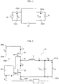
Figure 1 is a schematic illustration of a DC/DCelectronic converter 20. In particular, a genericelectronic converter 20 comprises twoinput terminals output terminals DC voltage source 10, such as a battery, or may be obtained from an AC voltage by means of a rectifier circuit, such as a bridge rectifier, and possibly a filtering circuit. Instead, the output voltage Vout may be used to supply aload 30. -
Figure 2 shows the circuit schematic of an example of abuck converter 20. In particular, abuck converter 20 comprises twoinput terminals output terminals - In the example considered, the
buck converter 20 comprises two electronic switches Q1 and Q2 (with the current path thereof) connected (e.g., directly) in series between theinput terminals terminal 200a and the switching node Lx, and the electronic switch Q2 is a low-side switch connected (e.g., directly) between the switching node Lx and the (negative)terminal 200b, which often represents a ground GND. The (high-side) switch Q1 and the (low-side) switch Q2 hence represent a half-bridge configured to connect the switching node Lx to theterminal 200a (voltage Vin ) or theterminal 200b (ground GND). - In the example considered, an inductance L, such as an inductor, is connected (e.g., directly) between the switching node Lx and the (positive)
output terminal 202a. Instead, the (negative)output terminal 202b is connected (e.g., directly) to the (negative)input terminal 200b. - In the example considered, to stabilize the output voltage Vout, the
converter 20 typically comprises a capacitor Cout connected (e.g., directly) between theoutput terminals - In this context,
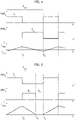
Figure 3 shows exemplary waveforms of the signals of such an electronic converter, where: -
Figure 3a shows the signal DRV1 for switching the electronic switch Q1; -
Figure 3b shows the signal DRV2 for switching the second electronic switch Q2; -
Figure 3c shows the current IQ1 that traverses the electronic switch Q1; -
Figure 3d shows the voltage VLx at the switching node Lx (i.e., the voltage at the second switch Q2); and -
Figure 3e shows the current IL that traverses the inductor L. - In particular, when the electronic switch Q1 is closed at an instant t 1 (ON state), the current IL in the inductor L increases (substantially) linearly. The electronic switch Q2 is at the same time opened. Instead, when the electronic switch Q1 is opened after an interval TON1 at an instant t 2 (OFF state), the electronic switch Q2 is closed, and the current IL decreases (substantially) linearly. Finally, the switch Q1 is closed again after an interval TOFF1. In the example considered, the switch Q2 is hence closed when the switch Q1 is open, and vice versa. The current IL may thus be used to charge the capacitor Cout, which supplies the voltage Vout at the
terminals - In the example considered, the
electronic converter 20 comprises thus acontrol circuit 22 configured to drive the switching of the switch Q1 and of the switch Q2, for repeating the intervals TON1 and TOFF1 periodically. For example, typically thebuck converter 20 comprises also afeedback circuit 24, such as a voltage divider, configured to generate a feedback signal FB indicative of (and preferably proportional to) the output voltage Vout, and thecontrol circuit 22 is configured to generate the drive signals DRV1 and DRV2 by comparing the feedback signal FB with a reference signal, such as a reference voltage Vref. - A significant number of driving schemes are known for generating the drive signals DRV1 and DRV2. These solutions have in common the possibility of regulating the output voltage Vout by regulating the duration of the interval TON1 and/or the interval TOFF1.
- For example, in various solutions, the
control circuit 22 generates a Pulse-Width Modulation (PWM) signal DRV1, wherein the duty-cycle TON1 /(T ON1 + TOFF1 ) is variable. Generally, the switching period Tsw = TON1 + TOFF1 may be constant or variable. For example, a typical control scheme involves that the switching period Tsw is constant and the duration of the interval TON1 is varied via a regulator circuit having at least an integral component, such as a PI (Proportional-Integral) or PID (Proportional-Integral-Derivative) regulator. - In general, a buck converter may be operated in a Continuous-Conduction Mode (CCM), Discontinuous-Conduction Mode (DCM) or Transition Mode (TM).
- For example, as shown in
Figure 4 , when thecontrol circuit 22 operates the converter in CCM, the current IL flowing through the inductance L has a value different from zero when the switching cycle Tsw ends. In this case, thecontrol circuit 22 uses two switching phases T1 and T2 , with Tsw = T1 + T2, wherein: - during the phase T1 (T1 = TON1 = TOFF2 ) the switch Q1 is closed and the switch/diode Q2 is opened; and
- during the phase T2 (T2 = TOFF1 = TON2 ) the switch Q1 is opened and the switch/diode Q2 is closed.
- Conversely, as shown in
Figure 5 , in DCM, thecontrol circuit 22 may use three switching phases T1 , T2 and T3 , with Tsw = T1 + T2 + T3 , wherein: - during the phase T1 (T1 = TON1 ) the switch Q1 is closed and the switch/diode Q2 is opened;
- during the phase T2 (T2 = TON2 ) the switch Q1 is opened and the switch/diode Q2 is closed; and
- during the phase T3 (TOFF1 = T2 + T3 and TOFF2 = T3 + T1 ) the switch Q1 is opened and the switch/diode Q2 is opened.
- Specifically, in DCM, the electronic switch Q2 is opened (and remains opened during the interval T3 ) when the current IL reaches zero.
- In various solutions, also (usually fixed) dead times may be introduced between the switching of the drive signals, e.g., between the falling edge of the signal DRV1 and the rising edge of the signal DRV2 , and similarly (in CCM mode) between the falling edge of the signal DRV2 and the rising edge of the signal DRV1. Insofar as these intervals are usually short compared to the durations TON and TOFF , these intervals will not be considered specifically in the following.
- For higher current flows, the buck converter may also be used as in a multiphase configuration, so called multiphase buck converters. Specifically, in this case a plurality of buck converters are used to charge the same output capacitor Cout, wherein each buck buck converter represents a phase of the multiphase buck converters.
- Considering the foregoing, various embodiments of the present disclosure relate to improvements within multiphase buck converters.
- According to one or more embodiments, one or more of the foregoing objects are achieved by means of a control circuit for a multiphase buck converter having the distinctive elements specified in the ensuing claims. Embodiments also regard a corresponding integrated circuit, multiphase buck converter and method of operating a multiphase buck converter.
- The claims form an integral part of the technical teaching according to the description provided herein.
- As mentioned before, various embodiments of the present disclosure relate to a control circuit for a multiphase buck converter.
- For example, as will be described in greater detail in the following, such a multiphase buck converter may comprise a first and a second input terminal configured to receive an input voltage, and a first and a second output terminal configured to provide the output voltage. In this case, one or more capacitors may be connected between the first and the second output terminals, and a feedback circuit generates a feedback signal indicative of the output voltage. Moreover, the multiphase buck converter comprises a plurality of stages. Specifically, in various embodiments, each stage comprises an inductance, wherein a first terminal of the inductance is connected to the first output terminal. Moreover, a first electronic switch and either a second electronic switch or a diode are connected between the first and the second input terminals and are configured to selectively connect a second terminal of the inductance to the first input terminal or the second input terminal. In various embodiments, a driver circuit of the stage is configured to receive a respective PWM signal and generate a respective first drive signal for the first electronic switch, and optionally a respective second drive signal for the second electronic switch (if provided). Moreover, a current sensor is configured to generate a respective current sense signal indicative of the current flowing through the respective inductance.
- Accordingly, in various embodiments, the control circuit comprises a feedback terminal configured to receive the feedback signal indicative of the output voltage generated by the multi-phase buck converter. Similarly, the control circuit comprises a plurality of current-sense terminals, wherein each current-sense terminal is configured to receive from a respective stage of the multiphase buck converter a respective current sense signal indicative of the current flowing through the inductance of the respective stage. Finally, the control circuit comprises a plurality of control terminals, wherein the number of the control terminals corresponds to the number of the current-sense terminals, wherein each control terminal is configured to provide a respective PWM signal to the driver circuit of a respective stage of the multiphase buck converter. Thus, in general, each PWM signal is associated with a respective stage and thus with a respective current sense signal.
- In various embodiments, the driver circuits may also be integrated in the control circuit, i.e., the control circuit may comprise a plurality of driver circuits, wherein the number of the driver circuits corresponds to the number of the control terminals, and wherein each driver circuit is configured to receive a respective PWM signal and generate a respective first drive signal for the first electronic switch of the respective stage, and optionally the respective second drive signal for the second electronic switch of the respective stage (if provided).
- Accordingly, in various embodiments, the control circuit is configured to generate the PWM signals as a function of the feedback signal and the current sense signals.
- For example, in various embodiments, the control circuit comprises a regulator circuit configured to generate a regulation signal by varying the regulation signal until the feedback signal corresponds to a reference signal. For example, the regulator circuit may be a (digital or analog) regulator comprising an integral component, and optionally a proportional and/or derivative component.
- In this case, the control circuit comprises moreover a plurality of phase control circuits, wherein each phase control circuit is configured to receive a respective current sense signal and generate a respective PWM signal by varying the duty-cycle of the respective PWM signal as a function of the respective current sense signal and the regulation signal generated by the regulator circuit. For example, a phase control circuit may comprise a comparator configured to signal the end of a switch-on interval of the respective PWM signal when the instantaneous value of the respective current sense signal reaches the regulation signal during the switch-on interval, whereby the regulation signal represents a threshold value for the instantaneous current. Alternatively, a phase control circuit may comprise a further regulator having an integral component and/or a proportional component, and configured to vary the duty-cycle of the respective PWM signal as a function of the difference between the average value during the switch-on interval of the respective current sense signal and the regulation signal, whereby the regulation signal represents a reference value for the average current.
- Specifically, in various embodiments, the control circuit comprises moreover a first selector circuit and a second selector circuit configured to receive a selection signal and, in response to the selection signal, selectively connect each phase control circuit of a subset of a given number of phase control circuits, via a respective second PWM signal, to one of the PWM signals and, via a respective second current sense signal, to the current sense signal associated with the PWM signal connected to the phase control circuit, i.e., the current sense signal associated with the PWM signal connected to the respective second PWM signal. For example, the first selector circuit may comprise a plurality of electronic switches for connecting each second current sense signal to each current sense signal, and the second selector circuit may comprise a plurality of electronic switches for connecting each second PWM signal to each PWM signal.
- In various embodiments, a selection control circuit may thus be configured to generate the selection signal. Specifically, in a first switching mode, the selection control circuit may set the selection signal in order to connect the given number of phase control circuits to a first set of PWM signals and associated current sense signals. Conversely, in a second switching mode, the selection control circuit may set the selection signal in order to connect the given number of phase control circuits to a second set of PWM signals and associated current sense signals, wherein the second set is at least in part different from the first set.
- For example, the number of phase control circuits in the subset may correspond to the number of activated phase control circuits. For example, for this purpose, the regulator circuit may be configured to determine, as a function of the regulation signal, a number of phase control circuits to be activated, and activate the corresponding number of phase control circuits.
- In general, the number of phase control circuits may thus correspond to or may be smaller than the number of stages of the multiphase buck converter (as indicated, e.g., by the number of the current-sense terminals).
- Generally, the selection control circuit may use different solutions for selecting the subset of stages to be connected to the phase control circuits.
- For example, in various embodiments, the control circuit comprises a communication interface, and the selection control circuit is configured to activate the first switching mode or the second switching mode as a function of a control signal received via the communication interface. In this case, the selection control circuit may be configured to select the stages belonging to the first subset of stages (i.e., the respective first set of PWM signals and associated current sense signals) and/or the second subset of stages (i.e., the respective second set of PWM signals and associated current sense signals) as a function of the control signal received via the communication interface.
- Additionally or alternatively, the selection control circuit may be configured to activate the first switching mode and monitor the respective first subset of current sense signals of the respective stages connected to the phase control circuits. Next, the selection control circuit may determine whether a monitored current sense signal is greater than an upper threshold (e.g., indicative of a short-circuit condition) and/or smaller than a lower threshold (e.g., indicative of an open-load condition), and possibly activate the second switching mode, wherein the second set of stages (i.e., the respective set of current sense signals and PWM signals) does not comprise anymore the monitored stage/current sense signal.
- Additionally or alternatively, the selection control circuit may be configured to periodically activate the first switching mode and the second switching mode.
- The embodiments of the present description will now be described with reference to the annexed drawings, which are provided purely by way of non-limiting example, and in which:
-
Figure 1 shows a typical application of an electronic converter; -
Figure 2 shows an example of a buck converter; -
Figure 3a to 3e show exemplary waveforms of the buck converter ofFigure 2 ; -
Figure 4 shows exemplary waveforms when the buck converter is operated in CCM; -
Figure 5 shows exemplary waveforms when the buck converter is operated in DCM; -
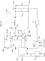
Figure 6 shows an embodiment of a control circuit for a single-stage buck converter; -
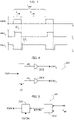
Figure 7 shows an embodiment of the generation of the drive signals for the electronic switches of a buck converter as a function of a PWM signal; -
Figure 7 shows an embodiment of a driver circuit configured to generate the drive signals for the electronic switches of a buck converter as a function of a PWM signal; -
Figure 9 shows an embodiment of a regulator circuit configured to generate a PWM signal as a function of a feedback signal of the buck converter; -
Figure 10 shows an embodiment of a multi-phase buck converter; -
Figure 11 shows an embodiment of a regulator circuit configured to generate PWM signals for the multi-phase buck converter ofFigure 10 ; -
Figure 12 shows an embodiment of the operation of the regulator circuit ofFigure 11 ; -
Figure 13 shows an embodiment of a regulator circuit comprising two switching circuits; -
Figures 14 and 15 show possible embodiments of the switching circuits ofFigure 13 . -
Figure 16 shows an embodiment of a digital implementation of the regulator circuit ofFigure 13 ; and -
Figures 17 and 18 shows possible operations of the regulator circuits ofFigure 13 and16 . - In the ensuing description various specific details are illustrated aimed at enabling an in-depth understanding of the embodiments. The embodiments may be provided without one or more of the specific details, or with other methods, components, materials, etc. In other cases, known structures, materials, or operations are not illustrated or described in detail so that various aspects of the embodiments will not be obscured.
- Reference to "an embodiment" or "one embodiment" in the framework of the present description is intended to indicate that a particular configuration, structure, or characteristic described in relation to the embodiment is comprised in at least one embodiment. Hence, phrases such as "in an embodiment" or "in one embodiment" that may be present in various points of this description, do not necessarily refer to one and the same embodiment. Moreover, particular conformations, structures, or characteristics may be combined in any adequate way in one or more embodiments.
- The references used herein are merely provided for convenience and hence do not define the sphere of protection or the scope of the embodiments.
- In attached
Figures 6 to 18 , parts, elements, or components that have already been described with reference toFigures 1 to 5 are designated by the same references used previously in these figures; the description of these elements described previously will not be repeated hereinafter in order not to overburden the present detailed description. - As mentioned before, various embodiments of the present disclosure relate to a control circuit for a multiphase buck converter.
-
Figure 6 shows in this respect an embodiment of a control circuit for a single-stage buck converter 20a. - As described with respect to
Figure 2 , such abuck converter 20a comprises twoinput terminals output terminals - In the embodiment considered, the
buck converter 20a comprises two electronic switches Q1 and Q2 (with the current path thereof) connected (e.g., directly) in series between theinput terminals - In the embodiment considered, an inductance L, such as an inductor, is connected (e.g., directly) between the switching node Lx and the (positive)
output terminal 202a. Instead, the (negative)output terminal 202b is connected (e.g., directly) to the (negative)input terminal 200b. - In the embodiment considered, the
converter 20a typically comprises a capacitor Cout connected (e.g., directly) between theoutput terminals - Specifically, in
Figure 6 , thebuck converter 20a comprises also: - a
feedback circuit 24 configured to generate a feedback signal FB indicative of (and preferably proportional to) the output voltage Vout; and - a
control circuit 22a configured to generate the drive signal DRV1 for the electronic switch Q1 and optionally the drive signal DRV2 for the electronic switch Q2 (in case the electronic switch Q1 is not replaced with a diode) as a function of the feedback signal FB and a reference signal Vref indicative of (and preferably proportional to) a requested value for the output voltage Vout. - Specifically, in
Figure 6 , thecontrol circuit 22a comprises: - a PWM
signal generator circuit 222 configured to generate a Pulse-Width Modulated (PWM) signal PWM as a function of the feedback signal FB and the reference signal Vref ; and - a
driver circuit 220 configured to generate the drive signal DRV1 for the electronic switch Q1 and optionally the drive signal DRV2 for the electronic switch Q2 as a function of the PWM signal PWM - Generally, as shown in
Figure 7 , the PWM signal PWM comprises a switch-on period TON where the signal is set to high and a switch-off period TOFF where the signal is set to high. Generally, the switching period Tsw = TON + TOFF , may be constant or variable. -
Figure 8 shows a possible embodiment of thedriver circuit 220. - Specifically, in case the buck-
converter 20a comprises the electronic switch Q1 and a diode D, thedriver circuit 220 may comprise a high-side driver circuit 2202 configured to generate the drive signal DRV1 as a function of the PWM signal PWM Specifically, in this case, the high-side driver circuit 2202 may receive at input a signal IN1 , which corresponds to the signal PWM, i.e., the logic level of the drive signal DRV1 corresponds to the logic level of the PWM signal PWM, but the signal levels change in order to correctly drive the high side switch Q1, possibly also implementing a slew-rate control. - Conversely, in case the buck-
converter 20a comprises the electronic switch Q1 and the electronic switch Q2, thedriver circuit 220 may comprise: - a high-
side driver circuit 2202 configured to generate the drive signal DRV1 as a function of a signal IN1 ; - a low-
side driver circuit 2204 configured to generate the drive signal DRV2 as a function of a signal IN2 ; and - a driver control circuit 2200 configured to generate the signals IN1 and IN2 for the high-
side driver circuit 2202 and low-side driver circuit 2204 as a function of the PWM signal PWM - Specifically, as shown in
Figure 7 , thedriver control circuit 2220 may be configured to monitor the rising and falling edged of the PWM signal PWM and: - in response to detecting a rising edge, set the signal IN2 /DRV2 (e.g., immediately) to low and set the signal IN1 /DRV1 (immediately or preferably after a dead-time DT1 ) to high; and
- in response to detecting a falling edge, set the signal IN1 /DRV1 (e.g., immediately) to low and set the signal IN2 /DRV2 (immediately or preferably after a dead-time DT2 ) to high.
- As mentioned before, this driving scheme may be used when the buck-
converter 20a is driven in CCM. Conversely, in DCM, the electronic switch Q2 (when used) should be opened when the current flowing through the inductance L reaches zero during the switch-off period TOFF. For example, for this purpose, thedriver circuit 220 may also receive a so called zero current signal ZC indicating whether the current IL flowing through the inductance L reaches zero (at least during the interval TOFF ). Accordingly, in this case, thedriver control circuit 2220 may be configured to monitor the rising and falling edged of the PWM signal PWM and the zero-current signal ZC, and: - in response to detecting a rising edge, set the signal IN1 /DRV1 (e.g., immediately) to high; and
- in response to detecting a falling edge, set the signal IN1 /DRV1 (e.g., immediately) to low and set the signal IN2 /DRV2 (immediately or preferably after a dead-time DT2 ) to high; and
- in response to detecting that the zero-current signal ZC indicates that the current flowing through the inductance L reaches zero during the switch-off period TOFF , set the signal IN2 /DRV2 (e.g., immediately) to low.
- For example, as shown in
Figure 6 , the zero-current signal ZC may be provided by a zerocurrent detection circuit 224. For example, the zerocurrent detection circuit 224 may be implemented with a comparator, so called zero-current comparator, receiving at input a signal indicative of the current IL flowing through the inductance L during the switch-off period TOFF. Specifically, the zero-current comparator may be configured to determine whether the monitored signal falls below a given threshold (which is usually close to zero). - For example, as shown in
Figure 6 , thebuck converter 20a may comprise acurrent sensor 26 connected directly in series with the inductance L, wherein thecurrent sensor 26 provides a signal CS indicative of (and preferably proportional to) the current IL flowing through the inductance L. - Alternatively, the current IL flowing through the inductance L during the switch-off period TOFF may be monitored via a
current sensor 26b connected directly in series with the electronic switch Q2, wherein thecurrent sensor 26b provides a signal CSb indicative of (and preferably proportional to) the current flowing through the switch Q2, which corresponds to the current IL flowing through the inductance L during the interval TOFF. - Accordingly, the zero-
current comparator 224 may receive the signal CS or CSb. - In order to generate the PWM signal PWM, the
PWM generator circuit 222 may use various solutions. Generally, these solutions have in common that, irrespective of whether CCM or DCM is used, the energy transfer may be regulated by varying the duty-cycle of the PWM signal DRV. - For example, in a first embodiment, the
PWM generator circuit 222 is configured to directly vary the duty-cycle of the PWM signal PWM, e.g.: - increase the duty-cycle of the PWM signal PWM when the feedback signal FB is smaller than the reference signal Vref ; and
- decrease the duty-cycle of the PWM signal PWM when the feedback signal FB is greater than the reference signal Vref.
- For example, for this purpose, the PWM generator circuit comprise a regulator having at least an integral component I, such as a PI o PID regulator, configured to vary the duty-cycle of the PWM signal PWM as a function of the error, i.e., the difference, between the signals FB a Vref. Generally, the PWM generator circuit may vary the duty-cycle of the signal PWM by:
- using a constant switching period Tsw, and varying the switch-on period TON ;
- using a constant switch-on period TON , and varying the switching period TSW ; or
- varying both the switching period TSW and the switch-on period TON.
- Conversely, as will be described in greater detail in the following, in a multi-phase buck converter, it is preferable to generate the PWM signal PWM rather based on the current flowing through the inductance L. For example, in this way may be balanced the current flows in the various stages.
- Accordingly, in a second solution, the
PWM generator circuit 222 may be configured to monitor a signal indicative of the average value of the current IL flowing through the inductance L during the switch-on period TON. For example, this is shown inFigure 6 , where thePWM generator circuit 222 receives the signal CS provided by thesensor 26. - Alternatively, the current IL flowing through the inductance L during the switch-on period TON may be monitored via a
current sensor 26a connected directly in series with the electronic switch Q1, wherein thecurrent sensor 26a provides a signal CSa indicative of (and preferably proportional to) the current flowing through the switch Q1, which corresponds to the current IL flowing through the inductance L during the interval TON. - Specifically, as shown in
Figure 9 , in this case, thePWM generator circuit 222 may comprise: - a first regulator 2220 (inner loop) having at least an integral component I and/or a proportional component P, such as a PI o PID regulator, configured to vary the duty-cycle of the PWM signal PWM as a function of a first error, in particular the difference between the average value of the current IL flowing through the inductance L during the interval TON and a reference value REF; and
- a second regulator 2222 (outer loop) having at least an integral component I, such as a PI o PID regulator, configured to vary the reference value REF as a function of a second error, in particular the difference between the feedback signal FB and the reference signal Vref.
- Alternatively, the
PWM generator circuit 222 may be configured to monitor a signal indicative of the instantaneous value of the current IL flowing through the inductance L during the switch-on period TON. For example, for this purpose may be used thecurrent sensor 26 or thecurrent sensor 26a. - Specifically, in this case, the
PWM generator circuit 222 may comprise: - a
comparator 2220 configured to signal the end of the switch-on interval TON when the instantaneous value of the current IL flowing through the inductance L during the interval TON reaches a threshold value TH; and - a
regulator 2222 having at least an integral component I, such as a PI o PID regulator, configured to vary the threshold value TH as a function of an error, in particular the difference, between the feedback signal FB and the reference signal Vref. - Thus, in various embodiments, the regulation of the
buck converter 20a may also take into account the instantaneous and/or average value of the current IL during the interval TON and/or TOFF. - For example, the current sensors shown in
Figure 6 may be implemented with a shunt resistor, where the voltage across the shunt resistor is proportional to the current that traverses the resistor. Alternatively, it is possible to use (for the sensor 26) the DC resistance (DCR) of the inductance L or (for thesensors 26a/26b) the resistance of the switch Q1/Q2, for example the on-state resistance RDS,on (resistance between the drain and source terminals in the ON state), e.g., of a respective MOSFET. Other possible embodiments of current sensors adapted to be used to monitor instantaneous and/or average current flows in a buck converter are, e.g., disclose inItalian patent application n. 102020000028832 -
Figure 10 shows an embodiment of a multiphase buck converter that comprises n phases/stages 201, ..., 20n. - Substantially, each phase has the structure illustrated in
Figure 6 , with the only difference that all the stages charge the same capacitor Cout (or a plurality of capacitors connected in parallel). Consequently, eachstage 201, ..., 20n comprises a respective switch Q1 and a respective switch Q2/diode D, where the switching node Lx is connected via a respective inductor L1, ..., Ln to the terminal 202a, where the switch Q1 and optionally the switch Q2 are driven by means of arespective driver circuit 220 configured to generate the drive signal DRV1 and optionally the drive signal DRV2 as a function of a respective PWM modulated signal PWM1 , ..., PWMn, and optionally a zero current signal ZC. - In the embodiment considered, a
PWM generator circuit 222a may thus vary the duty-cycles of the PWM modulated signals PWM1 , ..., PWMn provided to thestages 201, ..., 20n in such a way that the signal FB provided by thefeedback circuit 24 corresponds to the threshold Vref. In various embodiments, thePWM generator circuit 222 may also monitor for eachstage 201, ..., 20n a signal indicative of the current CS1 , ..., CSn flowing through the respective inductance L1, ..., Ln, such as the signal CS provided by thesensor 26 or the signal CSa provided by thesensor 26a. - Thus, essentially, each
stage 201, ..., 20n comprises: - an electronic switch Q1, and an electronic switch Q2 or diode D;
- a respective inductance L1, ..., Ln;
- a current sensor providing a respective signal CS1 , ..., CSn indicative of (and preferably proportional to) the (instantaneous or average value of the) current IL flowing through the respective inductance L1, ..., Ln;
- a
driver circuit 220 configured to generate the drive signal DRV1 for the electronic switch Q1 and optionally the drive signal DRV2 for the electronic switch Q2 as a function of a PWM modulated signal; and - optionally, in in case the stage comprises also the electronic switch Q2 and may be operated in DCM, a respective zero-
current detection circuit 224. - Conversely, the following circuits are common for the multiphase buck converter:
- the output capacitor(s) Cout;
- the
feedback circuit 24; and - the
PWM generator circuit 222a configured to generate the PWM modulated signals PWM1 , ..., PWMn as a function of the feedback signal FB, the reference signal Vref , and the signals CS1 , ..., CSn provide by thestages 201, ..., 20n. - For example, as shown in
Figure 11 , in various embodiments, thePWM generator circuit 222a may comprise: - for each
stage 201, ..., 20n, a respective phase control circuit, such as:- a
regulator 22201, ..., 2220n (inner loop) having at least an integral component I and/or a proportional component P, such as a PI o PID regulator, configured to vary the duty-cycle of the PWM signal PWM as a function of the error, i.e., the difference, between the average value of the current IL flowing through the respective inductance L1, ..., Ln during the respective switch-on interval TON1 , ..., TONn and a given reference value REF, or - a
comparator 22201, ..., 2220n configured to signal the end of the respective switch-on interval TON1 , ..., TONn when the instantaneous value of the current IL flowing through the respective inductance L1, ..., Ln during the respective interval TON1 , ..., TONn reaches a given threshold value TH; and
- a
- a
common regulator circuit 2222 having at least an integral component I, such as a PI o PID regulator, configured to vary the reference value REF or the threshold value TH, respectively, as a function of the error, i.e., the difference, between the signals FB and the reference signal Vref. - Accordingly, in various embodiments, the
PWM generator circuit 222a is configured to generate a common regulation signal REF or TH for the (average or instantaneous value of the) currents flowing in thestages 201, ..., 20n in order to obtain a requested output voltage Vout, but the current flow in each stage may be controlled individually. For example, in this way may be balanced the currents flowing in the various stages to the same value. - As shown in
Figure 12 , in various embodiments, thePWM generator circuit 222a, in particular thecircuits 22201, ..., 2220n, may be configured to generate PWM signals PWM1 , ..., PWMn having the same switching period Tsw, wherein the respective switch-on period TON1 , ..., TONn is controlled via therespective circuit 22201, ..., 2220n. In various embodiments, in various embodiments, thePWM generator circuit 222a, in particular thecircuits 22201, ..., 2220n, may be configured to generate phase-shifted PWM signals PWM1 , ..., PWMn. For example, in this way also the current peaks supplied by thevarious stages 201, ..., 20n are phase-shifted with respect to each other. - In various embodiments, the
circuit 2222 may also be configured to determine a number k of stages that are to be used, whereas the other n - k stages do not switch. For example, thecircuit 2222 may be configured to: - reduce the number k when the reference value REF or the threshold value TH falls below a lower threshold; and
- increase the number k when the reference value REF or the threshold value TH exceeds an upper threshold.
- Generally, the lower threshold and upper threshold may also be different for each value of k.
- In the embodiment shown in
Figure 10 , the inductors L1, ..., Ln and the capacitor or capacitors Cout are represented as being external to thestages 201, ..., 20n to highlight the fact that thestages 201, ..., 20n and possibly thePWM generator circuit 222, thedriver circuits 220 and optionally the electronic switches Q1 and Q2 may be implemented in one or more integrated circuits, whereas the inductors L1, ..., Ln and the capacitor or capacitors Cout may be discrete components connected externally to such one or more integrated circuits. - Generally, also other control schemes may be implemented in the PWM generator circuit in order to generate the PWM signals PWM1 , ..., PWMn. For example, an alternative solution is described in document "
DocID030464 Rev 1", "TN1246 Technical note: Digital multiphase constant-on-time regulator based on voltage controlled oscillator", STMicroelectronics, 2017. A modified multiphase buck converter with the possibility of zero-voltage switching is described in U.S. patent application No.US 2019/0052165 A1 , the contents of which are incorporated herein for reference. - Accordingly, a multiphase buck converter comprises a plurality of phases, wherein each phase may provide a current pulse to the output capacitor(s) Cout. Moreover, by using PWM signals PWM1 , ..., PWMn , the current pulses may be phase shifted and the current in the phases may be balanced. Generally, as mentioned before, based on the load conditions, also only a sub-set of k phases may indeed be used.
-
Figure 13 shows an embodiment of a modifiedcontrol circuit 22b for a multi-phase buck converter having n phases/stages. For example, such acontrol circuit 22b may be implemented in an integrated circuit. - Specifically, in line with the previous description, the
control circuit 22b comprises: - a terminal configured to receive the feedback signal FB indicative of (and preferably proportional to) the output voltage Vout generated by the multi-phase buck converter,
- n terminals configured to receive from each stage a respective current sense signal CS1 , ..., CSn indicative of (and preferably proportional to) the current flowing through the inductance of the respective stage;
- n terminals configured to provide a PWM signal PWM1 , ..., PWMn to the
driver circuit 220 of the respective stage. - In various embodiments, the
control circuit 22b may also comprises a terminal configured to receive the reference signal V ref indicative of (and preferably proportional to) the requested value of the output voltage generated by the multi-phase buck converter. - In various embodiments, as shown in
Figure 13 , the integrated circuit of thecontrol circuit 22b may also comprise for each stage arespective driver circuit 2201, ..., 220n. Generally, as described in the foregoing, eachdriver circuit 2201, ..., 220n is configured to generate, as a function of the respective PWM signal PWM1 , ..., PWMn, a drive signal DRV1 , for an electronic switch Q1 of the respective stage, and optionally a drive signal DRV2 for an electronic switch Q2 of the respective stage. - Accordingly, in various embodiments, the integrated circuit of the
control circuit 22b may comprise pads of a respective die or pins of a respective packaged integrated circuit for the feedback signal FB, the signal CS1 , ..., CSn, optionally the reference signal Vref, and either: - for the PWM signal PWM1 , ..., PWMn ; or
- for the drive signal DRV1 and optionally the drive signal DRV2.
- In various embodiments, also the electronic switches Q1 and the electronic switches Q2/diodes D may be integrated in the integrated circuit. Accordingly, in this case, the signals CS1 , ..., CSn could be generated internally, e.g., by monitoring the voltages at the switching nodes Lx.
- In the embodiment considered, the
control circuit 22b comprises again aregulator circuit 2222 configured to generate a regulation value REG by varying the regulation value REG until the feedback signal FB corresponds to the reference signal Vref. As mentioned before, theregulator circuit 2222 may comprise at least an integral component (I), and optionally a proportional (P) and/or derivative (D) component. - Moreover, in the embodiment considered, the
control circuit 22b comprises nphase control circuits 22201, ..., 2220n (one for each stage/phase) configured to generate a respective PWM signal PWM1 , ..., PWMn by varying the duty-cycle of the respective PWM signal PWM1 , ..., PWMn as a function of the respective current sense signal CS1 , ..., CSn and the regulation value REG. For example, the regulation value REG may correspond to the reference value REF of the average value of the current sense signal CS1 , ..., CSn or the threshold value for the instantaneous value of the current sense signal CS1 , ..., CSn. Accordingly, eachcontrol circuits 22201, ..., 2220n may be implemented with a respective comparator or an additional regulator having a P and/or I component. - Specifically, as shown in
Figure 13 , indeed each of the nphase control circuits 22201, ..., 2220n receives a respective current sense signal CS'1, ..., CS'n and generates a respective PWM signal PWM'1 , ..., PWM'n. In fact, in the embodiment considered, thecontrol circuit 22b comprises also: - a
first selector circuit 30 configured to select for each current sense signal CS'1 , ..., CS'n a respective current sense signal CS1 , ..., CSn as a function of a selection signal SEL, and - a
second selector circuit 32 configured to select for each PWM signal PWM1 , ..., PWMn a respective PWM signal PWM'1 , ..., PWM'n as a function of the selection signal SEL. - Thus, in the embodiment considered, each couple of current sense signal CS1 , ..., CSn and PWM signal PWM1 , ..., PWMn (associated with a given phase/stage) may be routed via the
selector circuits respective control circuit 22201, ..., 2220n. - In various embodiments, the
control circuit 22b comprises thus also aselection control circuit 34 configured to generate the selection signal SEL for theselector circuits - For example, the
selector circuits control circuit 22201, ..., 2220n may also be unused. In this case, theselector circuits unused control circuit 22201, ..., 2220n. - For example,
Figures 14 and 15 show possible embodiment of theselector circuit - Specifically, in the embodiment considered, each current sense signal CS'1, ..., CS'n is connected via a respective electronic switch to all current sense signals CS1 , ..., CSn, e.g., electronic switches SC11, SC12 and SC13 for connecting the current sense signal CS'1 to the current sense signals CS1 , CS2, CS3, electronic switches SC21, SC22 and SC23 for connecting the current sense signal CS'2 to the current sense signals CS1 , CS2, CS3, etc.
- Similarly, in the embodiment considered, each PWM signal PWM'1 , ..., PWM'n is connected via a respective electronic switch to all PWM signals PWM1 , ..., PWMn, e.g., electronic switches SP11, SP12 and SP13 for connecting the PWM signal PWM'1 to the PWM signal signals PWM1 , PWM2, PWM3, electronic switches SP21, SP22 and SP23 for connecting the PWM signal PWM'2 to the PWM signal signals PWM1 , PWM2, PWM3 , etc.
- Accordingly, in the embodiment considered, the selection signal SEL may be a one-hot encoded signal, which closes for each current sense signal CS1 , ..., CSn and each PWM signal PWM'1 , ..., PWM'n just one electronic switch. For example, in
Figures 14 and 15 , the current sense signal CS1 and the PWM signals PWM1 are connected to thephase control circuit 22201, the current sense signal CS3 and the PWM signal PWM3 are connected to thephase control circuit 22202, and the current sense signal CS2 and the PWM signal PWM2 are disconnected. - Generally, as shown in
Figure 16 , at least part of thecontrol circuit 22b may also be implemented via a digital processing circuit, e.g., comprising a dedicated hardware circuit and/or a micro-processor configured to implement one or more operations of thecontrol circuit 22a via software instructions. - For example, in
Figure 16 , thecontrol circuit 22b comprises one or more analog-to-digital converters ADCS configured to generate digital samples CSD1 , ..., CSD2 of the current sense signal CS1 , ..., CSn. Similarly, thecontrol circuit 22b may comprises an analog-to-digital converters ADFB configured to generate a digital sample of the feedback signal FB. For example, in a digital implementation, thecontrol circuit 22b may comprise a communication interface IF for receiving the reference signal Vref. Accordingly, in general, thecircuits - In the following will now be described possible embodiments of the
selection control circuit 34. - For example, in various embodiments, which may be particularly suitable in case the
control circuit 22b comprises also a communication interface IF, such as a serial communication interface, e.g., an I2C (Inter-Integrated Circuit) or SPI (Serial Peripheral Interface Bus) communication interface, theselection control circuit 34 may be configured to use a predetermined assignment for the connection of the current sense signal CS1 , ..., CSn and the PWM signals PWM1 , ..., PWMn to thephase control circuits 22201, ..., 2220n. For example, the predetermined assignment may be received via the communication interface IF. - For example, with respect to
Figure 14 and 15 , theselection control circuit 34 may receive via the communication interface IF data specifying that: - the current sense signal CS1 and the PWM signals PWM1 are connected to the
phase control circuit 22201, - the current sense signal CS3 and the PWM signal PWM3 are connected to the
phase control circuit 22202, and - the current sense signal CS2 and the PWM signal PWM2 is disconnected.
- For example, in various embodiments, the data may correspond to the bit sequence of the selection signal SEL, e.g., "100 001 000" or an encoded sequence "01 11 00", i.e., corresponding to the decimal values "1,3,0", which is decoded by the
selection control circuit 34 in order to generate the selection signal SEL. - In various embodiments, the
control circuit 22b may use only kphase control circuits 22201, ..., 2220n. For example, as described in the foregoing, theregulator circuit 2222 may vary the number k based on the required load conditions. Accordingly, in various embodiments, the number k of activephase control circuits 22201, ..., 2220n is smaller than the number n of phases of the multiphase buck converter. - For example, this is also shown in
Figures 13 and16 , where theselection control circuit 34 receives the value k from theregulator circuit 2222. - Specifically, in this case, the
selection control circuit 34 may drive theselector circuits - compensate a fault of a phase of the multiphase buck converter, by activating a different phase of the multiphase buck converter; and/or
- switch dynamically the activated phases in order to reduce the stress on the activated phases.
- For example, as shown in
Figures 13 and16 , in order to determine a fault of a given phase, theselection control circuit 34 may monitor the current sense signals CS1 , ..., CSn (or the respective digital samples). For example, in case a given phase is activated, i.e., connected to an activatedphase control circuit 22201, ..., 2220n and the respective current sense signals CS1 , ..., CSn has values being too small (open load condition) and/or high (short-circuit condition), the selector circuit may connect a deactivated phase to the respectivephase control circuit 22201, ..., 2220n. - For example, with respect to the embodiment described in the foregoing, wherein the
phases phase control circuit phase 2 is deactivated, i.e., k = 2 (and n is at least 3), theselection control circuit 34 may be configured to: - monitor (at least) the current sense signals CS1 and CS3 ;
- compare the current sense signals CS1 and CS3 with a lower threshold and/or an upper threshold;
- in response to determining that the current sense signal CS1 is smaller than the lower threshold or greater than the upper threshold, set the selection signal SEL in order to deactivate the
phase 1 and connect the previously deactivatedphase 2 to theactive control circuit 22201; and - in response to determining that the current sense signal CS3 is smaller than the lower threshold or greater than the upper threshold, set the selection signal SEL in order to deactivate the
phase 3 and connect the previously deactivatedphase 2 to theactive control circuit 22202; - For example,
Figure 17 shows the example wherein two of three phases are active, i.e., k = 2 and n = 3, and theselection control circuit 34 is configured to: - assign the
phase 1 to thephase control circuit 22201 and thephase 2 to thephase control circuit 22202; - set a respective fault condition signal FC3, FC2, FC3 for each of the
phases 1 to 3, when the respective current sense signals CS1 , ..., CSn indicates a fault; and - in response to determining that the signal FC2 indicates a fault of the
phase 2, vary the selection signal in order to connect thephase 3 to thephase control circuit 22202. - Specifically, as shown in
Figure 17 , due to the fact that thephase control circuit 22202 is first used for thephase 2 and then for thephase 3, the signal PWM2 and (once activated) the signal PWM3 use the same phase shift. Generally, once having switched to another phase, thephase control circuit 22202 and/or theregulator circuit 2222 may again perform the regulation function in order to obtain the requested output voltage. - For example, in this way, by adding a single deactivated/unused phase, which usually would not be required, the
control circuit 22b may compensate the fault of any of the k activated phases, by disconnecting the phase having a fault and connecting the previously deactivated/unused phase to the phase control circuit previously associated with the phase having a fault. Generally, theselection control circuit 34 could also perform a reordering of all connection of the k phases to the k activatedphase control circuits 22201, ..., 2220n. - In fact, as mentioned before, the
selection control circuit 34 may also be configured to dynamically reorder the active phase. Specifically, as mentioned before, theregulator circuit 2222 may adapt the number k of active phases to the current load condition, e.g., in order to optimize the efficiency of the power conversion. However, in a conventional multiphase converter this may give rise to an overstress on the first phases, which are usually always activated. - Conversely, as shown in
Figure 18 , the phase selection circuit may reorder the phase by periodically connecting different subsets of k phases to the k activatedphase control circuits 22201, ..., 2220n. - For example, in the embodiment shown in
Figure 18 , two of threephase control circuits 22201, ..., 2220n are active, i.e., k = 2 and n = 3. For example, in this case, and assuming that no faults are detected (see, e.g., the description ofFigure 17 ) theselection control circuit 34 may change the selection signal SEL in order to repeat the following operations periodically: - connect the
phases phase control circuits - next connect the
phases phase control circuits - next connect the
phases phase control circuits - Accordingly, various embodiments of the present disclosure may have one or more of the following advantages:
- flexibility is increased, because the external component (the inductances L and optionally the electronic switches Q1 and electronic switches Q2/didoes D) are not bound by constraints in the phase assignment;
- the stress on external components may be reduced, thereby increasing their lifetime and improving the performance of the system;
- the fault management is improved with a minimum number of external component redundancy.
- Of course, without prejudice to the principle of the invention, the details of construction and the embodiments may vary widely with respect to what has been described and illustrated herein purely by way of example, without thereby departing from the scope of the present invention, as defined by the ensuing claims.
- For example, while in the previous description the activated phase control circuits receive (in addition to the regulation signal REG) just one signal from a respective stage of the multi-phase buck converter (i.e., the respective current sense signal), the phase control circuits could also receive further signals from the respective stage, such as a signal indicative of the temperature of the respective stage. In this case, the
selector circuit 32 may also be used to route the additional signals associated with the same stage to a given phase control circuit. - Additionally or alternatively, such additional signals may be used by the
selection control circuit 34 in order determine possible malfunctions of a given stage, such as an overtemperature condition, and possibly connect the respective phase control circuit to another stage.
Claims (14)
- A control circuit (22b) for a multiphase buck converter, comprising:- a feedback terminal configured to receive a feedback signal (FB) indicative of an output voltage (Vout ) generated by said multi-phase buck converter,- a plurality of current-sense terminals, wherein each current-sense terminal is configured to receive from a respective stage of said multiphase buck converter a respective first current sense signal (CS1 , ..., CSn ) indicative of the current flowing through an inductance of the respective stage;- a plurality of control terminals, wherein the number (n) of said control terminals corresponds to the number (n) of said current-sense terminals, wherein each control terminal is configured to provide a respective first Pulse-Width Modulated, PWM, signal (PWM1 , ..., PWMn ) to a driver circuit (220) of a respective stage of said multiphase buck converter, and each first PWM signal (PWM1 , ..., PWMn ) is associated with a respective first current sense signal (CS1 , ..., CSn ),- a regulator circuit (2222) configured to generate a regulation signal (REG) by varying said regulation signal (REG) until said feedback signal (FB) corresponds to a reference signal (Vref );- a plurality of phase control circuits (22201, ..., 2220n), wherein each phase control circuit (22201, ..., 2220n) is configured to receive a respective second current sense signal (CS'1 , ..., CS'n ) and generate a respective second PWM signal (PWM'1 , ..., PWM'n ) by varying the duty-cycle of the respective second PWM signal (PWM'1 , ..., PWM'n ) as a function of the respective second current sense signal (CS'1 , ..., CS'n ) and said regulation signal (REG);- a first selector circuit (30) and a second selector circuit (32) configured to receive a selection signal (SEL) and, in response to said selection signal (SEL), selectively connect each phase control circuit (22201, ..., 2220n) of a subset of a given number (k) of said phase control circuits (22201, ..., 2220n):- via the respective second PWM signal (PWM'1 , ..., PWM'n ) to a first PWM signal (PWM1 , ..., PWMn ), and- via the respective second current sense signal (CS'1 , ..., CS'n ) to the first current sense signal (CS1 , ..., CSn ) associated with the first PWM signal (PWM1 , ..., PWMn ) connected to the respective second PWM signal (PWM'1 , ..., PWM'n ); and- a selection control circuit (34) configured to generate said selection signal (SEL), wherein said selection control circuit (34) is configured to:- in a first switching mode, set said selection signal (SEL) in order to connect said given number (k) of said phase control circuits (22201, ..., 2220n) to a first set of first PWM signals (PWM1 , ..., PWMn ) and associated first current sense signals (CS1 , ..., CSn ), and- in a second switching mode, set said selection signal (SEL) in order to connect said given number (k) of said phase control circuits (22201, ..., 2220n) to a second set of first PWM signals (PWM1 , ..., PWMn ) and associated first current sense signals (CS1 , ..., CSn ).
- The control circuit (22b) according to Claim 1, wherein said regulator circuit (2222) is configured to:- determine, as a function of said regulation signal (REG), a number of phase control circuits (22201, ..., 2220n) to be activated, and- activate said number of phase control circuits (22201, ..., 2220n) to be activated; wherein said given number (k) corresponds to the number of activated phase control circuits (22201, ..., 2220n).
- The control circuit (22b) according to Claim 1 or Claim 2, wherein the number of phase control circuits (22201, ..., 2220n) corresponds to or is smaller than said number (n) of current-sense terminals.
- The control circuit (22b) according to any of the previous claims, wherein said control circuit (22b) comprises a communication interface (IF), and wherein said selection control circuit (34) is configured to activate said first switching mode or said second switching mode as a function of a control signal received via said communication interface (IF).
- The control circuit (22b) according to Claim 4, wherein said selection control circuit (34) is configured to select said first set of first PWM signals (PWM1 , ..., PWMn ) and associated first current sense signals (CS1 , ..., CSn ) and/or said second set of first PWM signals (PWM1 , ..., PWMn ) and associated first current sense signals (CS1 , ..., CSn ) as a function of said control signal received via said communication interface (IF).
- The control circuit (22b) according to any of the previous claims, wherein said selection control circuit (34) is configured to:- activate said first switching mode and monitor said first subset of first current sense signals (CS1 , ..., CSn ) connected to said given number (k) of said phase control circuits (22201, ..., 2220n);- determine whether a monitored first current sense signal (CS1 , ..., CSn ) is greater than an upper threshold and/or smaller than a lower threshold, and- in response to determining that said monitored first current sense signal (CS1 , ..., CSn ) is greater than said upper threshold or smaller than said lower threshold, activate said second switching mode, wherein said second set of first current sense signals (CS1, ..., CSn ) does not comprise said monitored first current sense signal (CS1, ..., CSn ).
- The control circuit (22b) according to any of the previous claims, wherein said selection control circuit (34) is configured to periodically activate said first switching mode and said second switching mode.
- The control circuit (22b) according to any of the previous claims, wherein said first selector circuit (30) comprises a first plurality of electronic switches for connecting each second current sense signal (CS'1 , ..., CS'n ) to each first current sense signal (CS1 , ..., CSn ), and wherein said second selector circuit (30) comprises a second plurality of electronic switches for connecting each second PWM signal (PWM'1 , ..., PWM'n ) to each first PWM signal (PWM1 , ..., PWMn ).
- The control circuit (22b) according to any of the previous claims, comprising:- a plurality of driver circuits (2201, ..., 220n), wherein the number (n) of said driver circuits (2201, ..., 220n) corresponds to the number of said control terminals, and wherein each driver circuit (2201, ..., 220n) is configured to receive a respective PWM signal (PWM1 , ..., PWMn ) and generate a respective first drive signal (DRV1 ) for a first electronic switch (Q1) of the respective stage, and optionally a respective second drive signal (DRV2 ) for a second electronic switch (Q2) of the respective stage.
- The control circuit (22b) according to any of the previous claims, wherein said regulator circuit (2222) is a regulator comprising an integral component (I), and optionally a proportional (P) and/or derivative (D) component.
- The control circuit (22b) according to any of the previous claims, wherein each phase control circuits (22201, ..., 2220n) comprises either:- a comparator configured to signal the end of a switch-on interval (TON ) of the respective second PWM signal (PWM'1 , ..., PWM'n ) when the instantaneous value of the respective second current sense signal (CS'1 , ..., CS'n ) reaches said regulation signal (REG) during said switch-on interval (TON ), whereby said regulation signal (REG) represents a threshold value (TH), or- a further regulator having an integral component and/or a proportional component, and configured to vary the duty-cycle of the respective second PWM signal (PWM'1 , ..., PWM'n ) as a function of the difference between the average value during said switch-on interval (TON ) of the respective second current sense signal (CS'1 , ..., CS'n ) and said regulation signal (REG), whereby said regulation signal (REG) represents a reference value (REF).
- An integrated circuit comprising a control circuit (22b) according to any of the previous claims.
- A multiphase buck converter comprising:- a first (200a) and a second (200b) input terminal configured to receive an input voltage (Vin );- a first (202a) and a second (202b) output terminal configured to provide said output voltage (Vout );- a capacitor (Cout) connected between said first (202a) and said second (202b) output terminals;- a feedback circuit (24) configured to generate a feedback signal (FB) indicative of said output voltage (Vout );- a plurality of stages (20), each stage comprising:- an inductance (L), wherein a first terminal of said inductance (L) is connected to said first output terminal (202a),- a first electronic switch (Q1) and either a second electronic switch (Q2) or a diode connected between said first (200a) and said second (200b) input terminals and configured to selectively connect a second terminal of said inductance (L) to said first input terminal (200a) or said second input terminal (200b),- a driver circuit (220) configured to receive a respective first PWM signal (PWM1 , ..., PWMn ) and generate a respective first drive signal (DRV1 ) for said first electronic switch (Q1), and optionally a respective second drive signal (DRV2 ) for said second electronic switch (Q2), and- a current sensor (26, 26a) configured to generate a respective first current sense signal (CS1 , ..., CSn ) indicative of the current flowing through the respective inductance (L); and- a control circuit (222b) according to any of the previous claims 1 to 11.
- A method of operating a multiphase buck converter via a control circuit according to any of the previous claims 1 to 11, comprising:- in a first switching mode, set said selection signal (SEL) in order to connect said given number (k) of said phase control circuits (22201, ..., 2220n) to a first set of first PWM signals (PWM1 , ..., PWMn ) and associated first current sense signals (CS1 , ..., CSn ), and- in a second switching mode, set said selection signal (SEL) in order to connect said given number (k) of said phase control circuits (22201, ..., 2220n) to a second set of first PWM signals (PWM1 , ..., PWMn ) and associated first current sense signals (CS1 , ..., CSn ).
Applications Claiming Priority (1)
| Application Number | Priority Date | Filing Date | Title |
|---|---|---|---|
| IT102021000011780A IT202100011780A1 (en) | 2021-05-07 | 2021-05-07 | Control circuit for a multiphase buck converter, related integrated circuit, multiphase buck converter, and method for operating a multiphase buck converter |
Publications (1)
| Publication Number | Publication Date |
|---|---|
| EP4087108A1 true EP4087108A1 (en) | 2022-11-09 |
Family
ID=77022055
Family Applications (1)
| Application Number | Title | Priority Date | Filing Date |
|---|---|---|---|
| EP22169183.5A Pending EP4087108A1 (en) | 2021-05-07 | 2022-04-21 | Control circuit for a multiphase buck converter, related integrated circuit, multiphase buck converter and method of operating a multiphase buck converter |
Country Status (3)
| Country | Link |
|---|---|
| US (1) | US12021454B2 (en) |
| EP (1) | EP4087108A1 (en) |
| IT (1) | IT202100011780A1 (en) |
Families Citing this family (4)
| Publication number | Priority date | Publication date | Assignee | Title |
|---|---|---|---|---|
| US20220312568A1 (en) * | 2021-03-25 | 2022-09-29 | Semiconductor Components Industries, Llc | Methods and systems of detecting faults in circuits driving average-current loads |
| US12040693B2 (en) * | 2022-07-25 | 2024-07-16 | Elite Semiconductor Microelectronics Technology Inc. | Control circuit with automatic frequency modulation for DC-DC converter |
| EP4407851A1 (en) * | 2023-01-30 | 2024-07-31 | Infineon Technologies Austria AG | Overcurrent protection method and device |
| US12592639B2 (en) | 2023-12-21 | 2026-03-31 | Power Integrations, Inc. | Self-biasing the input controller in a power converter |
Citations (4)
| Publication number | Priority date | Publication date | Assignee | Title |
|---|---|---|---|---|
| US20080150368A1 (en) * | 2006-12-18 | 2008-06-26 | Decicon, Inc. | Configurable power supply integrated circuit |
| US8610412B2 (en) * | 2010-04-16 | 2013-12-17 | O2Micro Inc. | Controllers, systems and methods for implementing multi-phase control |
| US20150311780A1 (en) * | 2013-03-12 | 2015-10-29 | Alpha And Omega Semiconductor Incorporated | Fault tolerant power supply incorporating intelligent gate driver-switch circuit to provide uninterrupted power |
| US20190052165A1 (en) | 2017-08-09 | 2019-02-14 | Stmicroelectronics S.R.L | Electronic converter and related control method, control circuit and computer-program |
Family Cites Families (6)
| Publication number | Priority date | Publication date | Assignee | Title |
|---|---|---|---|---|
| US6246222B1 (en) * | 2000-08-30 | 2001-06-12 | National Semiconductor Corporation | Switching DC-to-DC converter and conversion method with rotation of control signal channels relative to paralleled power channels |
| US6414470B1 (en) * | 2002-01-22 | 2002-07-02 | Richtek Technology Corp. | Apparatus and method for balancing channel currents in a multi-phase DC-to-DC converter |
| US7023188B1 (en) * | 2004-09-10 | 2006-04-04 | Semiconductor Components Industries, L.L.C. | Method of forming a multi-phase power supply controller |
| US8179116B2 (en) * | 2007-06-08 | 2012-05-15 | Intersil Americas LLC | Inductor assembly having a core with magnetically isolated forms |
| TW201012037A (en) * | 2008-09-10 | 2010-03-16 | Richtek Technology Corp | Control circuit of a multi-phase power converter with constant on-time control and method thereof |
| US11258364B2 (en) * | 2020-04-09 | 2022-02-22 | High Tech Technology Limited | Flexible array of DC-DC converters reconfigurable using a shared serial bus |
-
2021
- 2021-05-07 IT IT102021000011780A patent/IT202100011780A1/en unknown
-
2022
- 2022-04-21 EP EP22169183.5A patent/EP4087108A1/en active Pending
- 2022-04-27 US US17/730,878 patent/US12021454B2/en active Active
Patent Citations (4)
| Publication number | Priority date | Publication date | Assignee | Title |
|---|---|---|---|---|
| US20080150368A1 (en) * | 2006-12-18 | 2008-06-26 | Decicon, Inc. | Configurable power supply integrated circuit |
| US8610412B2 (en) * | 2010-04-16 | 2013-12-17 | O2Micro Inc. | Controllers, systems and methods for implementing multi-phase control |
| US20150311780A1 (en) * | 2013-03-12 | 2015-10-29 | Alpha And Omega Semiconductor Incorporated | Fault tolerant power supply incorporating intelligent gate driver-switch circuit to provide uninterrupted power |
| US20190052165A1 (en) | 2017-08-09 | 2019-02-14 | Stmicroelectronics S.R.L | Electronic converter and related control method, control circuit and computer-program |
Non-Patent Citations (1)
| Title |
|---|
| L. WUIDART: "Topologies for Switched Mode Power Supplies", STMICROELECTRONICS, 1999 |
Also Published As
| Publication number | Publication date |
|---|---|
| IT202100011780A1 (en) | 2022-11-07 |
| US20220360177A1 (en) | 2022-11-10 |
| US12021454B2 (en) | 2024-06-25 |
Similar Documents
| Publication | Publication Date | Title |
|---|---|---|
| US12021454B2 (en) | Control circuit for a multiphase buck converter, related integrated circuit, multiphase buck converter and method of operating a multiphase buck converter | |
| US8000117B2 (en) | Buck boost function based on a capacitor bootstrap input buck converter | |
| US9780661B2 (en) | High efficiency DC-DC converter with active shunt to accommodate high input voltage transients | |
| CN102474189B (en) | Low-cost electric source circuit and method | |
| US9088211B2 (en) | Buck-boost converter with buck-boost transition switching control | |
| US11626801B2 (en) | Stacked buck converters and associated method of operation | |
| CN106849658B (en) | Method and apparatus for a multiphase DC-DC converter using coupled inductors in discontinuous conduction mode | |
| US8994349B2 (en) | Synchronous rectifier bi-directional converter | |
| EP2259416A2 (en) | System and method for ORing phases to overcome duty cycle limitations in a multiphase boost converter | |
| EP3186877B1 (en) | Floating output voltage boost-buck regulator using a buck controller with low input and low output ripple | |
| KR101820232B1 (en) | Method for operating a power converter circuit and power converter circuit | |
| US20100007318A1 (en) | Buck converter threshold detection for automatic pulse skipping mode | |
| US10998811B2 (en) | Electronic converter and related control method, control circuit and computer-program | |
| US11736009B2 (en) | Zero current temporal threshold for switching to a low power mode | |
| US20230188028A1 (en) | Two-phase smart power stage (sps) for multiphase buck converters | |
| WO2018203422A1 (en) | Semiconductor element drive device and power conversion device | |
| CN118199380A (en) | Buck/boost converter device and bidirectional buck/boost converter control circuit | |
| US20210083582A1 (en) | Power Converter with a High Conversion Ratio | |
| US11711012B2 (en) | Synchronous converter for use with reverse current protection diode | |
| US12224668B2 (en) | Boost converter and method of controlling a boost converter | |
| CN115313865B (en) | Control circuit, integrated circuit, multi-phase buck converter and operation method | |
| US20170141693A1 (en) | Active AC-Link Power Converter | |
| US11451129B1 (en) | Gate driver circuit for a power supply voltage converter | |
| JP2010259198A (en) | Dc-dc conversion apparatus | |
| JP2002369526A (en) | Switching power supply system |
Legal Events
| Date | Code | Title | Description |
|---|---|---|---|
| PUAI | Public reference made under article 153(3) epc to a published international application that has entered the european phase |
Free format text: ORIGINAL CODE: 0009012 |
|
| STAA | Information on the status of an ep patent application or granted ep patent |
Free format text: STATUS: THE APPLICATION HAS BEEN PUBLISHED |
|
| AK | Designated contracting states |
Kind code of ref document: A1 Designated state(s): AL AT BE BG CH CY CZ DE DK EE ES FI FR GB GR HR HU IE IS IT LI LT LU LV MC MK MT NL NO PL PT RO RS SE SI SK SM TR |
|
| STAA | Information on the status of an ep patent application or granted ep patent |
Free format text: STATUS: REQUEST FOR EXAMINATION WAS MADE |
|
| 17P | Request for examination filed |
Effective date: 20230308 |
|
| RBV | Designated contracting states (corrected) |
Designated state(s): AL AT BE BG CH CY CZ DE DK EE ES FI FR GB GR HR HU IE IS IT LI LT LU LV MC MK MT NL NO PL PT RO RS SE SI SK SM TR |
|
| STAA | Information on the status of an ep patent application or granted ep patent |
Free format text: STATUS: EXAMINATION IS IN PROGRESS |
|
| 17Q | First examination report despatched |
Effective date: 20240906 |