EP4087057B1 - Array antenna - Google Patents
Array antenna Download PDFInfo
- Publication number
- EP4087057B1 EP4087057B1 EP20909313.7A EP20909313A EP4087057B1 EP 4087057 B1 EP4087057 B1 EP 4087057B1 EP 20909313 A EP20909313 A EP 20909313A EP 4087057 B1 EP4087057 B1 EP 4087057B1
- Authority
- EP
- European Patent Office
- Prior art keywords
- feed
- substrate
- line layer
- dielectric
- network line
- Prior art date
- Legal status (The legal status is an assumption and is not a legal conclusion. Google has not performed a legal analysis and makes no representation as to the accuracy of the status listed.)
- Active
Links
Images



Classifications
-
- H—ELECTRICITY
- H01—ELECTRIC ELEMENTS
- H01Q—ANTENNAS, i.e. RADIO AERIALS
- H01Q1/00—Details of, or arrangements associated with, antennas
- H01Q1/36—Structural form of radiating elements, e.g. cone, spiral, umbrella; Particular materials used therewith
- H01Q1/38—Structural form of radiating elements, e.g. cone, spiral, umbrella; Particular materials used therewith formed by a conductive layer on an insulating support
-
- H—ELECTRICITY
- H01—ELECTRIC ELEMENTS
- H01Q—ANTENNAS, i.e. RADIO AERIALS
- H01Q1/00—Details of, or arrangements associated with, antennas
- H01Q1/12—Supports; Mounting means
- H01Q1/22—Supports; Mounting means by structural association with other equipment or articles
- H01Q1/24—Supports; Mounting means by structural association with other equipment or articles with receiving set
- H01Q1/241—Supports; Mounting means by structural association with other equipment or articles with receiving set used in mobile communications, e.g. GSM
- H01Q1/246—Supports; Mounting means by structural association with other equipment or articles with receiving set used in mobile communications, e.g. GSM specially adapted for base stations
-
- H—ELECTRICITY
- H01—ELECTRIC ELEMENTS
- H01Q—ANTENNAS, i.e. RADIO AERIALS
- H01Q1/00—Details of, or arrangements associated with, antennas
- H01Q1/50—Structural association of antennas with earthing switches, lead-in devices or lightning protectors
-
- H—ELECTRICITY
- H01—ELECTRIC ELEMENTS
- H01Q—ANTENNAS, i.e. RADIO AERIALS
- H01Q1/00—Details of, or arrangements associated with, antennas
- H01Q1/52—Means for reducing coupling between antennas; Means for reducing coupling between an antenna and another structure
- H01Q1/526—Electromagnetic shields
-
- H—ELECTRICITY
- H01—ELECTRIC ELEMENTS
- H01Q—ANTENNAS, i.e. RADIO AERIALS
- H01Q21/00—Antenna arrays or systems
- H01Q21/0006—Particular feeding systems
-
- H—ELECTRICITY
- H01—ELECTRIC ELEMENTS
- H01Q—ANTENNAS, i.e. RADIO AERIALS
- H01Q21/00—Antenna arrays or systems
- H01Q21/06—Arrays of individually energised antenna units similarly polarised and spaced apart
- H01Q21/061—Two dimensional planar arrays
- H01Q21/065—Patch antenna array
-
- H—ELECTRICITY
- H01—ELECTRIC ELEMENTS
- H01Q—ANTENNAS, i.e. RADIO AERIALS
- H01Q21/00—Antenna arrays or systems
- H01Q21/0006—Particular feeding systems
- H01Q21/0075—Stripline fed arrays
Definitions
- the present application relates to the field of mobile communication technology, and in particular, to an array antenna.
- FIG. 110011072A discloses an integrated Massive MIMO antenna including a reflector, one side of which is provided with a power distribution network PCB board, and the other side of the reflector is provided with a calibration network PCB board, a power distribution network PCB board, a reflection board, and a calibration network PCB.
- the document further describes antenna performance test points, filter performance test points and antenna performance test points for the integrated Massive MIMO antenna.
- An array antenna comprises:
- the dielectric substrate comprises a feed substrate and a radiation substrate disposed on one side of the feed substrate and integrally formed with the feed substrate, wherein, the feed network line layer is formed on a surface of the feed substrate, the radiation substrate is coated with a metal layer on a surface to form the radiation unit.
- the feed network line layer is disposed on a surface of the feed substrate facing away from the radiation unit.
- the array antenna further comprises a circuit board, wherein, the plurality of dielectric filter modules are integrated in the circuit board, and the outputs of the plurality of dielectric filter modules are electrically connected to the feed network line layer through the circuit board.
- the dielectric substrate is formed with raised ribs on a surface toward the reflective plate, and the ribs are abutted against the reflective plate.
- the shield is coated with a conductive adhesive on an end surface of the opening.
- the feed network line layer can be formed on the surface of the dielectric substrate by means of coating, etc. Therefore, it is equivalent to integrating the feed network and radiation unit of the conventional antenna on the dielectric substrate.
- the shielding cavity provides shielding to the dielectric filter module inside, so multiple dielectric filter modules with the shielding cavity can be functionally equivalent to the traditional multiple dielectric filters.
- each shielding cavity houses at least two dielectric filter modules, so the number of shielding cavities can be much less than the number of dielectric filter module. Compared with the traditional way of directly mounting dielectric filters, more metal shielding cavities can be omitted. Therefore, the above array antenna can achieve light weight.
- an array antenna 10 in the preferred embodiment of the present application includes an antenna oscillator module 100, a shielding cavity 200, and a dielectric filter module 300.
- the antenna oscillator module 100 includes a dielectric substrate 110, a feed network line layer 120, and a radiation unit 130.
- the antenna oscillator module 100 generally has multiple signal channels. For example, there are common 32 channels, 64 channels. Each signal channel contains at least one radiation unit 130. As shown in FIGS. 2 and 3 , in the embodiment, the number of radiation unit 130 is 96, and each signal channel contains three radiation units 130. Therefore, the array antenna 10 is a 32-channel antenna.
- the dielectric substrate 110 is a one-piece structure, and its material can be plastic, resin, etc. Usually, the dielectric substrate 110 is molded in one piece by injection molding.
- the feed network line layer 120 is formed on the surface of the dielectric substrate 110.
- the feed network line layer 120 can integrate functional circuit such as divider circuit, filter circuit, etc., which can be used to feed the radiation unit 120, and is therefore equivalent to a conventional feed network.
- the feed network line layer 120 can be formed on the surface of the dielectric substrate 110 by means of selective plating, LDS (laser direct forming technology) and other surface metal forming, and can be made of copper, silver and other good conductors.
- the radiation unit 130 is used for receiving and radiating electromagnetic wave signals outward, generally using a dual-polarized radiation unit.
- the radiation unit 130 is provided on one side of the dielectric substrate 110, and is fed by the feed network line layer 120.
- the feed network line layer 120 can be directly fed to the radiation unit 130, can also be coupled to the radiation unit 130 for feed.
- a feed structure line layer 140 may also be formed on the dielectric substrate 110 at the same time, and the feed structure line layer 140 is supported by the dielectric substrate 110, which is equivalent to the traditional feed balun and feed column.
- the reflective plate 500 is generally a metal reflective plate, which can reflect the electromagnetic wave signal several times, thus enhancing the efficiency of signal transmitting and receiving of the radiation unit 130.
- the surface profile of the reflective plate 500 is generally substantially the same as the surface profile of the dielectric substrate 110, and the surfaces of both are disposed opposite each other.
- the reflective plate 500 can be screwed, welded and other ways to achieve installation with the dielectric substrate 110.
Landscapes
- Physics & Mathematics (AREA)
- Electromagnetism (AREA)
- Engineering & Computer Science (AREA)
- Computer Networks & Wireless Communication (AREA)
- Variable-Direction Aerials And Aerial Arrays (AREA)
- Waveguide Aerials (AREA)
Description
- The present application relates to the field of mobile communication technology, and in particular, to an array antenna.
- 5G mobile communication technology has already accumulated after several years of development. 5G antenna generally uses large-scale array antenna with multiple signal channels, so the number of corresponding components, such as RF component and radiation unit, is also further increased. The current main 5G large-scale array antenna mainly uses sheet metal, die-casting, or PCB oscillator as radiation unit, and is fed by PCB board. In addition, additional RF component (such as RF component) is welded and installed on the back of the antenna to achieve the corresponding antenna index.
- Several necessary components of the existing antenna are generally assembled separately, and finally assembled into the whole machine by screws and rivets. Because there are many components of the array antenna, the assembly way of existing antenna is not only complex, but also leads to the large size and weight of the whole antenna.
- Chinese patent application published No.
CN110323556A discloses an active antenna unit for a base station, wherein the active antenna unit comprises a filter component comprising a plurality of filter units. The base station antenna includes an antenna substrate and N sets of antenna element groups. The N sets of antenna element groups are arranged in an array on the first main surface of the antenna substrate, and the base station antenna is disposed above the filter component. Each set of the antenna element groups is connected to the corresponding filter unit through the same power dividing line. - Chinese patent application published No.
CN110011072A discloses an integrated Massive MIMO antenna including a reflector, one side of which is provided with a power distribution network PCB board, and the other side of the reflector is provided with a calibration network PCB board, a power distribution network PCB board, a reflection board, and a calibration network PCB. The document further describes antenna performance test points, filter performance test points and antenna performance test points for the integrated Massive MIMO antenna. - Based on this, it is necessary to provide an array antenna with light weight.
- An array antenna comprises:
- an antenna oscillator module including a dielectric substrate, a feed network line layer formed on a surface of the dielectric substrate and a plurality of radiation units disposed on one side of the dielectric substrate and fed by the feed network line layer;
- a shielding cavity formed on one side of the dielectric substrate facing away from the radiation unit;
- a plurality of dielectric filter modules disposed within the shielding cavity, and each shielding cavity housing at least two of the dielectric filter modules, an output of each of the dielectric filter modules being electrically connected to the feed network line layer;
- a reflective plate affixed to one side of the dielectric substrate facing away from the radiation unit; and
- a shield with an opening on one side, wherein, the shield is provided on a surface of the reflective plate facing away from the antenna oscillator module and cooperating with the reflective plate to form the shielding cavity,
- wherein, an inner wall of the shield is provided with a conductive foam abutting against the dielectric filter module.
- In one embodiment, the dielectric substrate comprises a feed substrate and a radiation substrate disposed on one side of the feed substrate and integrally formed with the feed substrate, wherein, the feed network line layer is formed on a surface of the feed substrate, the radiation substrate is coated with a metal layer on a surface to form the radiation unit.
- In one embodiment, the feed network line layer is disposed on a surface of the feed substrate facing away from the radiation unit.
- Alternatively, the feed network line layer is disposed on a surface of the feed substrate facing the radiation unit.
- In one embodiment, the array antenna further comprises a circuit board, wherein, the plurality of dielectric filter modules are integrated in the circuit board, and the outputs of the plurality of dielectric filter modules are electrically connected to the feed network line layer through the circuit board.
- In one embodiment, the circuit board is provided with RF connectors and feed pins corresponding to the plurality of dielectric filter modules on opposite sides, wherein, the feed network line layer is formed with feed holes, the feed pins are inserted in the feed holes to electrically connect the plurality of dielectric filter modules to the feed network line layer.
- In one embodiment, the dielectric substrate is formed with raised ribs on a surface toward the reflective plate, and the ribs are abutted against the reflective plate.
- In one embodiment, the shield is coated with a conductive adhesive on an end surface of the opening.
- In the above array antenna, the feed network line layer can be formed on the surface of the dielectric substrate by means of coating, etc. Therefore, it is equivalent to integrating the feed network and radiation unit of the conventional antenna on the dielectric substrate. When assembling, there is no need to weld and screw the feed network, which helps to simplify the structure. Further, the shielding cavity provides shielding to the dielectric filter module inside, so multiple dielectric filter modules with the shielding cavity can be functionally equivalent to the traditional multiple dielectric filters. Moreover, each shielding cavity houses at least two dielectric filter modules, so the number of shielding cavities can be much less than the number of dielectric filter module. Compared with the traditional way of directly mounting dielectric filters, more metal shielding cavities can be omitted. Therefore, the above array antenna can achieve light weight.
-
-
FIG 1 is a schematic diagram of the structure of the array antenna in the preferred embodiment of the present invention. -
FIG 2 is an exploded view of one angle of the array antenna shown inFIG 1 . -
FIG 3 is an exploded view of another angle of the array antenna shown inFIG 1 . -
FIG 4 is a schematic diagram of the structure of one surface of the antenna oscillator module in one embodiment of the present invention. -
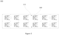
FIG 5 is a schematic diagram of the structure of another surface of the antenna oscillator module shown inFIG 4 . -
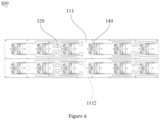
FIG 6 is a schematic diagram of the structure of one surface of the antenna oscillator module in another embodiment of the present invention. -
FIG 7 is a schematic diagram of the structure of the shield in the array antenna shown inFIG 1 . - In order to facilitate the understanding of the present application, the present application will be more fully described below with reference to the relevant accompanying drawings. Preferred embodiments of the present application are given in the accompanying drawings. However, the application can be implemented in many different forms and is not limited to the embodiments described herein. Rather, these embodiments are provided for the purpose of providing a more thorough and comprehensive understanding of the disclosure of the present application.
- It is noted that when an element is considered to be "fixed" to another element, it may be directly on the other element or there may also be a centered element. When an element is considered to be "attached" to another element, it can be directly attached to another element or there may also be a centered element. The terms "vertical", "horizontal", "left", "right" and similar expressions used herein are used for illustrative purposes only.
- Unless otherwise defined, all technical and scientific terms used herein have the same meaning as commonly understood by those skilled in the art of the application. The terms used herein in the specification of the present application are for the purpose of describing specific embodiments only and are not intended to limit the application. The term "and/or" as used herein includes any and all combinations of one or more of the relevant listed items.
- Referring to
FIGS. 1 ,2 , and3 , anarray antenna 10 in the preferred embodiment of the present application includes anantenna oscillator module 100, ashielding cavity 200, and adielectric filter module 300. - Referring to
FIGS. 4 and5 , theantenna oscillator module 100 includes adielectric substrate 110, a feednetwork line layer 120, and aradiation unit 130. Theantenna oscillator module 100 generally has multiple signal channels. For example, there are common 32 channels, 64 channels. Each signal channel contains at least oneradiation unit 130. As shown inFIGS. 2 and3 , in the embodiment, the number ofradiation unit 130 is 96, and each signal channel contains threeradiation units 130. Therefore, thearray antenna 10 is a 32-channel antenna. - The
dielectric substrate 110 is a one-piece structure, and its material can be plastic, resin, etc. Usually, thedielectric substrate 110 is molded in one piece by injection molding. The feednetwork line layer 120 is formed on the surface of thedielectric substrate 110. The feednetwork line layer 120 can integrate functional circuit such as divider circuit, filter circuit, etc., which can be used to feed theradiation unit 120, and is therefore equivalent to a conventional feed network. Specifically, the feednetwork line layer 120 can be formed on the surface of thedielectric substrate 110 by means of selective plating, LDS (laser direct forming technology) and other surface metal forming, and can be made of copper, silver and other good conductors. - The
radiation unit 130 is used for receiving and radiating electromagnetic wave signals outward, generally using a dual-polarized radiation unit. Theradiation unit 130 is provided on one side of thedielectric substrate 110, and is fed by the feednetwork line layer 120. Among them, the feednetwork line layer 120 can be directly fed to theradiation unit 130, can also be coupled to theradiation unit 130 for feed. Specifically, when the feednetwork line layer 120 is formed, a feedstructure line layer 140 may also be formed on thedielectric substrate 110 at the same time, and the feedstructure line layer 140 is supported by thedielectric substrate 110, which is equivalent to the traditional feed balun and feed column. - Each
array antenna 10 may include only oneantenna oscillator module 100, that is,multiple radiation units 130 are disposed on the samedielectric substrate 110; may also include a plurality ofantenna oscillator module 100, that is, the plurality ofradiation units 130 are disposed on differentdielectric substrate 110 and then joined together. As shown inFIGS. 2 and3 , specifically in this embodiment, eacharray antenna 10 includes 8antenna oscillator modules 100, and eachdielectric substrate 110 is provided with 12radiation units 130. 8dielectric substrate 110 are joined each other, thereby forming anantenna oscillator module 100 with 96radiation units 130. - The
radiation unit 130 can be in the form of metal oscillator structure, PCB oscillator structure, plastic metallization oscillator and metal laminate structure. Referring again toFIGS. 4 and5 , in one embodiment, thedielectric substrate 110 includes afeed substrate 111 and aradiation substrate 113 located on one side of thefeed substrate 111 and integrally formed with thefeed substrate 111. The feednetwork line layer 120 is formed on the surface of thefeed substrate 111, and the surface of theradiation substrate 113 is coated with a metal layer (not marked in the figure) to form theradiation unit 130. - Specifically, the metal layer can also be formed by means of selective plating, LDS (laser direct forming technology) and other surface metal forming way. The
radiation substrate 113 supports the metal layer, and forms theradiation unit 130 together with the metal layer together. At this time, theradiation unit 130 and thedielectric substrate 110 constitute a one-piece structure. In other words, the traditional radiation unit and feed network can be integrated on thedielectric substrate 110, so the structure of theantenna oscillator module 100 can be simplified, and its volume and weight can be significantly reduced. - The
radiation substrate 113 can be a hollow column-shaped projection formed by a local recess from thefeed substrate 111. The metal layer forming theradiation unit 130 is attached to the outer surface of the column-shaped projection. Specifically, the hollow column-shaped projection may be cube-shaped or cylindrical, i.e., its cross-section is rectangular or circular. Wherein, the feedstructure line layer 140 may be supported by the inner wall of the column-shaped projection and extend along the inner wall toward theradiation unit 130. By making a local recess in thefeed substrate 111 to form the support structure of theradiation unit 130, the structure of thedielectric substrate 110 can be made more reasonable and the yield rate of injection molding is better. - Further, the feed
network line layer 120 can be located either on the same or different side of thedielectric substrate 110 as theradiation unit 130. As shown inFIGS. 4 and5 , in one embodiment, the feednetwork line layer 120 is located on the surface of thefeed substrate 111 facing away from theradiation unit 130. Meanwhile, the feednetwork line layer 120 may be integrally formed with the feedstructure line layer 140. - As shown in
FIG 6 , in another embodiment, the feednetwork line layer 120 is disposed on a surface of thefeed substrate 111 toward theradiation unit 130. Meanwhile, the feednetwork line layer 120 may be electrically connected to the feedstructure line layer 140 by opening a metallized perforation. - Referring again to
FIGS. 1 to 3 , ashielding cavity 200 is formed on one side of thedielectric substrate 110 facing away from theradiation unit 130. The shieldingcavity 200 may be a closed cavity structure mounted on one side of thedielectric substrate 110 by welding, screwing, etc.; theshielding cavity 200 may also be a cavity structure with a shielding function obtained by forming integrally with thedielectric substrate 110 and metallizing the surface; theshielding cavity 200 may also be a closed cavity structure formed by a semi-closed structure cooperating with thedielectric substrate 110. The shieldingcavity 200 can play the role of electrostatic shielding, equivalent to the metal shielding cavity of traditional dielectric filter. - In this embodiment, the
array antenna 10 also includes areflective plate 500, thereflective plate 500 is affixed to the side of thedielectric substrate 110 facing away from theradiation unit 130. - Specifically, the
reflective plate 500 is generally a metal reflective plate, which can reflect the electromagnetic wave signal several times, thus enhancing the efficiency of signal transmitting and receiving of theradiation unit 130. The surface profile of thereflective plate 500 is generally substantially the same as the surface profile of thedielectric substrate 110, and the surfaces of both are disposed opposite each other. Thereflective plate 500 can be screwed, welded and other ways to achieve installation with thedielectric substrate 110. - Referring again to
FIG 6 , in one embodiment, a raisedrib 1112 is formed on the surface of thedielectric substrate 110 facing thereflective plate 500, and therib 1112 abuts thereflective plate 500. - Specifically, the
rib 1112 is formed on thefeed substrate 111. Therib 1112 may be distributed in a circular pattern on the surface of thefeed substrate 111 or may extend in a straight line on the surface of thefeed substrate 111. On the one hand, therib 1112 may serve to strengthen the mechanical strength of thefeed substrate 111. On the other hand, therib 1112 may support thereflective plate 500 so as to maintain a stable gap between thereflective plate 500 and thefeed substrate 111. When the feednetwork line layer 120 is located on the side of thefeed substrate 111 facing away from theradiation unit 130, it can ensure the isolation of the feednetwork line layer 120 from thereflective plate 500. - Further, in this embodiment, the
array antenna 10 also includes ashield 600 with an opening on one side, and theshield 600 is covered on the surface of thereflector plate 500 facing away from theantenna oscillator module 100 and cooperates with thereflective plate 500 to form theshielding cavity 200. - Specifically, the
shield 600 can be in the shape of a cube, a hemisphere or a semi-cylindrical shape, etc., with an opening on one side. Theshield 600 can be formed directly from the metal material; or it can be formed by the dielectric material first, and then the surface of the dielectric material can be metallized. Theshield 600 is generally fastened to thereflective plate 500 by screws. At this time, thereflective plate 500 acts as a sidewall of theshielding cavity 200. Therefore, theshield 600 can also omit a sidewall compared with the conventional metal shielding cavity, so the weight can be further reduced. - Referring together to
FIG 7 , specifically in this embodiment, the end surface of the opening of theshield 600 is covered with aconductive adhesive 610. Theconductive adhesive 610 can make good contact with the edge of the opening of theshield 600, thus ensuring the shielding effect of theshielding cavity 200. - The
dielectric filter module 300 is equivalent to the filter body structure after the traditional dielectric filter omitting the metal shielding cavity. There are multipledielectric filter modules 300, and the output of eachdielectric filter module 300 is electrically connected to the feednetwork line layer 120. Thedielectric filter module 300 is used to filter the electromagnetic wave signal received or radiated by eachradiation unit 130. Thus, thedielectric filter modules 300 correspond to the number of signal channels of thearray antenna 10. For example, if thearray antenna 10 shown inFIG 1 has 32 signal channels, the number ofdielectric filter modules 300 is 32. - Further, a plurality of
dielectric filter modules 300 are provided in theshielding cavity 200, and each shieldingcavity 200 houses at least twodielectric filter modules 300. Depending on the size of the antenna, one ormore shielding cavities 200 may be included in eacharray antenna 10. For example, thearray antenna 10 shown inFIG 1 includes two shieldingcavities 200, each shieldingcavity 200 contains 16filter modules 300. - In other words, one
shielding cavity 200 can provide electrostatic shielding effect on a plurality ofdielectric filter modules 300, so the number of shieldingcavities 200 can be much less than the number ofdielectric filter modules 300. In conventional technology, for 32-channel antenna, 32 filters need to be installed, and each filter has a metal shielding cavity. In this scheme, for 32-channel array antenna 10, only two shieldingcavities 200 need to be installed. Therefore, compared with the traditional way, thearray antenna 100 can omit more metal shielding cavities, thus simplifying the installation operation and reducing the weight. - Referring again to
FIG 7 , specifically in this embodiment, the inner wall of theshield 600 is provided with aconductive foam 620 that abuts thedielectric filter module 300. - The
conductive foam 620 extends along the length of theshield 600, thus covering all thedielectric filter modules 300 in theshielding cavity 200. Thus, theconductive foam 620 connects theshield 600 to the surface of eachdielectric filter module 300, so that eachdielectric filter module 300 is well grounded, thus suppressing high frequency clutter caused by surface current radiation. - In this embodiment, the
array antenna 10 also includes acircuit board 400, a plurality ofdielectric filter modules 300 are integrated in thecircuit board 400, and the outputs of the plurality ofdielectric filter modules 300 are electrically connected to the feednetwork line layer 120 through thecircuit board 400. - The plurality of
dielectric filter modules 300 can be positioned and soldered on thecircuit board 400 first, and then thecircuit board 400 integrated with thedielectric filter modules 300 as a whole is connected to the feednetwork line layer 120. Therefore, it is only necessary to align thecircuit board 400 as a whole with the feed network line layer 12, instead of repeating the positioning of eachdielectric filter module 300, so it can make the assembly more convenient. Among them, the number ofcircuit boards 400 can be the same as the number of shieldingcavities 200, or alldielectric filter modules 300 can be integrated on thesame circuit board 400. - The
array antenna 10 shown inFIGS 1 to 3 has 2circuit boards 400, and eachcircuit board 400 has 16dielectric filter modules 300 integrated thereon. The shieldingcavity 200 holds thecorresponding circuit board 400 on thereflective plate 500. - Further, in this embodiment, the
circuit board 400 is provided with aRF connector 410 and afeed pin 420 on opposite sides, and theRF connector 410 andfeed pin 420 correspond to the plurality ofdielectric filter modules 300 one by one. The feednetwork line layer 120 is formed with feed holes (not shown), and thefeed pin 420 is inserted in the feed hole to electrically connect the plurality ofdielectric filter modules 300 to the feednetwork line layer 120. - Specifically, the
RF connector 410 and thefeed pin 420 are connected to the input and output of the correspondingdielectric filter module 300, respectively. The feed hole on the feednetwork line layer 120 may be metallized via hole that is electrically conductive. Moreover, the position of the feed hole corresponds to the position of thefeed pin 420. Thereflective plate 500 is provided with avoidance hole for avoidance of the feed pin 420 (not shown). Upon assembling, thefeed pin 420 is inserted into the corresponding feed hole, the positioning and installation of theboard 400 is quickly realized, so the assembly is more convenient. - The
RF connector 410 can be used with the plug interface of the coaxial feed to facilitate the connection between thedielectric filter module 300 and the signal transceiver device of the base station. Among them, theRF connector 410 generally protrudes to the outside of theshielding cavity 200, and the side wall of theshielding cavity 200 is opened with a throughhole 210 forRF connector 410 to pass through. - The
array antenna 10 described above, the feednetwork line layer 120 may be formed on the surface of thedielectric substrate 110 by means of coating, etc. Therefore, it is equivalent to integrating the feed network andradiation unit 130 of the conventional antenna on thedielectric substrate 110. When assembling, there is no need to weld and screw the feed network and other operations, which helps to simplify the structure. Further, the shieldingcavity 200 provides shielding to thedielectric filter module 300 inside, so the plurality ofdielectric filter modules 300 with the shieldingcavity 200 can be functionally equivalent to the traditional multiple dielectric filters. Moreover, each shieldingcavity 200 houses at least twodielectric filter modules 300, so the number of shieldingcavities 200 can be much less than the number ofdielectric filter modules 300. Compared with the traditional way of directly mounting dielectric filters, a larger number of metal shielding cavities can be omitted. As a result, theabove array antenna 10 can achieve light weight. - Each technical feature of the above described embodiment can be combined in any way, for the sake of concise description, not all possible combinations of each technical feature of the above described embodiment are described. However, as long as the combination of these technical features are not contradictory, it should be considered as the scope of this description.
- The above described embodiments express only several embodiments of the present application with more specific and detailed descriptions, but they are not to be construed as a limitation of the scope of the application. It should be noted that for a person of ordinary skilled in the art, a number of deformations and improvements can be made without departing from the scope of the present application. Therefore, the scope of protection of the present application shall be subject to the attached claims.
Claims (7)
- An array antenna (10), comprising:an antenna oscillator module (100) including a dielectric substrate (110), a feed network line layer (120) formed on a surface of the dielectric substrate (110) and a plurality of radiation units (130) disposed on one side of the dielectric substrate (110) and fed by the feed network line layer (120);a shielding cavity (200) formed on one side of the dielectric substrate (110) facing away from the radiation unit (130); anda plurality of dielectric filter modules (300) disposed within the shielding cavity (200), and each shielding cavity (200) housing at least two of the dielectric filter modules (300), an output of each of the dielectric filter modules (300) being electrically connected to the feed network line layer (120);a reflective plate (500) affixed to one side of the dielectric substrate (110) facing away from the radiation unit (130);a shield (600) with an opening on one side, wherein, the shield (600) is provided on a surface of the reflective plate (500) facing away from the antenna oscillator module (100) and cooperating with the reflective plate (500) to form the shielding cavity (200);wherein, an inner wall of the shield (600) is provided with a conductive foam (620) abutting against the dielectric filter module (300).
- The array antenna (10) according to claim 1, wherein, the dielectric substrate (110) comprises a feed substrate (111) and a radiation substrate (113) disposed on one side of the feed substrate (111) and integrally formed with the feed substrate (111), wherein, the feed network line layer (120) is formed on a surface of the feed substrate (111), the radiation substrate (113) is coated with a metal layer on a surface to form the radiation unit (130).
- The array antenna (10) according to claim 2, wherein, the feed network line layer (120) is disposed on a surface of the feed substrate (111) facing away from the radiation unit (130),
or, the feed network line layer (120) is disposed on a surface of the feed substrate (111) facing the radiation unit (130). - The array antenna (10) according to claim 1, further comprising: a circuit board (400), wherein, the plurality of dielectric filter modules (300) are integrated in the circuit board (400), and the outputs of the plurality of dielectric filter modules (300) are electrically connected to the feed network line layer (120) through the circuit board (400).
- The array antenna (10) according to claim 4, wherein, the circuit board (400) is provided with RF connectors (410) and feed pins (420) corresponding to the plurality of dielectric filter modules (300) one by one on opposite sides, wherein, the feed network line layer (120) is formed with feed holes, the feed pins (420) are inserted in the feed holes to electrically connect the plurality of dielectric filter modules (300) to the feed network line layer (120).
- The array antenna (10) according to claim 1, wherein, the dielectric substrate (110) is formed with raised ribs (1112) on a surface toward the reflective plate (500), and the ribs are abutted against the reflective plate (500).
- The array antenna (10) according to claim 1, wherein, the shield (600) is coated with a conductive adhesive (610) on an end surface of the opening.
Applications Claiming Priority (2)
| Application Number | Priority Date | Filing Date | Title |
|---|---|---|---|
| CN201911417972.XA CN111063997B (en) | 2019-12-31 | 2019-12-31 | Array Antenna |
| PCT/CN2020/110270 WO2021135266A1 (en) | 2019-12-31 | 2020-08-20 | Array antenna |
Publications (4)
| Publication Number | Publication Date |
|---|---|
| EP4087057A1 EP4087057A1 (en) | 2022-11-09 |
| EP4087057A4 EP4087057A4 (en) | 2023-01-18 |
| EP4087057C0 EP4087057C0 (en) | 2025-07-02 |
| EP4087057B1 true EP4087057B1 (en) | 2025-07-02 |
Family
ID=70305874
Family Applications (1)
| Application Number | Title | Priority Date | Filing Date |
|---|---|---|---|
| EP20909313.7A Active EP4087057B1 (en) | 2019-12-31 | 2020-08-20 | Array antenna |
Country Status (3)
| Country | Link |
|---|---|
| EP (1) | EP4087057B1 (en) |
| CN (1) | CN111063997B (en) |
| WO (1) | WO2021135266A1 (en) |
Families Citing this family (8)
| Publication number | Priority date | Publication date | Assignee | Title |
|---|---|---|---|---|
| CN112490646B (en) | 2019-09-12 | 2023-12-15 | 华为技术有限公司 | An antenna and an antenna processing method |
| CN111063997B (en) * | 2019-12-31 | 2024-12-20 | 京信通信技术(广州)有限公司 | Array Antenna |
| CN111585007B (en) * | 2020-05-08 | 2022-04-15 | 武汉虹信科技发展有限责任公司 | Highly integrated MIMO antenna |
| EP4160817A4 (en) * | 2020-05-26 | 2024-06-12 | KMW Inc. | ANTENNA DEVICE |
| CN111668605B (en) * | 2020-07-02 | 2021-07-09 | 中信科移动通信技术股份有限公司 | Electrically-controlled antenna used along high-speed rail |
| CN116897471A (en) | 2021-12-31 | 2023-10-17 | 京东方科技集团股份有限公司 | Transparent vibrator unit, transparent antenna and antenna system |
| CN116454605B (en) * | 2023-04-03 | 2025-12-30 | 中天通信技术有限公司 | Wall-mounted antenna |
| CN119234353B (en) | 2023-04-28 | 2026-01-16 | 京东方科技集团股份有限公司 | Antenna and electronic equipment |
Family Cites Families (9)
| Publication number | Priority date | Publication date | Assignee | Title |
|---|---|---|---|---|
| CN1893179A (en) * | 2005-07-08 | 2007-01-10 | 福讯通讯股份有限公司 | Antennas for Handheld Devices |
| CN107706544B (en) * | 2017-09-07 | 2021-01-26 | 广东通宇通讯股份有限公司 | Base station antenna and antenna array module thereof |
| CN109616759B (en) * | 2018-12-06 | 2020-08-25 | 西南电子技术研究所(中国电子科技集团公司第十研究所) | Full-duplex active phased array filtering antenna array surface |
| CN109713432A (en) * | 2019-01-14 | 2019-05-03 | 深圳市信维通信股份有限公司 | 5G mimo antenna system and handheld device |
| CN110011072B (en) * | 2019-02-22 | 2024-02-20 | 广东通宇通讯股份有限公司 | Integrated Massive MIMO antenna |
| CN210723355U (en) * | 2019-04-30 | 2020-06-09 | 深圳市大富科技股份有限公司 | Base station antenna and active antenna unit for base station |
| CN110323556A (en) * | 2019-05-08 | 2019-10-11 | 深圳市大富科技股份有限公司 | A kind of active antenna element and antenna element for base station |
| CN211126065U (en) * | 2019-12-31 | 2020-07-28 | 京信通信技术(广州)有限公司 | Array antenna |
| CN111063997B (en) * | 2019-12-31 | 2024-12-20 | 京信通信技术(广州)有限公司 | Array Antenna |
-
2019
- 2019-12-31 CN CN201911417972.XA patent/CN111063997B/en active Active
-
2020
- 2020-08-20 EP EP20909313.7A patent/EP4087057B1/en active Active
- 2020-08-20 WO PCT/CN2020/110270 patent/WO2021135266A1/en not_active Ceased
Also Published As
| Publication number | Publication date |
|---|---|
| WO2021135266A1 (en) | 2021-07-08 |
| EP4087057C0 (en) | 2025-07-02 |
| CN111063997A (en) | 2020-04-24 |
| CN111063997B (en) | 2024-12-20 |
| EP4087057A1 (en) | 2022-11-09 |
| EP4087057A4 (en) | 2023-01-18 |
Similar Documents
| Publication | Publication Date | Title |
|---|---|---|
| EP4087057A1 (en) | Array antenna | |
| CN111129737B (en) | Antenna unit and array antenna | |
| JP7246490B2 (en) | Antenna structure and high-frequency multi-band wireless communication terminal | |
| US7483728B2 (en) | Portable communication unit and internal antenna used for same | |
| KR102168317B1 (en) | Mobile terminal and antenna radiation method of mobile terminal | |
| US20230163441A1 (en) | Antenna device | |
| CN110574228B (en) | Antenna for use in frame of display panel | |
| KR20170083949A (en) | Wireless communication device with leaky wave phased array antenna | |
| JP2018117349A (en) | MIMO antenna apparatus and mobile communication apparatus | |
| CN109494489B (en) | Filtering integrated base station antenna | |
| WO2022042239A1 (en) | Button, card tray, camera decoration accessory, and mobile terminal | |
| CN210692758U (en) | Antenna with integrated filter | |
| CN111987410A (en) | Modular AFU structure | |
| CN110911837B (en) | Antenna with integrated filter | |
| WO2020259001A1 (en) | Filter antenna and base station device | |
| US6943738B1 (en) | Compact multiband inverted-F antenna | |
| CN117353051A (en) | Electronic equipment | |
| CN211126054U (en) | Antenna unit and array antenna | |
| US5276457A (en) | Integrated antenna-converter system in a unitary package | |
| CN212412206U (en) | Feed network, antenna system and base station | |
| CN114171912A (en) | UWB patch antenna, antenna structure, housing assembly, and electronic device | |
| CN210957014U (en) | Phase-shift feeding device, antenna unit and array antenna | |
| US12603431B2 (en) | Antenna element and antenna array | |
| KR102528198B1 (en) | Antenna apparatus | |
| CN211126065U (en) | Array antenna |
Legal Events
| Date | Code | Title | Description |
|---|---|---|---|
| STAA | Information on the status of an ep patent application or granted ep patent |
Free format text: STATUS: THE INTERNATIONAL PUBLICATION HAS BEEN MADE |
|
| PUAI | Public reference made under article 153(3) epc to a published international application that has entered the european phase |
Free format text: ORIGINAL CODE: 0009012 |
|
| STAA | Information on the status of an ep patent application or granted ep patent |
Free format text: STATUS: REQUEST FOR EXAMINATION WAS MADE |
|
| 17P | Request for examination filed |
Effective date: 20220711 |
|
| AK | Designated contracting states |
Kind code of ref document: A1 Designated state(s): AL AT BE BG CH CY CZ DE DK EE ES FI FR GB GR HR HU IE IS IT LI LT LU LV MC MK MT NL NO PL PT RO RS SE SI SK SM TR |
|
| REG | Reference to a national code |
Ref country code: DE Ref legal event code: R079 Free format text: PREVIOUS MAIN CLASS: H01Q0001380000 Ipc: H01Q0021000000 Ref country code: DE Ref legal event code: R079 Ref document number: 602020054014 Country of ref document: DE Free format text: PREVIOUS MAIN CLASS: H01Q0001380000 Ipc: H01Q0021000000 |
|
| A4 | Supplementary search report drawn up and despatched |
Effective date: 20221216 |
|
| RIC1 | Information provided on ipc code assigned before grant |
Ipc: H01Q 21/06 20060101ALI20221212BHEP Ipc: H01Q 1/24 20060101ALI20221212BHEP Ipc: H01Q 1/52 20060101ALI20221212BHEP Ipc: H01Q 21/00 20060101AFI20221212BHEP |
|
| DAV | Request for validation of the european patent (deleted) | ||
| DAX | Request for extension of the european patent (deleted) | ||
| P01 | Opt-out of the competence of the unified patent court (upc) registered |
Effective date: 20230517 |
|
| REG | Reference to a national code |
Ref country code: DE Ref legal event code: R079 Free format text: PREVIOUS MAIN CLASS: H01Q0021000000 Ipc: H01Q0001240000 Ref country code: DE Ref legal event code: R079 Ref document number: 602020054014 Country of ref document: DE Free format text: PREVIOUS MAIN CLASS: H01Q0021000000 Ipc: H01Q0001240000 |
|
| RIC1 | Information provided on ipc code assigned before grant |
Ipc: H01Q 21/00 20060101ALN20250114BHEP Ipc: H01Q 21/06 20060101ALI20250114BHEP Ipc: H01Q 1/52 20060101ALI20250114BHEP Ipc: H01Q 1/24 20060101AFI20250114BHEP |
|
| RIC1 | Information provided on ipc code assigned before grant |
Ipc: H01Q 21/00 20060101ALN20250127BHEP Ipc: H01Q 21/06 20060101ALI20250127BHEP Ipc: H01Q 1/52 20060101ALI20250127BHEP Ipc: H01Q 1/24 20060101AFI20250127BHEP |
|
| GRAP | Despatch of communication of intention to grant a patent |
Free format text: ORIGINAL CODE: EPIDOSNIGR1 |
|
| STAA | Information on the status of an ep patent application or granted ep patent |
Free format text: STATUS: GRANT OF PATENT IS INTENDED |
|
| INTG | Intention to grant announced |
Effective date: 20250310 |
|
| GRAS | Grant fee paid |
Free format text: ORIGINAL CODE: EPIDOSNIGR3 |
|
| GRAA | (expected) grant |
Free format text: ORIGINAL CODE: 0009210 |
|
| STAA | Information on the status of an ep patent application or granted ep patent |
Free format text: STATUS: THE PATENT HAS BEEN GRANTED |
|
| AK | Designated contracting states |
Kind code of ref document: B1 Designated state(s): AL AT BE BG CH CY CZ DE DK EE ES FI FR GB GR HR HU IE IS IT LI LT LU LV MC MK MT NL NO PL PT RO RS SE SI SK SM TR |
|
| REG | Reference to a national code |
Ref country code: GB Ref legal event code: FG4D |
|
| REG | Reference to a national code |
Ref country code: CH Ref legal event code: EP |
|
| REG | Reference to a national code |
Ref country code: DE Ref legal event code: R096 Ref document number: 602020054014 Country of ref document: DE |
|
| REG | Reference to a national code |
Ref country code: IE Ref legal event code: FG4D |
|
| U01 | Request for unitary effect filed |
Effective date: 20250711 |
|
| U07 | Unitary effect registered |
Designated state(s): AT BE BG DE DK EE FI FR IT LT LU LV MT NL PT RO SE SI Effective date: 20250717 |
|
| U20 | Renewal fee for the european patent with unitary effect paid |
Year of fee payment: 6 Effective date: 20250924 |
|
| PG25 | Lapsed in a contracting state [announced via postgrant information from national office to epo] |
Ref country code: IS Free format text: LAPSE BECAUSE OF FAILURE TO SUBMIT A TRANSLATION OF THE DESCRIPTION OR TO PAY THE FEE WITHIN THE PRESCRIBED TIME-LIMIT Effective date: 20251102 |
|
| PG25 | Lapsed in a contracting state [announced via postgrant information from national office to epo] |
Ref country code: NO Free format text: LAPSE BECAUSE OF FAILURE TO SUBMIT A TRANSLATION OF THE DESCRIPTION OR TO PAY THE FEE WITHIN THE PRESCRIBED TIME-LIMIT Effective date: 20251002 |
|
| PG25 | Lapsed in a contracting state [announced via postgrant information from national office to epo] |
Ref country code: HR Free format text: LAPSE BECAUSE OF FAILURE TO SUBMIT A TRANSLATION OF THE DESCRIPTION OR TO PAY THE FEE WITHIN THE PRESCRIBED TIME-LIMIT Effective date: 20250702 |
|
| PG25 | Lapsed in a contracting state [announced via postgrant information from national office to epo] |
Ref country code: GR Free format text: LAPSE BECAUSE OF FAILURE TO SUBMIT A TRANSLATION OF THE DESCRIPTION OR TO PAY THE FEE WITHIN THE PRESCRIBED TIME-LIMIT Effective date: 20251003 |
|
| PG25 | Lapsed in a contracting state [announced via postgrant information from national office to epo] |
Ref country code: CZ Free format text: LAPSE BECAUSE OF FAILURE TO SUBMIT A TRANSLATION OF THE DESCRIPTION OR TO PAY THE FEE WITHIN THE PRESCRIBED TIME-LIMIT Effective date: 20250702 |
|
| PG25 | Lapsed in a contracting state [announced via postgrant information from national office to epo] |
Ref country code: PL Free format text: LAPSE BECAUSE OF FAILURE TO SUBMIT A TRANSLATION OF THE DESCRIPTION OR TO PAY THE FEE WITHIN THE PRESCRIBED TIME-LIMIT Effective date: 20250702 |
|
| PG25 | Lapsed in a contracting state [announced via postgrant information from national office to epo] |
Ref country code: RS Free format text: LAPSE BECAUSE OF FAILURE TO SUBMIT A TRANSLATION OF THE DESCRIPTION OR TO PAY THE FEE WITHIN THE PRESCRIBED TIME-LIMIT Effective date: 20251002 |
|
| PG25 | Lapsed in a contracting state [announced via postgrant information from national office to epo] |
Ref country code: ES Free format text: LAPSE BECAUSE OF FAILURE TO SUBMIT A TRANSLATION OF THE DESCRIPTION OR TO PAY THE FEE WITHIN THE PRESCRIBED TIME-LIMIT Effective date: 20250702 |
|
| REG | Reference to a national code |
Ref country code: CH Ref legal event code: H13 Free format text: ST27 STATUS EVENT CODE: U-0-0-H10-H13 (AS PROVIDED BY THE NATIONAL OFFICE) Effective date: 20260324 |
|
| PG25 | Lapsed in a contracting state [announced via postgrant information from national office to epo] |
Ref country code: SM Free format text: LAPSE BECAUSE OF FAILURE TO SUBMIT A TRANSLATION OF THE DESCRIPTION OR TO PAY THE FEE WITHIN THE PRESCRIBED TIME-LIMIT Effective date: 20250702 |
|
| PG25 | Lapsed in a contracting state [announced via postgrant information from national office to epo] |
Ref country code: CH Free format text: LAPSE BECAUSE OF NON-PAYMENT OF DUE FEES Effective date: 20250831 |
|
| PG25 | Lapsed in a contracting state [announced via postgrant information from national office to epo] |
Ref country code: SK Free format text: LAPSE BECAUSE OF FAILURE TO SUBMIT A TRANSLATION OF THE DESCRIPTION OR TO PAY THE FEE WITHIN THE PRESCRIBED TIME-LIMIT Effective date: 20250702 |
|
| PLBE | No opposition filed within time limit |
Free format text: ORIGINAL CODE: 0009261 |
|
| STAA | Information on the status of an ep patent application or granted ep patent |
Free format text: STATUS: NO OPPOSITION FILED WITHIN TIME LIMIT |