EP4086939A1 - A layered structure including an intermediate bixbyite oxide layer - Google Patents
A layered structure including an intermediate bixbyite oxide layer Download PDFInfo
- Publication number
- EP4086939A1 EP4086939A1 EP22169996.0A EP22169996A EP4086939A1 EP 4086939 A1 EP4086939 A1 EP 4086939A1 EP 22169996 A EP22169996 A EP 22169996A EP 4086939 A1 EP4086939 A1 EP 4086939A1
- Authority
- EP
- European Patent Office
- Prior art keywords
- bixbyite
- layer
- layered structure
- metal
- crystalline
- Prior art date
- Legal status (The legal status is an assumption and is not a legal conclusion. Google has not performed a legal analysis and makes no representation as to the accuracy of the status listed.)
- Pending
Links
Images



Classifications
-
- H—ELECTRICITY
- H10—SEMICONDUCTOR DEVICES; ELECTRIC SOLID-STATE DEVICES NOT OTHERWISE PROVIDED FOR
- H10D—INORGANIC ELECTRIC SEMICONDUCTOR DEVICES
- H10D62/00—Semiconductor bodies, or regions thereof, of devices having potential barriers
- H10D62/80—Semiconductor bodies, or regions thereof, of devices having potential barriers characterised by the materials
- H10D62/85—Semiconductor bodies, or regions thereof, of devices having potential barriers characterised by the materials being Group III-V materials, e.g. GaAs
- H10D62/8503—Nitride Group III-V materials, e.g. AlN or GaN
-
- H—ELECTRICITY
- H10—SEMICONDUCTOR DEVICES; ELECTRIC SOLID-STATE DEVICES NOT OTHERWISE PROVIDED FOR
- H10P—GENERIC PROCESSES OR APPARATUS FOR THE MANUFACTURE OR TREATMENT OF DEVICES COVERED BY CLASS H10
- H10P14/00—Formation of materials, e.g. in the shape of layers or pillars
- H10P14/20—Formation of materials, e.g. in the shape of layers or pillars of semiconductor materials
- H10P14/32—Formation of materials, e.g. in the shape of layers or pillars of semiconductor materials characterised by intermediate layers between substrates and deposited layers
- H10P14/3242—Structure
- H10P14/3244—Layer structure
- H10P14/3248—Layer structure consisting of two layers
-
- C—CHEMISTRY; METALLURGY
- C30—CRYSTAL GROWTH
- C30B—SINGLE-CRYSTAL GROWTH; UNIDIRECTIONAL SOLIDIFICATION OF EUTECTIC MATERIAL OR UNIDIRECTIONAL DEMIXING OF EUTECTOID MATERIAL; REFINING BY ZONE-MELTING OF MATERIAL; PRODUCTION OF A HOMOGENEOUS POLYCRYSTALLINE MATERIAL WITH DEFINED STRUCTURE; SINGLE CRYSTALS OR HOMOGENEOUS POLYCRYSTALLINE MATERIAL WITH DEFINED STRUCTURE; AFTER-TREATMENT OF SINGLE CRYSTALS OR A HOMOGENEOUS POLYCRYSTALLINE MATERIAL WITH DEFINED STRUCTURE; APPARATUS THEREFOR
- C30B23/00—Single-crystal growth by condensing evaporated or sublimed materials
- C30B23/02—Epitaxial-layer growth
-
- C—CHEMISTRY; METALLURGY
- C30—CRYSTAL GROWTH
- C30B—SINGLE-CRYSTAL GROWTH; UNIDIRECTIONAL SOLIDIFICATION OF EUTECTIC MATERIAL OR UNIDIRECTIONAL DEMIXING OF EUTECTOID MATERIAL; REFINING BY ZONE-MELTING OF MATERIAL; PRODUCTION OF A HOMOGENEOUS POLYCRYSTALLINE MATERIAL WITH DEFINED STRUCTURE; SINGLE CRYSTALS OR HOMOGENEOUS POLYCRYSTALLINE MATERIAL WITH DEFINED STRUCTURE; AFTER-TREATMENT OF SINGLE CRYSTALS OR A HOMOGENEOUS POLYCRYSTALLINE MATERIAL WITH DEFINED STRUCTURE; APPARATUS THEREFOR
- C30B23/00—Single-crystal growth by condensing evaporated or sublimed materials
- C30B23/02—Epitaxial-layer growth
- C30B23/025—Epitaxial-layer growth characterised by the substrate
-
- C—CHEMISTRY; METALLURGY
- C30—CRYSTAL GROWTH
- C30B—SINGLE-CRYSTAL GROWTH; UNIDIRECTIONAL SOLIDIFICATION OF EUTECTIC MATERIAL OR UNIDIRECTIONAL DEMIXING OF EUTECTOID MATERIAL; REFINING BY ZONE-MELTING OF MATERIAL; PRODUCTION OF A HOMOGENEOUS POLYCRYSTALLINE MATERIAL WITH DEFINED STRUCTURE; SINGLE CRYSTALS OR HOMOGENEOUS POLYCRYSTALLINE MATERIAL WITH DEFINED STRUCTURE; AFTER-TREATMENT OF SINGLE CRYSTALS OR A HOMOGENEOUS POLYCRYSTALLINE MATERIAL WITH DEFINED STRUCTURE; APPARATUS THEREFOR
- C30B29/00—Single crystals or homogeneous polycrystalline material with defined structure characterised by the material or by their shape
- C30B29/02—Elements
-
- C—CHEMISTRY; METALLURGY
- C30—CRYSTAL GROWTH
- C30B—SINGLE-CRYSTAL GROWTH; UNIDIRECTIONAL SOLIDIFICATION OF EUTECTIC MATERIAL OR UNIDIRECTIONAL DEMIXING OF EUTECTOID MATERIAL; REFINING BY ZONE-MELTING OF MATERIAL; PRODUCTION OF A HOMOGENEOUS POLYCRYSTALLINE MATERIAL WITH DEFINED STRUCTURE; SINGLE CRYSTALS OR HOMOGENEOUS POLYCRYSTALLINE MATERIAL WITH DEFINED STRUCTURE; AFTER-TREATMENT OF SINGLE CRYSTALS OR A HOMOGENEOUS POLYCRYSTALLINE MATERIAL WITH DEFINED STRUCTURE; APPARATUS THEREFOR
- C30B29/00—Single crystals or homogeneous polycrystalline material with defined structure characterised by the material or by their shape
- C30B29/10—Inorganic compounds or compositions
- C30B29/16—Oxides
-
- C—CHEMISTRY; METALLURGY
- C30—CRYSTAL GROWTH
- C30B—SINGLE-CRYSTAL GROWTH; UNIDIRECTIONAL SOLIDIFICATION OF EUTECTIC MATERIAL OR UNIDIRECTIONAL DEMIXING OF EUTECTOID MATERIAL; REFINING BY ZONE-MELTING OF MATERIAL; PRODUCTION OF A HOMOGENEOUS POLYCRYSTALLINE MATERIAL WITH DEFINED STRUCTURE; SINGLE CRYSTALS OR HOMOGENEOUS POLYCRYSTALLINE MATERIAL WITH DEFINED STRUCTURE; AFTER-TREATMENT OF SINGLE CRYSTALS OR A HOMOGENEOUS POLYCRYSTALLINE MATERIAL WITH DEFINED STRUCTURE; APPARATUS THEREFOR
- C30B29/00—Single crystals or homogeneous polycrystalline material with defined structure characterised by the material or by their shape
- C30B29/10—Inorganic compounds or compositions
- C30B29/40—AIIIBV compounds wherein A is B, Al, Ga, In or Tl and B is N, P, As, Sb or Bi
-
- C—CHEMISTRY; METALLURGY
- C30—CRYSTAL GROWTH
- C30B—SINGLE-CRYSTAL GROWTH; UNIDIRECTIONAL SOLIDIFICATION OF EUTECTIC MATERIAL OR UNIDIRECTIONAL DEMIXING OF EUTECTOID MATERIAL; REFINING BY ZONE-MELTING OF MATERIAL; PRODUCTION OF A HOMOGENEOUS POLYCRYSTALLINE MATERIAL WITH DEFINED STRUCTURE; SINGLE CRYSTALS OR HOMOGENEOUS POLYCRYSTALLINE MATERIAL WITH DEFINED STRUCTURE; AFTER-TREATMENT OF SINGLE CRYSTALS OR A HOMOGENEOUS POLYCRYSTALLINE MATERIAL WITH DEFINED STRUCTURE; APPARATUS THEREFOR
- C30B29/00—Single crystals or homogeneous polycrystalline material with defined structure characterised by the material or by their shape
- C30B29/10—Inorganic compounds or compositions
- C30B29/40—AIIIBV compounds wherein A is B, Al, Ga, In or Tl and B is N, P, As, Sb or Bi
- C30B29/403—AIII-nitrides
-
- C—CHEMISTRY; METALLURGY
- C30—CRYSTAL GROWTH
- C30B—SINGLE-CRYSTAL GROWTH; UNIDIRECTIONAL SOLIDIFICATION OF EUTECTIC MATERIAL OR UNIDIRECTIONAL DEMIXING OF EUTECTOID MATERIAL; REFINING BY ZONE-MELTING OF MATERIAL; PRODUCTION OF A HOMOGENEOUS POLYCRYSTALLINE MATERIAL WITH DEFINED STRUCTURE; SINGLE CRYSTALS OR HOMOGENEOUS POLYCRYSTALLINE MATERIAL WITH DEFINED STRUCTURE; AFTER-TREATMENT OF SINGLE CRYSTALS OR A HOMOGENEOUS POLYCRYSTALLINE MATERIAL WITH DEFINED STRUCTURE; APPARATUS THEREFOR
- C30B29/00—Single crystals or homogeneous polycrystalline material with defined structure characterised by the material or by their shape
- C30B29/10—Inorganic compounds or compositions
- C30B29/40—AIIIBV compounds wherein A is B, Al, Ga, In or Tl and B is N, P, As, Sb or Bi
- C30B29/403—AIII-nitrides
- C30B29/406—Gallium nitride
-
- C—CHEMISTRY; METALLURGY
- C30—CRYSTAL GROWTH
- C30B—SINGLE-CRYSTAL GROWTH; UNIDIRECTIONAL SOLIDIFICATION OF EUTECTIC MATERIAL OR UNIDIRECTIONAL DEMIXING OF EUTECTOID MATERIAL; REFINING BY ZONE-MELTING OF MATERIAL; PRODUCTION OF A HOMOGENEOUS POLYCRYSTALLINE MATERIAL WITH DEFINED STRUCTURE; SINGLE CRYSTALS OR HOMOGENEOUS POLYCRYSTALLINE MATERIAL WITH DEFINED STRUCTURE; AFTER-TREATMENT OF SINGLE CRYSTALS OR A HOMOGENEOUS POLYCRYSTALLINE MATERIAL WITH DEFINED STRUCTURE; APPARATUS THEREFOR
- C30B29/00—Single crystals or homogeneous polycrystalline material with defined structure characterised by the material or by their shape
- C30B29/10—Inorganic compounds or compositions
- C30B29/52—Alloys
-
- H—ELECTRICITY
- H10—SEMICONDUCTOR DEVICES; ELECTRIC SOLID-STATE DEVICES NOT OTHERWISE PROVIDED FOR
- H10D—INORGANIC ELECTRIC SEMICONDUCTOR DEVICES
- H10D62/00—Semiconductor bodies, or regions thereof, of devices having potential barriers
- H10D62/40—Crystalline structures
- H10D62/405—Orientations of crystalline planes
-
- H—ELECTRICITY
- H10—SEMICONDUCTOR DEVICES; ELECTRIC SOLID-STATE DEVICES NOT OTHERWISE PROVIDED FOR
- H10D—INORGANIC ELECTRIC SEMICONDUCTOR DEVICES
- H10D62/00—Semiconductor bodies, or regions thereof, of devices having potential barriers
- H10D62/80—Semiconductor bodies, or regions thereof, of devices having potential barriers characterised by the materials
-
- H—ELECTRICITY
- H10—SEMICONDUCTOR DEVICES; ELECTRIC SOLID-STATE DEVICES NOT OTHERWISE PROVIDED FOR
- H10P—GENERIC PROCESSES OR APPARATUS FOR THE MANUFACTURE OR TREATMENT OF DEVICES COVERED BY CLASS H10
- H10P14/00—Formation of materials, e.g. in the shape of layers or pillars
- H10P14/20—Formation of materials, e.g. in the shape of layers or pillars of semiconductor materials
-
- H—ELECTRICITY
- H10—SEMICONDUCTOR DEVICES; ELECTRIC SOLID-STATE DEVICES NOT OTHERWISE PROVIDED FOR
- H10P—GENERIC PROCESSES OR APPARATUS FOR THE MANUFACTURE OR TREATMENT OF DEVICES COVERED BY CLASS H10
- H10P14/00—Formation of materials, e.g. in the shape of layers or pillars
- H10P14/20—Formation of materials, e.g. in the shape of layers or pillars of semiconductor materials
- H10P14/22—Formation of materials, e.g. in the shape of layers or pillars of semiconductor materials using physical deposition, e.g. vacuum deposition or sputtering
-
- H—ELECTRICITY
- H10—SEMICONDUCTOR DEVICES; ELECTRIC SOLID-STATE DEVICES NOT OTHERWISE PROVIDED FOR
- H10P—GENERIC PROCESSES OR APPARATUS FOR THE MANUFACTURE OR TREATMENT OF DEVICES COVERED BY CLASS H10
- H10P14/00—Formation of materials, e.g. in the shape of layers or pillars
- H10P14/20—Formation of materials, e.g. in the shape of layers or pillars of semiconductor materials
- H10P14/29—Formation of materials, e.g. in the shape of layers or pillars of semiconductor materials characterised by the substrates
- H10P14/2901—Materials
- H10P14/2902—Materials being Group IVA materials
- H10P14/2905—Silicon, silicon germanium or germanium
-
- H—ELECTRICITY
- H10—SEMICONDUCTOR DEVICES; ELECTRIC SOLID-STATE DEVICES NOT OTHERWISE PROVIDED FOR
- H10P—GENERIC PROCESSES OR APPARATUS FOR THE MANUFACTURE OR TREATMENT OF DEVICES COVERED BY CLASS H10
- H10P14/00—Formation of materials, e.g. in the shape of layers or pillars
- H10P14/20—Formation of materials, e.g. in the shape of layers or pillars of semiconductor materials
- H10P14/29—Formation of materials, e.g. in the shape of layers or pillars of semiconductor materials characterised by the substrates
- H10P14/2926—Crystal orientations
-
- H—ELECTRICITY
- H10—SEMICONDUCTOR DEVICES; ELECTRIC SOLID-STATE DEVICES NOT OTHERWISE PROVIDED FOR
- H10P—GENERIC PROCESSES OR APPARATUS FOR THE MANUFACTURE OR TREATMENT OF DEVICES COVERED BY CLASS H10
- H10P14/00—Formation of materials, e.g. in the shape of layers or pillars
- H10P14/20—Formation of materials, e.g. in the shape of layers or pillars of semiconductor materials
- H10P14/32—Formation of materials, e.g. in the shape of layers or pillars of semiconductor materials characterised by intermediate layers between substrates and deposited layers
- H10P14/3202—Materials thereof
- H10P14/3234—Materials thereof being oxide semiconducting materials
-
- H—ELECTRICITY
- H10—SEMICONDUCTOR DEVICES; ELECTRIC SOLID-STATE DEVICES NOT OTHERWISE PROVIDED FOR
- H10P—GENERIC PROCESSES OR APPARATUS FOR THE MANUFACTURE OR TREATMENT OF DEVICES COVERED BY CLASS H10
- H10P14/00—Formation of materials, e.g. in the shape of layers or pillars
- H10P14/20—Formation of materials, e.g. in the shape of layers or pillars of semiconductor materials
- H10P14/32—Formation of materials, e.g. in the shape of layers or pillars of semiconductor materials characterised by intermediate layers between substrates and deposited layers
- H10P14/3202—Materials thereof
- H10P14/3238—Materials thereof being insulating materials
-
- H—ELECTRICITY
- H10—SEMICONDUCTOR DEVICES; ELECTRIC SOLID-STATE DEVICES NOT OTHERWISE PROVIDED FOR
- H10P—GENERIC PROCESSES OR APPARATUS FOR THE MANUFACTURE OR TREATMENT OF DEVICES COVERED BY CLASS H10
- H10P14/00—Formation of materials, e.g. in the shape of layers or pillars
- H10P14/20—Formation of materials, e.g. in the shape of layers or pillars of semiconductor materials
- H10P14/32—Formation of materials, e.g. in the shape of layers or pillars of semiconductor materials characterised by intermediate layers between substrates and deposited layers
- H10P14/3258—Crystal orientation
-
- H—ELECTRICITY
- H10—SEMICONDUCTOR DEVICES; ELECTRIC SOLID-STATE DEVICES NOT OTHERWISE PROVIDED FOR
- H10P—GENERIC PROCESSES OR APPARATUS FOR THE MANUFACTURE OR TREATMENT OF DEVICES COVERED BY CLASS H10
- H10P14/00—Formation of materials, e.g. in the shape of layers or pillars
- H10P14/20—Formation of materials, e.g. in the shape of layers or pillars of semiconductor materials
- H10P14/34—Deposited materials, e.g. layers
- H10P14/3402—Deposited materials, e.g. layers characterised by the chemical composition
- H10P14/3414—Deposited materials, e.g. layers characterised by the chemical composition being group IIIA-VIA materials
-
- H—ELECTRICITY
- H10—SEMICONDUCTOR DEVICES; ELECTRIC SOLID-STATE DEVICES NOT OTHERWISE PROVIDED FOR
- H10P—GENERIC PROCESSES OR APPARATUS FOR THE MANUFACTURE OR TREATMENT OF DEVICES COVERED BY CLASS H10
- H10P14/00—Formation of materials, e.g. in the shape of layers or pillars
- H10P14/20—Formation of materials, e.g. in the shape of layers or pillars of semiconductor materials
- H10P14/34—Deposited materials, e.g. layers
- H10P14/3402—Deposited materials, e.g. layers characterised by the chemical composition
- H10P14/3414—Deposited materials, e.g. layers characterised by the chemical composition being group IIIA-VIA materials
- H10P14/3416—Nitrides
-
- H—ELECTRICITY
- H10—SEMICONDUCTOR DEVICES; ELECTRIC SOLID-STATE DEVICES NOT OTHERWISE PROVIDED FOR
- H10P—GENERIC PROCESSES OR APPARATUS FOR THE MANUFACTURE OR TREATMENT OF DEVICES COVERED BY CLASS H10
- H10P14/00—Formation of materials, e.g. in the shape of layers or pillars
- H10P14/20—Formation of materials, e.g. in the shape of layers or pillars of semiconductor materials
- H10P14/34—Deposited materials, e.g. layers
- H10P14/3466—Crystal orientation
-
- H—ELECTRICITY
- H10—SEMICONDUCTOR DEVICES; ELECTRIC SOLID-STATE DEVICES NOT OTHERWISE PROVIDED FOR
- H10D—INORGANIC ELECTRIC SEMICONDUCTOR DEVICES
- H10D30/00—Field-effect transistors [FET]
- H10D30/40—FETs having zero-dimensional [0D], one-dimensional [1D] or two-dimensional [2D] charge carrier gas channels
- H10D30/47—FETs having zero-dimensional [0D], one-dimensional [1D] or two-dimensional [2D] charge carrier gas channels having two-dimensional [2D] charge carrier gas channels, e.g. nanoribbon FETs or high electron mobility transistors [HEMT]
-
- H—ELECTRICITY
- H10—SEMICONDUCTOR DEVICES; ELECTRIC SOLID-STATE DEVICES NOT OTHERWISE PROVIDED FOR
- H10F—INORGANIC SEMICONDUCTOR DEVICES SENSITIVE TO INFRARED RADIATION, LIGHT, ELECTROMAGNETIC RADIATION OF SHORTER WAVELENGTH OR CORPUSCULAR RADIATION
- H10F77/00—Constructional details of devices covered by this subclass
- H10F77/10—Semiconductor bodies
- H10F77/12—Active materials
- H10F77/124—Active materials comprising only Group III-V materials, e.g. GaAs
- H10F77/1246—III-V nitrides, e.g. GaN
-
- H—ELECTRICITY
- H10—SEMICONDUCTOR DEVICES; ELECTRIC SOLID-STATE DEVICES NOT OTHERWISE PROVIDED FOR
- H10H—INORGANIC LIGHT-EMITTING SEMICONDUCTOR DEVICES HAVING POTENTIAL BARRIERS
- H10H20/00—Individual inorganic light-emitting semiconductor devices having potential barriers, e.g. light-emitting diodes [LED]
- H10H20/80—Constructional details
- H10H20/81—Bodies
- H10H20/822—Materials of the light-emitting regions
- H10H20/824—Materials of the light-emitting regions comprising only Group III-V materials, e.g. GaP
- H10H20/825—Materials of the light-emitting regions comprising only Group III-V materials, e.g. GaP containing nitrogen, e.g. GaN
Definitions
- a layered structure particularly but not exclusively for growing III-N materials on Si (100) substrates or for growing metal-containing materials on Si (100) substrates.
- a radio frequency (RF) switch may be grown epitaxially on a gallium nitride (GaN) layer in order to obtain suitable properties.
- GaN gallium nitride
- the crystal structure of a layer must match or be compatible with the layer below it.
- Each layer's crystal alignment is dictated by the lowest energy state of the material and the crystal orientation of the layer below it.
- the crystal orientation will be identical and for most heteroepitaxy (growth of a different material to the preceding layer) the crystal orientation will also be the same.
- the crystal structure of the subsequent layer is different, for example GaN in hexagonal form grown on silicon which is cubic, the subsequent layer grows in a compatible crystal orientation.
- GaN grows in the polar [0001] orientation on Si (111) but grows in the semi-polar [11-20] orientation on a (110) rare earth oxide previous layer.
- epi Twist TM crystalline rare earth oxides epitaxially grow with a different crystal orientation to the layer below them. This is called “epi Twist TM " by the applicant. This can be used to grow a subsequent layer with a different crystal orientation to the substrate or a previous layer, provided that the lattice constants are approximately matched or that the upper layer has a lattice constant which is an integer multiple of the lattice constant of the lower layer.
- Wurtzitic (c-direction) III-N materials such as GaN [0001] are preferable in the industry for electronic and photonic devices.
- the polar nature of this form of GaN is required for a high electron mobility transistor (HEMT) to be fabricated.
- HEMT high electron mobility transistor
- Si (100) substrates because they are widely available, and therefore cheap. They are also commercially available in larger diameters, up to 300mm, than other orientations of silicon such as Si (111).
- Si (100) offers integration opportunities for photonic devices with electronic devices which are commonly produced on Si (100).
- GaN chips One problem with current GaN chips is that to integrate them in a module with the driving electronics it is necessary to bond the GaN chip to a module on Si (100) and then connect them with wires. This introduces an additional failure mode and losses. It may also limit the speed of the device to the current capacity of the wire.
- the present invention seeks to provide a layer structure that prevents or overcomes the above-mentioned problems.
- the present invention provides a layered structure comprising: a substrate in [100] orientation or with a miscut up to 20°; a crystalline bixbyite oxide layer in [111] orientation positioned, grown or deposited on the substrate; and a metal-containing layer crystallographically matched to the crystalline bixbyite oxide layer.
- the crystalline bixbyite oxide layer in [111] orientation is advantageous because it enables high quality metal or metal-containing materials to be grown on substrates in [100] orientation.
- Advantageously photonic and power devices can be grown on such materials.
- HEMT, RF switches, memory devices, actuators and sensors can all be grown, deposited or bonded onto high quality metal or metal-containing layers.
- Advantageously higher crystal quality improves device performance. For example, a single crystal orientation in the out of plane direction results in a stronger piezoelectric field in the desired crystallographic direction for RF filters and HEMTs.
- the crystalline bixbyite oxide layer may be directly positioned, grown or deposited on the substrate. Thus there are no intervening layers.
- the substrate may comprise silicon (Si).
- Si silicon
- Advantageously Si (100) is widely available in large diameter wafers and is commonly used for electronic devices.
- Advantageously devices grown on a layered structure according to the present invention can be integrated with different devices directly grown on Si (100), known as heterointegration.
- a device grown on Si (100) is the driving power electronic device for that grown on the layered structure described herein this may obviate the need for wiring to connect the devices.
- the device performance becomes the speed-limiting factor and not the wiring.
- a potential failure mode is removed by omitting the wiring.
- the crystalline bixbyite oxide may be epitaxial. Advantageously it is easier to obtain good crystallinity by epitaxial deposition or growth.
- the crystalline bixbyite oxide may be a rare earth oxide.
- the crystalline bixbyite oxide may be scandium oxide (Sc 2 O 3 ).
- Advantageously scandium oxide grows in [111] orientation on Si (100).
- Advantageously high quality metal or metal-containing materials can be grown in beneficial orientations on SC 2 O 3 (111).
- the metal-containing layer may be epitaxial.
- the metal-containing layer may be grown, deposited, immediately after the crystalline bixbyite oxide layer in the same tool.
- the risk of contamination being introduced between the layers is reduced or eliminated.
- the metal-containing layer may be a III-N material. It may be gallium nitride (GaN). Advantageously this is a good material for HEMTs, for example. It may be aluminium nitride (AIN). This is a good material for piezoelectric devices such as radio frequency filters. It may be molybdenum (Mo). This is a good material for a back electrode of a filter or an effective reflective layer or back contact for a photonic device. It is also a good material for subsequent growth of III-(RE)-N materials for HEMT barriers in filters.
- GaN gallium nitride
- AIN aluminium nitride
- Mo molybdenum
- the metal-containing layer may be sputtered.
- the substrate with crystalline bixbyite oxide layer may be provided as a template.
- the metal-containing layer may be sputtered onto the template in the same or a different manufacturing location.
- one party may produce the template and a second party may receive the template and sputter the metal-containing layer onto it.
- the template may be produced in one location and the metal-containing layer may be sputtered onto it at another location by the same or an affiliated entity.
- sputtering the metal-containing layer may be cheaper and/or quicker than epitaxial growth or another deposition method.
- the sputtered metal-containing layer may be Mo.
- Advantageously Mo is commonly sputtered in the industry and therefore the process for sputtering Mo is mature and repeatable.
- the sputtered material may be a III-N material such as GaN or AIN.
- the present invention also provides a photonic device comprising the layered structure as described.
- the photonic device may be a photoemitter; a photodetector; or a combined photoemitter and photodetector. It may be an LED or a micro-LED.
- each of these applications benefits from the heterointegration benefits and/or the higher quality metal-containing layer of the present layered structure.
- the present invention also provides an electronic device; a radio frequency filter; or a high electron mobility transistor comprising the layered structure as described.
- an electronic device a radio frequency filter; or a high electron mobility transistor comprising the layered structure as described.
- each of these applications benefits from the heterointegration benefits and/or the higher quality metal-containing layer of the present layered structure.
- the present invention also provides a method of fabricating a layered structure comprising steps to: epitaxially deposit a crystalline bixbyite oxide in [111] orientation on a substrate in [100] crystal orientation or miscut by up to 20°; and deposit a metal-containing layer on the crystalline bixbyite oxide layer.
- the method provides higher quality metal or metal-containing materials on a commonly used orientation of substrate.
- Advantageously higher crystal quality improves device performance. For example, a single crystal orientation in the out of plane direction results in a stronger piezoelectric field in the desired crystallographic direction for RF filters and HEMTs.
- the step to deposit the metal-containing layer may comprise epitaxial deposition.
- it can be performed immediately after the step to epitaxially deposit the crystalline bixbyite oxide layer, and in the same tool.
- the step to deposit the metal-containing layer may comprise sputtering.
- this layer can be added at a different time and/or location.
- Advantageously sputtering is a mature process in the industry providing cheap and repeatable results.
- crystal orientation ⁇ 100> means the face of a cubic crystal structure and encompasses [100], [010] and [001] orientations using the Miller indices.
- ⁇ 0001> encompasses [0001] and [000-1] except if the material polarity is critical. Integer multiples of any one or more of the indices are equivalent to the unitary version of the index. For example, (222) is equivalent to, the same as, (111).
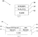
- a layer structure 10 which has a substrate 12, a crystalline bixbyite oxide layer 14 and a metal-containing layer 16.
- the substrate 12 is on-axis silicon, thus it has ⁇ 100> crystal orientation.
- crystal orientation ⁇ 100> means the face of a cubic crystal structure and encompasses [100], [010] and [001] orientations using the Miller indices.
- References herein to Si (100) also encompass a silicon substrate 12 which is miscut by up to 20° towards another crystallographic direction, for example towards the (111) plane.
- Si ⁇ 100> is readily available in large volumes at relatively low cost because it is used for consumer electronics such as computer chips for processing, memory, or graphics.
- Si ⁇ 100> is also widely used for the electronic circuits which drive photonic devices, such as complementary metal-oxide semiconductors (CMOS), because of its high charge carrier mobility (higher than in other orientations of Si).
- CMOS complementary metal-oxide semiconductors
- the silicon substrate 12 may be monolithic; that is comprising bulk single crystal silicon throughout. Alternatively the silicon substrate 12 may also comprise porous silicon for some or all of its thickness, for example it may form a sublayer.
- the substrate 12 may include an upper portion which is porous with a lower portion that is non-porous.
- the substrate 12 may include one or more discrete, non-continuous portions that are porous with the remainder being non-porous (with bulk silicon properties).
- the portions may be non-continuous within the plane of a sublayer and/or through the thickness of the layer (horizontally and/or vertically in the sense of the growth direction). The portions may be distributed in a regular array or irregular pattern across the substrate 12, and/or through it.
- the porosity may be constant or variable within the porous regions. Where the porosity is variable it may be linearly varied through the thickness, or may be varied according to a different function such as quadratic, logarithmic or a step function.
- the substrate may comprise silicon-germanium (SiGe), for example Si 0.8 Ge 0.2 , or silicon on insulator (SOI).
- SiGe silicon-germanium
- SOI silicon on insulator
- a single crystal crystalline bixbyite oxide layer 14 is positioned, grown or deposited on the substrate 12.
- the crystalline bixbyite oxide layer 14 may be a rare earth oxide layer.
- the rare earth elements are scandium (Sc), yttrium (Y) and all of the lanthanoid series which is lanthanum (La), cerium (Ce), praseodymium (Pr), neodymium (Nd), promethium (Pm), samarium (Sm), europium (Eu), gadolinium (Gd), terbium (Tb), dysprosium (Dy), holmium (Ho), erbium (Er), thulium (Tm), ytterbium (Yb) and lutetium (Lu).
- the bixbyite oxides are bixbyite in crystal structure.
- Other bixbyite oxides include indium oxide (In 2 O 3 ), vanadium oxide (V 2 O 5 ), iron oxide (Fe 2 O 3 ), manganese oxide (Mn 2 O 3 ) and ternary compounds of a rare earth, a metal and oxygen (RE-M-O).
- the crystalline bixbyite oxide layer 14 is epitaxially deposited.
- a crystalline bixbyite oxide is deposited on a substrate 12, or another layer, at sufficient surface temperature, low enough oxygen concentration and slow enough growth rate it does not match the crystal orientation of the previous layer, depending on the orientation of the substrate 12 or previous layer. Instead it grows in a different orientation, a process called “epi Twist TM " by the inventors.
- the crystalline bixbyite oxide layer 14 grows in [110] orientation which has lower surface energy than [100] orientation.
- the present inventors have determined that only a single crystalline bixbyite oxide layer 14 is required to both change the crystal orientation and offer a suitable surface for subsequent layers. This is in contrast to prior art layered structures in which two crystalline bixbyite oxide (rare earth oxide) layers were required, for example as shown in Figure 1 , one to change the crystal orientation and the other to offer a surface with appropriate lattice matching and quality.
- it is quicker, cheaper and easier to grow one crystalline bixbyite oxide layer 14 than to grow two.
- there is one fewer interfaces between layers which means the risk of introduced defects or inter-layer strains is reduced.
- the single crystalline bixbyite oxide layer 14 makes it simpler to balance between surface energy and mismatch energy instead of using one layer to eliminate one of these and the other layer to manage the other.
- the crystalline bixbyite oxide layer 14 insulates the metal-containing layer 16 from the Si substrate 12 which prevents metal silicide forming.
- Such silicides would be particularly likely to form, without the crystalline bixbyite oxide layer 14, if metal were deposited at higher temperature in order to improve quality.
- Figure 3 illustrates a layer structure 10 with a substrate 12 comprising Si (100).
- the crystalline bixbyite oxide layer 14 comprises scandium oxide, Sc 2 O 3 , which grows in [111] orientation on Si (100).
- the metal-containing layer 16 comprises molybdenum, Mo, which grows in [110] orientation on Sc 2 O 3 (111).
- Mo molybdenum
- This produces high quality Mo which is therefore better for subsequent device layers.
- it is an effective reflective layer or back contact for a photonic device.
- the alignment of the surface atoms of the Mo (110) layer is favourable for growth of III-(RE)-N layers, such as AIN or AIScN, in the ⁇ 0001> direction.
- FIG. 4 is a Reflection High-Energy Electron Diffraction (RHEED) pattern of growth of Mo on Er 2 O 3 . Mo grows in [112] orientation on Er 2 O 3 (110). It can be seen that there are several bright streaks which denote diffraction of electrons, and these are not aligned with each other. This indicates that the surface of the layer is faceted rather than smooth.
- Figure 5 is a similar RHEED pattern for growth of Mo (110) on SC 2 O 3 (111), according to the present invention. It can be seen that there is one bright streak and two first order diffraction streaks, and that they are all parallel, denoting that the crystal quality is better than that seen in Figure 4 .
- Scandium oxide which is a rare earth oxide but not in the lanthanoid series of elements, surprisingly behaves differently to other crystalline bixbyite oxides, particularly rare earth oxides, in that its lowest energy orientation is [111] and so it grows in this orientation on Si (100).
- the preferred crystal orientation of a material is dependent on its surface energy and the lattice mismatch to the layer below. The arrangement of the atoms within the crystal is also a factor since this affects the spacing between atoms on different surfaces, and whether a surface has only oxygen atoms, only metal atoms or a combination of both.
- Sc is a smaller atom than the other rare earth elements and the lattice spacing of Sc 2 O 3 is smaller than for other crystalline bixbyite oxides.
- SC 2 O 3 (111) exhibits a greater lattice mismatch to Si (100): around -9%. For this reason the surface energy becomes the dominant factor to define crystal orientation whereas in crystalline bixbyite oxides which are better lattice matched to Si (100), for example up to ⁇ 2%, the lattice match is the dominant factor even though the surface energy in (110) orientation may be twice that in (111) orientation.
- the metal-containing layer 16 may be deposited, epitaxially or otherwise, or may be sputtered. Due to the crystallinity of the crystalline bixbyite oxide layer 14, it has a surface with beneficial orientation on which to grow or deposit the metal-containing layer 16. Such metal-containing layer 16 will therefore be more suitable to support the desired device.
- the metal-containing layer 16 has been described as Mo. Alternatively it may be any of the transition metals, such as tantalum (Ta), tungsten (W), platinum (Pt) or nickel (Ni), or a metal from any of groups III to VI of the periodic table, such as Al, Ga, Sn or Sb. Alternatively it may be an alloy between one or more metals and one or more non-metals.
- the transition metals such as tantalum (Ta), tungsten (W), platinum (Pt) or nickel (Ni)
- a metal from any of groups III to VI of the periodic table such as Al, Ga, Sn or Sb.
- it may be an alloy between one or more metals and one or more non-metals.
- Figure 6 illustrates a layered structure 10 with a substrate 12 comprising Si (100).
- the crystalline bixbyite oxide layer 14 comprises scandium oxide, Sc 2 O 3 , which grows in [111] orientation.
- the metal-containing layer 16 is a III-V semiconductor, which is an alloy of one or more group III material with one or more group V material.
- the III-V semiconductor may also include a rare earth, for example being a III-RE-N material.
- the III-V may be a binary or ternary alloy such as GaN, AIN, InGaN, AIGaN, InN,AIScN, AlYN, GaScN, GaYN, AIYbN, GaYbN.
- Advantageously hexagonal III-V materials such as GaN grow in Wurtzitic phase on a (111) sub-layer.
- the metal-containing layer 16 is a III-N alloy in the [0001] orientation.
- the III-N may be wurtzite GaN.
- GaN is widely used for electronic and photonic applications.
- GaN is used in high electron mobility transistors (HEMTs) and for LED displays.
- HEMTs high electron mobility transistors
- GaN devices such as HEMTs are connected to Si-based CMOS electronics by wire, for example in telecommunication or internet base stations.
- the wiring presents a potential failure mode. It may also limit the speed of operation.
- the present invention permits the growth of GaN devices over Si (100) substrates which can also host CMOS electronics. Since the CMOS electronics and GaN devices are adjacent the wiring is obviated which removes the associated failure modes and means that device performance is governed by the devices themselves and not by the limitations of the connections.
- the ability to grow GaN (0001) means that the inherent charge is available, since the GaN is polar, which enables piezoelectric switching without doping.
- the GaN device may be configured to manage power, for example by performing step-down voltage conversion in a microprocessor.
- the GaN-based emitter or an array of GaN-based emitters, can be grown on Si (100) according to the present layered structure 10.
- Each emitter corresponds to one pixel of a display.
- the emitter or emitters can be controlled by electronic control components or devices which are also grown on or mounted on Si (100).
- the emitters and controls can be collocated, preferably adjacent, so that each pixel in an array can be individually addressed easily and directly.
- the pixels can be lit and switched off quickly and accurately.
- the layered structure 10 may be grown on part of a Si (100) substrate with electronic control components grown on another part of the Si (100) wafer as shown in Figure 7 .
- the second part of the wafer may include a bixbyite oxide layer 18 in [110] orientation.
- the bixbyite oxide layer 18 may comprise erbium oxide (Er 2 O 3 ) which twists to [110] orientation when grown on Si (100).
- a layer 20 can then be grown which is compatible with the [110] orientation.
- the layer 20 may comprise Mo (112).
- Figure 8 is an X-ray Power Diffraction (XRD) plot of a prior art III-N, AIN, grown directly on Er 2 O 3 . It can be seen that there is no XRD peak for AIN meaning the quality is very low. By contrast, when AIN is grown on Sc 2 O 3 , Figure 9 , there is a sharp peak which demonstrates good quality.
- XRD X-ray Power Diffraction
- Figure 10 illustrates a layered structure 10 with a substrate 12 comprising Si (100).
- a crystalline bixbyite oxide layer 14 in [111] orientation is grown on the substrate 12 as in previous examples.
- the metal-containing layer 16 comprises a ferroelectric material.
- the metal-containing layer 16 may include nitrogen.
- the ferroelectric material may be ScAIN or ScGaN.
- Such a layer is suitable for memory devices, ferroelectric switches, actuators and sensors. This is because III-(RE)-N materials combine piezoelectric, ferroelectric and pyroelectric properties.
- the layered structure 10 may be used for monolithically integrated RF filters which have Si CMOS. Also a GaN-based HEMT monolithically integrated with Si CMOS.
- the crystalline bixbyite oxide layer 14 has been described as scandium oxide in the [111] orientation, it may alternatively be any bixbyite oxide which twists to the [111] orientation when grown on Si (100).
- III-V metal-containing layer 16 has been described as GaN (0001) it could alternatively be AIN, InGaN, AIGaN, InN, AIScN, AlYN, GaScN, GaYN, AIYbN, GaYbN or any III-V alloy as known in the field.
Landscapes
- Chemical & Material Sciences (AREA)
- Engineering & Computer Science (AREA)
- Crystallography & Structural Chemistry (AREA)
- Materials Engineering (AREA)
- Metallurgy (AREA)
- Organic Chemistry (AREA)
- Inorganic Chemistry (AREA)
- Crystals, And After-Treatments Of Crystals (AREA)
- Physical Vapour Deposition (AREA)
- Physical Deposition Of Substances That Are Components Of Semiconductor Devices (AREA)
Abstract
Description
- A layered structure, particularly but not exclusively for growing III-N materials on Si (100) substrates or for growing metal-containing materials on Si (100) substrates.
- Many applications require a good quality III-N layer on which to grow or place one or more device layers. For example, a radio frequency (RF) switch may be grown epitaxially on a gallium nitride (GaN) layer in order to obtain suitable properties. Typically there are multiple layers on a substrate below the GaN layer.
- For epitaxial growth the crystal structure of a layer must match or be compatible with the layer below it. Each layer's crystal alignment is dictated by the lowest energy state of the material and the crystal orientation of the layer below it. Thus for homoepitaxy (growth of the same material as the preceding layer) the crystal orientation will be identical and for most heteroepitaxy (growth of a different material to the preceding layer) the crystal orientation will also be the same. Where the crystal structure of the subsequent layer is different, for example GaN in hexagonal form grown on silicon which is cubic, the subsequent layer grows in a compatible crystal orientation. Thus GaN grows in the polar [0001] orientation on Si (111) but grows in the semi-polar [11-20] orientation on a (110) rare earth oxide previous layer.
- It has previously been determined that crystalline rare earth oxides epitaxially grow with a different crystal orientation to the layer below them. This is called "epi Twist™" by the applicant. This can be used to grow a subsequent layer with a different crystal orientation to the substrate or a previous layer, provided that the lattice constants are approximately matched or that the upper layer has a lattice constant which is an integer multiple of the lattice constant of the lower layer.
- It is known to grow GaN (0001) on a Si (111) substrate using a double buffer,
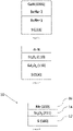
US7,012,016 . This is illustrated inFigure 1 . - It is also known, from
US8846504 , to grow GaN (11-20) on Si (100) by using a first gadolinium oxide layer which twists to (110) and a second erbium oxide layer which has a lattice constant closer to that of GaN (11-20). This is illustrated inFigure 2 . - Wurtzitic (c-direction) III-N materials such as GaN [0001] are preferable in the industry for electronic and photonic devices. For electronic devices, the polar nature of this form of GaN is required for a high electron mobility transistor (HEMT) to be fabricated. It is also preferable to use Si (100) substrates because they are widely available, and therefore cheap. They are also commercially available in larger diameters, up to 300mm, than other orientations of silicon such as Si (111). Furthermore Si (100) offers integration opportunities for photonic devices with electronic devices which are commonly produced on Si (100).
- One problem with current GaN chips is that to integrate them in a module with the driving electronics it is necessary to bond the GaN chip to a module on Si (100) and then connect them with wires. This introduces an additional failure mode and losses. It may also limit the speed of the device to the current capacity of the wire.
- The present invention seeks to provide a layer structure that prevents or overcomes the above-mentioned problems.
- The present invention provides a layered structure comprising: a substrate in [100] orientation or with a miscut up to 20°; a crystalline bixbyite oxide layer in [111] orientation positioned, grown or deposited on the substrate; and a metal-containing layer crystallographically matched to the crystalline bixbyite oxide layer.
- The crystalline bixbyite oxide layer in [111] orientation is advantageous because it enables high quality metal or metal-containing materials to be grown on substrates in [100] orientation. Advantageously photonic and power devices can be grown on such materials. For example, HEMT, RF switches, memory devices, actuators and sensors can all be grown, deposited or bonded onto high quality metal or metal-containing layers. Advantageously higher crystal quality improves device performance. For example, a single crystal orientation in the out of plane direction results in a stronger piezoelectric field in the desired crystallographic direction for RF filters and HEMTs.
- The crystalline bixbyite oxide layer may be directly positioned, grown or deposited on the substrate. Thus there are no intervening layers.
- The substrate may comprise silicon (Si). Advantageously Si (100) is widely available in large diameter wafers and is commonly used for electronic devices. Advantageously devices grown on a layered structure according to the present invention can be integrated with different devices directly grown on Si (100), known as heterointegration. Where a device grown on Si (100) is the driving power electronic device for that grown on the layered structure described herein this may obviate the need for wiring to connect the devices. Advantageously the device performance becomes the speed-limiting factor and not the wiring. Advantageously a potential failure mode is removed by omitting the wiring.
- The crystalline bixbyite oxide may be epitaxial. Advantageously it is easier to obtain good crystallinity by epitaxial deposition or growth.
- The crystalline bixbyite oxide may be a rare earth oxide. The crystalline bixbyite oxide may be scandium oxide (Sc2O3). Advantageously scandium oxide grows in [111] orientation on Si (100). Advantageously high quality metal or metal-containing materials can be grown in beneficial orientations on SC2O3 (111).
- The metal-containing layer may be epitaxial. Advantageously the metal-containing layer may be grown, deposited, immediately after the crystalline bixbyite oxide layer in the same tool. Advantageously the risk of contamination being introduced between the layers is reduced or eliminated.
- The metal-containing layer may be a III-N material. It may be gallium nitride (GaN). Advantageously this is a good material for HEMTs, for example. It may be aluminium nitride (AIN). This is a good material for piezoelectric devices such as radio frequency filters. It may be molybdenum (Mo). This is a good material for a back electrode of a filter or an effective reflective layer or back contact for a photonic device. It is also a good material for subsequent growth of III-(RE)-N materials for HEMT barriers in filters.
- The metal-containing layer may be sputtered. Advantageously the substrate with crystalline bixbyite oxide layer may be provided as a template. The metal-containing layer may be sputtered onto the template in the same or a different manufacturing location. For example, one party may produce the template and a second party may receive the template and sputter the metal-containing layer onto it. Alternatively the template may be produced in one location and the metal-containing layer may be sputtered onto it at another location by the same or an affiliated entity. In some instances sputtering the metal-containing layer may be cheaper and/or quicker than epitaxial growth or another deposition method.
- The sputtered metal-containing layer may be Mo. Advantageously Mo is commonly sputtered in the industry and therefore the process for sputtering Mo is mature and repeatable. Alternatively the sputtered material may be a III-N material such as GaN or AIN.
- The present invention also provides a photonic device comprising the layered structure as described. The photonic device may be a photoemitter; a photodetector; or a combined photoemitter and photodetector. It may be an LED or a micro-LED. Advantageously each of these applications benefits from the heterointegration benefits and/or the higher quality metal-containing layer of the present layered structure.
- The present invention also provides an electronic device; a radio frequency filter; or a high electron mobility transistor comprising the layered structure as described. Advantageously each of these applications benefits from the heterointegration benefits and/or the higher quality metal-containing layer of the present layered structure.
- The present invention also provides a method of fabricating a layered structure comprising steps to: epitaxially deposit a crystalline bixbyite oxide in [111] orientation on a substrate in [100] crystal orientation or miscut by up to 20°; and deposit a metal-containing layer on the crystalline bixbyite oxide layer.
- Advantageously the method provides higher quality metal or metal-containing materials on a commonly used orientation of substrate. Advantageously higher crystal quality improves device performance. For example, a single crystal orientation in the out of plane direction results in a stronger piezoelectric field in the desired crystallographic direction for RF filters and HEMTs.
- The step to deposit the metal-containing layer may comprise epitaxial deposition. Advantageously it can be performed immediately after the step to epitaxially deposit the crystalline bixbyite oxide layer, and in the same tool.
- Alternatively, the step to deposit the metal-containing layer may comprise sputtering. Advantageously this layer can be added at a different time and/or location. Advantageously sputtering is a mature process in the industry providing cheap and repeatable results.
- The present invention will be more fully described by way of example with reference to the accompanying drawings, in which:
-
Figure 1 is a prior art layer stack for growing III-N on silicon; -
Figure 2 is a prior art layer stack for growing III-N on silicon; -
Figure 3 is a layer stack according to the present invention; -
Figure 4 is a RHEED plot of prior art growth of Mo on a rare earth oxide; -
Figure 5 is a RHEED plot of growth of Mo on a rare earth oxide according to the present invention; -
Figure 6 is a layer stack according to the present invention; -
Figure 7 is a layer stack according to the present invention. -
Figure 8 is an XRD plot of prior art growth of AIN on a rare earth oxide; -
Figure 9 is an XRD plot of growth of AIN on a rare earth oxide according to the present invention; and -
Figure 10 is a layer stack according to the present invention. - Throughout this disclosure, as will be understood by the skilled reader, crystal orientation <100> means the face of a cubic crystal structure and encompasses [100], [010] and [001] orientations using the Miller indices. Similarly <0001> encompasses [0001] and [000-1] except if the material polarity is critical. Integer multiples of any one or more of the indices are equivalent to the unitary version of the index. For example, (222) is equivalent to, the same as, (111).
- The invention will now be described more particularly with reference to
Figure 3 . Alayer structure 10 is shown which has asubstrate 12, a crystallinebixbyite oxide layer 14 and a metal-containinglayer 16. Thesubstrate 12 is on-axis silicon, thus it has <100> crystal orientation. As will be understood by the skilled reader, crystal orientation <100> means the face of a cubic crystal structure and encompasses [100], [010] and [001] orientations using the Miller indices. References herein to Si (100) also encompass asilicon substrate 12 which is miscut by up to 20° towards another crystallographic direction, for example towards the (111) plane. - Si <100> is readily available in large volumes at relatively low cost because it is used for consumer electronics such as computer chips for processing, memory, or graphics. Si <100> is also widely used for the electronic circuits which drive photonic devices, such as complementary metal-oxide semiconductors (CMOS), because of its high charge carrier mobility (higher than in other orientations of Si). There is therefore an integration benefit to be gained by growing the photonic device on Si <100>, with suitable layers in between, if sufficient crystal quality can be obtained.
- The
silicon substrate 12 may be monolithic; that is comprising bulk single crystal silicon throughout. Alternatively thesilicon substrate 12 may also comprise porous silicon for some or all of its thickness, for example it may form a sublayer. Thesubstrate 12 may include an upper portion which is porous with a lower portion that is non-porous. Alternatively thesubstrate 12 may include one or more discrete, non-continuous portions that are porous with the remainder being non-porous (with bulk silicon properties). The portions may be non-continuous within the plane of a sublayer and/or through the thickness of the layer (horizontally and/or vertically in the sense of the growth direction). The portions may be distributed in a regular array or irregular pattern across thesubstrate 12, and/or through it. The porosity may be constant or variable within the porous regions. Where the porosity is variable it may be linearly varied through the thickness, or may be varied according to a different function such as quadratic, logarithmic or a step function. - Alternatively the substrate may comprise silicon-germanium (SiGe), for example Si0.8Ge0.2, or silicon on insulator (SOI).
- A single crystal crystalline
bixbyite oxide layer 14 is positioned, grown or deposited on thesubstrate 12. The crystallinebixbyite oxide layer 14 may be a rare earth oxide layer. The rare earth elements are scandium (Sc), yttrium (Y) and all of the lanthanoid series which is lanthanum (La), cerium (Ce), praseodymium (Pr), neodymium (Nd), promethium (Pm), samarium (Sm), europium (Eu), gadolinium (Gd), terbium (Tb), dysprosium (Dy), holmium (Ho), erbium (Er), thulium (Tm), ytterbium (Yb) and lutetium (Lu). The bixbyite oxides are bixbyite in crystal structure. Other bixbyite oxides include indium oxide (In2O3), vanadium oxide (V2O5), iron oxide (Fe2O3), manganese oxide (Mn2O3) and ternary compounds of a rare earth, a metal and oxygen (RE-M-O). - Preferably the crystalline
bixbyite oxide layer 14 is epitaxially deposited. When a crystalline bixbyite oxide is deposited on asubstrate 12, or another layer, at sufficient surface temperature, low enough oxygen concentration and slow enough growth rate it does not match the crystal orientation of the previous layer, depending on the orientation of thesubstrate 12 or previous layer. Instead it grows in a different orientation, a process called "epi Twist™" by the inventors. When growing most crystalline bixbyite oxides on Si (100) the crystallinebixbyite oxide layer 14 grows in [110] orientation which has lower surface energy than [100] orientation. - Advantageously the present inventors have determined that only a single crystalline
bixbyite oxide layer 14 is required to both change the crystal orientation and offer a suitable surface for subsequent layers. This is in contrast to prior art layered structures in which two crystalline bixbyite oxide (rare earth oxide) layers were required, for example as shown inFigure 1 , one to change the crystal orientation and the other to offer a surface with appropriate lattice matching and quality. Advantageously it is quicker, cheaper and easier to grow one crystallinebixbyite oxide layer 14 than to grow two. Advantageously there is one fewer interfaces between layers which means the risk of introduced defects or inter-layer strains is reduced. The single crystallinebixbyite oxide layer 14 makes it simpler to balance between surface energy and mismatch energy instead of using one layer to eliminate one of these and the other layer to manage the other. - Advantageously the crystalline
bixbyite oxide layer 14 insulates the metal-containinglayer 16 from theSi substrate 12 which prevents metal silicide forming. Such silicides would be particularly likely to form, without the crystallinebixbyite oxide layer 14, if metal were deposited at higher temperature in order to improve quality. -
Figure 3 illustrates alayer structure 10 with asubstrate 12 comprising Si (100). The crystallinebixbyite oxide layer 14 comprises scandium oxide, Sc2O3, which grows in [111] orientation on Si (100). The metal-containinglayer 16 comprises molybdenum, Mo, which grows in [110] orientation on Sc2O3 (111). Advantageously this produces high quality Mo which is therefore better for subsequent device layers. This means, for example, that it forms an efficient back electrode for a filter. Alternatively it is an effective reflective layer or back contact for a photonic device. The alignment of the surface atoms of the Mo (110) layer is favourable for growth of III-(RE)-N layers, such as AIN or AIScN, in the <0001> direction. Advantageously nitride layers grown on Mo (110) demonstrate better crystal quality than those grown on Mo (112).Figure 4 is a Reflection High-Energy Electron Diffraction (RHEED) pattern of growth of Mo on Er2O3. Mo grows in [112] orientation on Er2O3 (110). It can be seen that there are several bright streaks which denote diffraction of electrons, and these are not aligned with each other. This indicates that the surface of the layer is faceted rather than smooth.Figure 5 is a similar RHEED pattern for growth of Mo (110) on SC2O3 (111), according to the present invention. It can be seen that there is one bright streak and two first order diffraction streaks, and that they are all parallel, denoting that the crystal quality is better than that seen inFigure 4 . - Scandium oxide, which is a rare earth oxide but not in the lanthanoid series of elements, surprisingly behaves differently to other crystalline bixbyite oxides, particularly rare earth oxides, in that its lowest energy orientation is [111] and so it grows in this orientation on Si (100). The preferred crystal orientation of a material is dependent on its surface energy and the lattice mismatch to the layer below. The arrangement of the atoms within the crystal is also a factor since this affects the spacing between atoms on different surfaces, and whether a surface has only oxygen atoms, only metal atoms or a combination of both. Sc is a smaller atom than the other rare earth elements and the lattice spacing of Sc2O3 is smaller than for other crystalline bixbyite oxides. Therefore SC2O3 (111) exhibits a greater lattice mismatch to Si (100): around -9%. For this reason the surface energy becomes the dominant factor to define crystal orientation whereas in crystalline bixbyite oxides which are better lattice matched to Si (100), for example up to ±2%, the lattice match is the dominant factor even though the surface energy in (110) orientation may be twice that in (111) orientation.
- The metal-containing
layer 16 may be deposited, epitaxially or otherwise, or may be sputtered. Due to the crystallinity of the crystallinebixbyite oxide layer 14, it has a surface with beneficial orientation on which to grow or deposit the metal-containinglayer 16. Such metal-containinglayer 16 will therefore be more suitable to support the desired device. - The metal-containing
layer 16 has been described as Mo. Alternatively it may be any of the transition metals, such as tantalum (Ta), tungsten (W), platinum (Pt) or nickel (Ni), or a metal from any of groups III to VI of the periodic table, such as Al, Ga, Sn or Sb. Alternatively it may be an alloy between one or more metals and one or more non-metals. -
Figure 6 illustrates alayered structure 10 with asubstrate 12 comprising Si (100). The crystallinebixbyite oxide layer 14 comprises scandium oxide, Sc2O3, which grows in [111] orientation. The metal-containinglayer 16 is a III-V semiconductor, which is an alloy of one or more group III material with one or more group V material. Optionally the III-V semiconductor may also include a rare earth, for example being a III-RE-N material. The III-V may be a binary or ternary alloy such as GaN, AIN, InGaN, AIGaN, InN,AIScN, AlYN, GaScN, GaYN, AIYbN, GaYbN. Advantageously hexagonal III-V materials such as GaN grow in Wurtzitic phase on a (111) sub-layer. - The metal-containing
layer 16 is a III-N alloy in the [0001] orientation. For example, the III-N may be wurtzite GaN. GaN is widely used for electronic and photonic applications. For example, GaN is used in high electron mobility transistors (HEMTs) and for LED displays. - Currently GaN devices such as HEMTs are connected to Si-based CMOS electronics by wire, for example in telecommunication or internet base stations. The wiring presents a potential failure mode. It may also limit the speed of operation. The present invention permits the growth of GaN devices over Si (100) substrates which can also host CMOS electronics. Since the CMOS electronics and GaN devices are adjacent the wiring is obviated which removes the associated failure modes and means that device performance is governed by the devices themselves and not by the limitations of the connections. Advantageously the ability to grow GaN (0001) means that the inherent charge is available, since the GaN is polar, which enables piezoelectric switching without doping. The GaN device may be configured to manage power, for example by performing step-down voltage conversion in a microprocessor.
- Similarly, for LED or µLED applications the GaN-based emitter, or an array of GaN-based emitters, can be grown on Si (100) according to the present
layered structure 10. Each emitter corresponds to one pixel of a display. The emitter or emitters can be controlled by electronic control components or devices which are also grown on or mounted on Si (100). Thus the emitters and controls can be collocated, preferably adjacent, so that each pixel in an array can be individually addressed easily and directly. Advantageously the pixels can be lit and switched off quickly and accurately. - For example, the layered
structure 10 may be grown on part of a Si (100) substrate with electronic control components grown on another part of the Si (100) wafer as shown inFigure 7 . The second part of the wafer may include abixbyite oxide layer 18 in [110] orientation. Thebixbyite oxide layer 18 may comprise erbium oxide (Er2O3) which twists to [110] orientation when grown on Si (100). Alayer 20 can then be grown which is compatible with the [110] orientation. For example, thelayer 20 may comprise Mo (112). -
Figure 8 is an X-ray Power Diffraction (XRD) plot of a prior art III-N, AIN, grown directly on Er2O3. It can be seen that there is no XRD peak for AIN meaning the quality is very low. By contrast, when AIN is grown on Sc2O3,Figure 9 , there is a sharp peak which demonstrates good quality. -
Figure 10 illustrates alayered structure 10 with asubstrate 12 comprising Si (100). A crystallinebixbyite oxide layer 14 in [111] orientation is grown on thesubstrate 12 as in previous examples. The metal-containinglayer 16 comprises a ferroelectric material. The metal-containinglayer 16 may include nitrogen. For example, the ferroelectric material may be ScAIN or ScGaN. Such a layer is suitable for memory devices, ferroelectric switches, actuators and sensors. This is because III-(RE)-N materials combine piezoelectric, ferroelectric and pyroelectric properties. - The layered
structure 10 may be used for monolithically integrated RF filters which have Si CMOS. Also a GaN-based HEMT monolithically integrated with Si CMOS. - Although the crystalline
bixbyite oxide layer 14 has been described as scandium oxide in the [111] orientation, it may alternatively be any bixbyite oxide which twists to the [111] orientation when grown on Si (100). - Although the III-V metal-containing
layer 16 has been described as GaN (0001) it could alternatively be AIN, InGaN, AIGaN, InN, AIScN, AlYN, GaScN, GaYN, AIYbN, GaYbN or any III-V alloy as known in the field.
Claims (15)
- A layered structure (10) comprising:• a substrate (12) in [100] crystal orientation or with a miscut up to 20°;• a crystalline bixbyite oxide layer (14) in [111] orientation positioned, grown or deposited on the substrate (12); and• a metal-containing layer (16) crystallographically matched to the crystalline bixbyite oxide layer (14).
- A layered structure (10) as claimed in claim 1 wherein the substrate (12) comprises silicon.
- A layered structure (10) as claimed in claim 1 or claim 2 wherein the crystalline bixbyite oxide layer (14) is epitaxial.
- A layered structure (10) as claimed in any preceding claim wherein the crystalline bixbyite oxide layer (14) is a crystalline rare earth oxide layer (14).
- A layered structure (10) as claimed in any preceding claim wherein the crystalline bixbyite oxide layer (14) is scandium oxide (Sc2O3).
- A layered structure as claimed in any preceding claim wherein the metal-containing layer (16) is epitaxial.
- A layered structure (10) as claimed in claim 6 wherein the metal-containing layer (16) is a III-N material; GaN; AIN; or molybdenum.
- A layered structure (10) as claimed in any of claims 1 to 5 wherein the metal-containing layer (16) is sputtered.
- A layered structure (10) as claimed in claim 8 wherein the metal-containing layer (16) is molybdenum; III-N; AIN; GaN.
- A photonic device comprising the layered structure (10) as claimed in any preceding claim.
- A photonic device as claimed in claim 10 wherein the photonic device is a photoemitter; a photodetector; a combined photoemitter and photodetector; a light emitting diode (LED), or a micro-light emitting diode (µLED).
- An electronic device; a radio frequency (RF) filter; or a high electron mobility transistor (HEMT) comprising the layered structure (10) as claimed in any of claims 1 to 9.
- A method of fabricating a layered structure (10) comprising steps to:• epitaxially deposit a crystalline bixbyite oxide (14) in [111] orientation on a substrate (12) in [100] crystal orientation; and• deposit a metal-containing layer (16) on the crystalline bixbyite oxide layer (14).
- A method as claimed in claim 13 wherein the step to deposit the metal-containing layer (16) comprises epitaxial deposition.
- A method as claimed in claim 13 wherein the step to deposit the metal-containing layer (16) comprises sputtering.
Applications Claiming Priority (1)
| Application Number | Priority Date | Filing Date | Title |
|---|---|---|---|
| GB2106335.9A GB2606356A (en) | 2021-05-04 | 2021-05-04 | A layered structure |
Publications (1)
| Publication Number | Publication Date |
|---|---|
| EP4086939A1 true EP4086939A1 (en) | 2022-11-09 |
Family
ID=76301046
Family Applications (1)
| Application Number | Title | Priority Date | Filing Date |
|---|---|---|---|
| EP22169996.0A Pending EP4086939A1 (en) | 2021-05-04 | 2022-04-26 | A layered structure including an intermediate bixbyite oxide layer |
Country Status (6)
| Country | Link |
|---|---|
| US (1) | US12382690B2 (en) |
| EP (1) | EP4086939A1 (en) |
| JP (1) | JP2022172468A (en) |
| KR (1) | KR20220150836A (en) |
| CN (2) | CN218299801U (en) |
| GB (1) | GB2606356A (en) |
Cited By (2)
| Publication number | Priority date | Publication date | Assignee | Title |
|---|---|---|---|---|
| WO2024260593A1 (en) | 2023-06-22 | 2024-12-26 | Iqe Plc | A semiconductor structure |
| WO2024260670A1 (en) * | 2023-06-22 | 2024-12-26 | Iqe Plc | Semiconductor structure and method for forming a semiconductor structure |
Families Citing this family (2)
| Publication number | Priority date | Publication date | Assignee | Title |
|---|---|---|---|---|
| FR3106934B1 (en) * | 2020-02-05 | 2022-07-22 | Thales Sa | DEVICE COMPRISING A SET OF JOSEPHSON JUNCTIONS, SYSTEM COMPRISING SUCH DEVICE AND METHOD FOR USING SUCH DEVICE |
| GB2622272B (en) * | 2022-09-12 | 2024-11-13 | Iqe Plc | A semiconductor structure |
Citations (4)
| Publication number | Priority date | Publication date | Assignee | Title |
|---|---|---|---|---|
| US7012016B2 (en) | 2003-11-18 | 2006-03-14 | Shangjr Gwo | Method for growing group-III nitride semiconductor heterostructure on silicon substrate |
| US20130334536A1 (en) * | 2012-06-13 | 2013-12-19 | Rytis Dargis | SINGLE-CRYSTAL REO BUFFER ON AMORPHOUS SiOx |
| US8846504B1 (en) | 2013-11-08 | 2014-09-30 | Translucent, Inc. | GaN on Si(100) substrate using epi-twist |
| US20190227233A1 (en) * | 2018-01-19 | 2019-07-25 | Iqe Plc | RE-based Integrated Photonic and Electronic Layered Structures |
Family Cites Families (11)
| Publication number | Priority date | Publication date | Assignee | Title |
|---|---|---|---|---|
| US5937274A (en) * | 1995-01-31 | 1999-08-10 | Hitachi, Ltd. | Fabrication method for AlGaIn NPAsSb based devices |
| US8106381B2 (en) * | 2006-10-18 | 2012-01-31 | Translucent, Inc. | Semiconductor structures with rare-earths |
| US20110284048A1 (en) * | 2010-04-01 | 2011-11-24 | Hi - Z Technology, Inc. | Multi-layer superlattice quantum well thermoelectric material and module |
| US8823055B2 (en) * | 2012-12-17 | 2014-09-02 | Translucent, Inc. | REO/ALO/A1N template for III-N material growth on silicon |
| US10923345B2 (en) * | 2016-03-23 | 2021-02-16 | Iqe Plc | Epitaxial metal oxide as buffer for epitaxial III-V layers |
| US10132769B2 (en) * | 2016-07-13 | 2018-11-20 | Vaon, Llc | Doped, metal oxide-based chemical sensors |
| US10128350B2 (en) * | 2016-09-22 | 2018-11-13 | Iqe Plc | Integrated epitaxial metal electrodes |
| CN109494287B (en) * | 2017-09-11 | 2021-03-26 | 隆达电子股份有限公司 | Micro light-emitting diode structure and manufacturing method of micro light-emitting diode |
| US11757008B2 (en) | 2018-02-15 | 2023-09-12 | Iqe Plc | Electronic device with 2-dimensional electron gas between polar-oriented rare-earth oxide layer grown over a semiconductor |
| EP3766104A1 (en) * | 2018-03-12 | 2021-01-20 | Solar Junction Corporation | Chirped distributed bragg reflectors for photovoltaic cells and other light absorption devices |
| US11063114B2 (en) | 2018-11-20 | 2021-07-13 | Iqe Plc | III-N to rare earth transition in a semiconductor structure |
-
2021
- 2021-05-04 GB GB2106335.9A patent/GB2606356A/en not_active Withdrawn
-
2022
- 2022-04-26 EP EP22169996.0A patent/EP4086939A1/en active Pending
- 2022-04-29 CN CN202221039440.4U patent/CN218299801U/en active Active
- 2022-04-29 CN CN202210471897.0A patent/CN115377205A/en active Pending
- 2022-05-02 US US17/734,549 patent/US12382690B2/en active Active
- 2022-05-02 JP JP2022076219A patent/JP2022172468A/en active Pending
- 2022-05-03 KR KR1020220054778A patent/KR20220150836A/en active Pending
Patent Citations (4)
| Publication number | Priority date | Publication date | Assignee | Title |
|---|---|---|---|---|
| US7012016B2 (en) | 2003-11-18 | 2006-03-14 | Shangjr Gwo | Method for growing group-III nitride semiconductor heterostructure on silicon substrate |
| US20130334536A1 (en) * | 2012-06-13 | 2013-12-19 | Rytis Dargis | SINGLE-CRYSTAL REO BUFFER ON AMORPHOUS SiOx |
| US8846504B1 (en) | 2013-11-08 | 2014-09-30 | Translucent, Inc. | GaN on Si(100) substrate using epi-twist |
| US20190227233A1 (en) * | 2018-01-19 | 2019-07-25 | Iqe Plc | RE-based Integrated Photonic and Electronic Layered Structures |
Cited By (2)
| Publication number | Priority date | Publication date | Assignee | Title |
|---|---|---|---|---|
| WO2024260593A1 (en) | 2023-06-22 | 2024-12-26 | Iqe Plc | A semiconductor structure |
| WO2024260670A1 (en) * | 2023-06-22 | 2024-12-26 | Iqe Plc | Semiconductor structure and method for forming a semiconductor structure |
Also Published As
| Publication number | Publication date |
|---|---|
| JP2022172468A (en) | 2022-11-16 |
| US20220359668A1 (en) | 2022-11-10 |
| KR20220150836A (en) | 2022-11-11 |
| CN218299801U (en) | 2023-01-13 |
| US12382690B2 (en) | 2025-08-05 |
| CN115377205A (en) | 2022-11-22 |
| GB2606356A (en) | 2022-11-09 |
| GB202106335D0 (en) | 2021-06-16 |
Similar Documents
| Publication | Publication Date | Title |
|---|---|---|
| US12382690B2 (en) | Structure and method using a single crystalline bixbyite oxide layer in a orientation | |
| TWI720050B (en) | Layer structures for rf filters fabricated using rare earth oxides and epitaxial aluminum nitride and methods of forming the same | |
| US7612361B2 (en) | Method of growing a nitride single crystal on silicon wafer, nitride semiconductor light emitting diode manufactured using the same and the manufacturing method | |
| TWI725143B (en) | Layer structure with epitaxial metal oxide as buffer for epitaxial layers | |
| US9735318B2 (en) | Epitaxial hexagonal materials on IBAD-textured substrates | |
| EP2105973A1 (en) | Iii nitride compound semiconductor element and method for manufacturing the same, iii nitride compound semiconductor light emitting element and method for manufacturing the same, and lamp | |
| EP2200099A1 (en) | Group iii nitride semiconductor light-emitting device, method for manufacturing the same, and lamp | |
| US20190044029A1 (en) | Mutilayer structure containing a crystal matching layer for increased semiconductor device performance | |
| EP0551721A2 (en) | Gallium nitride base semiconductor device and method of fabricating the same | |
| TW201543547A (en) | Crystalline laminated structure and semiconductor device | |
| KR101422300B1 (en) | Composite substrate, and method for the production of a composite substrate | |
| WO2014050793A1 (en) | Semiconductor device or crystal, and method for producing semiconductor device or crystal | |
| EP3516681A1 (en) | Integrated epitaxial metal electrodes | |
| JP2016081946A (en) | Semiconductor structure and semiconductor device | |
| US10615141B2 (en) | Pnictide buffer structures and devices for GaN base applications | |
| EP4732327A1 (en) | A semiconductor structure | |
| JP4682541B2 (en) | Semiconductor crystal growth method | |
| US12057307B2 (en) | Group-III element nitride semiconductor substrate | |
| TW202105461A (en) | Integrated epitaxial metal electrodes | |
| US20260047161A1 (en) | A semiconductor structure | |
| JP2025535482A (en) | Heterostructures, devices and methods for forming heterostructures | |
| JP2001294500A (en) | Gallium nitride based compound semiconductor crystal growth method | |
| US20240347604A1 (en) | Group iii element nitride semiconductor substrate, epitaxial substrate, and functional element | |
| WO2025261627A1 (en) | Semiconductor structures | |
| WO2007129623A1 (en) | Gallium nitride compound semiconductor, light-emitting device, illuminating device, and method for producing gallium nitride compound semiconductor |
Legal Events
| Date | Code | Title | Description |
|---|---|---|---|
| PUAI | Public reference made under article 153(3) epc to a published international application that has entered the european phase |
Free format text: ORIGINAL CODE: 0009012 |
|
| STAA | Information on the status of an ep patent application or granted ep patent |
Free format text: STATUS: THE APPLICATION HAS BEEN PUBLISHED |
|
| AK | Designated contracting states |
Kind code of ref document: A1 Designated state(s): AL AT BE BG CH CY CZ DE DK EE ES FI FR GB GR HR HU IE IS IT LI LT LU LV MC MK MT NL NO PL PT RO RS SE SI SK SM TR |
|
| STAA | Information on the status of an ep patent application or granted ep patent |
Free format text: STATUS: REQUEST FOR EXAMINATION WAS MADE |
|
| P01 | Opt-out of the competence of the unified patent court (upc) registered |
Effective date: 20230321 |
|
| 17P | Request for examination filed |
Effective date: 20230605 |
|
| RBV | Designated contracting states (corrected) |
Designated state(s): AL AT BE BG CH CY CZ DE DK EE ES FI FR GB GR HR HU IE IS IT LI LT LU LV MC MK MT NL NO PL PT RO RS SE SI SK SM TR |