EP4086907A1 - Hot and hazardous indicator on solid state drives - Google Patents
Hot and hazardous indicator on solid state drives Download PDFInfo
- Publication number
- EP4086907A1 EP4086907A1 EP22165655.6A EP22165655A EP4086907A1 EP 4086907 A1 EP4086907 A1 EP 4086907A1 EP 22165655 A EP22165655 A EP 22165655A EP 4086907 A1 EP4086907 A1 EP 4086907A1
- Authority
- EP
- European Patent Office
- Prior art keywords
- node
- coupled
- timer circuit
- circuit
- timer
- Prior art date
- Legal status (The legal status is an assumption and is not a legal conclusion. Google has not performed a legal analysis and makes no representation as to the accuracy of the status listed.)
- Granted
Links
Images




Classifications
-
- G—PHYSICS
- G11—INFORMATION STORAGE
- G11C—STATIC STORES
- G11C5/00—Details of stores covered by group G11C11/00
-
- H—ELECTRICITY
- H02—GENERATION; CONVERSION OR DISTRIBUTION OF ELECTRIC POWER
- H02H—EMERGENCY PROTECTIVE CIRCUIT ARRANGEMENTS
- H02H5/00—Emergency protective circuit arrangements for automatic disconnection directly responsive to an undesired change from normal non-electric working conditions with or without subsequent reconnection
- H02H5/04—Emergency protective circuit arrangements for automatic disconnection directly responsive to an undesired change from normal non-electric working conditions with or without subsequent reconnection responsive to abnormal temperature
-
- G—PHYSICS
- G06—COMPUTING OR CALCULATING; COUNTING
- G06F—ELECTRIC DIGITAL DATA PROCESSING
- G06F1/00—Details not covered by groups G06F3/00 - G06F13/00 and G06F21/00
- G06F1/16—Constructional details or arrangements
- G06F1/20—Cooling means
- G06F1/206—Cooling means comprising thermal management
-
- G—PHYSICS
- G06—COMPUTING OR CALCULATING; COUNTING
- G06F—ELECTRIC DIGITAL DATA PROCESSING
- G06F1/00—Details not covered by groups G06F3/00 - G06F13/00 and G06F21/00
- G06F1/26—Power supply means, e.g. regulation thereof
- G06F1/30—Means for acting in the event of power-supply failure or interruption, e.g. power-supply fluctuations
-
- G—PHYSICS
- G06—COMPUTING OR CALCULATING; COUNTING
- G06F—ELECTRIC DIGITAL DATA PROCESSING
- G06F11/00—Error detection; Error correction; Monitoring
- G06F11/07—Responding to the occurrence of a fault, e.g. fault tolerance
- G06F11/16—Error detection or correction of the data by redundancy in hardware
- G06F11/20—Error detection or correction of the data by redundancy in hardware using active fault-masking, e.g. by switching out faulty elements or by switching in spare elements
- G06F11/2015—Redundant power supplies
-
- G—PHYSICS
- G06—COMPUTING OR CALCULATING; COUNTING
- G06F—ELECTRIC DIGITAL DATA PROCESSING
- G06F11/00—Error detection; Error correction; Monitoring
- G06F11/30—Monitoring
- G06F11/3003—Monitoring arrangements specially adapted to the computing system or computing system component being monitored
- G06F11/3034—Monitoring arrangements specially adapted to the computing system or computing system component being monitored where the computing system component is a storage system, e.g. DASD based or network based
-
- G—PHYSICS
- G06—COMPUTING OR CALCULATING; COUNTING
- G06F—ELECTRIC DIGITAL DATA PROCESSING
- G06F11/00—Error detection; Error correction; Monitoring
- G06F11/30—Monitoring
- G06F11/3003—Monitoring arrangements specially adapted to the computing system or computing system component being monitored
- G06F11/3037—Monitoring arrangements specially adapted to the computing system or computing system component being monitored where the computing system component is a memory, e.g. virtual memory, cache
-
- G—PHYSICS
- G06—COMPUTING OR CALCULATING; COUNTING
- G06F—ELECTRIC DIGITAL DATA PROCESSING
- G06F11/00—Error detection; Error correction; Monitoring
- G06F11/30—Monitoring
- G06F11/3003—Monitoring arrangements specially adapted to the computing system or computing system component being monitored
- G06F11/3044—Monitoring arrangements specially adapted to the computing system or computing system component being monitored where the computing system component is the mechanical casing of the computing system
-
- G—PHYSICS
- G06—COMPUTING OR CALCULATING; COUNTING
- G06F—ELECTRIC DIGITAL DATA PROCESSING
- G06F11/00—Error detection; Error correction; Monitoring
- G06F11/30—Monitoring
- G06F11/3058—Monitoring arrangements for monitoring environmental properties or parameters of the computing system or of the computing system component, e.g. monitoring of power, currents, temperature, humidity, position, vibrations
-
- G—PHYSICS
- G06—COMPUTING OR CALCULATING; COUNTING
- G06F—ELECTRIC DIGITAL DATA PROCESSING
- G06F11/00—Error detection; Error correction; Monitoring
- G06F11/30—Monitoring
- G06F11/32—Monitoring with visual or acoustical indication of the functioning of the machine
- G06F11/324—Display of status information
- G06F11/325—Display of status information by lamps or LED's
-
- G—PHYSICS
- G08—SIGNALLING
- G08B—SIGNALLING SYSTEMS, e.g. PERSONAL CALLING SYSTEMS; ORDER TELEGRAPHS; ALARM SYSTEMS
- G08B21/00—Alarms responsive to a single specified undesired or abnormal condition and not otherwise provided for
- G08B21/18—Status alarms
- G08B21/182—Level alarms, e.g. alarms responsive to variables exceeding a threshold
-
- G—PHYSICS
- G08—SIGNALLING
- G08B—SIGNALLING SYSTEMS, e.g. PERSONAL CALLING SYSTEMS; ORDER TELEGRAPHS; ALARM SYSTEMS
- G08B5/00—Visible signalling systems, e.g. visible personal calling systems or remote indication of seats occupied
- G08B5/22—Visible signalling systems, e.g. visible personal calling systems or remote indication of seats occupied using electric transmission; using electromagnetic transmission
- G08B5/36—Visible signalling systems, e.g. visible personal calling systems or remote indication of seats occupied using electric transmission; using electromagnetic transmission using visible light sources
- G08B5/38—Visible signalling systems, e.g. visible personal calling systems or remote indication of seats occupied using electric transmission; using electromagnetic transmission using visible light sources using flashing light
-
- G—PHYSICS
- G11—INFORMATION STORAGE
- G11C—STATIC STORES
- G11C16/00—Erasable programmable read-only memories
- G11C16/02—Erasable programmable read-only memories electrically programmable
- G11C16/06—Auxiliary circuits, e.g. for writing into memory
- G11C16/22—Safety or protection circuits preventing unauthorised or accidental access to memory cells
-
- G—PHYSICS
- G11—INFORMATION STORAGE
- G11C—STATIC STORES
- G11C16/00—Erasable programmable read-only memories
- G11C16/02—Erasable programmable read-only memories electrically programmable
- G11C16/06—Auxiliary circuits, e.g. for writing into memory
- G11C16/30—Power supply circuits
-
- G—PHYSICS
- G11—INFORMATION STORAGE
- G11C—STATIC STORES
- G11C16/00—Erasable programmable read-only memories
- G11C16/02—Erasable programmable read-only memories electrically programmable
- G11C16/06—Auxiliary circuits, e.g. for writing into memory
- G11C16/32—Timing circuits
-
- G—PHYSICS
- G11—INFORMATION STORAGE
- G11C—STATIC STORES
- G11C5/00—Details of stores covered by group G11C11/00
- G11C5/14—Power supply arrangements, e.g. power down, chip selection or deselection, layout of wirings or power grids, or multiple supply levels
- G11C5/141—Battery and back-up supplies
-
- G—PHYSICS
- G11—INFORMATION STORAGE
- G11C—STATIC STORES
- G11C5/00—Details of stores covered by group G11C11/00
- G11C5/14—Power supply arrangements, e.g. power down, chip selection or deselection, layout of wirings or power grids, or multiple supply levels
- G11C5/143—Detection of memory cassette insertion or removal; Continuity checks of supply or ground lines; Detection of supply variations, interruptions or levels ; Switching between alternative supplies
-
- G—PHYSICS
- G11—INFORMATION STORAGE
- G11C—STATIC STORES
- G11C7/00—Arrangements for writing information into, or reading information out from, a digital store
- G11C7/04—Arrangements for writing information into, or reading information out from, a digital store with means for avoiding disturbances due to temperature effects
-
- G—PHYSICS
- G11—INFORMATION STORAGE
- G11C—STATIC STORES
- G11C7/00—Arrangements for writing information into, or reading information out from, a digital store
- G11C7/24—Memory cell safety or protection circuits, e.g. arrangements for preventing inadvertent reading or writing; Status cells; Test cells
-
- H—ELECTRICITY
- H02—GENERATION; CONVERSION OR DISTRIBUTION OF ELECTRIC POWER
- H02H—EMERGENCY PROTECTIVE CIRCUIT ARRANGEMENTS
- H02H1/00—Details of emergency protective circuit arrangements
- H02H1/0007—Details of emergency protective circuit arrangements concerning the detecting means
-
- H—ELECTRICITY
- H05—ELECTRIC TECHNIQUES NOT OTHERWISE PROVIDED FOR
- H05B—ELECTRIC HEATING; ELECTRIC LIGHT SOURCES NOT OTHERWISE PROVIDED FOR; CIRCUIT ARRANGEMENTS FOR ELECTRIC LIGHT SOURCES, IN GENERAL
- H05B45/00—Circuit arrangements for operating light-emitting diodes [LED]
-
- G—PHYSICS
- G06—COMPUTING OR CALCULATING; COUNTING
- G06F—ELECTRIC DIGITAL DATA PROCESSING
- G06F2201/00—Indexing scheme relating to error detection, to error correction, and to monitoring
- G06F2201/81—Threshold
-
- H—ELECTRICITY
- H05—ELECTRIC TECHNIQUES NOT OTHERWISE PROVIDED FOR
- H05B—ELECTRIC HEATING; ELECTRIC LIGHT SOURCES NOT OTHERWISE PROVIDED FOR; CIRCUIT ARRANGEMENTS FOR ELECTRIC LIGHT SOURCES, IN GENERAL
- H05B45/00—Circuit arrangements for operating light-emitting diodes [LED]
- H05B45/30—Driver circuits
- H05B45/37—Converter circuits
- H05B45/3725—Switched mode power supply [SMPS]
-
- H—ELECTRICITY
- H05—ELECTRIC TECHNIQUES NOT OTHERWISE PROVIDED FOR
- H05B—ELECTRIC HEATING; ELECTRIC LIGHT SOURCES NOT OTHERWISE PROVIDED FOR; CIRCUIT ARRANGEMENTS FOR ELECTRIC LIGHT SOURCES, IN GENERAL
- H05B45/00—Circuit arrangements for operating light-emitting diodes [LED]
- H05B45/30—Driver circuits
- H05B45/395—Linear regulators
Definitions
- Embodiments generally relate to memory structures. More particularly, embodiments relate to a hot and hazardous indicator on solid state drives.
- a typical solid state drive has an enclosure that serves as a heatsink to dissipate heat generated by printed circuit board (PCB) components within the enclosure.
- the SSD may be designed to reduce the likelihood that the external surface temperature (e.g., "touch temperature”) of the enclosure will exceed a temperature that is unsafe to the human body.
- the SSD enclosure touch temperature may be monitored by firmware (FW) based on input data from hardware components such as a temperature sensor on the PCB, memory media and a memory controller. In such a case, the firmware reports the enclosure touch temperature to a log that is accessible by the end user (e.g., technician during replacement or debugging) using toolbox software. While the toolbox software solution may be suitable under certain circumstances, there remains considerable room for improvement.
- the toolbox software may retrieve incomplete, inaccurate and/or unreliable temperature readings.
- the technician may incorrectly check the temperature of the wrong SSD and assume that the hot or hazardous SSD is safe to touch. Additionally, once a hot and hazardous SSD is powered down, the toolbox software may be unusable.
- first SSD 10a has a safe touch temperature
- second SSD 10b has an unsafe touch temperature (e.g., has an enclosure temperature that exceeds a threshold such as 70°C and is therefore considered "hot")
- n th SSD 10n that has a safe touch temperature
- the SSDs 10 include indicators 12 (12a-12n) of whether the respective touch temperatures of the SSDs 10 are safe.
- a first indicator 12a is not activated to signify that the first SSD 10a has a safe touch temperature
- a second indicator 12b is activated (e.g., flashed, blinked) to signify that the second SSD 10b has an unsafe touch temperature
- an n th indicator 12n is not activated to signify that the n th SSD 10n has a safe temperature.
- the indicators 12 may be visual notification devices (e.g., light emitting diodes/LEDs).
- the second indicator 12b is an LED that is flashed (e.g., to emit light pulses) at a certain duty cycle (e.g., 10%) and frequency (e.g., 3Hz) when the enclosure temperature is unsafe.
- the illustrated SSDs 10 are safety-enhanced for several reasons.
- the indicators 12 may obviate any need for toolbox software, which may retrieve incomplete, inaccurate and/or unreliable temperature readings if temperature reporting firmware or hardware within the SSDs 10 malfunctions (e.g., due to power rail shorts, incorrect calibration).
- the indicators 12 reduce the likelihood that a technician may incorrectly check the temperature of the first SSD 10a or the n th SSD 10n and assume that the second SSD 10b is safe to touch.
- the indicators 12 may be operable even after the SSDs 10 are powered down, which is a significant advantage over toolbox software.
- FIG. 2 shows an SSD 20 that includes an enclosure 22, a non-volatile memory (NVM) device 24, a device controller 26 coupled to the NVM device 24, a capacitor 28, a backup voltage line 30 coupled to the capacitor 28, and a safety assembly 32.
- NVM non-volatile memory
- the safety assembly 32 may include a temperature comparator 21 (e.g., thermistor) positioned in a location to detect the heat 34 and an indicator 23 positioned in a location that is visible to end users when the SSD 20 is installed.
- a temperature comparator 21 e.g., thermistor
- the safety assembly 32 if the heat 34 causes the temperature of the enclosure 22 to exceed a threshold (e.g., 70°C so that the outer surface becomes unsafe to touch), the safety assembly 32 outputs light pulses 36 to alert nearby individuals (e.g., technicians) of the unsafe condition.
- a threshold e.g. 70°C so that the outer surface becomes unsafe to touch
- the capacitor 28 may be charged to a backup voltage (e.g., power loss imminent/PLI voltage) during operation of the SSD 20. Accordingly, the backup voltage may be used to power the safety assembly 32 when the SSD 20 is powered off (e.g., when traditional toolbox software is unusable to detect the hot and hazardous condition).
- the SSD 20 is safety-enhanced at least to the extent that the safety assembly 32 obviates any need for toolbox software, which may retrieve incomplete, inaccurate and/or unreliable temperature readings if temperature reporting firmware or hardware within the SSD 20 malfunctions. Moreover, the safety assembly 32 reduces the likelihood that a technician may incorrectly check the temperature of the wrong SSD (not shown) and assume that the SSD 20 is safe to touch. Additionally, the safety assembly 32 may be operable even after the SSD 20 is powered down, unlike toolbox software.
- the SSD 20 may be part of a memory device that includes non-volatile memory and/or volatile memory.
- Non-volatile memory is a storage medium that does not require power to maintain the state of data stored by the medium.
- the memory structure is a block addressable storage device, such as those based on NAND or NOR technologies.
- a storage device may also include future generation nonvolatile devices, such as a three-dimensional (3D) Xpoint memory device, or other byte addressable write-in-place nonvolatile memory devices.
- the storage device may be or may include memory devices that use silicon-oxide-nitride-oxide-silicon (SONOS) memory, electrically erasable programmable read-only memory (EEPROM), chalcogenide glass, multi-threshold level NAND flash memory, NOR flash memory, single or multilevel Phase Change Memory (PCM), a resistive memory, nanowire memory, ferroelectric transistor random access memory (FeTRAM), anti-ferroelectric memory, magnetoresistive random access memory (MRAM) memory that incorporates memristor technology, resistive memory including the metal oxide base, the oxygen vacancy base and the conductive bridge Random Access Memory (CB-RAM), or spin transfer torque (STT)-MRAM, a spintronic magnetic junction memory based device, a magnetic tunneling junction (MTJ) based device, a DW (Domain Wall) and SOT (Spin Orbit Transfer) based device, a thiristor based memory device, or a combination of any of the above, or other memory.
- 3D Xpoint memory may comprise a transistor-less stackable cross point architecture in which memory cells sit at the intersection of word lines and bit lines and are individually addressable and in which bit storage is based on a change in bulk resistance.
- a memory module with non-volatile memory may comply with one or more standards promulgated by the Joint Electron Device Engineering Council (JEDEC), such as JESD235, JESD218, JESD219, JESD220-1, JESD223B, JESD223-1, or other suitable standard (the JEDEC standards cited herein are available at jedec.org).
- JEDEC Joint Electron Device Engineering Council
- Volatile memory is a storage medium that requires power to maintain the state of data stored by the medium.
- volatile memory may include various types of random access memory (RAM), such as dynamic random access memory (DRAM) or static random access memory (SRAM).
- DRAM dynamic random access memory
- SRAM static random access memory
- DRAM of the memory modules complies with a standard promulgated by JEDEC, such as JESD79F for Double Data Rate (DDR) SDRAM, JESD79-2F for DDR2 SDRAM, JESD79-3F for DDR3 SDRAM, or JESD79-4A for DDR4 SDRAM (these standards are available at jedec.org).
- DDR-based standards and communication interfaces of the storage devices that implement such standards may be referred to as DDR-based interfaces.
- a safety assembly 40 is shown in which a timer circuit 42 includes an input node 44 (e.g., contact, pin, trace, connection) coupled to a backup voltage line 46, a reset node 48, and an output node 50.
- the safety assembly 40 may also include an indicator circuit 52 coupled to the output node 50 of the timer circuit 42.
- a temperature comparator circuit 54 is coupled to the reset node 48 of the timer circuit 42, wherein if an enclosure temperature (e.g., surface temperature of an SSD enclosure) exceeds a threshold while a backup voltage (e.g., PLI voltage) is present on the backup voltage line 46, the temperature comparator circuit 54 causes the timer circuit 42 to trigger light pulses from the indicator circuit 52.
- an enclosure temperature e.g., surface temperature of an SSD enclosure
- a backup voltage e.g., PLI voltage
- the timer circuit 42 includes a regulator 56 (e.g., low dropout/LDO or buck-boost regulator) including the input node 44, a regulator output node 58, and an enablement node 60. Additionally, the timer circuit 42 may include a timer device 62 (e.g., 555 timer integrated circuit/IC) having the output node 50, the reset node 48, and a timer input node 64 coupled to the regulator output node 58. The regulator 56 may convert the backup voltage (e.g., 35V) down to an operating voltage voltage (e.g., V cc of 3.3V) that is provided to the timer device 62 via a step-down voltage line 76.
- a regulator 56 e.g., low dropout/LDO or buck-boost regulator
- the timer circuit 42 may include a timer device 62 (e.g., 555 timer integrated circuit/IC) having the output node 50, the reset node 48, and a timer input no
- the enablement node 60 is coupled to a main voltage line 66.
- a lack of a main voltage (V main ) on the main voltage line 66 e.g., system power is off
- a presence of the main voltage on the main voltage line 66 disables the timer circuit 42 and the light pulses.
- the illustrated safety assembly 40 operates only when system power is off and while the backup voltage is present on the backup voltage line 46.
- the backup voltage may be provided by a capacitor 68 (e.g., aluminum electrolytic capacitor), which will discharge during operation of the safety assembly 40. Proper selection of the operating parameters of the timer device 62 may ensure that the light pulses are generated long enough for the enclosure temperature to fall below the safety threshold.
- the illustrated temperature comparator circuit 54 includes a temperature comparator device 70 (e.g., thermistor positioned adjacent to the enclosure and/or heat-generating components) coupled to a ground connection 72 (e.g., contact, pin, trace, node) and the reset node 48. Additionally, the temperature comparator circuit 54 may include a divider resistor 74 coupled to the reset node 48 and the step-down voltage line 76 (V LDO ) of the timer circuit 42.
- the indicator circuit 52 includes a switch 78 (e.g., metal oxide semiconductor field effect transistor/MOSFET) coupled to the output node 50 and the ground connection 72.
- an LED 80 is coupled to the switch 78 and a series resistor 82 is coupled to the LED 80 and the step-down voltage line 76 of the timer circuit 76.
- the LED 80 may be mounted in a position that is visible through the enclosure while the SSD is installed in a system such as, for example, a data storage server. Indeed, the LED 80 may be a standard component in EDSFF (Enterprise and Data Center SSD Form Factor) SSDs.
- the temperature comparator device 70 will transition to a high resistance or open state and activate the timer device 62 by pulling the reset node 48 high. Activating the timer device 62 causes the output node 50 to periodically activate the LED 80 via the switch 78.
- the indicator circuit 52 may be modified to include a speaker/buzzer instead of, or in addition to, the LED 80 to provide audible/sound notifications.
- FIG. 3B shows a safety assembly 90 that is the same as the safety assembly 40 ( FIG. 3A ) except that the enablement node 60 is coupled to the ground connection 72. Accordingly, the ground connection 72 enables the timer circuit 42 and the light pulses while when the system power is both powered off and powered on.
- the LED 80 may be an additional LED that is dedicated to the safety assembly 90 (e.g., not shared with other components of the SSD).
- FIG. 4 shows a plot 100 of a main voltage (V main ) curve 102, a backup voltage (V PLI ) curve 104, and a step-down voltage curve 106 (V LDO ).
- the safety assembly is not operating during a period 108 when the main voltage is present.
- the main voltage is turned off, the step-down voltage goes high, the backup voltage begins to drop (e.g., due to discharge of the PLI capacitor), and a period 110 begins.
- the backup voltage reaches the step-down voltage and the step-down voltage begins to drop along with the backup voltage.
- the safety assembly ceases operation.
- operating parameters such as the duty cycle and frequency of the LED are selected so that the period 110 is long enough for the enclosure to cool down to a safe temperature.
- FIG. 5 demonstrates in a plot 120 that with a 2000uF aluminum electrolytic capacitor charged to 20V, a 10% duty cycle and a blinking frequency of 3Hz, the safety assembly 40 ( FIG. 3A ) can operate for up to 55 seconds.
- a capacitor voltage value of 20V is chosen as empirical data shows that firmware can complete a PLI data dump before the PLI voltage drops below 20V from a full charge of 35V.
- a duty cycle value of 10% may minimize the energy needed to blink/flash the LED.
- an SSD having an E1.L form factor may have 100 seconds to cool down from 70°C to 50°C.
- the operating duration of the safety assembly may be further extended using techniques such as increasing the PLI capacitor capacitance, increasing the PLI voltage, using a buck-boost regulator, which will generate output voltages at lower input voltages and with better efficiency, and so forth.
- FIG. 6A shows a method 130 of operating a performance-enhanced safety assembly.
- the method 130 may generally be implemented in a safety assembly such as, for example, the safety assembly 40 ( FIG. 3A ), already discussed. More particularly, the method 130 may be implemented in configurable logic such as, for example, programmable logic arrays (PLAs), field-programmable gate arrays (FPGAs), complex programmable logic devices (CPLDs), in fixed-functionality hardware logic using circuit technology such as, for example, application-specific integrated circuit (ASIC), complementary metal oxide semiconductor (CMOS) or transistor-transistor logic (TTL) technology, or any combination thereof.
- PLAs programmable logic arrays
- FPGAs field-programmable gate arrays
- CPLDs complex programmable logic devices
- ASIC application-specific integrated circuit
- CMOS complementary metal oxide semiconductor
- TTL transistor-transistor logic
- Illustrated processing block 132 determines whether a main voltage is present on a main voltage line. If not, block 134 enables, via a lack of the main voltage on the main voltage line, a timer circuit and light pulses. In an embodiment, block 136 causes, by a temperature comparator circuit, the timer circuit to trigger the light pulses from an indicator circuit if an enclosure temperature exceeds a threshold while a backup voltage is present on a backup voltage line.
- the timer circuit includes an input node coupled to the backup voltage line, a reset node (e.g., input of the timer circuit), and an output node.
- the indicator circuit may be coupled to the output node of the timer circuit and the temperature comparator circuit may be coupled to the reset node of the timer circuit.
- the timer circuit includes a regulator including the input node, a regulator output node, and an enablement node and a timer device including the output node, the reset node, and a timer input node coupled to the regulator output node.
- the enablement node is coupled to the main voltage line. If it is determined at block 132 that the main voltage is present on the main voltage line, block 138 disables, via the presence of the main voltage on the main voltage line, the timer circuit and the light pulses.
- the method 130 therefore enhances performance and safety at least to the extent that the safety assembly obviates any need for toolbox software, which may retrieve incomplete, inaccurate and/or unreliable temperature readings if temperature reporting firmware or hardware within the SSD malfunctions. Moreover, the method 130 reduces the likelihood that a technician may incorrectly check the temperature of the wrong SSD and assume that the hot and hazardous SSD is safe to touch. Additionally, the method 130 is operable even after the SSD is powered off, unlike toolbox software.
- FIG. 6B shows another method 140 of operating a performance-enhanced safety assembly.
- the method 140 may generally be implemented in a safety assembly such as, for example, safety assembly 90 ( FIG. 3B ), already discussed. More particularly, the method 140 may be implemented in configurable logic such as, for example, PLAs, FPGAs, CPLDs, in fixed-functionality hardware logic using circuit technology such as, for example, ASIC, CMOS or TTL technology, or any combination thereof.
- Illustrated processing block 142 enables, via a ground connection, a timer circuit and light pulses.
- block 144 causes, by a temperature comparator circuit, the timer circuit to trigger the light pulses from an indicator circuit if an enclosure temperature exceeds a threshold while a backup voltage is present on a backup voltage line.
- the timer circuit includes an input node coupled to the backup voltage line, a reset node (e.g., input of the timer circuit), and an output node.
- the indicator circuit may be coupled to the output node of the timer circuit and the temperature comparator circuit may be coupled to the reset node of the timer circuit.
- the timer circuit includes a regulator including the input node, a regulator output node, and an enablement node and a timer device including the output node, the reset node, and a timer input node coupled to the regulator output node.
- the enablement node is coupled to the ground connection.
- the method 140 therefore enhances performance and safety at least to the extent that the safety assembly obviates any need for toolbox software, which may retrieve incomplete, inaccurate and/or unreliable temperature readings if temperature reporting firmware or hardware within the SSD malfunctions. Moreover, the method 140 reduces the likelihood that a technician may incorrectly check the temperature of the wrong SSD and assume that the hot and hazardous SSD is safe to touch. Additionally, the method 130 is operable when the SSD is both powered on and powered off, unlike toolbox software.
- Technology described herein therefore provides a visible indicator (e.g., located on the front of a drive to be user visible) of the drive running hot.
- the technology is firmware and software independent and it may operate even if firmware is not executing due to a severe failure.
- the technology also reduces the possibility of injuries due to human error reading the wrong SSD enclosure temperature from an SSD toolbox.
- the technology provides an alternative to thermal throttling, which may reduce performance or require additional airflow or heat pipe components to maintain performance (e.g., leading to increased cost and a lack of competitiveness).
- the technology enhances safety over regulatory warning labels that are not visible to the user when the SSD is assembled in the system.
- Embodiments are applicable for use with all types of semiconductor integrated circuit (“IC") chips.
- IC semiconductor integrated circuit
- Examples of these IC chips include but are not limited to processors, controllers, chipset components, programmable logic arrays (PLAs), memory chips, network chips, systems on chip (SoCs), SSD/NAND controller ASICs, and the like.
- PLAs programmable logic arrays
- SoCs systems on chip
- SSD/NAND controller ASICs solid state drive/NAND controller ASICs
- signal conductor lines are represented with lines. Some may be different, to indicate more constituent signal paths, have a number label, to indicate a number of constituent signal paths, and/or have arrows at one or more ends, to indicate primary information flow direction. This, however, should not be construed in a limiting manner.
- Any represented signal lines may actually comprise one or more signals that may travel in multiple directions and may be implemented with any suitable type of signal scheme, e.g., digital or analog lines implemented with differential pairs, optical fiber lines, and/or single-ended lines.
- Example sizes/models/values/ranges may have been given, although embodiments are not limited to the same. As manufacturing techniques (e.g., photolithography) mature over time, it is expected that devices of smaller size could be manufactured.
- well known power/ground connections to IC chips and other components may or may not be shown within the figures, for simplicity of illustration and discussion, and so as not to obscure certain aspects of the embodiments. Further, arrangements may be shown in block diagram form in order to avoid obscuring embodiments, and also in view of the fact that specifics with respect to implementation of such block diagram arrangements are highly dependent upon the platform within which the embodiment is to be implemented, i.e., such specifics should be well within purview of one skilled in the art.
- Coupled may be used herein to refer to any type of relationship, direct or indirect, between the components in question, and may apply to electrical, mechanical, fluid, optical, electromagnetic, electromechanical or other connections.
- first”, second, etc. may be used herein only to facilitate discussion, and carry no particular temporal or chronological significance unless otherwise indicated.
Landscapes
- Engineering & Computer Science (AREA)
- Theoretical Computer Science (AREA)
- Physics & Mathematics (AREA)
- General Physics & Mathematics (AREA)
- General Engineering & Computer Science (AREA)
- Computing Systems (AREA)
- Quality & Reliability (AREA)
- Mathematical Physics (AREA)
- Power Engineering (AREA)
- Business, Economics & Management (AREA)
- Emergency Management (AREA)
- Electromagnetism (AREA)
- Human Computer Interaction (AREA)
- Computer Security & Cryptography (AREA)
- Dc-Dc Converters (AREA)
Abstract
Description
- Embodiments generally relate to memory structures. More particularly, embodiments relate to a hot and hazardous indicator on solid state drives.
- A typical solid state drive (SSD) has an enclosure that serves as a heatsink to dissipate heat generated by printed circuit board (PCB) components within the enclosure. The SSD may be designed to reduce the likelihood that the external surface temperature (e.g., "touch temperature") of the enclosure will exceed a temperature that is unsafe to the human body. The SSD enclosure touch temperature may be monitored by firmware (FW) based on input data from hardware components such as a temperature sensor on the PCB, memory media and a memory controller. In such a case, the firmware reports the enclosure touch temperature to a log that is accessible by the end user (e.g., technician during replacement or debugging) using toolbox software. While the toolbox software solution may be suitable under certain circumstances, there remains considerable room for improvement.
- For example, if the temperature reporting firmware or hardware malfunctions (e.g., due to power rail shorts, incorrect calibration), the toolbox software may retrieve incomplete, inaccurate and/or unreliable temperature readings. Moreover, if a hot or hazardous SSD is installed in an array of SSDs, the technician may incorrectly check the temperature of the wrong SSD and assume that the hot or hazardous SSD is safe to touch. Additionally, once a hot and hazardous SSD is powered down, the toolbox software may be unusable.
- The various advantages of the embodiments will become apparent to one skilled in the art by reading the following specification and appended claims, and by referencing the following drawings, in which:
-
FIG. 1 is a block diagram of an example of a plurality of SSDs having hot and hazardous indicators according to an embodiment; -
FIG. 2 is a block diagram of an example of an SSD according to an embodiment; -
FIGs. 3A and 3B are schematic diagrams of examples of safety assemblies according to embodiments; -
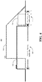
FIG. 4 is a plot of an example of an operating region of a safety assembly according to an embodiment; -
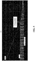
FIG. 5 is a plot of an example of a timer output according to an embodiment; and -
FIGs. 6A and6B are flowcharts of examples of methods of operating a safety assembly according to an embodiment. - Turning now to
FIG. 1 , a plurality of SSDs 10 (10a-10n, e.g., in a storage server) is shown in which first SSD 10a has a safe touch temperature, asecond SSD 10b has an unsafe touch temperature (e.g., has an enclosure temperature that exceeds a threshold such as 70°C and is therefore considered "hot"), and an nth SSD 10n that has a safe touch temperature. In an embodiment, theSSDs 10 include indicators 12 (12a-12n) of whether the respective touch temperatures of theSSDs 10 are safe. For example, afirst indicator 12a is not activated to signify that thefirst SSD 10a has a safe touch temperature, asecond indicator 12b is activated (e.g., flashed, blinked) to signify that thesecond SSD 10b has an unsafe touch temperature, and an nth indicator 12n is not activated to signify that the nth SSD 10n has a safe temperature. Theindicators 12 may be visual notification devices (e.g., light emitting diodes/LEDs). In one example, thesecond indicator 12b is an LED that is flashed (e.g., to emit light pulses) at a certain duty cycle (e.g., 10%) and frequency (e.g., 3Hz) when the enclosure temperature is unsafe. - The illustrated
SSDs 10 are safety-enhanced for several reasons. For example, theindicators 12 may obviate any need for toolbox software, which may retrieve incomplete, inaccurate and/or unreliable temperature readings if temperature reporting firmware or hardware within theSSDs 10 malfunctions (e.g., due to power rail shorts, incorrect calibration). Moreover, theindicators 12 reduce the likelihood that a technician may incorrectly check the temperature of thefirst SSD 10a or the nth SSD 10n and assume that thesecond SSD 10b is safe to touch. Additionally, theindicators 12 may be operable even after the SSDs 10 are powered down, which is a significant advantage over toolbox software. -
FIG. 2 shows anSSD 20 that includes anenclosure 22, a non-volatile memory (NVM)device 24, adevice controller 26 coupled to theNVM device 24, acapacitor 28, abackup voltage line 30 coupled to thecapacitor 28, and asafety assembly 32. In the illustrated example,heat 34 generated by thedevice controller 26 and/orNVM device 24 may reach theenclosure 22. Thesafety assembly 32 may include a temperature comparator 21 (e.g., thermistor) positioned in a location to detect theheat 34 and anindicator 23 positioned in a location that is visible to end users when theSSD 20 is installed. In an embodiment, if theheat 34 causes the temperature of theenclosure 22 to exceed a threshold (e.g., 70°C so that the outer surface becomes unsafe to touch), thesafety assembly 32 outputs light pulses 36 to alert nearby individuals (e.g., technicians) of the unsafe condition. As will be discussed in greater detail, thecapacitor 28 may be charged to a backup voltage (e.g., power loss imminent/PLI voltage) during operation of theSSD 20. Accordingly, the backup voltage may be used to power thesafety assembly 32 when the SSD 20 is powered off (e.g., when traditional toolbox software is unusable to detect the hot and hazardous condition). - Thus, the SSD 20 is safety-enhanced at least to the extent that the
safety assembly 32 obviates any need for toolbox software, which may retrieve incomplete, inaccurate and/or unreliable temperature readings if temperature reporting firmware or hardware within theSSD 20 malfunctions. Moreover, thesafety assembly 32 reduces the likelihood that a technician may incorrectly check the temperature of the wrong SSD (not shown) and assume that theSSD 20 is safe to touch. Additionally, thesafety assembly 32 may be operable even after the SSD 20 is powered down, unlike toolbox software. - The
SSD 20 may be part of a memory device that includes non-volatile memory and/or volatile memory. Non-volatile memory is a storage medium that does not require power to maintain the state of data stored by the medium. In one embodiment, the memory structure is a block addressable storage device, such as those based on NAND or NOR technologies. A storage device may also include future generation nonvolatile devices, such as a three-dimensional (3D) Xpoint memory device, or other byte addressable write-in-place nonvolatile memory devices. In one embodiment, the storage device may be or may include memory devices that use silicon-oxide-nitride-oxide-silicon (SONOS) memory, electrically erasable programmable read-only memory (EEPROM), chalcogenide glass, multi-threshold level NAND flash memory, NOR flash memory, single or multilevel Phase Change Memory (PCM), a resistive memory, nanowire memory, ferroelectric transistor random access memory (FeTRAM), anti-ferroelectric memory, magnetoresistive random access memory (MRAM) memory that incorporates memristor technology, resistive memory including the metal oxide base, the oxygen vacancy base and the conductive bridge Random Access Memory (CB-RAM), or spin transfer torque (STT)-MRAM, a spintronic magnetic junction memory based device, a magnetic tunneling junction (MTJ) based device, a DW (Domain Wall) and SOT (Spin Orbit Transfer) based device, a thiristor based memory device, or a combination of any of the above, or other memory. The term "storage device" may refer to the die itself and/or to a packaged memory product. In some embodiments, 3D Xpoint memory may comprise a transistor-less stackable cross point architecture in which memory cells sit at the intersection of word lines and bit lines and are individually addressable and in which bit storage is based on a change in bulk resistance. In particular embodiments, a memory module with non-volatile memory may comply with one or more standards promulgated by the Joint Electron Device Engineering Council (JEDEC), such as JESD235, JESD218, JESD219, JESD220-1, JESD223B, JESD223-1, or other suitable standard (the JEDEC standards cited herein are available at jedec.org). - Volatile memory is a storage medium that requires power to maintain the state of data stored by the medium. Examples of volatile memory may include various types of random access memory (RAM), such as dynamic random access memory (DRAM) or static random access memory (SRAM). One particular type of DRAM that may be used in a memory module is synchronous dynamic random access memory (SDRAM). In particular embodiments, DRAM of the memory modules complies with a standard promulgated by JEDEC, such as JESD79F for Double Data Rate (DDR) SDRAM, JESD79-2F for DDR2 SDRAM, JESD79-3F for DDR3 SDRAM, or JESD79-4A for DDR4 SDRAM (these standards are available at jedec.org). Such standards (and similar standards) may be referred to as DDR-based standards and communication interfaces of the storage devices that implement such standards may be referred to as DDR-based interfaces.
- Turning now to
FIG. 3A , asafety assembly 40 is shown in which atimer circuit 42 includes an input node 44 (e.g., contact, pin, trace, connection) coupled to abackup voltage line 46, areset node 48, and anoutput node 50. Thesafety assembly 40 may also include anindicator circuit 52 coupled to theoutput node 50 of thetimer circuit 42. In an embodiment, atemperature comparator circuit 54 is coupled to thereset node 48 of thetimer circuit 42, wherein if an enclosure temperature (e.g., surface temperature of an SSD enclosure) exceeds a threshold while a backup voltage (e.g., PLI voltage) is present on thebackup voltage line 46, thetemperature comparator circuit 54 causes thetimer circuit 42 to trigger light pulses from theindicator circuit 52. - In one example, the
timer circuit 42 includes a regulator 56 (e.g., low dropout/LDO or buck-boost regulator) including theinput node 44, aregulator output node 58, and anenablement node 60. Additionally, thetimer circuit 42 may include a timer device 62 (e.g., 555 timer integrated circuit/IC) having theoutput node 50, thereset node 48, and atimer input node 64 coupled to theregulator output node 58. Theregulator 56 may convert the backup voltage (e.g., 35V) down to an operating voltage voltage (e.g., Vcc of 3.3V) that is provided to thetimer device 62 via a step-down voltage line 76. In an embodiment, theenablement node 60 is coupled to amain voltage line 66. Thus, a lack of a main voltage (Vmain) on the main voltage line 66 (e.g., system power is off) enables thetimer circuit 42 and the light pulses. By contrast, a presence of the main voltage on themain voltage line 66 disables thetimer circuit 42 and the light pulses. Accordingly, the illustratedsafety assembly 40 operates only when system power is off and while the backup voltage is present on thebackup voltage line 46. As will be discussed in greater detail, the backup voltage may be provided by a capacitor 68 (e.g., aluminum electrolytic capacitor), which will discharge during operation of thesafety assembly 40. Proper selection of the operating parameters of thetimer device 62 may ensure that the light pulses are generated long enough for the enclosure temperature to fall below the safety threshold. - The illustrated
temperature comparator circuit 54 includes a temperature comparator device 70 (e.g., thermistor positioned adjacent to the enclosure and/or heat-generating components) coupled to a ground connection 72 (e.g., contact, pin, trace, node) and thereset node 48. Additionally, thetemperature comparator circuit 54 may include adivider resistor 74 coupled to thereset node 48 and the step-down voltage line 76 (VLDO) of thetimer circuit 42. In an embodiment, theindicator circuit 52 includes a switch 78 (e.g., metal oxide semiconductor field effect transistor/MOSFET) coupled to theoutput node 50 and theground connection 72. In one example, anLED 80 is coupled to theswitch 78 and aseries resistor 82 is coupled to theLED 80 and the step-downvoltage line 76 of thetimer circuit 76. TheLED 80 may be mounted in a position that is visible through the enclosure while the SSD is installed in a system such as, for example, a data storage server. Indeed, theLED 80 may be a standard component in EDSFF (Enterprise and Data Center SSD Form Factor) SSDs. - During operation, when enclosure temperature exceeds the threshold, the
temperature comparator device 70 will transition to a high resistance or open state and activate thetimer device 62 by pulling thereset node 48 high. Activating thetimer device 62 causes theoutput node 50 to periodically activate theLED 80 via theswitch 78. As already noted, theindicator circuit 52 may be modified to include a speaker/buzzer instead of, or in addition to, theLED 80 to provide audible/sound notifications. -
FIG. 3B shows asafety assembly 90 that is the same as the safety assembly 40 (FIG. 3A ) except that theenablement node 60 is coupled to theground connection 72. Accordingly, theground connection 72 enables thetimer circuit 42 and the light pulses while when the system power is both powered off and powered on. In the illustrated solution, theLED 80 may be an additional LED that is dedicated to the safety assembly 90 (e.g., not shared with other components of the SSD). -
FIG. 4 shows aplot 100 of a main voltage (Vmain)curve 102, a backup voltage (VPLI)curve 104, and a step-down voltage curve 106 (VLDO). In the illustrated example, the safety assembly is not operating during aperiod 108 when the main voltage is present. At time to, the main voltage is turned off, the step-down voltage goes high, the backup voltage begins to drop (e.g., due to discharge of the PLI capacitor), and aperiod 110 begins. At time ti, the backup voltage reaches the step-down voltage and the step-down voltage begins to drop along with the backup voltage. At time t2, the safety assembly ceases operation. In an embodiment, operating parameters such as the duty cycle and frequency of the LED are selected so that theperiod 110 is long enough for the enclosure to cool down to a safe temperature. - For example,
FIG. 5 demonstrates in aplot 120 that with a 2000uF aluminum electrolytic capacitor charged to 20V, a 10% duty cycle and a blinking frequency of 3Hz, the safety assembly 40 (FIG. 3A ) can operate for up to 55 seconds. A capacitor voltage value of 20V is chosen as empirical data shows that firmware can complete a PLI data dump before the PLI voltage drops below 20V from a full charge of 35V. A duty cycle value of 10% may minimize the energy needed to blink/flash the LED. Additionally, an SSD having an E1.L form factor may have 100 seconds to cool down from 70°C to 50°C. The operating duration of the safety assembly may be further extended using techniques such as increasing the PLI capacitor capacitance, increasing the PLI voltage, using a buck-boost regulator, which will generate output voltages at lower input voltages and with better efficiency, and so forth. -
FIG. 6A shows amethod 130 of operating a performance-enhanced safety assembly. Themethod 130 may generally be implemented in a safety assembly such as, for example, the safety assembly 40 (FIG. 3A ), already discussed. More particularly, themethod 130 may be implemented in configurable logic such as, for example, programmable logic arrays (PLAs), field-programmable gate arrays (FPGAs), complex programmable logic devices (CPLDs), in fixed-functionality hardware logic using circuit technology such as, for example, application-specific integrated circuit (ASIC), complementary metal oxide semiconductor (CMOS) or transistor-transistor logic (TTL) technology, or any combination thereof. - Illustrated
processing block 132 determines whether a main voltage is present on a main voltage line. If not, block 134 enables, via a lack of the main voltage on the main voltage line, a timer circuit and light pulses. In an embodiment, block 136 causes, by a temperature comparator circuit, the timer circuit to trigger the light pulses from an indicator circuit if an enclosure temperature exceeds a threshold while a backup voltage is present on a backup voltage line. In the illustrated example, the timer circuit includes an input node coupled to the backup voltage line, a reset node (e.g., input of the timer circuit), and an output node. Additionally, the indicator circuit may be coupled to the output node of the timer circuit and the temperature comparator circuit may be coupled to the reset node of the timer circuit. In one example, the timer circuit includes a regulator including the input node, a regulator output node, and an enablement node and a timer device including the output node, the reset node, and a timer input node coupled to the regulator output node. In an embodiment, the enablement node is coupled to the main voltage line. If it is determined atblock 132 that the main voltage is present on the main voltage line, block 138 disables, via the presence of the main voltage on the main voltage line, the timer circuit and the light pulses. - The
method 130 therefore enhances performance and safety at least to the extent that the safety assembly obviates any need for toolbox software, which may retrieve incomplete, inaccurate and/or unreliable temperature readings if temperature reporting firmware or hardware within the SSD malfunctions. Moreover, themethod 130 reduces the likelihood that a technician may incorrectly check the temperature of the wrong SSD and assume that the hot and hazardous SSD is safe to touch. Additionally, themethod 130 is operable even after the SSD is powered off, unlike toolbox software. -
FIG. 6B shows anothermethod 140 of operating a performance-enhanced safety assembly. Themethod 140 may generally be implemented in a safety assembly such as, for example, safety assembly 90 (FIG. 3B ), already discussed. More particularly, themethod 140 may be implemented in configurable logic such as, for example, PLAs, FPGAs, CPLDs, in fixed-functionality hardware logic using circuit technology such as, for example, ASIC, CMOS or TTL technology, or any combination thereof. - Illustrated
processing block 142 enables, via a ground connection, a timer circuit and light pulses. In an embodiment, block 144 causes, by a temperature comparator circuit, the timer circuit to trigger the light pulses from an indicator circuit if an enclosure temperature exceeds a threshold while a backup voltage is present on a backup voltage line. In the illustrated example, the timer circuit includes an input node coupled to the backup voltage line, a reset node (e.g., input of the timer circuit), and an output node. Additionally, the indicator circuit may be coupled to the output node of the timer circuit and the temperature comparator circuit may be coupled to the reset node of the timer circuit. In one example, the timer circuit includes a regulator including the input node, a regulator output node, and an enablement node and a timer device including the output node, the reset node, and a timer input node coupled to the regulator output node. In an embodiment, the enablement node is coupled to the ground connection. - The
method 140 therefore enhances performance and safety at least to the extent that the safety assembly obviates any need for toolbox software, which may retrieve incomplete, inaccurate and/or unreliable temperature readings if temperature reporting firmware or hardware within the SSD malfunctions. Moreover, themethod 140 reduces the likelihood that a technician may incorrectly check the temperature of the wrong SSD and assume that the hot and hazardous SSD is safe to touch. Additionally, themethod 130 is operable when the SSD is both powered on and powered off, unlike toolbox software. -
- Example 1 includes a performance-enhanced solid state drive (SSD) comprising an enclosure, a non-volatile memory (NVM) device, a device controller coupled the NVM device, a capacitor, a backup voltage line coupled to the capacitor, and a safety assembly comprising a timer circuit including an input node coupled to the backup voltage line, a reset node, and an output node, an indicator circuit coupled to the output node of the timer circuit, and a temperature comparator circuit coupled to the reset node of the timer circuit, wherein if a temperature of the enclosure exceeds a threshold while a backup voltage is present on the backup voltage line, the temperature comparator circuit causes the timer circuit to trigger light pulses from the indicator circuit.
- Example 2 includes the SSD of Example 1, wherein the timer circuit includes a regulator including the input node, a regulator output node, and an enablement node, and a timer device including the output node, the reset node, and a timer input node coupled to the regulator output node.
- Example 3 includes the SSD of Example 2, wherein the enablement node is coupled to a main voltage line, wherein a lack of a main voltage on the main voltage line enables the timer circuit and the light pulses while the SSD is powered off, and wherein a presence of main voltage on the main voltage line disables the light pulses and the light pulses while the SSD is powered on.
- Example 4 includes the SSD of Example 2, wherein the enablement node is coupled to a ground connection, and wherein the ground connection enables the timer circuit and the light pulses while the SSD is powered on and powered off.
- Example 5 includes the SSD of Example 2, wherein the regular includes a low dropout regulator.
- Example 6 includes the SSD of Example 2, wherein the regular includes a buck-boost regulator.
- Example 7 includes the SSD of Example 1, wherein the temperature comparator circuit includes a temperature comparator device coupled to a ground connection and the reset node, and a divider resistor coupled to the reset node and a step-down voltage line of the timer circuit.
- Example 8 includes the SSD of any one of Examples 1 to 7, wherein the indicator circuit includes a switch coupled to the output node and a ground connection, a light emitting diode (LED) coupled to the switch, and a series resistor coupled to the LED and a step-down voltage line of the timer circuit.
- Example 9 includes a performance-enhanced safety assembly comprising a timer circuit including an input node coupled to a backup voltage line, a reset node, and an output node, an indicator circuit coupled to the output node of the timer circuit, and a temperature comparator circuit coupled to the reset node of the timer circuit, wherein if an enclosure temperature exceeds a threshold while a backup voltage is present on the backup voltage line, the temperature comparator circuit causes the timer circuit to trigger light pulses from the indicator circuit.
- Example 10 includes the safety assembly of Example 9, wherein the timer circuit includes a regulator including the input node, a regulator output node, and an enablement node, and a timer device including the output node, the reset node, and a timer input node coupled to the regulator output node.
- Example 11 includes the safety assembly of Example 10, wherein the enablement node is coupled to a main voltage line, wherein a lack of a main voltage on the main voltage line enables the timer circuit and the light pulses, and wherein a presence of main voltage on the main voltage line disables the timer circuit and the light pulses.
- Example 12 includes the safety assembly of Example 10, wherein the enablement node is coupled to a ground connection, and wherein the ground connection enables the timer circuit and the light pulses.
- Example 13 includes the safety assembly of Example 10, wherein the regular includes a low dropout regulator.
- Example 14 includes the safety assembly of Example 10, wherein the regular includes a buck-boost regulator.
- Example 15 includes the safety assembly of Example 9, wherein the temperature comparator circuit includes a temperature comparator device coupled to a ground connection and the reset node, and a divider resistor coupled to the reset node and a step-down voltage line of the timer circuit.
- Example 16 includes the safety assembly of any one of Examples 9 to 15, wherein the indicator circuit includes a switch coupled to the output node and a ground connection, a light emitting diode (LED) coupled to the switch, and a series resistor coupled to the LED and a step-down voltage line of the timer circuit.
- Example 17 includes a method of operating a safety assembly, the method comprising causing, by a temperature comparator circuit, a timer circuit to trigger light pulses from an indicator circuit if an enclosure temperature exceeds a threshold while a backup voltage is present on a backup voltage line, wherein the timer circuit includes an input node coupled to the backup voltage line, a reset node, and an output node, wherein the indicator circuit is coupled to the output node of the timer circuit, and wherein the temperature comparator circuit is coupled to the reset node of the timer circuit.
- Example 18 includes the method of Example 17, wherein the timer circuit includes a regulator including the input node, a regulator output node, and an enablement node and a timer device including the output node, the reset node, and a timer input node coupled to the regulator output node, wherein the enablement node is coupled to a main voltage line, and wherein the method further includes enabling, via a lack of a main voltage on the main voltage line, the timer circuit and the light pulses, and disabling, via a presence of main voltage on the main voltage line, the timer circuit and the light pulses.
- Example 19 includes the method of Example 17, wherein the timer circuit includes a regulator including the input node, a regulator output node, and an enablement node and a timer device including the output node, the reset node, and a timer input node coupled to the regulator output node, wherein the enablement node is coupled to a ground connection, and wherein the method further includes enabling, via the ground connection, the timer circuit and the light pulses.
- Technology described herein therefore provides a visible indicator (e.g., located on the front of a drive to be user visible) of the drive running hot. The technology is firmware and software independent and it may operate even if firmware is not executing due to a severe failure. The technology also reduces the possibility of injuries due to human error reading the wrong SSD enclosure temperature from an SSD toolbox. Additionally, the technology provides an alternative to thermal throttling, which may reduce performance or require additional airflow or heat pipe components to maintain performance (e.g., leading to increased cost and a lack of competitiveness). Moreover, the technology enhances safety over regulatory warning labels that are not visible to the user when the SSD is assembled in the system.
- Embodiments are applicable for use with all types of semiconductor integrated circuit ("IC") chips. Examples of these IC chips include but are not limited to processors, controllers, chipset components, programmable logic arrays (PLAs), memory chips, network chips, systems on chip (SoCs), SSD/NAND controller ASICs, and the like. In addition, in some of the drawings, signal conductor lines are represented with lines. Some may be different, to indicate more constituent signal paths, have a number label, to indicate a number of constituent signal paths, and/or have arrows at one or more ends, to indicate primary information flow direction. This, however, should not be construed in a limiting manner. Rather, such added detail may be used in connection with one or more exemplary embodiments to facilitate easier understanding of a circuit. Any represented signal lines, whether or not having additional information, may actually comprise one or more signals that may travel in multiple directions and may be implemented with any suitable type of signal scheme, e.g., digital or analog lines implemented with differential pairs, optical fiber lines, and/or single-ended lines.
- Example sizes/models/values/ranges may have been given, although embodiments are not limited to the same. As manufacturing techniques (e.g., photolithography) mature over time, it is expected that devices of smaller size could be manufactured. In addition, well known power/ground connections to IC chips and other components may or may not be shown within the figures, for simplicity of illustration and discussion, and so as not to obscure certain aspects of the embodiments. Further, arrangements may be shown in block diagram form in order to avoid obscuring embodiments, and also in view of the fact that specifics with respect to implementation of such block diagram arrangements are highly dependent upon the platform within which the embodiment is to be implemented, i.e., such specifics should be well within purview of one skilled in the art. Where specific details (e.g., circuits) are set forth in order to describe example embodiments, it should be apparent to one skilled in the art that embodiments can be practiced without, or with variation of, these specific details. The description is thus to be regarded as illustrative instead of limiting.
- The term "coupled" may be used herein to refer to any type of relationship, direct or indirect, between the components in question, and may apply to electrical, mechanical, fluid, optical, electromagnetic, electromechanical or other connections. In addition, the terms "first", "second", etc. may be used herein only to facilitate discussion, and carry no particular temporal or chronological significance unless otherwise indicated.
- As used in this application and in the claims, a list of items joined by the term "one or more of' may mean any combination of the listed terms. For example, the phrases "one or more of A, B or C" may mean A; B; C; A and B; A and C; B and C; or A, B and C.
- Those skilled in the art will appreciate from the foregoing description that the broad techniques of the embodiments can be implemented in a variety of forms. Therefore, while the embodiments have been described in connection with particular examples thereof, the true scope of the embodiments should not be so limited since other modifications will become apparent to the skilled practitioner upon a study of the drawings, specification, and following claims.
Claims (15)
- A solid state drive (SSD) comprising:an enclosure;a non-volatile memory (NVM) device;a device controller coupled to the NVM device;a capacitor;a backup voltage line coupled to the capacitor; anda safety assembly comprising:a timer circuit including an input node coupled to the backup voltage line, a reset node, and an output node,an indicator circuit coupled to the output node of the timer circuit, anda temperature comparator circuit coupled to the reset node of the timer circuit, wherein if a temperature of the enclosure exceeds a threshold while a backup voltage is present on the backup voltage line, the temperature comparator circuit causes the timer circuit to trigger light pulses from the indicator circuit.
- The SSD of claim 1, wherein the timer circuit includes:a regulator including the input node, a regulator output node, and an enablement node, anda timer device including the output node, the reset node, and a timer input node coupled to the regulator output node.
- The SSD of claim 2, wherein the enablement node is coupled to a main voltage line, wherein a lack of a main voltage on the main voltage line enables the timer circuit and the light pulses while the SSD is powered off, and wherein a presence of main voltage on the main voltage line disables the light pulses and the light pulses while the SSD is powered on.
- The SSD of claim 2 or 3, wherein the enablement node is coupled to a ground connection, and wherein the ground connection enables the timer circuit and the light pulses while the SSD is powered on and powered off.
- The SSD of claim 2, 3 or 4, wherein the regular includes a low dropout regulator.
- The SSD of claim 2, 3 4 or 5, wherein the regular includes a buck-boost regulator.
- The SSD of one of the previous claims, wherein the temperature comparator circuit includes:a temperature comparator device coupled to a ground connection and the reset node, anda divider resistor coupled to the reset node and a step-down voltage line of the timer circuit.
- The SSD of one of the previous claims, wherein the indicator circuit includes:a switch coupled to the output node and a ground connection,a light emitting diode (LED) coupled to the switch, anda series resistor coupled to the LED and a step-down voltage line of the timer circuit.
- A safety assembly comprising:a timer circuit including an input node coupled to a backup voltage line, a reset node, and an output node;an indicator circuit coupled to the output node of the timer circuit; anda temperature comparator circuit coupled to the reset node of the timer circuit, wherein if an enclosure temperature exceeds a threshold while a backup voltage is present on the backup voltage line, the temperature comparator circuit causes the timer circuit to trigger light pulses from the indicator circuit.
- The safety assembly of claim 9, wherein the timer circuit includes:a regulator including the input node, a regulator output node, and an enablement node; anda timer device including the output node, the reset node, and a timer input node coupled to the regulator output node.
- The safety assembly of claim 10, wherein the enablement node is coupled to a main voltage line, wherein a lack of a main voltage on the main voltage line enables the timer circuit and the light pulses, and wherein a presence of main voltage on the main voltage line disables the timer circuit and the light pulses.
- A method of operating a safety assembly, the method comprising:
causing, by a temperature comparator circuit, a timer circuit to trigger light pulses from an indicator circuit if an enclosure temperature exceeds a threshold while a backup voltage is present on a backup voltage line, wherein the timer circuit includes an input node coupled to the backup voltage line, a reset node, and an output node, wherein the indicator circuit is coupled to the output node of the timer circuit, and wherein the temperature comparator circuit is coupled to the reset node of the timer circuit. - The method of claim 12, wherein the timer circuit includes a regulator including the input node, a regulator output node, and an enablement node and a timer device including the output node, the reset node, and a timer input node coupled to the regulator output node, wherein the enablement node is coupled to a main voltage line, and wherein the method further includes:enabling, via a lack of a main voltage on the main voltage line, the timer circuit and the light pulses; anddisabling, via a presence of main voltage on the main voltage line, the timer circuit and the light pulses.
- The method of claim 12 or 13, wherein the timer circuit includes a regulator including the input node, a regulator output node, and an enablement node and a timer device including the output node, the reset node, and a timer input node coupled to the regulator output node, wherein the enablement node is coupled to a ground connection, and wherein the method further includes enabling, via the ground connection, the timer circuit and the light pulses.
- An apparatus, comprising:
means for performing the methods according to any one of claims 12-14.
Applications Claiming Priority (1)
| Application Number | Priority Date | Filing Date | Title |
|---|---|---|---|
| US17/313,603 US12119638B2 (en) | 2021-05-06 | 2021-05-06 | Hot and hazardous indicator on solid state drives |
Publications (4)
| Publication Number | Publication Date |
|---|---|
| EP4086907A1 true EP4086907A1 (en) | 2022-11-09 |
| EP4086907B1 EP4086907B1 (en) | 2026-01-07 |
| EP4086907C0 EP4086907C0 (en) | 2026-01-07 |
| EP4086907B8 EP4086907B8 (en) | 2026-02-25 |
Family
ID=77273596
Family Applications (1)
| Application Number | Title | Priority Date | Filing Date |
|---|---|---|---|
| EP22165655.6A Active EP4086907B8 (en) | 2021-05-06 | 2022-03-30 | Hot and hazardous indicator on solid state drives |
Country Status (3)
| Country | Link |
|---|---|
| US (1) | US12119638B2 (en) |
| EP (1) | EP4086907B8 (en) |
| CN (1) | CN115312088A (en) |
Cited By (1)
| Publication number | Priority date | Publication date | Assignee | Title |
|---|---|---|---|---|
| TWI918019B (en) | 2023-07-19 | 2026-03-11 | 大陸商長江存儲科技有限責任公司 | Power loss protection and reset signal generation in memory systems |
Citations (3)
| Publication number | Priority date | Publication date | Assignee | Title |
|---|---|---|---|---|
| DE102008054603A1 (en) * | 2008-12-14 | 2010-06-24 | Getac Technology Corp. | Hard disk temperature rise protection device for monitoring computer-internal hard disk temperatures, has data exchange-filter module for providing access to hard disk when temperature of hard disk reaches preset value |
| US20110140898A1 (en) * | 2009-12-10 | 2011-06-16 | Dell Products L.P. | System and Method for Visually Indicating Unsafe Handling Temperature of an Information Handling System Component |
| US20130120149A1 (en) * | 2009-10-19 | 2013-05-16 | Stuart Allen Berke | System and method for safe handling of information handling resources |
Family Cites Families (3)
| Publication number | Priority date | Publication date | Assignee | Title |
|---|---|---|---|---|
| US10362715B2 (en) * | 2015-10-13 | 2019-07-23 | Lenovo Enterprise Solutions (Singapore) Pte. Ltd. | Automatically cooling computer system components for safe servicing |
| JP7372767B2 (en) * | 2019-06-25 | 2023-11-01 | ローム株式会社 | Power circuit, power cut-off protection controller, data storage device |
| US11861186B2 (en) * | 2021-04-10 | 2024-01-02 | Innogrit Technologies Co., Ltd. | System and method for managing solid state storage devices in low temperature environment |
-
2021
- 2021-05-06 US US17/313,603 patent/US12119638B2/en active Active
-
2022
- 2022-03-30 EP EP22165655.6A patent/EP4086907B8/en active Active
- 2022-04-06 CN CN202210368449.8A patent/CN115312088A/en active Pending
Patent Citations (3)
| Publication number | Priority date | Publication date | Assignee | Title |
|---|---|---|---|---|
| DE102008054603A1 (en) * | 2008-12-14 | 2010-06-24 | Getac Technology Corp. | Hard disk temperature rise protection device for monitoring computer-internal hard disk temperatures, has data exchange-filter module for providing access to hard disk when temperature of hard disk reaches preset value |
| US20130120149A1 (en) * | 2009-10-19 | 2013-05-16 | Stuart Allen Berke | System and method for safe handling of information handling resources |
| US20110140898A1 (en) * | 2009-12-10 | 2011-06-16 | Dell Products L.P. | System and Method for Visually Indicating Unsafe Handling Temperature of an Information Handling System Component |
Cited By (1)
| Publication number | Priority date | Publication date | Assignee | Title |
|---|---|---|---|---|
| TWI918019B (en) | 2023-07-19 | 2026-03-11 | 大陸商長江存儲科技有限責任公司 | Power loss protection and reset signal generation in memory systems |
Also Published As
| Publication number | Publication date |
|---|---|
| US12119638B2 (en) | 2024-10-15 |
| EP4086907B8 (en) | 2026-02-25 |
| EP4086907B1 (en) | 2026-01-07 |
| US20210257828A1 (en) | 2021-08-19 |
| EP4086907C0 (en) | 2026-01-07 |
| CN115312088A (en) | 2022-11-08 |
Similar Documents
| Publication | Publication Date | Title |
|---|---|---|
| US9880901B2 (en) | Serial bus DRAM error correction event notification | |
| JP6209646B2 (en) | Nonvolatile memory data management method and system | |
| EP3706126A1 (en) | Techniques to mitigate selection failure for a memory device | |
| TWI754871B (en) | Memory system and power circuit | |
| KR20170028096A (en) | Method for inspecting auxiliary power supply and electronic device adopting the same | |
| CN104112478A (en) | Integrated circuit and memory device | |
| US20140362650A1 (en) | Apparatuses and methods for efficient write in a cross-point array | |
| US12602098B2 (en) | Electronic circuit for outputting voltage based on a plurality of input voltages | |
| US8503247B2 (en) | Semiconductor storage apparatus, and method and system for boosting word lines | |
| US20150102668A1 (en) | Auxiliary power supply devices and electronic systems employing the same | |
| KR101212747B1 (en) | Current Controlling Apparatus And Phase Change Memory Having The Same | |
| CN1959846B (en) | Random access memory, boosting charge pump and method of generating write driving voltage | |
| US12119638B2 (en) | Hot and hazardous indicator on solid state drives | |
| US20170126003A1 (en) | Multi-level output circuit having centralized esd protection | |
| US9887691B2 (en) | Periodic signal generation circuit and semiconductor system including the same | |
| US12626733B2 (en) | Power management integrated circuit and memory module including the same | |
| CN106409246A (en) | Dc-dc converter and driving method thereof | |
| US9472279B2 (en) | Memory cell dynamic grouping using write detection | |
| CN105280216B (en) | Semiconductor memory device and method of operating the same | |
| US8013753B2 (en) | Method for detecting operations of a power storage device and related power storage device | |
| US9466366B1 (en) | Resistive memory and memory cell thereof | |
| JP5668519B2 (en) | Write control circuit and semiconductor device | |
| KR20260023625A (en) | Method and device for operating a memory system | |
| CN104182023A (en) | Power supply circuit | |
| CN101713805A (en) | Method for detecting operation condition of power storage device and power storage device thereof |
Legal Events
| Date | Code | Title | Description |
|---|---|---|---|
| PUAI | Public reference made under article 153(3) epc to a published international application that has entered the european phase |
Free format text: ORIGINAL CODE: 0009012 |
|
| STAA | Information on the status of an ep patent application or granted ep patent |
Free format text: STATUS: THE APPLICATION HAS BEEN PUBLISHED |
|
| AK | Designated contracting states |
Kind code of ref document: A1 Designated state(s): AL AT BE BG CH CY CZ DE DK EE ES FI FR GB GR HR HU IE IS IT LI LT LU LV MC MK MT NL NO PL PT RO RS SE SI SK SM TR |
|
| STAA | Information on the status of an ep patent application or granted ep patent |
Free format text: STATUS: REQUEST FOR EXAMINATION WAS MADE |
|
| 17P | Request for examination filed |
Effective date: 20230509 |
|
| RBV | Designated contracting states (corrected) |
Designated state(s): AL AT BE BG CH CY CZ DE DK EE ES FI FR GB GR HR HU IE IS IT LI LT LU LV MC MK MT NL NO PL PT RO RS SE SI SK SM TR |
|
| RIC1 | Information provided on ipc code assigned before grant |
Ipc: G11C 7/04 20060101AFI20250625BHEP Ipc: G11C 7/24 20060101ALI20250625BHEP Ipc: G11C 16/22 20060101ALI20250625BHEP Ipc: G11C 16/30 20060101ALI20250625BHEP Ipc: G11C 16/32 20060101ALI20250625BHEP Ipc: G11C 5/14 20060101ALI20250625BHEP Ipc: G06F 1/20 20060101ALI20250625BHEP Ipc: G06F 11/14 20060101ALI20250625BHEP Ipc: G06F 11/30 20060101ALI20250625BHEP Ipc: G06F 11/32 20060101ALI20250625BHEP Ipc: H02H 5/04 20060101ALI20250625BHEP Ipc: H05B 45/00 20220101ALI20250625BHEP Ipc: G06F 1/30 20060101ALI20250625BHEP Ipc: G06F 11/20 20060101ALI20250625BHEP |
|
| GRAP | Despatch of communication of intention to grant a patent |
Free format text: ORIGINAL CODE: EPIDOSNIGR1 |
|
| STAA | Information on the status of an ep patent application or granted ep patent |
Free format text: STATUS: GRANT OF PATENT IS INTENDED |
|
| INTG | Intention to grant announced |
Effective date: 20250801 |
|
| RIN1 | Information on inventor provided before grant (corrected) |
Inventor name: CHAY, CHIN FATT Inventor name: MORNING-SMITH, ANDREW Inventor name: KHOO, BOON SEONG Inventor name: ROTHMAN, TIMOTHY Inventor name: KHOR, YI HENG |
|
| GRAS | Grant fee paid |
Free format text: ORIGINAL CODE: EPIDOSNIGR3 |
|
| GRAA | (expected) grant |
Free format text: ORIGINAL CODE: 0009210 |
|
| STAA | Information on the status of an ep patent application or granted ep patent |
Free format text: STATUS: THE PATENT HAS BEEN GRANTED |
|
| AK | Designated contracting states |
Kind code of ref document: B1 Designated state(s): AL AT BE BG CH CY CZ DE DK EE ES FI FR GB GR HR HU IE IS IT LI LT LU LV MC MK MT NL NO PL PT RO RS SE SI SK SM TR |
|
| REG | Reference to a national code |
Ref country code: CH Ref legal event code: F10 Free format text: ST27 STATUS EVENT CODE: U-0-0-F10-F00 (AS PROVIDED BY THE NATIONAL OFFICE) Effective date: 20260107 Ref country code: GB Ref legal event code: FG4D |
|
| REG | Reference to a national code |
Ref country code: DE Ref legal event code: R096 Ref document number: 602022028249 Country of ref document: DE |
|
| REG | Reference to a national code |
Ref country code: DE Ref legal event code: R081 Ref document number: 602022028249 Country of ref document: DE Owner name: SK HYNIX NAND PRODUCT SOLUTIONS CORP., RANCHO , US Free format text: FORMER OWNER: INTEL CORPORATION, SANTA CLARA, CA, US |
|
| REG | Reference to a national code |
Ref country code: CH Ref legal event code: Q17 Free format text: ST27 STATUS EVENT CODE: U-0-0-Q10-Q17 (AS PROVIDED BY THE NATIONAL OFFICE) Effective date: 20260128 Ref country code: CH Ref legal event code: W10 Free format text: ST27 STATUS EVENT CODE: U-0-0-W10-W00 (AS PROVIDED BY THE NATIONAL OFFICE) Effective date: 20260128 Ref country code: IE Ref legal event code: FG4D |
|
| RAP2 | Party data changed (patent owner data changed or rights of a patent transferred) |
Owner name: SK HYNIX NAND PRODUCT SOLUTIONS CORP. |
|
| U01 | Request for unitary effect filed |
Effective date: 20260205 |
|
| U07 | Unitary effect registered |
Designated state(s): AT BE BG DE DK EE FI FR IT LT LU LV MT NL PT RO SE SI Effective date: 20260211 |
|
| PGFP | Annual fee paid to national office [announced via postgrant information from national office to epo] |
Ref country code: AT Payment date: 20260301 Year of fee payment: 5 |
|
| U20 | Renewal fee for the european patent with unitary effect paid |
Year of fee payment: 5 Effective date: 20260331 |