EP4085222B1 - Device housing with lighting - Google Patents
Device housing with lighting Download PDFInfo
- Publication number
- EP4085222B1 EP4085222B1 EP20851268.1A EP20851268A EP4085222B1 EP 4085222 B1 EP4085222 B1 EP 4085222B1 EP 20851268 A EP20851268 A EP 20851268A EP 4085222 B1 EP4085222 B1 EP 4085222B1
- Authority
- EP
- European Patent Office
- Prior art keywords
- light
- leds
- device housing
- light pipe
- housing
- Prior art date
- Legal status (The legal status is an assumption and is not a legal conclusion. Google has not performed a legal analysis and makes no representation as to the accuracy of the status listed.)
- Active
Links
Images






Classifications
-
- F—MECHANICAL ENGINEERING; LIGHTING; HEATING; WEAPONS; BLASTING
- F21—LIGHTING
- F21V—FUNCTIONAL FEATURES OR DETAILS OF LIGHTING DEVICES OR SYSTEMS THEREOF; STRUCTURAL COMBINATIONS OF LIGHTING DEVICES WITH OTHER ARTICLES, NOT OTHERWISE PROVIDED FOR
- F21V5/00—Refractors for light sources
- F21V5/08—Refractors for light sources producing an asymmetric light distribution
-
- G—PHYSICS
- G02—OPTICS
- G02B—OPTICAL ELEMENTS, SYSTEMS OR APPARATUS
- G02B6/00—Light guides; Structural details of arrangements comprising light guides and other optical elements, e.g. couplings
- G02B6/0001—Light guides; Structural details of arrangements comprising light guides and other optical elements, e.g. couplings specially adapted for lighting devices or systems
- G02B6/0005—Light guides; Structural details of arrangements comprising light guides and other optical elements, e.g. couplings specially adapted for lighting devices or systems the light guides being of the fibre type
- G02B6/0006—Coupling light into the fibre
-
- F—MECHANICAL ENGINEERING; LIGHTING; HEATING; WEAPONS; BLASTING
- F21—LIGHTING
- F21V—FUNCTIONAL FEATURES OR DETAILS OF LIGHTING DEVICES OR SYSTEMS THEREOF; STRUCTURAL COMBINATIONS OF LIGHTING DEVICES WITH OTHER ARTICLES, NOT OTHERWISE PROVIDED FOR
- F21V14/00—Controlling the distribution of the light emitted by adjustment of elements
- F21V14/006—Controlling the distribution of the light emitted by adjustment of elements by means of optical elements, e.g. films, filters or screens, being rolled up around a roller
-
- F—MECHANICAL ENGINEERING; LIGHTING; HEATING; WEAPONS; BLASTING
- F21—LIGHTING
- F21V—FUNCTIONAL FEATURES OR DETAILS OF LIGHTING DEVICES OR SYSTEMS THEREOF; STRUCTURAL COMBINATIONS OF LIGHTING DEVICES WITH OTHER ARTICLES, NOT OTHERWISE PROVIDED FOR
- F21V15/00—Protecting lighting devices from damage
- F21V15/01—Housings, e.g. material or assembling of housing parts
-
- F—MECHANICAL ENGINEERING; LIGHTING; HEATING; WEAPONS; BLASTING
- F21—LIGHTING
- F21V—FUNCTIONAL FEATURES OR DETAILS OF LIGHTING DEVICES OR SYSTEMS THEREOF; STRUCTURAL COMBINATIONS OF LIGHTING DEVICES WITH OTHER ARTICLES, NOT OTHERWISE PROVIDED FOR
- F21V3/00—Globes; Bowls; Cover glasses
-
- F—MECHANICAL ENGINEERING; LIGHTING; HEATING; WEAPONS; BLASTING
- F21—LIGHTING
- F21V—FUNCTIONAL FEATURES OR DETAILS OF LIGHTING DEVICES OR SYSTEMS THEREOF; STRUCTURAL COMBINATIONS OF LIGHTING DEVICES WITH OTHER ARTICLES, NOT OTHERWISE PROVIDED FOR
- F21V5/00—Refractors for light sources
- F21V5/02—Refractors for light sources of prismatic shape
-
- G—PHYSICS
- G01—MEASURING; TESTING
- G01N—INVESTIGATING OR ANALYSING MATERIALS BY DETERMINING THEIR CHEMICAL OR PHYSICAL PROPERTIES
- G01N35/00—Automatic analysis not limited to methods or materials provided for in any single one of groups G01N1/00 - G01N33/00; Handling materials therefor
- G01N35/00584—Control arrangements for automatic analysers
-
- G—PHYSICS
- G02—OPTICS
- G02B—OPTICAL ELEMENTS, SYSTEMS OR APPARATUS
- G02B5/00—Optical elements other than lenses
- G02B5/02—Diffusing elements; Afocal elements
- G02B5/0205—Diffusing elements; Afocal elements characterised by the diffusing properties
- G02B5/021—Diffusing elements; Afocal elements characterised by the diffusing properties the diffusion taking place at the element's surface, e.g. by means of surface roughening or microprismatic structures
-
- G—PHYSICS
- G02—OPTICS
- G02B—OPTICAL ELEMENTS, SYSTEMS OR APPARATUS
- G02B5/00—Optical elements other than lenses
- G02B5/02—Diffusing elements; Afocal elements
- G02B5/0205—Diffusing elements; Afocal elements characterised by the diffusing properties
- G02B5/0252—Diffusing elements; Afocal elements characterised by the diffusing properties using holographic or diffractive means
-
- G—PHYSICS
- G02—OPTICS
- G02B—OPTICAL ELEMENTS, SYSTEMS OR APPARATUS
- G02B6/00—Light guides; Structural details of arrangements comprising light guides and other optical elements, e.g. couplings
- G02B6/0001—Light guides; Structural details of arrangements comprising light guides and other optical elements, e.g. couplings specially adapted for lighting devices or systems
-
- F—MECHANICAL ENGINEERING; LIGHTING; HEATING; WEAPONS; BLASTING
- F21—LIGHTING
- F21V—FUNCTIONAL FEATURES OR DETAILS OF LIGHTING DEVICES OR SYSTEMS THEREOF; STRUCTURAL COMBINATIONS OF LIGHTING DEVICES WITH OTHER ARTICLES, NOT OTHERWISE PROVIDED FOR
- F21V2200/00—Use of light guides, e.g. fibre optic devices, in lighting devices or systems
-
- F—MECHANICAL ENGINEERING; LIGHTING; HEATING; WEAPONS; BLASTING
- F21—LIGHTING
- F21Y—INDEXING SCHEME ASSOCIATED WITH SUBCLASSES F21K, F21L, F21S and F21V, RELATING TO THE FORM OR THE KIND OF THE LIGHT SOURCES OR OF THE COLOUR OF THE LIGHT EMITTED
- F21Y2103/00—Elongate light sources, e.g. fluorescent tubes
- F21Y2103/10—Elongate light sources, e.g. fluorescent tubes comprising a linear array of point-like light-generating elements
-
- F—MECHANICAL ENGINEERING; LIGHTING; HEATING; WEAPONS; BLASTING
- F21—LIGHTING
- F21Y—INDEXING SCHEME ASSOCIATED WITH SUBCLASSES F21K, F21L, F21S and F21V, RELATING TO THE FORM OR THE KIND OF THE LIGHT SOURCES OR OF THE COLOUR OF THE LIGHT EMITTED
- F21Y2113/00—Combination of light sources
- F21Y2113/10—Combination of light sources of different colours
-
- F—MECHANICAL ENGINEERING; LIGHTING; HEATING; WEAPONS; BLASTING
- F21—LIGHTING
- F21Y—INDEXING SCHEME ASSOCIATED WITH SUBCLASSES F21K, F21L, F21S and F21V, RELATING TO THE FORM OR THE KIND OF THE LIGHT SOURCES OR OF THE COLOUR OF THE LIGHT EMITTED
- F21Y2115/00—Light-generating elements of semiconductor light sources
- F21Y2115/10—Light-emitting diodes [LED]
-
- G—PHYSICS
- G01—MEASURING; TESTING
- G01N—INVESTIGATING OR ANALYSING MATERIALS BY DETERMINING THEIR CHEMICAL OR PHYSICAL PROPERTIES
- G01N2201/00—Features of devices classified in G01N21/00
- G01N2201/02—Mechanical
- G01N2201/022—Casings
-
- G—PHYSICS
- G08—SIGNALLING
- G08B—SIGNALLING SYSTEMS, e.g. PERSONAL CALLING SYSTEMS; ORDER TELEGRAPHS; ALARM SYSTEMS
- G08B5/00—Visible signalling systems, e.g. visible personal calling systems or remote indication of seats occupied
- G08B5/22—Visible signalling systems, e.g. visible personal calling systems or remote indication of seats occupied using electric transmission; using electromagnetic transmission
- G08B5/36—Visible signalling systems, e.g. visible personal calling systems or remote indication of seats occupied using electric transmission; using electromagnetic transmission using visible light sources
Definitions
- a variety of apparatuses are available for conducting assay measurements including instruments that measure changes in optical absorbance, emission of luminescence (e.g., fluorescence, phosphorescence, chemiluminescence, and electrochemiluminescence (ECL)), emission of radiation, changes in light scattering, and changes in a magnetic field.
- ECL electrochemiluminescence
- U.S. Patent Application Publications 2004/0022677 and 2005/0052646 describe solutions that are useful for carrying out singleplex and multiplex ECL assays in a multi-well plate format. They include plates that comprise a plate top with through-holes that form the walls of the wells and a plate bottom that is sealed against the plate top to form the bottom of the wells.
- the plate bottom has patterned conductive layers that provide the wells with electrode surfaces that act as both solid phase supports for binding reactions as well as electrodes for inducing ECL.
- the conductive layers may also include electrical contacts for applying electrical energy to the electrode surfaces.
- the present invention is directed to a device housing comprising the features of claim 1.
- Preferred embodiments of the invention are subject of the depending claims.
- the term "about” indicates that the value listed may be somewhat altered, as long as the alteration does not result in nonconformance of the process or device. For example, for some elements the term “about” can refer to a variation of ⁇ 0.1%, for other elements, the term “about” can refer to a variation of ⁇ 1% or ⁇ 10%, or any point therein.
- the term “substantially”, or “substantial”, is equally applicable when used in a negative connotation to refer to the complete or near complete lack of an action, characteristic, property, state, structure, item, or result.
- a surface that is “substantially” flat would either completely flat, or so nearly flat that the effect would be the same as if it were completely flat.
- references in the specification to "one embodiment”, “certain embodiments”, some embodiments” or “an embodiment”, indicate that the embodiment(s) described may include a particular feature or characteristic, but every embodiment may not necessarily include the particular feature, structure, or characteristic. Moreover, such phrases are not necessarily referring to the same embodiment. Further, when a particular feature, structure, or characteristic is described in connection with an embodiment, it is submitted that it is within the knowledge of one skilled in the art to affect such feature, structure, or characteristic in connection with other embodiments whether or not explicitly described. For purposes of the description hereinafter, the terms “upper”, “lower”, “right”, “left”, “vertical”, “horizontal”, “top”, “bottom”, and derivatives thereof shall relate to the invention, as it is oriented in the drawing figures.
- overlying means that a first element, is present on a second element, wherein intervening elements interface between the first element and the second element.
- intervening elements interface between the first element and the second element.
- direct contact or “attached to” means that a first element, and a second element are connected without any intermediary element at the interface of the two elements.
- references herein to any numerical range expressly includes each numerical value (including fractional numbers and whole numbers) encompassed by that range.
- reference herein to a range of "at least 50" or “at least about 50” includes whole numbers of 50, 51, 52, 53, 54, 55, 56, 57, 58, 59, 60, etc., and fractional numbers 50.1, 50.2 50.3, 50.4, 50.5, 50.6, 50.7, 50.8, 50.9, etc.
- reference herein to a range of "less than 50" or “less than about 50” includes whole numbers 49, 48, 47, 46, 45, 44, 43, 42, 41, 40, etc., and fractional numbers 49.9, 49.8, 49.7, 49.6, 49.5, 49.4, 49.3, 49.2, 49.1, 49.0, etc.
- FIG. 1 is an illustration of a device housing 1.
- the device housing 1 is an example of a structure that is capable of containing one, two, or more light devices described in the present disclosure. In other embodiments, the one or more light devices described in the present disclosure can be included in any other suitable housing and/or support structure.
- the device housing 1 includes a front 2, a front light face 4, a front light face border 5, a top 6, and a right side 8. Also included are a left side and bottom of the device housing, although these features are not illustrated. Also included in the device housing 1 is an upper light device 10 (also referred to as first light device) and a lower light device 12 (also referred to as second light device), each of which will be discussed in more detail below. In other embodiments, the size and location of these light devices can be different. Either or both of the upper light device 10 and the lower light device 12 can display various colors and/or intensities of light, which can act as status identifiers.
- a first steady-state color (e.g., blue or green) indicates that the instrument in the housing is turned on but idle
- a second steady-state color e.g., red or yellow
- a pulsing color e.g., blue or green
- front light face 4 is shown as a substantially curved, flat structure, but in other embodiments, front light face 4 can be formed of different flat shapes, or, can be other angular and/or curved shapes.
- the device housing 1 can include several surfaces, each of which can be formed of the same, or different material.
- the material is any suitable material selected from metals, plastic based materials, rubbers, carbon based materials, glasses, and combinations thereof.
- Each surface of the device housing 1 can include a layer of paint, and/or an adhesive element (such as a sticker and/or an adhesive wrap), and/or no extra material on the outer surface of the material that forms that portion of the device housing 1.
- an adhesive element such as a sticker and/or an adhesive wrap
- Each surface of the device housing 1 can be finished in any suitable way, such as with a matte finish, a shiny finish, and levels of light reflectance in between.
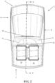
- FIG. 2 is a top view of device housing 1, which illustrates the components mentioned above in another perspective, such that left side 9 is partially visible.
- the upper light device 10 spans a substantially linear distance along the front 2 of the device housing 1.
- the lower light device 12 spans a substantially linear distance, which is vertically offset from upper light device 10, along the front 2 of the device housing 1.
- the upper light device 10 can be included at or near the transition between the front 2 and the top 6.
- the lower light device 12 can be included at or near the transition between the front 2 and the front light face 4.
- the upper light device 10 can be separate from, and not contact the device housing 1.
- the lower light device 12 can be separate from, and not contact the device housing 1.
- FIG. 3 A cross section of the device housing 1, along line 3' (shown in FIG. 2 ) is shown in FIG. 3 .
- the interior of device housing 1 is shown as hollow in this figure, to aid in explanation, with an interior surface of left side 9 visible.
- the interior of device housing 1 can include any suitable electrical apparatus and any suitable analytical apparatus.
- FIG. 3 illustrates some more details regarding upper light device 10 and lower light device 12, further detail is provided in the subsequent images, which offer magnified views of these components.
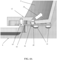
- FIG. 4A A magnified view of a cross section (from FIG. 3 ) of the lower light device 12 is shown in FIG. 4A .
- the lower light device 12 is connected to the device housing by one or more mounting elements 14.
- the mounting elements 14 are shown as screws, but in other embodiments, the mounting elements 14 can be any suitable mechanism that is capable of maintaining the lower light device 12's position within the device housing, such as a clip, snap, nail, staple and/or adhesive.
- the lower light device 12 includes a printed circuit board (electrical supply) 16, which supports one or more light emitting diodes (LEDs) 18.
- the printed circuit board 16 can be any suitable structure that can physically support the one or more LEDs 18, and also provide electricity to each of the one or more LEDs 18.
- the printed circuit board 16 can be formed of any suitable material.
- a divergence angle of the LEDs 18, as well as other LEDs disclosed in the present application is about 120°, but, can be any angle between about 90° and about 180°. Further, LEDs 18, as well as other LEDs disclosed in the present application, are capable of producing various colors (including but not limited to white, blue, green, red, and yellow), various brightnesses of light and various warmth values of light.
- LEDs 18 can extend along any portion, or the entire, length of the lower light device 12.
- the spacing between adjacent LEDs 18 can be any suitable size for the desired application.
- a light pipe 20 is located between the one or more LEDs 18 and the front light face 4.
- the spacing between adjacent LEDs 18 can be such that overlapping regions of illumination are formed by the one or more LEDs 18 in the direction of arrow 22, toward the front light face 4.
- each of the LEDs 18 can be included in upper light device 10, each of which can be spaced apart about 0.16" from center to center (about 0.05" separation between each individual LED). In other embodiments of forming overlapping regions of illumination, each of the LEDs 18 can be spaced apart from about 0.02" to about 0.10" from each other. As one of ordinary skill can determine, for housings smaller or larger than device housing 1, a fewer or more LEDs than thirty may be used.
- light pipe refers to any optical device or combination of devices having a collecting surface (for example, 42 of light pipe 20, 58 of light pipe 30 (discussed below)) through which light may be received into the light pipe device itself, a guide (for example, light pipe 20, light pipe 30) through which received light is directed from the collecting surface to an outlet (for example, 44 of light pipe 20, 54 and/or 56 of light pipe 30), and the outlet through which all or most of the received light is emitted.
- a collecting surface for example, 42 of light pipe 20, 58 of light pipe 30 (discussed below)
- a guide for example, light pipe 20, light pipe 30
- an outlet for example, 44 of light pipe 20, 54 and/or 56 of light pipe 30
- Those of skill in the art can substitute or use any suitable device or structure that is capable of receiving light through any collecting surface, and capable of guiding the received light through the device or structure to an outlet.
- the light pipe generally comprises an elongated transparent or translucent member having a collecting surface, a guide portion with reflection surfaces and an emission outlet.
- the light pipe When a light ray is directed at the collecting surface portion of the light pipe, the light is received in the guide and reflected along a trajectory toward an outlet adjacent to or abutting an optical sensor.
- the light pipe facilitates total internal reflection of the light and hence passes most or all of the light to the emission outlet.
- the light pipe 20 can be formed of one or more suitable materials, such as plastics, glasses, and combinations thereof.
- light is accepted into light pipe 20 through a face of the light pipe 20 that contacts the one or more LEDs 18.
- Light is emitted from light pipe 20 in the direction of arrow 22, towards the front light face 4.
- the light emitted from the light pipe 20 towards the front light face can be relatively uniform, due to the spacing between adjacent LEDs 18, and the structure of the light pipe 20, so that overlapping regions of illumination are formed toward the front light face 4. This relatively uniform light can be achieved without the inclusion of one or more Fresnel lenses.
- the light pipe 20 can be of a shape shown in FIG. 4A , which directs light generated by the one or more LEDs 18 more generally towards the entire surface of the front light face 4.
- a vertically thicker light pipe 20 in this structure would typically direct more light from the one or more LEDs 18 towards the vertical bottom portion of the front light face 4, with the individual locations of each of the one or more LEDs 18 more noticeable due to this direction of light.
- the height (thickness) of the light pipe 20 can be any suitable thickness, such as, for example between about 0.05" (0.127 cm) to about 0.15" (0.381 cm), about 0.07" (0.178 cm) to about 0.143" (0.363 cm), about 0.08" (0.2032 cm) to about 0.125" (0.318 cm), about 0.085" (0.216 cm) to about 0.115" (0.292 cm), or about 0.1" (0.254 cm).
- the light pipe 20 can be formed of any suitable material, such as a polycarbonate material that can be at least partially clear, and may have either a smooth, or a textured finish on any of the surfaces of light pipe 20.
- FIG. 4B is a front view of the light pipe 20, with FIG. 4C being a cross sectional view of light pipe 20 along line A-A of FIG. 4B .
- a height 40 of the light pipe 20 is about 0.08" (0.2032 cm), but as mentioned above, in other embodiments, this distance can be smaller or larger.
- This height 40 extends between a lower surface 42 to a first upper surface 44.
- Angle B between the lower surface 42 to the first upper surface 44 is about 110°, however, in other embodiments, this angle can be 10%, 20% or more larger or smaller than about 110°.
- Angle C between a second upper surface 46 and the first upper surface 44 is about 130°, however, in other embodiments, this angle can be 10%, 20% or more larger or smaller than about 130°.
- the ratio of the height of the second upper surface 46 to the height 40 is about 50%, however, in other embodiments, this ratio can be 10%, 20% or more larger or smaller than about 50%.
- the height of the second upper surface 46 can be larger than the height 40, so that second upper surface 46 is further from the lower surface 42 than the first upper surface 44.
- an angle between the second upper surface 46 and the first upper surface 44 would be about 50° however, in other embodiments, this angle can be 10%, 20% or more larger or smaller than about 50°.
- the sum of Angles B and C is about 180° between the lower surface 42 and the second upper surface 46, however, in other embodiments, this angle can be 10%, 20% or more larger or smaller than about 180°, and, in yet other embodiments, these angles be a portion of a circumference of a circle.
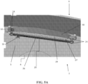
- FIG. 5A A magnified view of a perspective view of the upper light device 10 (from FIG. 3 ) is shown in FIG. 5A
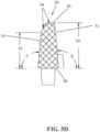
- FIG. 5B A cross section (from FIG. 3 ) of the upper light device 10 is shown in FIG. 5B .
- FIG. 5A is a perspective view of the upper light device 10, the perspective being from the rear of the device housing 1 towards the interface between the top 6 and the front light face border 5.
- the upper light device 10 is connected to the device housing by one or more mounting elements 24.
- the mounting elements 24 are shown as screws, but in other embodiments, the mounting elements 24 can be any suitable mechanism that is capable of maintaining the upper light device 10's position within the device housing, such as a clip, snap, nail, staple and/or adhesive
- the upper light device 10 includes a printed circuit board (electrical supply) 26, which supports one or more light emitting diodes (LEDs) 28.
- the printed circuit board 26 can be any suitable structure that can physically support the one or more LEDs 28, and also provide electricity to each of the one or more LEDs 28.
- the printed circuit board 26 can be formed of any suitable material.
- LEDs 28 can extend along any portion, or the entire, length of the upper light device 10.
- the spacing between adjacent LEDs 28 can be any suitable size for the desired application.
- the spacing between adjacent LEDs 28 can be such that overlapping regions of illumination are formed by the one or more LEDs 28.
- about twenty four LEDs 28 can be included in lower light device 12, each of which can be spaced apart about 0.30" (0.762 cm) from center to center (about 0.19" (0.483 cm) between each individual LED).
- each of the LEDs 28 can be spaced apart from about 0.1" (0.254 cm) to about 0.40" (1.016 cm) from each other. As one of ordinary skill can determine, for housings smaller or larger than device housing 1, fewer or more LEDs than twenty four may be used.
- This space 27 can be any suitable size, or not present at all.
- the space 27 can be between about 0.05" (0.127 cm) to about 0.15" (0.381 cm), about 0.07"(0.178 cm) to about 0.143" (0.363 cm), about 0.08" (0.2032 cm)to about 0.125" (0.318 cm), about 0.085" (0.216 cm) to about 0.115" (0.216 cm), or about 0.090" (0.229 cm).
- the space 27 can be configured to be a distance that is large enough to allow the light from the LEDs 28 to partially scatter/spread before reaching the light pipe 30, but a distance that is small enough that the majority of the light from the LEDs 28 pass through the light pipe 30.
- the diffuser film 29 receives the light from the one or more LEDs 28, transmits the light, and contacts a light pipe 30.
- the term, "diffuser film” means any material, of any suitable thickness, that is able to scatter specular light (light with a primary direction) at many angles to produce a diffuse light (light with random light direction).
- the diffuser film 29 can be made of any suitable material, such as from one or more polymers, glass or paper.
- the diffuser film 29 can be transparent or translucent.
- the diffuser film 29 can be an engineered diffuser with patterns embossed onto the surface of the film.
- the diffuser film 29 can be a holographic diffuser fabricated by recording laser speckle patterns onto a photoresist or film.
- the diffuser film 29 can be a diffractive diffuser or a material with particulate additives for scattering light.
- a diffuser film 29 Some non-limiting examples of a diffuser film 29 are: 3M TM Envision TM Diffuser Film 3735-50; DFPM grade circular diffuser film supplied by Grafix plastics; and EDF-L1 Engineered diffuser film supplied by RPC Photonics, Inc.
- An electrical connector 32 is also illustrated in FIG. 5A , which can be configured to connect to any suitable incoming electrical signal, which will be delivered to the one or more LEDs 28.
- the light pipe 30 forms a portion of the exterior surface of the device housing 1, forming a portion of an edge between the front light face border 5 and the top 6.
- FIG. 5C is a front view of the light pipe 30, with FIG. 5D being a cross sectional view of light pipe 30 along line A-A of FIG. 5C .
- the light pipe 30 can be formed of any suitable material, such as a polycarbonate material that can be at least partially clear, and may have either a smooth, or a textured finish on any of the surfaces of light pipe 30.
- the light emitted from the light pipe 30 can be relatively uniform, due to the spacing between adjacent LEDs 28, and the structure of the light pipe 30, so that overlapping regions of illumination are formed in a direction away from the light pipe 30. This relatively uniform light can be achieved without the inclusion of one or more Fresnel lenses.
- a first height 50 of the light pipe 30 is about 0.65"
- a second height 52 is about 0.52"
- the first height 50 and the second height 52 can be 10%, 20% or more larger or smaller than each of these dimensions.
- the first height 50 extends from a top surface 56 to a bottom surface 58 along a first height surface 51.
- the second height 52 extends from the bottom surface 58 to the bottom of portions 54 along a second height surface 53.
- the difference in height between the first height 50 and the second height 52 is variable based on the portions 54 of the light pipe 30.
- the portions 54 can be angled and/or curved, and in some embodiments, form a surface of a device housing or device.
- the second height 52 can be the same or substantially the same as the first height 50. In yet other embodiments, the second height 52 can be larger than the first height 50.
- Angle D between the lower surface 58, and the first height surface 51 is about 95°, however, in other embodiments, this angle can be 10%, 20% or more greater or less than about 95°.
- Angle E between the lower surface 58 and the second height surface 53 is about 95°, however, in other embodiments, this angle can be 10%, 20% or more greater or less than about 95°.
- upper light device 10 and lower light device 12 have been described above in reference to the device shown in FIGs. 1-3 , the location of upper light device 10 and lower light device 12 can be other locations in or on device housing 1.
- upper light device 10 and lower light device 12 can be included in and/or on various other pieces of equipment or apparatuses, described above such as a computer (e.g., a laptop computer), kitchen appliance, or consumer electronic equipment to provide utilitarian or aesthetic illumination as described above.
- a computer e.g., a laptop computer
- kitchen appliance e.g., a kitchen appliance
- consumer electronic equipment e.g., a consumer electronic equipment to provide utilitarian or aesthetic illumination as described above.
- upper light device 10 and lower light device 12 can be included in and/or on a mobile device such as a smart phone.
- Another aspect described herein is a method of manufacturing the upper light device 10, the lower light device 12, the device housing 1, and modifications and variations thereof as described.
- Another aspect described herein is a method of lighting a surface of a device housing
- the spacing of LEDs 28 of the upper light device 10 and the spacing of LEDs 18 of lower light device 12 can be configured so that the distance between each of the LEDs forms overlapping regions of illumination on a surface of the device housing 1.
- the LEDs 28 of the upper light device 10 and the LEDs 18 of lower light device 12 can be supplied with an electrical signal continuously, for a period of time, so that the LEDs 28 of the upper light device 10 and the LEDs 18 of lower light device 12 continuously illuminate at a first color.
- a continuous illumination of green or blue can indicate that a device within the device housing 1 is powered, but idle.
- the LEDs 28 of the upper light device 10 and the LEDs 18 of lower light device 12 can be supplied with an electrical signal continuously, for a period of time, so that the LEDs 28 of the upper light device 10 and the LEDs 18 of lower light device 12 continuously illuminate at a second color, different from the first color.
- a continuous illumination of red or yellow can indicate that a device within the device housing 1 is in a fault state due, for example, to the device not being ready to conduct the activity, or that attention is required from a user.
- the LEDs 28 of the upper light device 10 and the LEDs 18 of lower light device 12 can be supplied with an electrical signal in a pulsed sequence over a length of time so that the LEDs 28 of the upper light device 10 and the LEDs 18 of lower light device 12 are supplied for a period of time to illuminate the LEDs 28 of the upper light device 10 and the LEDs 18 of lower light device 12 at a first color (different or the same as the first color that is continuously illuminated) followed by not being supplied for a period of time.
- this alternate illumination can be of green or blue and can indicate that a device within the device housing 1 is operating or operational.
- the intensity of light illuminated from the LEDs 28 of the upper light device 10 and the LEDs 18 of lower light device 12 can be increased or decreased.
- the device housing 1 comprises an AC to DC converter.
- the converter is configured to convert a power source, such as a wall power supply into a DC link voltage.
- a wall power supply may be 120VAC @ 60Hz.
- the wall power supply may be 240VAC or another AC voltage.
- the voltage of the DC link may be defined as needed.
- the DC link voltage may be based on the number of LEDs used and its configuration.
- the LEDs 18 or 28 may be serially connected.
- the DC link voltage is a sum of the voltage required to operate each LED.
- the device housing 1 may comprise an internal power supply such as a battery.
- the battery will provide DC voltage.
- the device housing 1 may also include a DC to DC converter. Where multiple LEDs 18 or 28 are connected in series, the DC to DC converter may be a boost converter, which increases the voltage from the battery voltage provided.
- the device housing 1 may further comprise a pulse width modulation (PWM) circuit that controls the duty cycle of the supplied voltage to the LEDs 18 or 28.
- PWM pulse width modulation
- the PWM circuit controls the intensity of the light emitted by the LEDs.
- the PWM circuit may be implemented as a 555 timer PWM.
- the PWM circuit may be connected with a dimmer switch to change the intensity of the LEDs.
- the dimmer switch may be a potentiometer (POT).
- POT potentiometer
- the POT may be disposed anywhere in or on the device housing 1, or, the POT can be disposed outside the device housing 1.
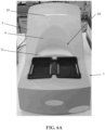
- FIG. 6A One embodiment of device housing 1 is shown in FIG. 6A .
- the device housing 1 includes the front 2, the front light face 4, and the front light face border 5.
- the upper light device 10 spans a substantially linear distance along the front 2 of the device housing 1.
- the lower light device 12 spans a substantially linear distance along the front 2 of the device housing 1 .
- the lower light device 12 is illuminated, and is forming an area of illumination 60 on the front light face 4.
- This area of illumination 60 is formed due to the illumination of LEDs 18(shown in FIG. 4A ) illuminating overlapping regions of illumination on the surface of the front light face 4.
- the area of illumination 60 is relatively uniform from a left side of the front light face 4 to a right side of the front light face 4.
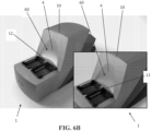
- FIG. 6B Another embodiment of device housing 1 is shown in FIG. 6B , with two different statuses identified.
- the area of illumination 60 on the front light face, as a result of illumination by the lower light device 12, and the upper light device 10, are both illuminated in a first steady-state color of blue.
- this color blue indicates that the instrument in the device housing 1 is turned on, but idle.
- the area of illumination 60 on the front light face, as a result of illumination by the lower light device 12, and the upper light device 10, are both illuminated in a first steady-state color of red.
- this color red indicates that the instrument in the device housing 1 is in a fault state due, for example, to the device not being ready to conduct the activity, or that attention is required from a user.
- the same PWM circuit may be used to control both sets of LEDs 18/28.
- two separate PWM circuits are independently used to control the respective sets of LEDs 18 or 28.
- One PWM circuit is installed in the printed circuit board 16 and another PWM circuit is installed in the printed circuit board 26.
- separate and independent DC to DC converters or AC to DC converters would be installed in the respective printed circuit boards.
- a current limiting resistor R is placed in series with the LEDs.
- the current limiting resistor R has a resistance configured to keep the current at a specified level. Where the LEDs 18 are in parallel, a current limiting resistor R will be placed in series with each LED 18.
- the upper light device 10 and lower light device 12 are described herein as being included in a specific device housing, however, in other embodiments one or both of the upper light device 10 and lower light device 12 can be included in any other suitable housing, device, or surface.
Landscapes
- Physics & Mathematics (AREA)
- General Physics & Mathematics (AREA)
- Engineering & Computer Science (AREA)
- General Engineering & Computer Science (AREA)
- Optics & Photonics (AREA)
- Analytical Chemistry (AREA)
- Life Sciences & Earth Sciences (AREA)
- Chemical & Material Sciences (AREA)
- Health & Medical Sciences (AREA)
- Biochemistry (AREA)
- General Health & Medical Sciences (AREA)
- Immunology (AREA)
- Pathology (AREA)
- Electromagnetism (AREA)
- Non-Portable Lighting Devices Or Systems Thereof (AREA)
- Arrangement Of Elements, Cooling, Sealing, Or The Like Of Lighting Devices (AREA)
- Planar Illumination Modules (AREA)
- Illuminated Signs And Luminous Advertising (AREA)
Description
- This application claims the benefit of
U.S. Provisional Application No. 62/956,983 filed on January 3, 2020 - Methods and devices have been developed for lighting support structures such as housings for apparatuses including those for conducting chemical, biochemical, and/or biological assays, housings for consumer products such as computers, kitchen appliances, and electronics, structures for automotive interiors and exteriors, and structures for architectural details. These methods and devices are used in a variety of applications including medical diagnostics, food and beverage testing, environmental monitoring, manufacturing quality control, drug discovery, basic scientific research, automotive, cooking, and interior design. These uses may be for utilitarian and aesthetic purposes. For example, utilitarian reasons include showing the status of an apparatus contained in the housing (e.g., via color or intermittent flashing or pulsing), or lighting a display on the housing for visualization by a user.
- A variety of apparatuses are available for conducting assay measurements including instruments that measure changes in optical absorbance, emission of luminescence (e.g., fluorescence, phosphorescence, chemiluminescence, and electrochemiluminescence (ECL)), emission of radiation, changes in light scattering, and changes in a magnetic field.
U.S. Patent Application Publications 2004/0022677 and2005/0052646 describe solutions that are useful for carrying out singleplex and multiplex ECL assays in a multi-well plate format. They include plates that comprise a plate top with through-holes that form the walls of the wells and a plate bottom that is sealed against the plate top to form the bottom of the wells. The plate bottom has patterned conductive layers that provide the wells with electrode surfaces that act as both solid phase supports for binding reactions as well as electrodes for inducing ECL. The conductive layers may also include electrical contacts for applying electrical energy to the electrode surfaces. Reference is also made toU.S. application Ser. No. 11/642,968 . - Challenges arise for developing methods and devices for lighting support structures, e.g., housings, when the surface of the support structure contains a shape such as an angle, curve (convex or concave), or indentation.
US5572613 ,US2014/340927 ,US4106231 andUS2013/300979 each disclose a housing comprising a light device. - Thus, improved methods and devices for lighting are needed for aesthetic and utilitarian reasons. Some improvements resulting from the disclosed methods and devices result in a more even distribution of light across a surface of a housing due to the structure of the light devices disclosed below. The disclosed light devices are engineered to have a compact, low-profile design, be easily manufactured, and not require Fresnel lenses.
- The present invention is directed to a device housing comprising the features of
claim 1. Preferred embodiments of the invention are subject of the depending claims. - The file of this patent contains at least one drawing executed in color. Copies of this patent with color drawing(s) will be provided by the Patent and Trademark Office upon request and payment of the necessary fee.
- The present disclosure will be better understood by reference to the following drawings, which are provided as illustrative of certain embodiments of the subject application, and not meant to limit the scope of the present disclosure.
-
FIG. 1 is a graphical illustration of a perspective view of a device housing. -
FIG. 2 is a graphical illustration of a top view of the device housing -
FIG. 3 is a graphical illustration of a cross-sectional view of the device housing. -
FIG. 4A-4C are views of the lower light device. -
FIGs. 5A-5D are views of the upper light device. -
FIG. 6A is a photograph of one example of a device housing. -
FIG. 6B is a rendering of two examples of device housings. - In the discussion and claims herein, the term "about" indicates that the value listed may be somewhat altered, as long as the alteration does not result in nonconformance of the process or device. For example, for some elements the term "about" can refer to a variation of ±0.1%, for other elements, the term "about" can refer to a variation of ±1% or ±10%, or any point therein.
- As used herein, the term "substantially", or "substantial", is equally applicable when used in a negative connotation to refer to the complete or near complete lack of an action, characteristic, property, state, structure, item, or result. For example, a surface that is "substantially" flat would either completely flat, or so nearly flat that the effect would be the same as if it were completely flat.
- As used herein terms such as "a", "an" and "the" are not intended to refer to only a singular entity, but include the general class of which a specific example may be used for illustration.
- As used herein, terms defined in the singular are intended to include those terms defined in the plural and vice versa.
- References in the specification to "one embodiment", "certain embodiments", some embodiments" or "an embodiment", indicate that the embodiment(s) described may include a particular feature or characteristic, but every embodiment may not necessarily include the particular feature, structure, or characteristic. Moreover, such phrases are not necessarily referring to the same embodiment. Further, when a particular feature, structure, or characteristic is described in connection with an embodiment, it is submitted that it is within the knowledge of one skilled in the art to affect such feature, structure, or characteristic in connection with other embodiments whether or not explicitly described. For purposes of the description hereinafter, the terms "upper", "lower", "right", "left", "vertical", "horizontal", "top", "bottom", and derivatives thereof shall relate to the invention, as it is oriented in the drawing figures. The terms "overlying", "atop", "positioned on" or "positioned atop" means that a first element, is present on a second element, wherein intervening elements interface between the first element and the second element. The term "direct contact" or "attached to" means that a first element, and a second element are connected without any intermediary element at the interface of the two elements.
- Reference herein to any numerical range expressly includes each numerical value (including fractional numbers and whole numbers) encompassed by that range. To illustrate, reference herein to a range of "at least 50" or "at least about 50" includes whole numbers of 50, 51, 52, 53, 54, 55, 56, 57, 58, 59, 60, etc., and fractional numbers 50.1, 50.2 50.3, 50.4, 50.5, 50.6, 50.7, 50.8, 50.9, etc. In a further illustration, reference herein to a range of "less than 50" or "less than about 50" includes
whole numbers -
FIG. 1 is an illustration of adevice housing 1. Thedevice housing 1 is an example of a structure that is capable of containing one, two, or more light devices described in the present disclosure. In other embodiments, the one or more light devices described in the present disclosure can be included in any other suitable housing and/or support structure. - The
device housing 1 includes afront 2, afront light face 4, a frontlight face border 5, atop 6, and aright side 8. Also included are a left side and bottom of the device housing, although these features are not illustrated. Also included in thedevice housing 1 is an upper light device 10 (also referred to as first light device) and a lower light device 12 (also referred to as second light device), each of which will be discussed in more detail below. In other embodiments, the size and location of these light devices can be different. Either or both of theupper light device 10 and thelower light device 12 can display various colors and/or intensities of light, which can act as status identifiers. For example, a first steady-state color (e.g., blue or green) indicates that the instrument in the housing is turned on but idle, a second steady-state color (e.g., red or yellow) indicates that the instrument in the housing is either not ready or requires attention (e.g., a fault state), and a pulsing color (e.g., blue or green) indicates that the instrument is turned on and operating or operational. - In this example of
device housing 1,front light face 4 is shown as a substantially curved, flat structure, but in other embodiments,front light face 4 can be formed of different flat shapes, or, can be other angular and/or curved shapes. - Although not shown,
device housing 1 can include various electrical and internet connections, either, wired or wireless, to provide electricity and information/communication ability to thedevice housing 1. - As seen in
FIG. 1 , thedevice housing 1 can include several surfaces, each of which can be formed of the same, or different material. The material is any suitable material selected from metals, plastic based materials, rubbers, carbon based materials, glasses, and combinations thereof. - Each surface of the
device housing 1 can include a layer of paint, and/or an adhesive element (such as a sticker and/or an adhesive wrap), and/or no extra material on the outer surface of the material that forms that portion of thedevice housing 1. - Each surface of the
device housing 1 can be finished in any suitable way, such as with a matte finish, a shiny finish, and levels of light reflectance in between. -
FIG. 2 is a top view ofdevice housing 1, which illustrates the components mentioned above in another perspective, such thatleft side 9 is partially visible. As can be seen inFIG. 2 , the upperlight device 10 spans a substantially linear distance along thefront 2 of thedevice housing 1. Also, the lowerlight device 12 spans a substantially linear distance, which is vertically offset from upperlight device 10, along thefront 2 of thedevice housing 1. The upperlight device 10 can be included at or near the transition between the front 2 and the top 6. The lowerlight device 12 can be included at or near the transition between the front 2 and thefront light face 4. In other embodiments, the upperlight device 10 can be separate from, and not contact thedevice housing 1. In other embodiments, the lowerlight device 12 can be separate from, and not contact thedevice housing 1. - A cross section of the
device housing 1, along line 3' (shown inFIG. 2 ) is shown inFIG. 3 . The interior ofdevice housing 1 is shown as hollow in this figure, to aid in explanation, with an interior surface ofleft side 9 visible. However, the interior ofdevice housing 1 can include any suitable electrical apparatus and any suitable analytical apparatus. - Although
FIG. 3 illustrates some more details regarding upperlight device 10 and lowerlight device 12, further detail is provided in the subsequent images, which offer magnified views of these components. - A magnified view of a cross section (from
FIG. 3 ) of the lowerlight device 12 is shown inFIG. 4A . The lowerlight device 12 is connected to the device housing by one or moremounting elements 14. In this embodiment the mountingelements 14 are shown as screws, but in other embodiments, the mountingelements 14 can be any suitable mechanism that is capable of maintaining the lowerlight device 12's position within the device housing, such as a clip, snap, nail, staple and/or adhesive. - The lower
light device 12 includes a printed circuit board (electrical supply) 16, which supports one or more light emitting diodes (LEDs) 18. The printedcircuit board 16 can be any suitable structure that can physically support the one ormore LEDs 18, and also provide electricity to each of the one ormore LEDs 18. The printedcircuit board 16 can be formed of any suitable material. - A divergence angle of the
LEDs 18, as well as other LEDs disclosed in the present application, is about 120°, but, can be any angle between about 90° and about 180°. Further,LEDs 18, as well as other LEDs disclosed in the present application, are capable of producing various colors (including but not limited to white, blue, green, red, and yellow), various brightnesses of light and various warmth values of light. - Only one
full LED 18 is shown inFIG. 4A , however,LEDs 18 can extend along any portion, or the entire, length of the lowerlight device 12. The spacing betweenadjacent LEDs 18 can be any suitable size for the desired application. - To guide light generated from the one or
more LEDs 18, alight pipe 20 is located between the one ormore LEDs 18 and thefront light face 4. For example, the spacing betweenadjacent LEDs 18 can be such that overlapping regions of illumination are formed by the one ormore LEDs 18 in the direction ofarrow 22, toward thefront light face 4. - As one non-limiting example of forming overlapping regions of illumination, about thirty
LEDs 18 can be included in upperlight device 10, each of which can be spaced apart about 0.16" from center to center (about 0.05" separation between each individual LED). In other embodiments of forming overlapping regions of illumination, each of theLEDs 18 can be spaced apart from about 0.02" to about 0.10" from each other. As one of ordinary skill can determine, for housings smaller or larger thandevice housing 1, a fewer or more LEDs than thirty may be used. - The term "light pipe" refers to any optical device or combination of devices having a collecting surface (for example, 42 of
light pipe light pipe 20, light pipe 30) through which received light is directed from the collecting surface to an outlet (for example, 44 oflight pipe - In one embodiment, the light pipe generally comprises an elongated transparent or translucent member having a collecting surface, a guide portion with reflection surfaces and an emission outlet. When a light ray is directed at the collecting surface portion of the light pipe, the light is received in the guide and reflected along a trajectory toward an outlet adjacent to or abutting an optical sensor. The light pipe facilitates total internal reflection of the light and hence passes most or all of the light to the emission outlet.
- In this disclosure, the
light pipe 20 can be formed of one or more suitable materials, such as plastics, glasses, and combinations thereof. - In
FIG. 4A , light is accepted intolight pipe 20 through a face of thelight pipe 20 that contacts the one ormore LEDs 18. Light is emitted fromlight pipe 20 in the direction ofarrow 22, towards thefront light face 4. The light emitted from thelight pipe 20 towards the front light face can be relatively uniform, due to the spacing betweenadjacent LEDs 18, and the structure of thelight pipe 20, so that overlapping regions of illumination are formed toward thefront light face 4. This relatively uniform light can be achieved without the inclusion of one or more Fresnel lenses. - The
light pipe 20 can be of a shape shown inFIG. 4A , which directs light generated by the one ormore LEDs 18 more generally towards the entire surface of thefront light face 4. A vertically thickerlight pipe 20 in this structure would typically direct more light from the one ormore LEDs 18 towards the vertical bottom portion of thefront light face 4, with the individual locations of each of the one ormore LEDs 18 more noticeable due to this direction of light. - The height (thickness) of the
light pipe 20 can be any suitable thickness, such as, for example between about 0.05" (0.127 cm) to about 0.15" (0.381 cm), about 0.07" (0.178 cm) to about 0.143" (0.363 cm), about 0.08" (0.2032 cm) to about 0.125" (0.318 cm), about 0.085" (0.216 cm) to about 0.115" (0.292 cm), or about 0.1" (0.254 cm). Also, thelight pipe 20 can be formed of any suitable material, such as a polycarbonate material that can be at least partially clear, and may have either a smooth, or a textured finish on any of the surfaces oflight pipe 20. - A more detailed view of the
light pipe 20 is shown inFIG. 4B. FIG. 4B is a front view of thelight pipe 20, withFIG. 4C being a cross sectional view oflight pipe 20 along line A-A ofFIG. 4B . - In
FIG. 4C , aheight 40 of thelight pipe 20 is about 0.08" (0.2032 cm), but as mentioned above, in other embodiments, this distance can be smaller or larger. Thisheight 40 extends between alower surface 42 to a firstupper surface 44. Angle B between thelower surface 42 to the firstupper surface 44 is about 110°, however, in other embodiments, this angle can be 10%, 20% or more larger or smaller than about 110°. Angle C between a secondupper surface 46 and the firstupper surface 44 is about 130°, however, in other embodiments, this angle can be 10%, 20% or more larger or smaller than about 130°. - In the embodiment shown in
FIG. 4C , the ratio of the height of the secondupper surface 46 to theheight 40 is about 50%, however, in other embodiments, this ratio can be 10%, 20% or more larger or smaller than about 50%. - In other embodiments, the height of the second
upper surface 46 can be larger than theheight 40, so that secondupper surface 46 is further from thelower surface 42 than the firstupper surface 44. In this embodiment an angle between the secondupper surface 46 and the firstupper surface 44 would be about 50° however, in other embodiments, this angle can be 10%, 20% or more larger or smaller than about 50°. - Also as can be seen in
FIG. 4C , the sum of Angles B and C is about 180° between thelower surface 42 and the secondupper surface 46, however, in other embodiments, this angle can be 10%, 20% or more larger or smaller than about 180°, and, in yet other embodiments, these angles be a portion of a circumference of a circle. - A magnified view of a perspective view of the upper light device 10 (from
FIG. 3 ) is shown inFIG. 5A , a cross section (fromFIG. 3 ) of the upperlight device 10 is shown inFIG. 5B . -
FIG. 5A is a perspective view of the upperlight device 10, the perspective being from the rear of thedevice housing 1 towards the interface between the top 6 and the frontlight face border 5. The upperlight device 10 is connected to the device housing by one or moremounting elements 24. In this embodiment the mountingelements 24 are shown as screws, but in other embodiments, the mountingelements 24 can be any suitable mechanism that is capable of maintaining the upperlight device 10's position within the device housing, such as a clip, snap, nail, staple and/or adhesive - The upper
light device 10 includes a printed circuit board (electrical supply) 26, which supports one or more light emitting diodes (LEDs) 28. The printedcircuit board 26 can be any suitable structure that can physically support the one ormore LEDs 28, and also provide electricity to each of the one ormore LEDs 28. The printedcircuit board 26 can be formed of any suitable material. -
Several LEDs 28 are shown inFIG. 5A , however,LEDs 28 can extend along any portion, or the entire, length of the upperlight device 10. The spacing betweenadjacent LEDs 28 can be any suitable size for the desired application. For example, the spacing betweenadjacent LEDs 28 can be such that overlapping regions of illumination are formed by the one ormore LEDs 28. As one non-limiting example of forming overlapping regions of illumination, about twenty fourLEDs 28 can be included in lowerlight device 12, each of which can be spaced apart about 0.30" (0.762 cm) from center to center (about 0.19" (0.483 cm) between each individual LED). In other embodiments of forming overlapping regions of illumination, each of theLEDs 28 can be spaced apart from about 0.1" (0.254 cm) to about 0.40" (1.016 cm) from each other. As one of ordinary skill can determine, for housings smaller or larger thandevice housing 1, fewer or more LEDs than twenty four may be used. - Vertically between the one or
more LEDs 28 and adiffuser film 29 is aspace 27. Thisspace 27 can be any suitable size, or not present at all. Thespace 27 can be between about 0.05" (0.127 cm) to about 0.15" (0.381 cm), about 0.07"(0.178 cm) to about 0.143" (0.363 cm), about 0.08" (0.2032 cm)to about 0.125" (0.318 cm), about 0.085" (0.216 cm) to about 0.115" (0.216 cm), or about 0.090" (0.229 cm). In other embodiments, thespace 27 can be configured to be a distance that is large enough to allow the light from theLEDs 28 to partially scatter/spread before reaching thelight pipe 30, but a distance that is small enough that the majority of the light from theLEDs 28 pass through thelight pipe 30. - The
diffuser film 29 receives the light from the one ormore LEDs 28, transmits the light, and contacts alight pipe 30. As used herein the term, "diffuser film" means any material, of any suitable thickness, that is able to scatter specular light (light with a primary direction) at many angles to produce a diffuse light (light with random light direction). Thediffuser film 29 can be made of any suitable material, such as from one or more polymers, glass or paper. Thediffuser film 29 can be transparent or translucent. In other embodiments, thediffuser film 29 can be an engineered diffuser with patterns embossed onto the surface of the film. In other embodiments, thediffuser film 29 can be a holographic diffuser fabricated by recording laser speckle patterns onto a photoresist or film. In other embodiments, thediffuser film 29 can be a diffractive diffuser or a material with particulate additives for scattering light. - Some non-limiting examples of a
diffuser film 29 are: 3M™ Envision™ Diffuser Film 3735-50; DFPM grade circular diffuser film supplied by Grafix plastics; and EDF-L1 Engineered diffuser film supplied by RPC Photonics, Inc. - An
electrical connector 32 is also illustrated inFIG. 5A , which can be configured to connect to any suitable incoming electrical signal, which will be delivered to the one ormore LEDs 28. - As can be seen in
FIG. 5B , thelight pipe 30 forms a portion of the exterior surface of thedevice housing 1, forming a portion of an edge between the frontlight face border 5 and the top 6. - A more detailed view of the
light pipe 30 is shown inFIG. 5C. FIG. 5C is a front view of thelight pipe 30, withFIG. 5D being a cross sectional view oflight pipe 30 along line A-A ofFIG. 5C . Thelight pipe 30 can be formed of any suitable material, such as a polycarbonate material that can be at least partially clear, and may have either a smooth, or a textured finish on any of the surfaces oflight pipe 30. The light emitted from thelight pipe 30 can be relatively uniform, due to the spacing betweenadjacent LEDs 28, and the structure of thelight pipe 30, so that overlapping regions of illumination are formed in a direction away from thelight pipe 30. This relatively uniform light can be achieved without the inclusion of one or more Fresnel lenses. - In
FIG. 5D , afirst height 50 of thelight pipe 30 is about 0.65", asecond height 52 is about 0.52", however, thefirst height 50 and thesecond height 52 can be 10%, 20% or more larger or smaller than each of these dimensions. Thefirst height 50 extends from atop surface 56 to abottom surface 58 along afirst height surface 51. Thesecond height 52 extends from thebottom surface 58 to the bottom ofportions 54 along asecond height surface 53. - The difference in height between the
first height 50 and thesecond height 52 is variable based on theportions 54 of thelight pipe 30. Theportions 54 can be angled and/or curved, and in some embodiments, form a surface of a device housing or device. In other embodiments, thesecond height 52 can be the same or substantially the same as thefirst height 50. In yet other embodiments, thesecond height 52 can be larger than thefirst height 50. - Angle D between the
lower surface 58, and thefirst height surface 51 is about 95°, however, in other embodiments, this angle can be 10%, 20% or more greater or less than about 95°. Angle E between thelower surface 58 and thesecond height surface 53 is about 95°, however, in other embodiments, this angle can be 10%, 20% or more greater or less than about 95°. - The location of upper
light device 10 and lowerlight device 12 have been described above in reference to the device shown inFIGs. 1-3 , the location of upperlight device 10 and lowerlight device 12 can be other locations in or ondevice housing 1. - Also, although
device housing 1 has been described above in reference to the housing shown inFIGs. 1-3 , in other embodiments, one or both of upperlight device 10 and lowerlight device 12 can be included in and/or on various other pieces of equipment or apparatuses, described above such as a computer (e.g., a laptop computer), kitchen appliance, or consumer electronic equipment to provide utilitarian or aesthetic illumination as described above. - In other embodiments, one or both of upper
light device 10 and lowerlight device 12 can be included in and/or on a mobile device such as a smart phone. - Another aspect described herein is a method of manufacturing the upper
light device 10, the lowerlight device 12, thedevice housing 1, and modifications and variations thereof as described. - Another aspect described herein is a method of lighting a surface of a device housing
- 1. In this aspect the upper
light device 10 and/or the lowerlight device 12 can be arranged in any suitable location and orientation with respect to a surface of thedevice housing 1, for example afront light face 4. The upperlight device 10 and/or the lowerlight device 12 can be supplied with an electrical signal such that theLEDs 28 of the upperlight device 10 and/or theLEDs 18 of lowerlight device 12 are illuminated. The upperlight device 10 alone can be supplied with an electrical signal, the lowerlight device 12 alone can be supplied with an electrical signal, or both the upperlight device 10 and the lowerlight device 12 can be supplied, simultaneously or alternately, with an electrical signal. - As discussed above, the spacing of
LEDs 28 of the upperlight device 10 and the spacing ofLEDs 18 of lowerlight device 12 can be configured so that the distance between each of the LEDs forms overlapping regions of illumination on a surface of thedevice housing 1. - The
LEDs 28 of the upperlight device 10 and theLEDs 18 of lowerlight device 12 can be supplied with an electrical signal continuously, for a period of time, so that theLEDs 28 of the upperlight device 10 and theLEDs 18 of lowerlight device 12 continuously illuminate at a first color. For example, a continuous illumination of green or blue can indicate that a device within thedevice housing 1 is powered, but idle. - Further, the
LEDs 28 of the upperlight device 10 and theLEDs 18 of lowerlight device 12 can be supplied with an electrical signal continuously, for a period of time, so that theLEDs 28 of the upperlight device 10 and theLEDs 18 of lowerlight device 12 continuously illuminate at a second color, different from the first color. For example, a continuous illumination of red or yellow can indicate that a device within thedevice housing 1 is in a fault state due, for example, to the device not being ready to conduct the activity, or that attention is required from a user. - The
LEDs 28 of the upperlight device 10 and theLEDs 18 of lowerlight device 12 can be supplied with an electrical signal in a pulsed sequence over a length of time so that theLEDs 28 of the upperlight device 10 and theLEDs 18 of lowerlight device 12 are supplied for a period of time to illuminate theLEDs 28 of the upperlight device 10 and theLEDs 18 of lowerlight device 12 at a first color (different or the same as the first color that is continuously illuminated) followed by not being supplied for a period of time. This gives the effect of theLEDs 28 of the upperlight device 10 and theLEDs 18 of lowerlight device 12 appearing to blink on and off over the length of time. For example, this alternate illumination can be of green or blue and can indicate that a device within thedevice housing 1 is operating or operational. - Alternatively, instead of displaying different colors for different states, the intensity of light illuminated from the
LEDs 28 of the upperlight device 10 and theLEDs 18 of lowerlight device 12 can be increased or decreased. - In an aspect of the disclosure, the
device housing 1 comprises an AC to DC converter. The converter is configured to convert a power source, such as a wall power supply into a DC link voltage. For example, a wall power supply may be 120VAC @ 60Hz. The wall power supply may be 240VAC or another AC voltage. The voltage of the DC link may be defined as needed. For example, the DC link voltage may be based on the number of LEDs used and its configuration. For example, in an aspect of the disclosure, theLEDs - In other aspects of the disclosure, instead of using an external power supply, such as a wall power supply, the
device housing 1 may comprise an internal power supply such as a battery. The battery will provide DC voltage. In accordance with this aspect of the disclosure, thedevice housing 1 may also include a DC to DC converter. Wheremultiple LEDs - The
device housing 1 may further comprise a pulse width modulation (PWM) circuit that controls the duty cycle of the supplied voltage to theLEDs - In an aspect of the disclosure, the PWM circuit may be connected with a dimmer switch to change the intensity of the LEDs. For example, the dimmer switch may be a potentiometer (POT). The POT may be disposed anywhere in or on the
device housing 1, or, the POT can be disposed outside thedevice housing 1. - One embodiment of
device housing 1 is shown inFIG. 6A . Thedevice housing 1 includes thefront 2, thefront light face 4, and the frontlight face border 5. InFIG. 6A , the upperlight device 10 spans a substantially linear distance along thefront 2 of thedevice housing 1. Also, the lowerlight device 12 spans a substantially linear distance along thefront 2 of thedevice housing 1 . - As can be seen in
FIG. 6A , the lowerlight device 12 is illuminated, and is forming an area ofillumination 60 on thefront light face 4. This area ofillumination 60 is formed due to the illumination of LEDs 18(shown inFIG. 4A ) illuminating overlapping regions of illumination on the surface of thefront light face 4. As can be seen inFIG. 6A , and inFIG. 6B discussed below, the area ofillumination 60 is relatively uniform from a left side of thefront light face 4 to a right side of thefront light face 4. - Another embodiment of
device housing 1 is shown inFIG. 6B , with two different statuses identified. - In the
device housing 1 to the left, the area ofillumination 60 on the front light face, as a result of illumination by the lowerlight device 12, and the upperlight device 10, are both illuminated in a first steady-state color of blue. In this example, this color blue indicates that the instrument in thedevice housing 1 is turned on, but idle. - In the
device housing 1 to the right (shown as an inset), the area ofillumination 60 on the front light face, as a result of illumination by the lowerlight device 12, and the upperlight device 10, are both illuminated in a first steady-state color of red. In this example, this color red indicates that the instrument in thedevice housing 1 is in a fault state due, for example, to the device not being ready to conduct the activity, or that attention is required from a user. - In an aspect of the disclosure, the same PWM circuit may be used to control both sets of
LEDs 18/28. In other aspect of the disclosure, two separate PWM circuits are independently used to control the respective sets ofLEDs circuit board 16 and another PWM circuit is installed in the printedcircuit board 26. Similarly, separate and independent DC to DC converters (or AC to DC converters) would be installed in the respective printed circuit boards. - In an aspect of the disclosure, a current limiting resistor R is placed in series with the LEDs. The current limiting resistor R has a resistance configured to keep the current at a specified level. Where the
LEDs 18 are in parallel, a current limiting resistor R will be placed in series with eachLED 18. - The upper
light device 10 and lowerlight device 12 are described herein as being included in a specific device housing, however, in other embodiments one or both of the upperlight device 10 and lowerlight device 12 can be included in any other suitable housing, device, or surface. - The described embodiments and examples of the present disclosure are intended to be illustrative rather than restrictive, and are not intended to represent every embodiment or example of the present disclosure. Further, various modifications and variations can be made without departing from the scope of the invention as set forth in the following claims.
Claims (11)
- A device housing (1) comprising:
a first light device (10), the first light device (10) comprising a first electrical supply (26) configured to provide an electrical signal to a first light emitting diode (LED) (28), the first LED (28) separated from a first surface of a diffuser film (29) by a space (27), wherein the diffuser film (29) comprises a second surface, opposite the first surface, the second surface configured to contact a first light pipe (30), characterized in that the device housing (1) further comprises a second light device (12), the second light device (12) comprising a second electrical supply (16) configured to provide an electrical signal to a second LED (18), wherein the second LED (18) contacts a second light pipe (20). - The device housing of claim 1, wherein a surface of the first light device (10) forms a portion of a surface of the device housing (1).
- The device housing of claim 1, wherein the space (27) is about 0.05" (0.127 cm) to about 0.15" (0.381 cm).
- The device housing of claim 1, wherein a height dimension of the second light pipe (20) is between about 0.05" (0.127 cm) to about 0.15" (0.381 cm).
- The device housing of claim 4, wherein the height dimension of the second light pipe (20) is about 0.08" (0.2032 cm).
- The device housing of claim 1, wherein an angle between a lower surface (42) of the second light pipe (20) and a first upper surface (44) of the second light pipe (20) is about 110°.
- The device housing of claim 1, wherein an angle between a first upper surface (44) of the second light pipe (20) and a second upper surface (46) of the second light pipe (20) is about 130°.
- The device housing of claim 1, wherein a length of a first height surface (50) of the first light pipe (30) is longer than a length of a second height surface (52) of the first light pipe (30).
- The device housing of claim 1, wherein an angle between a lower surface (58) of the first light pipe (30) and a first height surface (51) of the first light pipe (30) is about 95°.
- The device housing of claim 1, wherein an angle between a lower surface (58) of the first light pipe (30) and a second height surface (53) of the first light pipe (30) is about 95°.
- The device housing of claim 1, wherein a portion of the second light device (12) forms a portion of a surface of the device housing (1).
Priority Applications (1)
| Application Number | Priority Date | Filing Date | Title |
|---|---|---|---|
| EP25159031.1A EP4535046A3 (en) | 2020-01-03 | 2020-12-31 | Device housing with lighting |
Applications Claiming Priority (2)
| Application Number | Priority Date | Filing Date | Title |
|---|---|---|---|
| US202062956983P | 2020-01-03 | 2020-01-03 | |
| PCT/US2020/067604 WO2021138521A1 (en) | 2020-01-03 | 2020-12-31 | Device housing with lighting |
Related Child Applications (1)
| Application Number | Title | Priority Date | Filing Date |
|---|---|---|---|
| EP25159031.1A Division EP4535046A3 (en) | 2020-01-03 | 2020-12-31 | Device housing with lighting |
Publications (2)
| Publication Number | Publication Date |
|---|---|
| EP4085222A1 EP4085222A1 (en) | 2022-11-09 |
| EP4085222B1 true EP4085222B1 (en) | 2025-02-26 |
Family
ID=74554211
Family Applications (2)
| Application Number | Title | Priority Date | Filing Date |
|---|---|---|---|
| EP25159031.1A Pending EP4535046A3 (en) | 2020-01-03 | 2020-12-31 | Device housing with lighting |
| EP20851268.1A Active EP4085222B1 (en) | 2020-01-03 | 2020-12-31 | Device housing with lighting |
Family Applications Before (1)
| Application Number | Title | Priority Date | Filing Date |
|---|---|---|---|
| EP25159031.1A Pending EP4535046A3 (en) | 2020-01-03 | 2020-12-31 | Device housing with lighting |
Country Status (12)
| Country | Link |
|---|---|
| US (4) | US11525951B2 (en) |
| EP (2) | EP4535046A3 (en) |
| JP (2) | JP2023512435A (en) |
| KR (1) | KR20220119064A (en) |
| CN (2) | CN118959930A (en) |
| AU (1) | AU2020419302B2 (en) |
| CA (2) | CA3287072A1 (en) |
| DK (1) | DK4085222T3 (en) |
| ES (1) | ES3022938T3 (en) |
| FI (1) | FI4085222T3 (en) |
| IL (3) | IL293733B2 (en) |
| WO (1) | WO2021138521A1 (en) |
Families Citing this family (1)
| Publication number | Priority date | Publication date | Assignee | Title |
|---|---|---|---|---|
| KR20220119064A (en) * | 2020-01-03 | 2022-08-26 | 메소 스케일 테크놀러지즈, 엘엘시 | lighting device housing |
Family Cites Families (23)
| Publication number | Priority date | Publication date | Assignee | Title |
|---|---|---|---|---|
| US4106231A (en) * | 1976-12-06 | 1978-08-15 | Master Specialties Company | Low level light indicator |
| US5572613A (en) * | 1995-03-08 | 1996-11-05 | Siemens Rolm Communications Inc. | Multiple lightpipe device |
| EP2420824B1 (en) | 2001-06-29 | 2018-11-28 | Meso Scale Technologies LLC | Multi-well plate having an array of wells and kit for use in the conduct of an ECL assay |
| JP3838196B2 (en) * | 2002-12-24 | 2006-10-25 | ブラザー工業株式会社 | Electronics |
| JP5826522B2 (en) | 2011-06-06 | 2015-12-02 | ミネベア株式会社 | Light emitting device |
| KR102075922B1 (en) * | 2012-05-10 | 2020-02-11 | 엘지디스플레이 주식회사 | Light Guide Panel and Liquid Display Apparatus using the same |
| CN104838204A (en) | 2012-09-20 | 2015-08-12 | 汤姆逊许可公司 | Panel Lighting System |
| GB2507575B (en) * | 2012-11-06 | 2017-04-12 | Filtrona C&Sp Ltd | An authentication device |
| JP6148464B2 (en) * | 2012-12-25 | 2017-06-14 | アルパイン株式会社 | Illumination device |
| US10036517B2 (en) | 2013-05-16 | 2018-07-31 | 3M Innovative Properties Company | Lightguide as luminaire |
| KR101480134B1 (en) | 2013-05-31 | 2015-01-07 | 김진호 | Emergency guide system using led and optical fiber |
| JP6187816B2 (en) | 2013-10-07 | 2017-08-30 | パナソニックIpマネジメント株式会社 | lighting equipment |
| US9349260B2 (en) * | 2013-11-13 | 2016-05-24 | Rockwell Automation Technologies, Inc. | Sensor device with enhanced light guide visualization and related methods |
| KR102111910B1 (en) | 2013-11-29 | 2020-05-18 | 현대모비스 주식회사 | Surface Light Source Module |
| US9408282B1 (en) * | 2014-07-21 | 2016-08-02 | Astro, Inc. | Multi-purpose lightbulb |
| JP6404363B2 (en) * | 2014-12-11 | 2018-10-10 | 堺ディスプレイプロダクト株式会社 | Lighting device and display device |
| JP2016128944A (en) * | 2015-01-09 | 2016-07-14 | ホーチキ株式会社 | Alarm |
| FR3046655B1 (en) * | 2016-01-08 | 2018-02-02 | Psa Automobiles Sa. | LIGHTING OR SIGNALING OPTICAL BLOCK FOR A MOTOR VEHICLE HAVING AN OPALIN MASK |
| JP6733952B2 (en) | 2016-05-16 | 2020-08-05 | 株式会社oneA | Decorative optical member and calling device including the decorative optical member |
| JP2018106526A (en) | 2016-12-27 | 2018-07-05 | 沖電気工業株式会社 | Media processing apparatus |
| CA3038002A1 (en) * | 2018-03-28 | 2019-09-28 | Abl Ip Holding Llc | Loudspeaker luminaire with light pipe |
| EP3873853B1 (en) * | 2018-11-02 | 2025-09-17 | Crystal IS, Inc. | Systems and methods for fluid disinfection with ultraviolet light |
| KR20220119064A (en) | 2020-01-03 | 2022-08-26 | 메소 스케일 테크놀러지즈, 엘엘시 | lighting device housing |
-
2020
- 2020-12-31 KR KR1020227023816A patent/KR20220119064A/en not_active Ceased
- 2020-12-31 CA CA3287072A patent/CA3287072A1/en active Pending
- 2020-12-31 CN CN202411254413.2A patent/CN118959930A/en active Pending
- 2020-12-31 FI FIEP20851268.1T patent/FI4085222T3/en active
- 2020-12-31 JP JP2022540884A patent/JP2023512435A/en active Pending
- 2020-12-31 ES ES20851268T patent/ES3022938T3/en active Active
- 2020-12-31 AU AU2020419302A patent/AU2020419302B2/en active Active
- 2020-12-31 IL IL293733A patent/IL293733B2/en unknown
- 2020-12-31 EP EP25159031.1A patent/EP4535046A3/en active Pending
- 2020-12-31 EP EP20851268.1A patent/EP4085222B1/en active Active
- 2020-12-31 CN CN202080091262.7A patent/CN114945776B/en active Active
- 2020-12-31 WO PCT/US2020/067604 patent/WO2021138521A1/en not_active Ceased
- 2020-12-31 IL IL310728A patent/IL310728B2/en unknown
- 2020-12-31 CA CA3166431A patent/CA3166431C/en active Active
- 2020-12-31 DK DK20851268.1T patent/DK4085222T3/en active
- 2020-12-31 IL IL320153A patent/IL320153A/en unknown
- 2020-12-31 US US17/139,000 patent/US11525951B2/en active Active
-
2022
- 2022-11-14 US US17/986,182 patent/US11808962B2/en active Active
-
2023
- 2023-09-20 US US18/370,495 patent/US12117637B2/en active Active
-
2024
- 2024-08-30 US US18/820,772 patent/US12546927B2/en active Active
-
2025
- 2025-01-16 JP JP2025006243A patent/JP2025061401A/en active Pending
Also Published As
| Publication number | Publication date |
|---|---|
| IL310728A (en) | 2024-04-01 |
| EP4535046A2 (en) | 2025-04-09 |
| FI4085222T3 (en) | 2025-03-31 |
| US12546927B2 (en) | 2026-02-10 |
| US20240427071A1 (en) | 2024-12-26 |
| IL310728B1 (en) | 2025-05-01 |
| CN114945776A (en) | 2022-08-26 |
| WO2021138521A1 (en) | 2021-07-08 |
| IL320153A (en) | 2025-06-01 |
| US20210208327A1 (en) | 2021-07-08 |
| KR20220119064A (en) | 2022-08-26 |
| JP2023512435A (en) | 2023-03-27 |
| CA3166431A1 (en) | 2021-07-08 |
| DK4085222T3 (en) | 2025-03-17 |
| CN118959930A (en) | 2024-11-15 |
| EP4085222A1 (en) | 2022-11-09 |
| AU2020419302A1 (en) | 2022-06-23 |
| US12117637B2 (en) | 2024-10-15 |
| US20230070700A1 (en) | 2023-03-09 |
| IL293733A (en) | 2022-08-01 |
| US11525951B2 (en) | 2022-12-13 |
| US20240027671A1 (en) | 2024-01-25 |
| IL310728B2 (en) | 2025-09-01 |
| CN114945776B (en) | 2024-09-20 |
| AU2020419302B2 (en) | 2026-04-09 |
| JP2025061401A (en) | 2025-04-10 |
| US11808962B2 (en) | 2023-11-07 |
| EP4535046A3 (en) | 2025-08-06 |
| CA3166431C (en) | 2026-02-10 |
| IL293733B2 (en) | 2024-07-01 |
| ES3022938T3 (en) | 2025-05-29 |
| CA3287072A1 (en) | 2025-11-29 |
| IL293733B1 (en) | 2024-03-01 |
Similar Documents
| Publication | Publication Date | Title |
|---|---|---|
| US7543951B2 (en) | Methods and apparatus for providing a luminous writing surface | |
| JP5160620B2 (en) | An efficient solid-state light source that emits light in a limited area of color space | |
| US7543956B2 (en) | Configurations and methods for embedding electronics or light emitters in manufactured materials | |
| JP5227460B2 (en) | LED lighting device | |
| US8334656B2 (en) | Replaceable lighting unit with adjustable output intensity and optional capability for reporting usage information, and method of operating same | |
| US12546927B2 (en) | Device housing with lighting | |
| US20250287933A1 (en) | Electrical insect eliminator simulated flame and transparent safety cage | |
| CN104246361B (en) | Apparatus and method for the time division multiplexing switchable optical elements of controllable lighting | |
| JP2008073174A (en) | Mirror with illumination | |
| WO2011131197A1 (en) | Led light fixture with background lighting using controlled inbetween diffused light group | |
| US20140007474A1 (en) | Thin-wall panel modular light box sign and display | |
| US20260140297A1 (en) | Device housing with lighting | |
| JP2012186070A (en) | Lighting fixture | |
| US10061071B2 (en) | Panel luminaire | |
| CN101324309A (en) | lighting device | |
| JP2011243348A (en) | Light source for illumination, lighting system, and led module | |
| KR200389603Y1 (en) | electric rice warmer having mood lamp | |
| KR20180074196A (en) | Dish with light guide plate unit |
Legal Events
| Date | Code | Title | Description |
|---|---|---|---|
| STAA | Information on the status of an ep patent application or granted ep patent |
Free format text: STATUS: UNKNOWN |
|
| STAA | Information on the status of an ep patent application or granted ep patent |
Free format text: STATUS: THE INTERNATIONAL PUBLICATION HAS BEEN MADE |
|
| PUAI | Public reference made under article 153(3) epc to a published international application that has entered the european phase |
Free format text: ORIGINAL CODE: 0009012 |
|
| STAA | Information on the status of an ep patent application or granted ep patent |
Free format text: STATUS: REQUEST FOR EXAMINATION WAS MADE |
|
| 17P | Request for examination filed |
Effective date: 20220719 |
|
| AK | Designated contracting states |
Kind code of ref document: A1 Designated state(s): AL AT BE BG CH CY CZ DE DK EE ES FI FR GB GR HR HU IE IS IT LI LT LU LV MC MK MT NL NO PL PT RO RS SE SI SK SM TR |
|
| DAV | Request for validation of the european patent (deleted) | ||
| DAX | Request for extension of the european patent (deleted) | ||
| REG | Reference to a national code |
Ref country code: DE Ref legal event code: R079 Free format text: PREVIOUS MAIN CLASS: F21V0008000000 Ipc: F21V0005020000 Ref country code: DE Ref legal event code: R079 Ref document number: 602020046931 Country of ref document: DE Free format text: PREVIOUS MAIN CLASS: F21V0008000000 Ipc: F21V0005020000 |
|
| GRAP | Despatch of communication of intention to grant a patent |
Free format text: ORIGINAL CODE: EPIDOSNIGR1 |
|
| STAA | Information on the status of an ep patent application or granted ep patent |
Free format text: STATUS: GRANT OF PATENT IS INTENDED |
|
| RIC1 | Information provided on ipc code assigned before grant |
Ipc: F21Y 115/10 20160101ALN20240905BHEP Ipc: F21Y 103/10 20160101ALN20240905BHEP Ipc: G02B 5/02 20060101ALI20240905BHEP Ipc: G02B 6/00 20060101ALI20240905BHEP Ipc: G01N 35/00 20060101ALI20240905BHEP Ipc: F21V 8/00 20060101ALI20240905BHEP Ipc: F21V 15/01 20060101ALI20240905BHEP Ipc: F21V 5/02 20060101AFI20240905BHEP |
|
| INTG | Intention to grant announced |
Effective date: 20240926 |
|
| P01 | Opt-out of the competence of the unified patent court (upc) registered |
Free format text: CASE NUMBER: APP_61393/2024 Effective date: 20241115 |
|
| GRAS | Grant fee paid |
Free format text: ORIGINAL CODE: EPIDOSNIGR3 |
|
| GRAA | (expected) grant |
Free format text: ORIGINAL CODE: 0009210 |
|
| STAA | Information on the status of an ep patent application or granted ep patent |
Free format text: STATUS: THE PATENT HAS BEEN GRANTED |
|
| AK | Designated contracting states |
Kind code of ref document: B1 Designated state(s): AL AT BE BG CH CY CZ DE DK EE ES FI FR GB GR HR HU IE IS IT LI LT LU LV MC MK MT NL NO PL PT RO RS SE SI SK SM TR |
|
| REG | Reference to a national code |
Ref country code: GB Ref legal event code: FG4D |
|
| REG | Reference to a national code |
Ref country code: CH Ref legal event code: EP |
|
| REG | Reference to a national code |
Ref country code: DK Ref legal event code: T3 Effective date: 20250311 |
|
| REG | Reference to a national code |
Ref country code: DE Ref legal event code: R096 Ref document number: 602020046931 Country of ref document: DE |
|
| REG | Reference to a national code |
Ref country code: IE Ref legal event code: FG4D |
|
| REG | Reference to a national code |
Ref country code: FI Ref legal event code: FGE |
|
| REG | Reference to a national code |
Ref country code: NL Ref legal event code: FP |
|
| REG | Reference to a national code |
Ref country code: SE Ref legal event code: TRGR |
|
| REG | Reference to a national code |
Ref country code: ES Ref legal event code: FG2A Ref document number: 3022938 Country of ref document: ES Kind code of ref document: T3 Effective date: 20250529 |
|
| PG25 | Lapsed in a contracting state [announced via postgrant information from national office to epo] |
Ref country code: RS Free format text: LAPSE BECAUSE OF FAILURE TO SUBMIT A TRANSLATION OF THE DESCRIPTION OR TO PAY THE FEE WITHIN THE PRESCRIBED TIME-LIMIT Effective date: 20250526 |
|
| PG25 | Lapsed in a contracting state [announced via postgrant information from national office to epo] |
Ref country code: PL Free format text: LAPSE BECAUSE OF FAILURE TO SUBMIT A TRANSLATION OF THE DESCRIPTION OR TO PAY THE FEE WITHIN THE PRESCRIBED TIME-LIMIT Effective date: 20250226 |
|
| REG | Reference to a national code |
Ref country code: LT Ref legal event code: MG9D |
|
| PG25 | Lapsed in a contracting state [announced via postgrant information from national office to epo] |
Ref country code: IS Free format text: LAPSE BECAUSE OF FAILURE TO SUBMIT A TRANSLATION OF THE DESCRIPTION OR TO PAY THE FEE WITHIN THE PRESCRIBED TIME-LIMIT Effective date: 20250626 |
|
| PG25 | Lapsed in a contracting state [announced via postgrant information from national office to epo] |
Ref country code: HR Free format text: LAPSE BECAUSE OF FAILURE TO SUBMIT A TRANSLATION OF THE DESCRIPTION OR TO PAY THE FEE WITHIN THE PRESCRIBED TIME-LIMIT Effective date: 20250226 |
|
| PG25 | Lapsed in a contracting state [announced via postgrant information from national office to epo] |
Ref country code: PT Free format text: LAPSE BECAUSE OF FAILURE TO SUBMIT A TRANSLATION OF THE DESCRIPTION OR TO PAY THE FEE WITHIN THE PRESCRIBED TIME-LIMIT Effective date: 20250626 Ref country code: LV Free format text: LAPSE BECAUSE OF FAILURE TO SUBMIT A TRANSLATION OF THE DESCRIPTION OR TO PAY THE FEE WITHIN THE PRESCRIBED TIME-LIMIT Effective date: 20250226 |
|
| PG25 | Lapsed in a contracting state [announced via postgrant information from national office to epo] |
Ref country code: GR Free format text: LAPSE BECAUSE OF FAILURE TO SUBMIT A TRANSLATION OF THE DESCRIPTION OR TO PAY THE FEE WITHIN THE PRESCRIBED TIME-LIMIT Effective date: 20250527 Ref country code: BG Free format text: LAPSE BECAUSE OF FAILURE TO SUBMIT A TRANSLATION OF THE DESCRIPTION OR TO PAY THE FEE WITHIN THE PRESCRIBED TIME-LIMIT Effective date: 20250226 |
|
| PG25 | Lapsed in a contracting state [announced via postgrant information from national office to epo] |
Ref country code: SM Free format text: LAPSE BECAUSE OF FAILURE TO SUBMIT A TRANSLATION OF THE DESCRIPTION OR TO PAY THE FEE WITHIN THE PRESCRIBED TIME-LIMIT Effective date: 20250226 |
|
| PG25 | Lapsed in a contracting state [announced via postgrant information from national office to epo] |
Ref country code: EE Free format text: LAPSE BECAUSE OF FAILURE TO SUBMIT A TRANSLATION OF THE DESCRIPTION OR TO PAY THE FEE WITHIN THE PRESCRIBED TIME-LIMIT Effective date: 20250226 Ref country code: CZ Free format text: LAPSE BECAUSE OF FAILURE TO SUBMIT A TRANSLATION OF THE DESCRIPTION OR TO PAY THE FEE WITHIN THE PRESCRIBED TIME-LIMIT Effective date: 20250226 |
|
| PG25 | Lapsed in a contracting state [announced via postgrant information from national office to epo] |
Ref country code: RO Free format text: LAPSE BECAUSE OF FAILURE TO SUBMIT A TRANSLATION OF THE DESCRIPTION OR TO PAY THE FEE WITHIN THE PRESCRIBED TIME-LIMIT Effective date: 20250226 |
|
| PG25 | Lapsed in a contracting state [announced via postgrant information from national office to epo] |
Ref country code: SK Free format text: LAPSE BECAUSE OF FAILURE TO SUBMIT A TRANSLATION OF THE DESCRIPTION OR TO PAY THE FEE WITHIN THE PRESCRIBED TIME-LIMIT Effective date: 20250226 |
|
| PGFP | Annual fee paid to national office [announced via postgrant information from national office to epo] |
Ref country code: NL Payment date: 20251027 Year of fee payment: 6 |
|
| REG | Reference to a national code |
Ref country code: DE Ref legal event code: R097 Ref document number: 602020046931 Country of ref document: DE |
|
| PLBE | No opposition filed within time limit |
Free format text: ORIGINAL CODE: 0009261 |
|
| REG | Reference to a national code |
Ref country code: CH Ref legal event code: U11 Free format text: ST27 STATUS EVENT CODE: U-0-0-U10-U11 (AS PROVIDED BY THE NATIONAL OFFICE) Effective date: 20260101 |
|
| STAA | Information on the status of an ep patent application or granted ep patent |
Free format text: STATUS: NO OPPOSITION FILED WITHIN TIME LIMIT |
|
| PGFP | Annual fee paid to national office [announced via postgrant information from national office to epo] |
Ref country code: DE Payment date: 20251027 Year of fee payment: 6 |
|
| PGFP | Annual fee paid to national office [announced via postgrant information from national office to epo] |
Ref country code: GB Payment date: 20251027 Year of fee payment: 6 |
|
| PGFP | Annual fee paid to national office [announced via postgrant information from national office to epo] |
Ref country code: NO Payment date: 20251029 Year of fee payment: 6 |
|
| PGFP | Annual fee paid to national office [announced via postgrant information from national office to epo] |
Ref country code: AT Payment date: 20251027 Year of fee payment: 6 |
|
| PGFP | Annual fee paid to national office [announced via postgrant information from national office to epo] |
Ref country code: FI Payment date: 20251028 Year of fee payment: 6 Ref country code: DK Payment date: 20251027 Year of fee payment: 6 Ref country code: IT Payment date: 20251029 Year of fee payment: 6 |
|
| PGFP | Annual fee paid to national office [announced via postgrant information from national office to epo] |
Ref country code: FR Payment date: 20251027 Year of fee payment: 6 |
|
| PGFP | Annual fee paid to national office [announced via postgrant information from national office to epo] |
Ref country code: BE Payment date: 20251027 Year of fee payment: 6 |
|
| PGFP | Annual fee paid to national office [announced via postgrant information from national office to epo] |
Ref country code: SE Payment date: 20251027 Year of fee payment: 6 |
|
| PGFP | Annual fee paid to national office [announced via postgrant information from national office to epo] |
Ref country code: IE Payment date: 20251027 Year of fee payment: 6 |
|
| 26N | No opposition filed |
Effective date: 20251127 |
|
| PGFP | Annual fee paid to national office [announced via postgrant information from national office to epo] |
Ref country code: ES Payment date: 20260102 Year of fee payment: 6 |
|
| PGFP | Annual fee paid to national office [announced via postgrant information from national office to epo] |
Ref country code: CH Payment date: 20260101 Year of fee payment: 6 |