EP4084329A1 - Stack amplifier, radio frequency transceiver circuit, device and switch control method - Google Patents
Stack amplifier, radio frequency transceiver circuit, device and switch control method Download PDFInfo
- Publication number
- EP4084329A1 EP4084329A1 EP20916092.8A EP20916092A EP4084329A1 EP 4084329 A1 EP4084329 A1 EP 4084329A1 EP 20916092 A EP20916092 A EP 20916092A EP 4084329 A1 EP4084329 A1 EP 4084329A1
- Authority
- EP
- European Patent Office
- Prior art keywords
- transistor
- bias
- stacked amplifier
- circuit
- impedance
- Prior art date
- Legal status (The legal status is an assumption and is not a legal conclusion. Google has not performed a legal analysis and makes no representation as to the accuracy of the status listed.)
- Granted
Links
Images





Classifications
-
- H—ELECTRICITY
- H03—ELECTRONIC CIRCUITRY
- H03F—AMPLIFIERS
- H03F3/00—Amplifiers with only discharge tubes or only semiconductor devices as amplifying elements
- H03F3/189—High-frequency amplifiers, e.g. radio frequency amplifiers
- H03F3/19—High-frequency amplifiers, e.g. radio frequency amplifiers with semiconductor devices only
- H03F3/195—High-frequency amplifiers, e.g. radio frequency amplifiers with semiconductor devices only in integrated circuits
-
- H—ELECTRICITY
- H03—ELECTRONIC CIRCUITRY
- H03F—AMPLIFIERS
- H03F1/00—Details of amplifiers with only discharge tubes, only semiconductor devices or only unspecified devices as amplifying elements
- H03F1/08—Modifications of amplifiers to reduce detrimental influences of internal impedances of amplifying elements
- H03F1/22—Modifications of amplifiers to reduce detrimental influences of internal impedances of amplifying elements by use of cascode coupling, i.e. earthed cathode or emitter stage followed by earthed grid or base stage respectively
- H03F1/223—Modifications of amplifiers to reduce detrimental influences of internal impedances of amplifying elements by use of cascode coupling, i.e. earthed cathode or emitter stage followed by earthed grid or base stage respectively with MOSFET's
-
- H—ELECTRICITY
- H03—ELECTRONIC CIRCUITRY
- H03F—AMPLIFIERS
- H03F3/00—Amplifiers with only discharge tubes or only semiconductor devices as amplifying elements
- H03F3/45—Differential amplifiers
- H03F3/45071—Differential amplifiers with semiconductor devices only
- H03F3/45076—Differential amplifiers with semiconductor devices only characterised by the way of implementation of the active amplifying circuit in the differential amplifier
- H03F3/45179—Differential amplifiers with semiconductor devices only characterised by the way of implementation of the active amplifying circuit in the differential amplifier using MOSFET transistors as the active amplifying circuit
- H03F3/45183—Long tailed pairs
- H03F3/45188—Non-folded cascode stages
-
- H—ELECTRICITY
- H03—ELECTRONIC CIRCUITRY
- H03F—AMPLIFIERS
- H03F2200/00—Indexing scheme relating to amplifiers
- H03F2200/294—Indexing scheme relating to amplifiers the amplifier being a low noise amplifier [LNA]
-
- H—ELECTRICITY
- H03—ELECTRONIC CIRCUITRY
- H03F—AMPLIFIERS
- H03F2200/00—Indexing scheme relating to amplifiers
- H03F2200/451—Indexing scheme relating to amplifiers the amplifier being a radio frequency amplifier
-
- H—ELECTRICITY
- H03—ELECTRONIC CIRCUITRY
- H03F—AMPLIFIERS
- H03F2200/00—Indexing scheme relating to amplifiers
- H03F2200/61—Indexing scheme relating to amplifiers the cascode amplifier has more than one common gate stage
-
- H—ELECTRICITY
- H03—ELECTRONIC CIRCUITRY
- H03F—AMPLIFIERS
- H03F2200/00—Indexing scheme relating to amplifiers
- H03F2200/75—Indexing scheme relating to amplifiers the amplifier stage being a common source configuration MOSFET
-
- H—ELECTRICITY
- H03—ELECTRONIC CIRCUITRY
- H03F—AMPLIFIERS
- H03F2203/00—Indexing scheme relating to amplifiers with only discharge tubes or only semiconductor devices as amplifying elements covered by H03F3/00
- H03F2203/45—Indexing scheme relating to differential amplifiers
- H03F2203/45662—Indexing scheme relating to differential amplifiers the LC comprising inductive coupled loading elements
-
- H—ELECTRICITY
- H03—ELECTRONIC CIRCUITRY
- H03F—AMPLIFIERS
- H03F2203/00—Indexing scheme relating to amplifiers with only discharge tubes or only semiconductor devices as amplifying elements covered by H03F3/00
- H03F2203/45—Indexing scheme relating to differential amplifiers
- H03F2203/45731—Indexing scheme relating to differential amplifiers the LC comprising a transformer
Definitions
- This application relates to electronic technologies, and in particular, to a stacked amplifier, a radio frequency transceiver circuit, a device, and a switching control method.
- an amplifier In an electronic control application, to facilitate subsequent signal transmission or processing, an amplifier usually needs to be disposed to amplify a signal.
- a stacked amplifier with a plurality of amplifiers may be configured to amplify a signal.
- an impedance of a transistor in a stacked amplifier is generally fixed, and consequently an off (OFF) impedance cannot meet a requirement. Therefore, if a circuit in which the stacked amplifier is located requires state switching, a switch component needs to be additionally disposed to perform state switching.
- the additional switch component is disposed to perform state switching, a large loss of the circuit is caused, and performance of the circuit for a high-frequency signal is greatly reduced.
- Embodiments of this application provide a stacked amplifier, a radio frequency transceiver circuit, a device, and a switching control method, to reduce a loss of a circuit and improve performance of the circuit for a high-frequency signal.
- an embodiment of this application provides a stacked amplifier, including a first transistor, a second transistor, and a bias circuit.
- a bias end of the first transistor is grounded.
- An input end of the first transistor is configured to receive an input signal.
- An output end of the first transistor is connected to an input end of the second transistor.
- a bias end of the second transistor is connected to a control output end of an external circuit through the bias circuit, to receive a bias voltage that is output by the external circuit through the control output end.
- An output end of the second transistor is configured to output an amplified signal.
- the bias circuit is configured to implement that, under an effect of different bias voltages, the second transistor has different impedances, and an off impedance of the second transistor is greater than a preset impedance.
- the off impedance is an impedance of the second transistor under an effect of an off bias voltage.
- the bias circuit includes a bias resistor and a variable impedance device.
- the bias resistor and the variable impedance device are connected in series between the control output end and the ground.
- the bias end of the second transistor is connected between the bias resistor and the variable impedance device.
- an embodiment of this application further provides a stacked amplifier, including a first transistor, a second transistor, and a bias circuit.
- a bias end of the first transistor is grounded.
- An input end of the first transistor is configured to receive an input signal.
- An output end of the first transistor is connected to an input end of the second transistor.
- a bias end of the second transistor is connected to a control output end of an external circuit through the bias circuit, to receive a bias voltage that is output by the external circuit through the control output end.
- An output end of the second transistor is configured to output an amplified signal.
- the bias circuit includes a bias resistor and a variable impedance device. The bias resistor and the variable impedance device are connected in series between the control output end and the ground. The bias end of the second transistor is connected between the bias resistor and the variable impedance device.
- variable impedance device is a variable capacitive device.
- an off impedance of the second transistor may be greater than a preset impedance by using the variable capacitive device in the bias circuit, so that an impedance of the second transistor in an off state is increased.
- This implements a high impedance of the second transistor in an off state, and therefore implements a high impedance of the stacked amplifier in an off state.
- the impedance of the second transistor in an off state is increased by using the variable capacitive device, so that a circuit is simpler in structure, lower in loss cost, and easier to implement.
- variable impedance device may further be a variable inductive device.
- variable capacitive device is a metal oxide semiconductor MOS capacitor.
- the MOS capacitor may be an N-type MOS capacitor.
- a gate of the N-type MOS capacitor is connected to the bias resistor.
- a source, a drain, and a substrate of the N-type MOS capacitor are all grounded.
- a gate of the N-type MOS capacitor is connected to the bias resistor. Both a source and a drain of the N-type MOS capacitor are grounded. A substrate of the N-type MOS capacitor is grounded by using a preset resistor.
- a gate of the N-type MOS capacitor is connected to the bias resistor. Both a drain and a substrate of the N-type MOS capacitor are grounded. A source of the N-type MOS capacitor is grounded by using a preset resistor.
- variable capacitive device shown above may also be a varactor or a switched capacitor.
- the stacked amplifier is a differential amplifier.
- the differential amplifier includes two single-ended amplifiers. Each single-ended amplifier includes the first transistor, the second transistor, and the bias circuit.
- a differential input end of the differential amplifier is the input end of the first transistor in each of the two single-ended amplifiers.
- a differential output end of the differential amplifier is the output end of the second transistor in each of the two single-ended amplifiers.
- the stacked amplifier may be used in a differential structure, and may be a differential amplifier, so that a high impedance of each stacked amplifier in an off state may be implemented, based on differential amplification. Therefore, on/off switching is implemented without using an additional changeover switch, and a loss of a circuit is reduced, to ensure a performance advantage of the circuit for a high-frequency signal.
- the stacked amplifier includes: a plurality of stages of second transistors and a plurality of bias circuits.
- an input end of a first stage of second transistor is connected to the output end of the first transistor.
- An input end of a back stage of second transistor is connected to an output end of a front stage of second transistor.
- a bias end of each stage of second transistor is connected to the control output end through one bias circuit.
- a multi-stage stacked amplifier multiple amplifications may be performed by using a plurality of stages of second transistors, so that an amplification gain of a signal may be ensured.
- the stacked amplifier may be used for multi-stage stacking. If multi-stage amplification is implemented through multi-stage stacking, a high impedance in an off state may be implemented. Therefore, on/off switching is implemented without using an additional changeover switch, and a loss of a circuit is reduced, to ensure bidirectional port performance of the circuit for a high-frequency signal.
- the stacked amplifier is a cascode amplifier.
- the first transistor is a common-source transistor.
- the first transistor is a common-source transistor.
- the input end of the first transistor is a gate of the common-source transistor.
- the output end of the first transistor is a drain of the common-source transistor.
- the bias end of the first transistor is a source of the common-source transistor.
- the second transistor is a common-gate transistor.
- the input end of the second transistor is a source of the common-gate transistor.
- the output end of the second transistor is a drain of the common-gate transistor.
- the bias end of the second transistor is a gate of the common-gate transistor.
- the input end of the first transistor is a base of a common-emitter transistor.
- the output end of the first transistor is a collector of the common-emitter transistor.
- the bias end of the first transistor is an emitter of the common-emitter transistor.
- the input end of the second transistor is an emitter of a common-base transistor.
- the output end of the second transistor is a collector of the common-base transistor.
- the bias end of the second transistor is a base of the common-base transistor.
- the stacked amplifier further includes a transformer.
- a primary coil of the transformer is connected to the output end of the second transistor.
- the transformer is configured to transform the amplified signal, and then output the transformed signal through an output end of a secondary coil.
- an embodiment of this application may further provide a radio frequency transceiver circuit, including: an antenna, a radio frequency circuit, and the stacked amplifier according to any one of the first aspect or the second aspect.
- the stacked amplifier is connected between the antenna and the radio frequency circuit.
- the stacked amplifier includes a first stacked amplifier. An input end of a first transistor in the first stacked amplifier is connected to the radio frequency circuit. An output end of a second transistor in the first stacked amplifier is connected to the antenna.
- the stacked amplifier further includes a second stacked amplifier.
- An input end of a first transistor in the second stacked amplifier is connected to the antenna.
- An output end of a second transistor in the second stacked amplifier is connected to the radio frequency circuit.
- an embodiment of this application further provides a communication device, including a baseband circuit and the radio frequency transceiver circuit according to any implementation of the third aspect.
- the baseband circuit is connected to a radio frequency circuit in the radio frequency transceiver circuit.
- an embodiment of this application further provides a switching control method, including:
- Embodiments of this application provide a stacked amplifier, a radio frequency transceiver circuit, a device, and a switching control method.
- the stacked amplifier may include a first transistor, a second transistor, and a bias circuit.
- a bias end of the first transistor is grounded.
- An input end of the first transistor is configured to receive an input signal.
- An output end of the first transistor is connected to an input end of the second transistor.
- a bias end of the second transistor is connected to a control output end of an external circuit through the bias circuit, to receive a bias voltage that is output by the external circuit through the control output end.
- An output end of the second transistor is configured to output an amplified signal.
- the bias circuit includes a bias resistor and a variable impedance device.
- the bias resistor and the variable impedance device are connected in series between the control output end and the ground.
- the bias end of the second transistor is connected between the bias resistor and the variable impedance device.
- the bias circuit connected to the bias end of the second transistor in the stacked amplifier may be improved, so that the bias circuit of the second transistor includes a variable impedance device.
- the second transistor has different impedances under an effect of different bias voltages, and an impedance in an off state is greater than a preset impedance. This implements a high impedance of the second transistor in an off state, and therefore implements a high impedance of the stacked amplifier in an off state. Therefore, on/off state switching of the stacked amplifier can be implemented without an additional changeover switch, and a loss of a circuit is reduced, to ensure bidirectional port performance of the circuit.
- a stacked amplifier (Stacked Amplifier) provided in the following embodiments of this application may be used in any type of signal processing circuit.
- the signal processing circuit may be an independent processing chip, or may be a circuit module on another chip.
- the stacked amplifier may be configured to amplify an input signal, and then output the amplified signal.
- FIG. 1A is a schematic diagram of an application example 1 of a stacked amplifier according to an embodiment of this application.
- FIG. 1B is a schematic diagram of an application example 2 of a stacked amplifier according to an embodiment of this application.
- a first stacked amplifier 1 and a second stacked amplifier 2 each have one side that may be connected to a bidirectional external interface, and the other side that may be connected to a unidirectional external interface.
- the bidirectional external interface may include an antenna interface.
- the bidirectional external interface connected to an input end of the first stacked amplifier 1 may be an antenna interface.
- the first stacked amplifier 1 is connected to an antenna through the antenna interface, to receive a signal received by the antenna, so as to amplify the signal received by the antenna.
- the external interface connected to an output side of the second stacked amplifier 2 may be an antenna interface.
- the second stacked amplifier 2 may be connected to the antenna through the antenna interface, to send an amplified signal to the antenna.
- the first stacked amplifier 1 and the second stacked amplifier 2 each have one side that may be connected to a bidirectional external interface, and the other side that may be connected to a unidirectional external interface.
- the bidirectional external interface may include an intermediate frequency interface.
- the external interface connected to an output side of the first stacked amplifier 1 may be an intermediate frequency interface.
- the first stacked amplifier 1 may be connected to a radio frequency circuit through the intermediate frequency interface, to transmit the amplified signal to the radio frequency circuit.
- the external interface connected to an input side of the second stacked amplifier 2 may be an intermediate frequency interface.
- the second stacked amplifier 2 may be connected to the radio frequency circuit through the intermediate frequency interface, to receive an intermediate frequency signal from the radio frequency circuit, so as to amplify the intermediate frequency signal.
- FIG. 1C is a schematic diagram of an application example 3 of a stacked amplifier according to an embodiment of this application.
- both sides of the first stacked amplifier 1 and the second stacked amplifier 2 are connected to bidirectional external interfaces.
- the first stacked amplifier 1 and the second stacked amplifier 2 whose both sides are connected to the bidirectional external interface may be used in an intermediate stage of a radio frequency transmit/receive link.
- the first stacked amplifier 1 in FIG. 1C may input a signal from the bidirectional external interface connected to an input side, amplify the signal, and then output the amplified signal through the bidirectional external interface connected to an output side.
- the second stacked amplifier 2 may input a signal from the bidirectional external interface connected to an input side, amplify the signal, and then output the amplified signal through the bidirectional external interface connected to an output side.
- FIG. ID is a schematic diagram of a signal flow and a high-impedance state of a stacked amplifier in the application example 3 according to an embodiment of this application.
- FIG. IE is another schematic diagram of a signal flow and a high-impedance state of a stacked amplifier in the application example 3 according to an embodiment of this application.
- FIG. ID and FIG. IE in this application example of the transmit/receive link in the bidirectional transmit/receive scenario, both sides of the first stacked amplifier 1 and the second stacked amplifier 2 are connected to the bidirectional external interfaces.
- the second stacked amplifier 2 When the first stacked amplifier 1 amplifies and transmits a signal, the second stacked amplifier 2 presents a high-impedance state, and does not affect a direction of a signal flow on the first stacked amplifier 1. When the second stacked amplifier 2 amplifies and transmits a signal, the first stacked amplifier 1 presents a high-impedance state, and does not affect a direction of a signal flow on the second stacked amplifier 2.
- the stacked amplifier provided in the following embodiments of this application is used in the foregoing application examples, when one stacked amplifier is in an operating state, another stacked amplifier is in a high-impedance state instead of a low-impedance state, so that a signal flow of the stacked amplifier in the operating state can be prevented from entering a branch in which the another stacked amplifier is located, to reduce a loss.
- the stacked amplifier mentioned in this application may be used in the radio frequency field, and is configured to amplify a radio frequency signal.
- the bidirectional transmit/receive scenario in the foregoing application examples may be a bidirectional transmit/receive scenario in the radio frequency field.
- the stacked amplifier provided in this embodiment of this application not only can amplify a radio frequency signal, but also can amplify another signal having a preset frequency. This is not limited in this embodiment of this application.
- GSM Global System of Mobile communication
- CDMA code division multiple access
- WCDMA wideband code division multiple access
- TD-SCDMA time division-synchronous code division multiple access
- TDD Time Division Duplexing
- UMTS Universal Mobile Telecommunication System
- LTE Long Term Evolution
- a fifth-generation mobile communication technology (The Fifth Generation Mobile Communication Technology, 5G) system
- 5G Fifth Generation Mobile Communication Technology
- 5G may also be referred to as a new radio (New Radio, NR) system
- NR New Radio
- D2D device to device
- M2M machine-to-machine
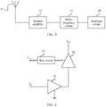
- FIG. IF is a schematic diagram of an application of a stacked amplifier in a radio frequency field according to an embodiment of this application.
- a radio frequency transceiver circuit 10 to which the stacked amplifier provided in this embodiment of this application is applied may include an antenna 11, a stacked amplifier 12, and a radio frequency circuit 13.
- the stacked amplifier 12 is connected between the antenna 11 and the radio frequency circuit 13, and may be configured to amplify a radio frequency signal transmitted between the antenna 11 and the radio frequency circuit 13, and then transmit the amplified radio frequency signal to a peer end.
- Signal transmission between the antenna 11 and the radio frequency circuit 13 is usually bidirectional, that is, the radio frequency transceiver circuit 10 may generally have a send path and a receive path.
- the radio frequency circuit 13 is integrated with a transmit end and a receive end.
- the send path is also referred to as a transmit path, and is a path for transmission from the transmit end on the radio frequency circuit 13 to the antenna 11.
- the receive path is a path for transmission from the antenna 11 to the receive end on the radio frequency circuit 13.
- the send path and the receive path share the same antenna 11. Therefore, when the send path is in an operating state, a receive end of the receive path may present a high-impedance state. On the contrary, when the receive path is in an operating state, a transmitter of the send path may present a high-impedance state.
- the stacked amplifier provided in the following embodiments may be disposed, so that the stacked amplifier has a high impedance in an off state based on different impedances of the stacked amplifier in different states. This implements a high impedance of a path in which the stacked amplifier is located, and the antenna is in an operating state on another path of the radio frequency transceiver circuit 10.
- the stacked amplifier 12 may be used on the send path of the radio frequency transceiver circuit 10, or may be used on the receive path of the radio frequency transceiver circuit 10, or may be used on both the send path and the receive path of the radio frequency transceiver circuit 10.
- the stacked amplifier 12 may also be referred to as a radio frequency amplifier, a radio frequency amplification circuit, or a power amplifier (Power Amplifier, PA).
- a radio frequency amplifier a radio frequency amplification circuit
- a power amplifier Power Amplifier, PA
- an input end of the stacked amplifier 12 may be connected to a send port of the radio frequency circuit 13, and an output end of the stacked amplifier 12 is connected to the antenna 11.
- the stacked amplifier 12 may also be referred to as a low noise amplifier (Low Noise Amplifier, LNA).
- LNA Low Noise Amplifier
- an input end of the stacked amplifier 12 may be connected to the antenna 11, and an output end of the stacked amplifier 12 is connected to a receive port of the radio frequency circuit 13.
- FIG. 2 is an example diagram of an application of the stacked amplifier in the radio frequency transceiver circuit according to an embodiment of this application.
- the radio frequency circuit 13 may have a send port TX and a receive port RX.
- An input end of the stacked amplifier 12 may be connected to the send port TX of the radio frequency circuit 13, to obtain, from the send port TX, a radio frequency input (RF in ) signal generated by the radio frequency circuit 13.
- An output end of the stacked amplifier 12 may be connected to an antenna 11, to transmit, by using the antenna 11, a radio frequency output (RF out ) signal obtained by amplifying the radio frequency input signal.
- different impedances in an on (ON) state and an off (OFF) state may be implemented by using the stacked amplifier 12 in the following embodiments of this application, so that the impedance of the stacked amplifier 12 in an off state is greater than a preset impedance, to implement a high impedance in an off state.
- the preset impedance may be greater than or equal to an impedance of the stacked amplifier in the on state.
- the antenna 11 On a receive path of the radio frequency transceiver circuit 10, the antenna 11 may be connected to the receive port RX of the radio frequency circuit 13 by using an inductor L.
- the receive port RX is further connected to a receive switch (Switch receive, SW RX).
- a changeover switch may be configured to implement a high impedance in an off state.
- radio frequency transceiver circuit 10 shown in FIG. IF or FIG. 2
- another circuit component may be further connected between the radio frequency circuit 13 and the antenna 11. This is not limited in this application.
- the stacked amplifier and the radio frequency transceiver circuit provided in technical solutions of this application may be used in any communication device that has a wireless communication function.
- the communication device may be a wireless network device such as a base station, or may be a wireless terminal device.
- the wireless terminal device in this application may be a device that provides a user with voice and/or data connectivity, a handheld device with a wireless connection function, or another processing device connected to a wireless modem.
- the wireless terminal device may communicate with one or more core networks through a radio access network (radio access network, RAN).
- radio access network radio access network
- the wireless terminal device may be a wireless mobile terminal, for example, a mobile phone (cellular phone) and a computer having a mobile terminal, or may be a portable, pocket-sized, handheld, computer built-in, or vehicle-mounted wireless mobile apparatus or a wireless Internet of Things device, for example, a personal communication service (Personal Communication Service, PCS) phone, a cordless phone, a session initiation protocol (Session Initiation Protocol, SIP) phone, a wireless local loop (Wireless Local Loop, WLL) station, or a personal digital assistant (Personal Digital Assistant, PDA), which exchanges voice and/or data with a radio access network.
- PCS Personal Communication Service
- SIP Session Initiation Protocol
- WLL Wireless Local Loop
- PDA Personal Digital Assistant
- the terminal may also be referred to as user equipment (User Equipment, UE), a mobile station (Mobile Station, MS), a mobile terminal (mobile terminal), a subscriber unit (Subscriber Unit, SU), a subscriber station (Subscriber Station, SS), a mobile station (Mobile Station, MB), a remote station (Remote Station, RS), an access point (Access Point, AP), a remote terminal (Remote Terminal, RT), an access terminal (Access Terminal, AT), or a user terminal (User Terminal, UT), a user agent (User Agent, UA), a terminal device (User Device, UD), user equipment (User Equipment, UE), or the like. This is not limited in this application.
- the base station may be a device that communicates with a terminal by using one or more sectors on an air interface in an access network, and may coordinate attribute management of the air interface.
- the radio access network device may be a base station in GSM or CDMA, for example, a base transceiver station (base transceiver station, BTS), or may be a base station in WCDMA, for example, a NodeB, or may be an evolved NodeB in LTE, for example, an eNB or an e-NodeB (evolutional NodeB), or may be a base station in a 5G system, for example, a transmission reception point (Transmission Reception Point, TRP) or a g-NodeB (g-NodeB, gNB), or a base station in a future network.
- TRP Transmission Reception Point
- g-NodeB g-NodeB
- gNB g-NodeB
- the base station may be a relay device, or another network element device having a
- FIG. 3 is a schematic diagram of a structure of a communication device according to an embodiment of this application.
- the communication device may further include a baseband circuit 20.
- the baseband circuit 20 may be connected to a radio frequency circuit 13 in the radio frequency transceiver circuit 10.
- the radio frequency circuit 13 may transform a baseband signal output by the baseband circuit 20 into a radio frequency input signal, and output the radio frequency input signal to the stacked amplifier 12, so that the stacked amplifier 12 amplifies the radio frequency input signal to obtain a radio frequency output signal, and transmits the radio frequency output signal by using an antenna 11.
- the radio frequency circuit 13 may further transmit a generated bias voltage to the stacked amplifier 12, so that the stacked amplifier 12 has different impedances under an effect of a bias voltage, and an impedance of the stacked amplifier 12 in an off state is greater than a preset impedance. This implements a high impedance of the stacked amplifier 12 in an off state, and therefore implements control over on/off switching of the stacked amplifier 12.
- a bias circuit in the stacked amplifier may be improved, so that the stacked amplifier has different impedances under an effect of a bias voltage and under an effect of different bias voltages, and an impedance in an off state is greater than a preset impedance. This implements a high impedance in an off state without a changeover switch, and reduces a bidirectional loss of a circuit, and improves bidirectional port performance of the circuit.
- the stacked amplifier is also referred to as a stacked transistor amplifier, and is an amplifier formed by stacking a plurality of layers of transistors.
- the stacking of transistors refers to that an output end of a previous layer of transistor is connected to an input end of a next layer of transistor, to input a signal amplified by the previous layer of transistor to the input end of the next layer of transistor, so that the signal is amplified by the next layer of transistor, and a voltage of the amplified signal output by the stacked amplifier is shared by the plurality of layers of amplifier.
- FIG. 4 is a diagram of a structure of a circuit of a stacked amplifier according to an embodiment of this application.
- the stacked amplifier may include a first transistor 41, a second transistor 42, and a bias circuit 43.
- a bias end of the first transistor 41 is grounded.
- An input end of the first transistor 41 is configured to receive an input signal.
- An output end of the first transistor 41 is connected to an input end of the second transistor 42.
- a bias end of the second transistor 42 is connected to a control output end of an external circuit through the bias circuit 43, to receive a bias voltage that is output by the external circuit through the control output end.
- An output end of the second transistor 42 is configured to output an amplified signal.
- the bias circuit 43 is configured to implement that, under an effect of different bias voltages, the second transistor 42 has different impedances, and an off impedance of the second transistor 42 is greater than a preset impedance.
- the off impedance is an impedance of the second transistor 42 under an effect of an off bias voltage.
- the preset impedance may be greater than or equal to an on impedance.
- the on impedance may be an impedance of the second transistor 42 under an effect of an on bias voltage.
- the external circuit may be, for example, a radio frequency circuit in the radio frequency field or another control circuit.
- the first transistor 41 may be a first layer of transistor of the stacked amplifier.
- the input end of the first transistor 41 is an input end of the stacked amplifier, and may be connected to a first external signal end, to receive an input signal from the first external signal end.
- the bias end of the first transistor 41 is grounded, so that the first transistor 41 can amplify the input signal.
- the input end of the second transistor 42 is connected to the output end of the first transistor 41, to obtain an amplified signal of the first transistor 41.
- the output end of the second transistor 42 is an output end of the stacked amplifier, and may be connected to a second external signal end, to output an output signal amplified by the second transistor 42, to the second external signal end.
- the bias end of the second transistor 42 is connected to the bias circuit 43.
- the bias circuit 43 may obtain the bias voltage from the control output end of the external circuit.
- the bias voltage may be an on bias voltage (V ON ), or an off bias voltage (V OFF ).
- the bias circuit 43 may implement an amplification function by using the second transistor 42 under an effect of the on bias voltage, to amplify the signal amplified by the first transistor 41 again.
- a signal voltage amplified by the stacked amplifier may be a sum of a voltage amplified by the first transistor 42 and a voltage amplified by the second transistor 42.
- the input end of the first transistor 41 may be connected to a radio frequency circuit in the radio frequency transceiver circuit.
- the radio frequency circuit may have a send port and a receive port.
- the input end of the first transistor 41 may be connected to the send port of the radio frequency circuit, to obtain a radio frequency input signal generated by the radio frequency circuit.
- the output end of the second transistor 41 may be connected to an antenna, to output a radio frequency output signal amplified by the second transistor 42 to the second external signal end.
- the first external signal end connected to the input end of the first transistor 41 may be the send port of the radio frequency circuit.
- the second external signal end connected to the output end of the second transistor 42 may be the antenna.
- the input end of the first transistor 41 may be connected to an antenna in the radio frequency transceiver circuit.
- the input end of the first transistor 41 may be connected to the antenna, to obtain a radio frequency input signal received by the antenna.
- the first external signal end connected to the input end of the first transistor 41 may be the antenna.
- the second external signal end connected to the output end of the second transistor 42 may be a receive port of a radio frequency circuit.
- the bias circuit 43 may be improved, so that the bias circuit 43 can implement that the second transistor 42 amplifies a signal under an effect of an on bias voltage, and adjust an impedance of the second transistor 42 under an effect of an off bias voltage if a bias voltage changes from the on bias voltage to the off bias voltage. Therefore, the second transistor 42 has different impedances in an on state and an off state. Due to improvement of the bias circuit 43, an off impedance of the second transistor 42 is greater than a preset impedance, that is, the off impedance of the second transistor 42 is increased. This implements a high impedance of the second transistor 42 in an off state, and therefore implements a high impedance of the stacked amplifier in an off state.
- the preset impedance may be greater than an on impedance.
- the on impedance may be an impedance of the second transistor 42 under an effect of an on bias voltage.
- the bias circuit 43 may include a bias resistor and a variable impedance device.
- the bias resistor and the variable impedance device may be connected in series between the control output end and the ground.
- the bias end of the second transistor 42 is connected between the bias resistor and the variable impedance device.
- each transistor may be a bipolar transistor (Bipolar Junction Transistor, BJT) or a field effect transistor (Field Effect Transistor, FET).
- BJT Bipolar Junction Transistor
- FET Field Effect Transistor
- the bipolar transistor may also be referred to as a semiconductor transistor, a crystal transistor, or another description, and may be an NPN-type transistor or a PNP-type transistor.
- the field effect transistor is also referred to as a unipolar transistor, and may be a junction field effect transistor (Junction Field Effect Transistor, JFET) or a metal oxide semiconductor field effect transistor (Metal-Oxide Semiconductor FET, MOS-FET).
- the second transistor 42 is an N-type MOS transistor or an NPN-type transistor
- an impedance of the variable impedance device is negatively correlated with the bias voltage, and the on bias voltage is greater than the off bias voltage.
- the impedance of the variable impedance device increases as the bias voltage decreases.
- a larger bias voltage indicates a smaller impedance of the variable impedance device, and a smaller bias voltage indicates a larger impedance of the variable impedance device.
- impedance of the second transistor 42 may be adjusted by using the variable impedance device in the bias circuit 43. Because the impedance of the variable impedance device is negatively correlated with the bias voltage, when the on bias voltage is greater than the off bias voltage, the off impedance of the second transistor 42 under an effect of the off bias voltage may be greater than the preset impedance. Therefore, the impedance of the second transistor 42 in an off state is increased.
- the second transistor 42 is a P-type MOS transistor or a PNP-type transistor
- an impedance of the variable impedance device is positively correlated with the bias voltage, and the on bias voltage is less than the off bias voltage.
- the impedance of the variable impedance device increases as the bias voltage increases.
- a larger bias voltage indicates a larger impedance of the variable impedance device, and a smaller bias voltage indicates a smaller impedance of the variable impedance device.
- the impedance of the second transistor 42 may be adjusted by using the variable impedance device in the bias circuit 43. Because the impedance of the variable impedance device is positively correlated with the bias voltage, when the on bias voltage is less than the off bias voltage, the off impedance of the second transistor 42 under an effect of the off bias voltage may be greater than the preset impedance. This implements the high impedance of the second transistor 42 in an off state.
- variable impedance device shown in any one of the foregoing may be, for example, a variable capacitive device.
- a capacitance of the variable capacitive device may be adjusted, so that the capacitance of the variable capacitive device decreases under the effect of the off bias voltage. Therefore, the impedance of the second transistor 42 in an off state is increased.
- variable impedance device shown in any one of the foregoing may also be, for example, a variable inductive device.
- An inductance of the variable inductive device may be adjusted, so that the inductance of the variable inductive device increases under the effect of the off bias voltage. Therefore, the impedance of the second transistor 42 in an off state is increased.
- the preset impedance mentioned above may be, for example, an off impedance under the effect of the off bias voltage, that is, a preset fixed off impedance, when a fixed impedance device is disposed in the bias circuit 43.
- the input end of the first transistor may receive the input signal
- the output end of the first transistor is connected to the input end of the second transistor
- the bias end of the first transistor is grounded, so that the first transistor can amplify the input signal.
- the bias end of the second transistor may be connected to the control output end of the external circuit through the bias circuit, to receive the bias voltage output by the external circuit through the control output end. Because the bias circuit includes the bias resistor and the variable impedance device, the second transistor can amplify, under the effect of the on bias voltage, the signal output by the first transistor, and the impedance of the second transistor in an off state is greater than the preset impedance.
- the stacked amplifier may amplify the signal by using the first transistor and the second transistor, and may further implement, by using the variable impedance device in the bias circuit of the second transistor, that the impedance of the second transistor in an off state is greater than the preset impedance.
- This implements the high impedance of the second transistor in an off state, to implement the high impedance of the stacked amplifier in an off state. Therefore, on/off state switching of the stacked amplifier can be implemented without an additional changeover switch, and a loss of a circuit is reduced, to ensure bidirectional port performance of the circuit for the high-frequency signal.
- variable impedance device in the bias circuit of the second transistor in the stacked amplifier may implement the high impedance of the stacked amplifier in an off state of the high-frequency signal, and avoid a leakage current of a path on which the stacked amplifier is located in an off state. This reduces the loss of the circuit, and ensures bidirectional port performance of the circuit for the high-frequency signal.
- FIG. 5 is a diagram of a structure of a circuit of another stacked amplifier according to an embodiment of this application.
- the bias circuit 43 may include a bias resistor R 1 and a variable capacitive device C 1 .
- the bias resistor R 1 and the variable capacitive device C 1 are connected in series between a control output end and the ground.
- a bias end of the second transistor 42 is connected between the bias resistor R 1 and the variable capacitive device C 1 .
- the control output end is the control output end of the external circuit mentioned above.
- the control output end may be configured to output a bias voltage V cas .
- the variable capacitive device C 1 may be implemented in an analog manner, and may be a varactor (Varactor) or a metal-oxide-semiconductor (metal-oxide-semiconductor, MOS) capacitor.
- the variable capacitive device C 1 may also be implemented in a numerical control manner, for example, implemented by using a switched capacitor, that is, a combination of a switch component and a fixed capacitor.
- the bias voltage V cas may be an on voltage V ON , also referred to as an on bias voltage, or may be an off voltage V OFF , also referred to as an off bias voltage.
- the bias resistor R 1 and the variable capacitive device C 1 are connected in series between the control output end and the ground. Under an effect of the on bias voltage, a capacitance value of the variable capacitive device C 1 may be an on capacitance value C ON , so that an on impedance of the second transistor 42 is r ON , and the second transistor 42 is in an amplifying state, to amplify a signal.
- a capacitance value of the variable capacitive device C 1 may be an off capacitance value C OFF , so that an off impedance of the second transistor 42 is r OFF , and the second transistor 42 is in an off state.
- the second transistor 42 is an N-type MOS transistor or an NPN-type transistor, and the on bias voltage is greater than the off bias voltage, the on capacitance C ON under the effect of the on bias voltage is greater than the off capacitance C OFF under the effect of the off bias voltage, so that the on impedance r ON of the second transistor 42 is less than the off impedance r OFF of the second transistor 42, to increase the on impedance of the second transistor 42.
- the MOS capacitor shown above may be an N-type MOS capacitor, or may be a P-type MOS capacitor.
- the following first describes a connection relationship of the variable capacitive device in the stacked amplifier provided in this embodiment of this application by using an N-type MOS capacitor as an example.
- FIG. 5A is a schematic diagram of the stacked amplifier whose variable capacitive device is an N-type MOS capacitor according to an embodiment of this application.
- the variable capacitive device C 1 may be an N-type MOS capacitor.
- a gate of the N-type MOS capacitor is connected between the bias resistor R 1 and the bias end of the second transistor 42.
- a source, a drain, and a substrate of the N-type MOS capacitor are all grounded.
- FIG. 5B is another schematic diagram of the stacked amplifier whose variable capacitive device is an N-type MOS capacitor according to an embodiment of this application.
- the variable capacitive device C 1 may be an N-type MOS capacitor.
- a gate of the N-type MOS capacitor is connected between the bias resistor R 1 and the bias end of the second transistor 42. Both a source and a drain of the N-type MOS capacitor are grounded.
- a substrate of the N-type MOS capacitor is grounded by using a preset resistor.
- FIG. 5C is still another schematic diagram of the stacked amplifier whose variable capacitive device is an N-type MOS capacitor according to an embodiment of this application.
- the variable capacitive device C 1 may be an N-type MOS capacitor.
- a gate of the N-type MOS capacitor is connected between the bias resistor R 1 and the bias end of the second transistor 42. Both a drain and a substrate of the N-type MOS capacitor are grounded.
- a source of the N-type MOS capacitor is grounded by using a preset resistor.
- variable capacitive device may alternatively be the P-type MOS capacitor.
- a gate of the P-type MOS capacitor is grounded.
- a source, a drain, and a substrate of the P-type MOS capacitor are all grounded and connected between the bias resistor R 1 and the bias end of the second transistor 42.
- a gate of the P-type MOS capacitor is grounded. Both a source and a drain of the P-type MOS capacitor are connected between the bias resistor R 1 and the bias end of the second transistor 42. A substrate of the P-type MOS capacitor is connected between the bias resistor R 1 and the bias end of the second transistor 42 by using a preset resistor.
- a gate of the P-type MOS capacitor is grounded. Both a source and a substrate of the P-type MOS capacitor are connected between the bias resistor R 1 and the bias end of the second transistor 42. A drain of the P-type MOS capacitor is connected between the bias resistor R 1 and the bias end of the second transistor 42 by using a preset resistor.
- connection manner of the N-type MOS capacitor or the P-type MOS capacitor in the stacked amplifier is not limited to the foregoing example, and may be another manner. Details are not described herein.
- the off impedance of the second transistor may be greater than the preset impedance by using the variable capacitive device in the bias circuit.
- This implements a high impedance of the second transistor in an off state, and therefore implements a high impedance of the stacked amplifier in an off state. Therefore, on/off state switching of the stacked amplifier can be implemented without an additional changeover switch.
- the impedance of the second transistor in an off state is increased by using the variable capacitive device, so that a circuit is simpler in structure, lower in loss cost, and easier to implement.
- the stacked amplifier shown in any one of the foregoing in this application may be used in a single-ended structure, or may be used in a differential structure, that is, a dual-ended structure.
- the following uses a stacked amplifier with a differential structure as an example for description.
- the stacked amplifier with the differential structure is also referred to as a differential amplifier.
- FIG. 6 is a schematic diagram of a stacked amplifier with a differential structure according to an embodiment of this application.
- the stacked amplifier with the differential structure may include two single-ended amplifiers.
- Each single-ended amplifier may be similar to the stacked amplifier shown in any one of FIG. 4 or FIG. 5 , and may include a first transistor 41, a second transistor 42, and a bias circuit 43.
- Differential input ends of the stacked amplifier with the differential structure may be input ends of the first transistors 41 in the two single-ended amplifiers. Both the input ends may receive the input signal. Bias ends of the first transistors 42 in the two single-ended amplifiers are both grounded. Output ends of the first transistors 41 in the two single-ended amplifiers are separately connected to an input end of one second transistor 42.
- Differential output ends of the stacked amplifier with the differential structure may be output ends of the second transistors 42 in the two single-ended amplifiers. Both the output ends may output the amplified signal. Bias ends of the second transistors 42 in the two single-ended amplifiers are separately connected to a control output end through one bias circuit 43, to obtain a bias voltage output by the control output end.
- the stacked amplifier with the differential structure provided in this embodiment includes two single-ended amplifiers.
- Each single-ended amplifier may be similar to any one of the foregoing stacked amplifiers, that is, include a first transistor 41, a second transistor 42, and a bias circuit 43.
- a connection relationship between the first transistor 41, the second transistor 42, and the bias circuit 43 in each single-ended amplifier may be similar to the foregoing connection relationship.
- Each bias circuit 43 is connected to a control output end, that is, the bias circuits 43 have a same bias voltage.
- the stacked amplifier provided in this embodiment of this application is used in a differential structure, so that a high impedance of each stacked amplifier in an off state may be implemented, based on differential amplification. Therefore, on/off switching is implemented without using an additional changeover switch, and a loss of a circuit is reduced, to ensure a performance advantage of the circuit for a high-frequency signal.
- the stacked amplifier shown in any one of the foregoing descriptions may be implemented by being integrated into a chip, or may be implemented as a discrete component, or may allow stacking of more stages. That is, the stacked amplifier shown in any one of the foregoing may include: a plurality of stages of second transistors 42 and a plurality of bias circuits 43.
- FIG. 7 is a schematic diagram of a multi-stage stacked amplifier according to an embodiment of this application. As shown in FIG. 7 , the multi-stage stacked amplifier includes a first transistor 41 and a plurality of stages of second transistors 42. Connection of each port of the first transistor may be similar to that of the first transistor 41 in any one of the foregoing stacking methods. Details are not described herein again.
- an input end of a first stage of second transistor 42 is connected to an output end of the first transistor 41.
- An input end of a back stage of second transistor 42 is connected to an output end of a front stage of second transistor 42.
- a bias end of each stage of second transistor 42 is connected to a control output end through one bias circuit 43.
- the bias circuits 43 of the plurality of stages of second transistors 42 may share one bias voltage, that is, all the bias circuits 43 are connected to the control output end of an external circuit to obtain the bias voltage, so that each stage of second transistor 42 may amplify a signal under an effect of an on bias voltage.
- an output end of a last stage of second transistor 42 may be an output end of the stacked amplifier, to output an amplified signal.
- the multi-stage stacked amplifier provided in this embodiment, multiple amplifications may be performed by using a plurality of stages of second transistors, so that an amplification gain of a signal may be ensured.
- the stacked amplifier may be used for multi-stage stacking. If multi-stage amplification is implemented through multi-stage stacking, a high impedance in an off state may be implemented. Therefore, on/off switching is implemented without using an additional changeover switch, and a loss of a circuit is reduced, to ensure bidirectional port performance of the circuit for a high-frequency signal.
- each transistor may be a bipolar transistor or a field-effect transistor.
- FIG. 8 is a schematic diagram of a stacked amplifier using an N-type MOS transistor according to an embodiment of this application.
- the stacked amplifier may be an amplifier of a cascode (cascode) structure.
- the first transistor 41 may be a common-source (Common Source) transistor, and may be, for example, a first MOS transistor M 1 shown in FIG. 8 .
- the second transistor 42 may be a common-gate transistor, and may be, for example, a second MOS transistor M 2 shown in FIG. 8 .
- the bias circuit 43 is described by using a circuit structure similar to that in FIG. 5 as an example.
- the bias circuit 43 provided in this embodiment of this application may be of another circuit structure, for example, any structure shown in FIG. 5A , FIG. 5B, or FIG. 5C . This is not limited in this application.
- a gate of the first MOS transistor M 1 may serve as an input end of the first transistor 41, to receive an input signal.
- a drain of the first MOS transistor M 1 may serve as an output end of the first transistor 41, to output an amplified signal of the first transistor 41.
- a source of the first MOS transistor M 1 may serve as a bias end of the first transistor 41, and is grounded to provide a bias for the first MOS transistor M 1 , so that the first MOS transistor M 1 may be in a saturation area, to reversely implement a signal.
- a source of the second MOS transistor M 2 may serve as an input end of the second transistor 42, to receive the signal output by the first transistor 41.
- a drain of the second MOS transistor M 2 may serve as an output end of the second transistor 42, to output the amplified signal of the second transistor 42.
- a gate of the second MOS transistor M 2 may serve as a bias end of the second transistor 42, and is connected to the bias circuit 43.
- a bias resistor R 1 and a variable capacitive device C 1 may implement that, under an effect of an on bias voltage, the second MOS transistor M 2 is also in a saturation area, to forwardly amplify a signal. In this way, a voltage of the amplified signal output by the stacked amplifier may be shared by the first MOS transistor M 1 and the second MOS transistor M 2 .
- a capacitance value of the variable capacitive device C 1 in the bias circuit 43 under an effect of an on bias voltage is an on capacitance C ON
- a capacitance value of the variable capacitive device C 1 under an effect of an off bias voltage is an off capacitance C OFF . If the on bias voltage is greater than the off bias voltage, the off capacitance C OFF of the second MOS transistor M 2 may be less than the on capacitance C ON , so that an off impedance of the second MOS transistor M 2 is increased.
- FIG. 9 is a schematic diagram of a stacked amplifier using an NPN transistor according to an embodiment of this application.
- the first transistor 41 may be a common-emitter (Common Emitter) transistor, and may be, for example, a first triode Q 1 shown in FIG. 9 .
- the second transistor 42 may be a common-base transistor, and may be, for example, a second triode Q 2 shown in FIG. 9 .
- the bias circuit 43 is described by using a circuit structure similar to that in FIG. 5 as an example.
- the bias circuit 43 provided in this embodiment of this application may be of another circuit structure, for example, any structure shown in FIG. 5A , FIG. 5B, or FIG. 5C . This is not limited in this application.
- a base of the first triode Q 1 may serve as an input end of the first transistor 41, to receive an input signal.
- a collector of the first triode Q 1 may serve as an output end of the first transistor 41, to output the amplified signal of the first transistor 41.
- An emitter of the first triode Q 1 may serve as a bias end of the first transistor 41 and is grounded, so that the first triode Q 1 may be in an amplification area, to reversely amplify a signal.
- An emitter of the second triode Q 2 may serve as an input end of the second transistor 42, to receive the signal output by the first transistor 41.
- a collector of the second triode Q 2 may serve as an output end of the second transistor 42, to output the amplified signal of the second transistor 42.
- a base of the second triode Q 2 may serve as a bias end of the second transistor 42, and is connected to the bias circuit 43.
- a bias resistor R 1 and a variable capacitive device C 1 may implement that, under an effect of an on bias voltage, the second triode Q 2 is also in the amplification area, to forwardly amplify a signal. In this way, a voltage of the amplified signal output by the stacked amplifier may be shared by the first triode Q 1 and the second triode Q 2 .
- a capacitance value of the variable capacitive device C 1 in the bias circuit 43 under an effect of an on bias voltage is an on capacitance C ON
- a capacitance value of the variable capacitive device C 1 under an effect of an off bias voltage is an off capacitance C OFF . If the on bias voltage is greater than the off bias voltage, the off capacitance C OFF of the second triode Q 2 may be less than the on capacitance C ON , so that an off impedance of the second triode Q 2 is increased.
- FIG. 8 and FIG. 9 show possible implementations in which two different types of transistors are used.
- each transistor may alternatively be another transistor, and this is not limited to the foregoing. This is not limited in this embodiment of this application.
- the stacked amplifier provided in this embodiment of this application may further include a transformer.
- the transformer may also be referred to as an output transformer, and is configured to transform the amplified signal output by the stacked amplifier and then output the transformed signal.
- a primary coil of the transformer is connected to an output end of the second transistor 42.
- the transformer is configured to transform the amplified signal, and then output the transformed signal through an output end of a secondary coil.
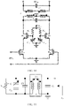
- FIG. 10 is a schematic diagram of another stacked amplifier with a differential structure according to an embodiment of this application. As shown in FIG. 10 , the stacked amplifier with the differential structure may include: two first MOS transistors, two second MOS transistors, a transformer T 1 , a second capacitor C 2 , a third capacitor C 3 , and two bias circuits.
- a first a transistor M 1a and a first b transistor M 1b may serve as input transistors of the stacked transistors. Gates of the first a transistor M 1a and the first b transistor M 1b may receive a radio frequency input (RF in ) signal. Sources of the first a transistor M 1a and the first b transistor M 1b are both grounded. A drain of the first a transistor M 1a is connected to a source of a second a transistor M 2a . A drain of the first b transistor M 1b is connected to a source of a second b transistor M 2b .
- the second a transistor M 2a and the second b transistor M 2b may be common-gate transistors in the stacked transistors.
- the two bias circuits are respectively bias circuits of two second MOS transistors.
- a first a bias resistor R 1a and a first a variable capacitive device C 1a form a bias circuit of the second a transistor M 2a .
- a first b bias resistor R 1b and a first b variable capacitive device C 1b form a bias circuit of the second b transistor M 2b .
- the two bias circuits are both connected between a control output end of an external circuit and the ground.
- a gate of the second a transistor M 2a is connected between the first a bias resistor R 1a and the first a variable capacitive device C 1a .
- a gate of the second b transistor M 2b is connected between the first b bias resistor R 1b and the first b variable capacitive device C 1b .
- the first a variable capacitive device C 1a and the first b variable capacitive device C 1b are respectively alternating-current ground capacitors of the second a transistor M 2a and the second b transistor M 2b .
- the transformer T 1 is the output transformer of the stacked transistor.
- the second capacitor C 2 is a coordinated capacitor connected to the primary coil of the transformer T 1 .
- the third capacitor C 3 is a coordinated capacitor connected to the secondary coil of the transformer T 1 .
- An output end of the secondary coil of the transformer T 1 is an output end of the stacked amplifier, to output a radio frequency output (RF out ) signal
- FIG. 11 is an equivalent circuit diagram of another stacked amplifier with a differential structure in an off state according to an embodiment of this application.
- a gate-drain capacitance C2' in FIG. 11 is a sum of gate-drain capacitances (C gd ) of the second capacitor C 2 , the second a transistor M 2a , and the second b transistor M 2b in FIG. 10 .
- a gate-source capacitance C gs2 is a sum of gate-source capacitances (C gs ) of the second a transistor M 2a and the second b transistor M 2b .
- the alternating-current ground capacitors C 1 are the first a variable capacitive device C 1a and the first b variable capacitive device C 1b in FIG. 10 .
- An impedance ro is a real part of an output impedance of the second a transistor M 2a and the second b transistor M 2b .
- FIG. 12 is a curve diagram of a change between a bias voltage and a capacitance value of an alternating-current ground capacitor of the another stacked amplifier with the differential structure according to an embodiment of this application.
- both the first a variable capacitive device C 1a and the first b variable capacitive device C 1b are variable capacitive devices, so that when the bias voltage V cas is an on bias voltage, also referred to as an on voltage V ON , that is, a preset high voltage, the stacked amplifier is in an on state, and the alternating-current ground capacitor C 1 presents a preset on capacitance value C ON .
- the bias voltage is an off bias voltage, also referred to as an off voltage V OFF , that is, a preset low voltage
- the stacked amplifier is in an off state
- the alternating-current ground capacitor C 1 presents a preset off capacitance value C OFF .
- FIG. 13 is a curve diagram of a change between a signal frequency and a capacitance value of an alternating-current ground capacitor of the second MOS transistor in the another stacked amplifier with the differential structure according to an embodiment of this application. It can be learned from FIG. 13 that, as the signal frequency increases, a difference between the on capacitance C ON and the off capacitance C OFF of the alternating-current ground capacitor C 1 becomes larger. For a high-frequency signal, a capacitance value of the alternating-current ground capacitor C 1 of the stacked amplifier in an off state is reduced.
- the alternating-current ground capacitor C 1 presents different capacitance values in the on state and an off state, so that the impedance ro presents different impedances and is presented as a variable impedance. Because of an impedance transformation function of the transformer T 1 , the transformer T 1 presents different impedances in a preset frequency band. This implements a high impedance of the alternating-current ground capacitor C 1 in an off state under the high-frequency signal.
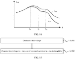
- FIG. 14 is a curve diagram of a change between a signal frequency and an impedance of the second MOS transistor in the another stacked amplifier with the differential structure according to an embodiment of this application. It can be learned from FIG.
- an on impedance r ON of the impedance ro is less than an off impedance r OFF .
- a difference between the on impedance r ON and the off impedance r OFF becomes larger.
- FIG. 15 is a schematic flowchart of a switching control method according to an embodiment of this application. As shown in FIG. 15 , the method may include the following steps.
- the bias voltage may be used to implement that, under an effect of different bias voltages, the second transistor has different impedances, and an off impedance of the second transistor is greater than a preset impedance.
- the off impedance is an impedance of the second transistor under an effect of an off bias voltage.
- the preset impedance may be greater than an on impedance.
- the on impedance may be an impedance of the second transistor under an effect of an on bias voltage.
- the preset impedance may be a preset off impedance, that is, an impedance of a fixed impedance device in the bias circuit of the second amplifier under an effect of the off bias voltage.
- the bias voltage may be generated by an external circuit.
- the bias voltage may be output to the bias end of the second transistor in the stacked amplifier through a control output end of the external circuit.
- the bias circuit implements that, under an effect of different bias voltages, the second transistor has different impedances, and the off impedance of the second transistor is greater than the preset impedance.
- the bias voltage may be generated, and the bias voltage may be output to the stacked amplifier, so that the stacked amplifier presents different impedances under an effect of different bias voltages, to implement a high impedance in an off state, so as to implement on/off state switching. Therefore, on/off state switching of the stacked amplifier can be implemented without an additional changeover switch, a loss of a circuit is reduced, and a leakage current of a path in which the stacked amplifier is located in an off state can be avoided. The loss of the circuit is further reduced, to effectively ensure bidirectional port performance of the circuit for the high-frequency signal.
- connection in the foregoing embodiments of this application may be a direct connection or an indirect connection.
- the direct connection may be, for example, a direct contact connection or a connection by using a wire.
- the indirect connection may be, for example, a coupling connection or a connection by using another element.
- a specific form of the connection is not limited in this embodiment of this application.
Landscapes
- Engineering & Computer Science (AREA)
- Power Engineering (AREA)
- Microelectronics & Electronic Packaging (AREA)
- Amplifiers (AREA)
- Transceivers (AREA)
Abstract
Description
- This application relates to electronic technologies, and in particular, to a stacked amplifier, a radio frequency transceiver circuit, a device, and a switching control method.
- In an electronic control application, to facilitate subsequent signal transmission or processing, an amplifier usually needs to be disposed to amplify a signal.
- To ensure a signal amplification effect, a stacked amplifier with a plurality of amplifiers may be configured to amplify a signal. Currently, an impedance of a transistor in a stacked amplifier is generally fixed, and consequently an off (OFF) impedance cannot meet a requirement. Therefore, if a circuit in which the stacked amplifier is located requires state switching, a switch component needs to be additionally disposed to perform state switching.
- However, the additional switch component is disposed to perform state switching, a large loss of the circuit is caused, and performance of the circuit for a high-frequency signal is greatly reduced.
- Embodiments of this application provide a stacked amplifier, a radio frequency transceiver circuit, a device, and a switching control method, to reduce a loss of a circuit and improve performance of the circuit for a high-frequency signal.
- According to a first aspect, an embodiment of this application provides a stacked amplifier, including a first transistor, a second transistor, and a bias circuit.
- A bias end of the first transistor is grounded. An input end of the first transistor is configured to receive an input signal. An output end of the first transistor is connected to an input end of the second transistor.
- A bias end of the second transistor is connected to a control output end of an external circuit through the bias circuit, to receive a bias voltage that is output by the external circuit through the control output end. An output end of the second transistor is configured to output an amplified signal. The bias circuit is configured to implement that, under an effect of different bias voltages, the second transistor has different impedances, and an off impedance of the second transistor is greater than a preset impedance. The off impedance is an impedance of the second transistor under an effect of an off bias voltage.
- In a possible implementation, the bias circuit includes a bias resistor and a variable impedance device. The bias resistor and the variable impedance device are connected in series between the control output end and the ground. The bias end of the second transistor is connected between the bias resistor and the variable impedance device.
- According to a second aspect, an embodiment of this application further provides a stacked amplifier, including a first transistor, a second transistor, and a bias circuit.
- A bias end of the first transistor is grounded. An input end of the first transistor is configured to receive an input signal. An output end of the first transistor is connected to an input end of the second transistor.
- A bias end of the second transistor is connected to a control output end of an external circuit through the bias circuit, to receive a bias voltage that is output by the external circuit through the control output end. An output end of the second transistor is configured to output an amplified signal. The bias circuit includes a bias resistor and a variable impedance device. The bias resistor and the variable impedance device are connected in series between the control output end and the ground. The bias end of the second transistor is connected between the bias resistor and the variable impedance device.
- In a possible implementation of the first aspect or the second aspect, the variable impedance device is a variable capacitive device.
- According to the stacked amplifier provided in this solution, an off impedance of the second transistor may be greater than a preset impedance by using the variable capacitive device in the bias circuit, so that an impedance of the second transistor in an off state is increased. This implements a high impedance of the second transistor in an off state, and therefore implements a high impedance of the stacked amplifier in an off state. The impedance of the second transistor in an off state is increased by using the variable capacitive device, so that a circuit is simpler in structure, lower in loss cost, and easier to implement.
- In another possible implementation, the variable impedance device may further be a variable inductive device.
- In still another possible implementation, the variable capacitive device is a metal oxide semiconductor MOS capacitor.
- In yet still another possible implementation, the MOS capacitor may be an N-type MOS capacitor.
- In yet still another possible implementation, a gate of the N-type MOS capacitor is connected to the bias resistor. A source, a drain, and a substrate of the N-type MOS capacitor are all grounded.
- In yet still another possible implementation, a gate of the N-type MOS capacitor is connected to the bias resistor. Both a source and a drain of the N-type MOS capacitor are grounded. A substrate of the N-type MOS capacitor is grounded by using a preset resistor.
- In yet still another possible implementation, a gate of the N-type MOS capacitor is connected to the bias resistor. Both a drain and a substrate of the N-type MOS capacitor are grounded. A source of the N-type MOS capacitor is grounded by using a preset resistor.
- In yet still another possible implementation, the variable capacitive device shown above may also be a varactor or a switched capacitor.
- In still another possible implementation, the stacked amplifier is a differential amplifier. The differential amplifier includes two single-ended amplifiers. Each single-ended amplifier includes the first transistor, the second transistor, and the bias circuit.
- A differential input end of the differential amplifier is the input end of the first transistor in each of the two single-ended amplifiers. A differential output end of the differential amplifier is the output end of the second transistor in each of the two single-ended amplifiers.
- The stacked amplifier may be used in a differential structure, and may be a differential amplifier, so that a high impedance of each stacked amplifier in an off state may be implemented, based on differential amplification. Therefore, on/off switching is implemented without using an additional changeover switch, and a loss of a circuit is reduced, to ensure a performance advantage of the circuit for a high-frequency signal.
- In yet still another possible implementation, the stacked amplifier includes: a plurality of stages of second transistors and a plurality of bias circuits. In the plurality of stages of second transistors, an input end of a first stage of second transistor is connected to the output end of the first transistor. An input end of a back stage of second transistor is connected to an output end of a front stage of second transistor.
- A bias end of each stage of second transistor is connected to the control output end through one bias circuit.
- In a multi-stage stacked amplifier, multiple amplifications may be performed by using a plurality of stages of second transistors, so that an amplification gain of a signal may be ensured. In this embodiment, the stacked amplifier may be used for multi-stage stacking. If multi-stage amplification is implemented through multi-stage stacking, a high impedance in an off state may be implemented. Therefore, on/off switching is implemented without using an additional changeover switch, and a loss of a circuit is reduced, to ensure bidirectional port performance of the circuit for a high-frequency signal.
- In yet still another possible implementation, the stacked amplifier is a cascode amplifier. The first transistor is a common-source transistor. The first transistor is a common-source transistor. The input end of the first transistor is a gate of the common-source transistor. The output end of the first transistor is a drain of the common-source transistor. The bias end of the first transistor is a source of the common-source transistor.
- The second transistor is a common-gate transistor. The input end of the second transistor is a source of the common-gate transistor. The output end of the second transistor is a drain of the common-gate transistor. The bias end of the second transistor is a gate of the common-gate transistor.
- In yet still another possible implementation, the input end of the first transistor is a base of a common-emitter transistor. The output end of the first transistor is a collector of the common-emitter transistor. The bias end of the first transistor is an emitter of the common-emitter transistor.
- The input end of the second transistor is an emitter of a common-base transistor. The output end of the second transistor is a collector of the common-base transistor. The bias end of the second transistor is a base of the common-base transistor.
- In yet still another possible implementation, the stacked amplifier further includes a transformer. A primary coil of the transformer is connected to the output end of the second transistor. The transformer is configured to transform the amplified signal, and then output the transformed signal through an output end of a secondary coil.
- According to a third aspect, an embodiment of this application may further provide a radio frequency transceiver circuit, including: an antenna, a radio frequency circuit, and the stacked amplifier according to any one of the first aspect or the second aspect. The stacked amplifier is connected between the antenna and the radio frequency circuit.
- In a possible implementation, the stacked amplifier includes a first stacked amplifier. An input end of a first transistor in the first stacked amplifier is connected to the radio frequency circuit. An output end of a second transistor in the first stacked amplifier is connected to the antenna.
- In another possible implementation, the stacked amplifier further includes a second stacked amplifier. An input end of a first transistor in the second stacked amplifier is connected to the antenna. An output end of a second transistor in the second stacked amplifier is connected to the radio frequency circuit.
- According to a fourth aspect, an embodiment of this application further provides a communication device, including a baseband circuit and the radio frequency transceiver circuit according to any implementation of the third aspect. The baseband circuit is connected to a radio frequency circuit in the radio frequency transceiver circuit.
- According to a fifth aspect, an embodiment of this application further provides a switching control method, including:
- generating a bias voltage; and
- outputting a bias voltage to a bias end of a second transistor in the stacked amplifier according to any one of the first aspect or the second aspect, to implement that, under an effect of different bias voltages, the second transistor has different impedances, and an off impedance of the second transistor is greater than a preset impedance. The off impedance is an impedance of the second transistor under an effect of an off bias voltage.
- Embodiments of this application provide a stacked amplifier, a radio frequency transceiver circuit, a device, and a switching control method. The stacked amplifier may include a first transistor, a second transistor, and a bias circuit. A bias end of the first transistor is grounded. An input end of the first transistor is configured to receive an input signal. An output end of the first transistor is connected to an input end of the second transistor. A bias end of the second transistor is connected to a control output end of an external circuit through the bias circuit, to receive a bias voltage that is output by the external circuit through the control output end. An output end of the second transistor is configured to output an amplified signal. The bias circuit includes a bias resistor and a variable impedance device. The bias resistor and the variable impedance device are connected in series between the control output end and the ground. The bias end of the second transistor is connected between the bias resistor and the variable impedance device. In this application, the bias circuit connected to the bias end of the second transistor in the stacked amplifier may be improved, so that the bias circuit of the second transistor includes a variable impedance device. Through the bias circuit including the variable impedance device, the second transistor has different impedances under an effect of different bias voltages, and an impedance in an off state is greater than a preset impedance. This implements a high impedance of the second transistor in an off state, and therefore implements a high impedance of the stacked amplifier in an off state. Therefore, on/off state switching of the stacked amplifier can be implemented without an additional changeover switch, and a loss of a circuit is reduced, to ensure bidirectional port performance of the circuit.
-
-
FIG. 1A is a schematic diagram of an application example 1 of a stacked amplifier according to an embodiment of this application; -
FIG. 1B is a schematic diagram of an application example 2 of a stacked amplifier according to an embodiment of this application; -
FIG. 1C is a schematic diagram of an application example 3 of a stacked amplifier according to an embodiment of this application; - FIG. ID is a schematic diagram of a signal flow and a high-impedance state of a stacked amplifier in the application example 3 according to an embodiment of this application;
- FIG. IE is another schematic diagram of a signal flow and a high-impedance state of a stacked amplifier in the application example 3 according to an embodiment of this application;
- FIG. IF is a schematic diagram of an application of a stacked amplifier in a radio frequency field according to an embodiment of this application;
-
FIG. 2 is an example diagram of an application of a stacked amplifier in a radio frequency transceiver circuit according to an embodiment of this application; -
FIG. 3 is a schematic diagram of a structure of a communication device according to an embodiment of this application; -
FIG. 4 is a diagram of a structure of a circuit of a stacked amplifier according to an embodiment of this application; -
FIG. 5 is a diagram of a structure of a circuit of another stacked amplifier according to an embodiment of this application; -
FIG. 5A is a schematic diagram of a stacked amplifier whose variable capacitive device is an N-type MOS capacitor according to an embodiment of this application; -
FIG. 5B is another schematic diagram of a stacked amplifier whose variable capacitive device is an N-type MOS capacitor according to an embodiment of this application; -
FIG. 5C is still another schematic diagram of a stacked amplifier whose variable capacitive device is an N-type MOS capacitor according to an embodiment of this application; -
FIG. 6 is a schematic diagram of a stacked amplifier with a differential structure according to an embodiment of this application; -
FIG. 7 is a schematic diagram of a multi-stage stacked amplifier according to an embodiment of this application; -
FIG. 8 is a schematic diagram of a stacked amplifier using an N-type MOS transistor according to an embodiment of this application; -
FIG. 9 is a schematic diagram of a stacked amplifier using an NPN transistor according to an embodiment of this application; -
FIG. 10 is a schematic diagram of another stacked amplifier with a differential structure according to an embodiment of this application; -
FIG. 11 is an equivalent circuit diagram of another stacked amplifier with a differential structure in an off state according to an embodiment of this application; -
FIG. 12 is a curve diagram of a change between a bias voltage and a capacitance value of an alternating-current ground capacitor of another stacked amplifier with a differential structure according to an embodiment of this application; -
FIG. 13 is a curve diagram of a change between a signal frequency and a capacitance value of an alternating-current ground capacitor of a second MOS transistor in another stacked amplifier with a differential structure according to an embodiment of this application; -
FIG. 14 is a curve diagram of a change between a signal frequency and an impedance of a second MOS transistor in another stacked amplifier with a differential structure according to an embodiment of this application; and -
FIG. 15 is a schematic flowchart of a switching control method according to an embodiment of this application. - A stacked amplifier (Stacked Amplifier) provided in the following embodiments of this application may be used in any type of signal processing circuit. The signal processing circuit may be an independent processing chip, or may be a circuit module on another chip. The stacked amplifier may be configured to amplify an input signal, and then output the amplified signal.
- The stacked amplifier may be used in a bidirectional transmit/receive scenario. The following describes some implementations in the bidirectional transmit/receive scenario by using examples with reference to the accompanying drawings.
FIG. 1A is a schematic diagram of an application example 1 of a stacked amplifier according to an embodiment of this application.FIG. 1B is a schematic diagram of an application example 2 of a stacked amplifier according to an embodiment of this application. As shown inFIG. 1A , in an application example of a transmit/receive link in the bidirectional transmit/receive scenario, a firststacked amplifier 1 and a secondstacked amplifier 2 each have one side that may be connected to a bidirectional external interface, and the other side that may be connected to a unidirectional external interface. The bidirectional external interface may include an antenna interface. The bidirectional external interface connected to an input end of the firststacked amplifier 1 may be an antenna interface. The firststacked amplifier 1 is connected to an antenna through the antenna interface, to receive a signal received by the antenna, so as to amplify the signal received by the antenna. The external interface connected to an output side of the secondstacked amplifier 2 may be an antenna interface. The secondstacked amplifier 2 may be connected to the antenna through the antenna interface, to send an amplified signal to the antenna. - As shown in
FIG. 1B , in another application example of the transmit/receive link in the bidirectional transmit/receive scenario, the firststacked amplifier 1 and the secondstacked amplifier 2 each have one side that may be connected to a bidirectional external interface, and the other side that may be connected to a unidirectional external interface. The bidirectional external interface may include an intermediate frequency interface. The external interface connected to an output side of the firststacked amplifier 1 may be an intermediate frequency interface. The firststacked amplifier 1 may be connected to a radio frequency circuit through the intermediate frequency interface, to transmit the amplified signal to the radio frequency circuit. The external interface connected to an input side of the secondstacked amplifier 2 may be an intermediate frequency interface. The secondstacked amplifier 2 may be connected to the radio frequency circuit through the intermediate frequency interface, to receive an intermediate frequency signal from the radio frequency circuit, so as to amplify the intermediate frequency signal. -
FIG. 1C is a schematic diagram of an application example 3 of a stacked amplifier according to an embodiment of this application. As shown inFIG. 1C , in another application example of the transmit/receive link in the bidirectional transmit/receive scenario, both sides of the firststacked amplifier 1 and the secondstacked amplifier 2 are connected to bidirectional external interfaces. For example, the firststacked amplifier 1 and the secondstacked amplifier 2 whose both sides are connected to the bidirectional external interface may be used in an intermediate stage of a radio frequency transmit/receive link. The firststacked amplifier 1 inFIG. 1C may input a signal from the bidirectional external interface connected to an input side, amplify the signal, and then output the amplified signal through the bidirectional external interface connected to an output side. The secondstacked amplifier 2 may input a signal from the bidirectional external interface connected to an input side, amplify the signal, and then output the amplified signal through the bidirectional external interface connected to an output side. - The following describes a signal flow and switching between two high-impedance states in the application example of both sides being connected to the bidirectional external interfaces. FIG. ID is a schematic diagram of a signal flow and a high-impedance state of a stacked amplifier in the application example 3 according to an embodiment of this application. FIG. IE is another schematic diagram of a signal flow and a high-impedance state of a stacked amplifier in the application example 3 according to an embodiment of this application. As shown in FIG. ID and FIG. IE, in this application example of the transmit/receive link in the bidirectional transmit/receive scenario, both sides of the first
stacked amplifier 1 and the secondstacked amplifier 2 are connected to the bidirectional external interfaces. When the firststacked amplifier 1 amplifies and transmits a signal, the secondstacked amplifier 2 presents a high-impedance state, and does not affect a direction of a signal flow on the firststacked amplifier 1. When the secondstacked amplifier 2 amplifies and transmits a signal, the firststacked amplifier 1 presents a high-impedance state, and does not affect a direction of a signal flow on the secondstacked amplifier 2. - If the stacked amplifier provided in the following embodiments of this application is used in the foregoing application examples, when one stacked amplifier is in an operating state, another stacked amplifier is in a high-impedance state instead of a low-impedance state, so that a signal flow of the stacked amplifier in the operating state can be prevented from entering a branch in which the another stacked amplifier is located, to reduce a loss.
- The stacked amplifier mentioned in this application may be used in the radio frequency field, and is configured to amplify a radio frequency signal. In other words, the bidirectional transmit/receive scenario in the foregoing application examples may be a bidirectional transmit/receive scenario in the radio frequency field. Certainly, the stacked amplifier provided in this embodiment of this application not only can amplify a radio frequency signal, but also can amplify another signal having a preset frequency. This is not limited in this embodiment of this application.
- It should be understood that technical solutions of this application may be specifically applied to any one of the following communication systems, to amplify a radio frequency signal on a corresponding frequency band in each communication system. The technical solutions of this application may be applied to various communication systems, for example, a global system for mobile communication (Global System of Mobile communication, GSM), a code division multiple access (Code Division Multiple Access, CDMA) system, a wideband code division multiple access (Wideband Code Division Multiple Access, WCDMA) system, a time division-synchronous code division multiple access (Time Division-Synchronous Code Division Multiple Access, TD-SCDMA) system, a time division duplexing (Time Division Duplexing, TDD) system, a universal mobile telecommunication system (Universal Mobile Telecommunication System, UMTS), and a long term evolution (Long Term Evolution, LTE) system. With continuous development of communication technologies, the technical solutions of this application may be further applied to a future network, for example, a fifth-generation mobile communication technology (The Fifth Generation Mobile Communication Technology, 5G) system, may also be referred to as a new radio (New Radio, NR) system, a device-to-device (device to device, D2D) system, or a machine-to-machine (machine to machine, M2M) system.
- The following uses an application example of a stacked amplifier in the radio frequency field for description. FIG. IF is a schematic diagram of an application of a stacked amplifier in a radio frequency field according to an embodiment of this application. As shown in FIG. IF, a radio
frequency transceiver circuit 10 to which the stacked amplifier provided in this embodiment of this application is applied may include anantenna 11, astacked amplifier 12, and aradio frequency circuit 13. The stackedamplifier 12 is connected between theantenna 11 and theradio frequency circuit 13, and may be configured to amplify a radio frequency signal transmitted between theantenna 11 and theradio frequency circuit 13, and then transmit the amplified radio frequency signal to a peer end. - Signal transmission between the
antenna 11 and theradio frequency circuit 13 is usually bidirectional, that is, the radiofrequency transceiver circuit 10 may generally have a send path and a receive path. Theradio frequency circuit 13 is integrated with a transmit end and a receive end. The send path is also referred to as a transmit path, and is a path for transmission from the transmit end on theradio frequency circuit 13 to theantenna 11. The receive path is a path for transmission from theantenna 11 to the receive end on theradio frequency circuit 13. - In the radio
frequency transceiver circuit 10 provided in this embodiment, the send path and the receive path share thesame antenna 11. Therefore, when the send path is in an operating state, a receive end of the receive path may present a high-impedance state. On the contrary, when the receive path is in an operating state, a transmitter of the send path may present a high-impedance state. - On at least one of the send path and the receive path of the radio
frequency transceiver circuit 10 shown in FIG. IF in this application, the stacked amplifier provided in the following embodiments may be disposed, so that the stacked amplifier has a high impedance in an off state based on different impedances of the stacked amplifier in different states. This implements a high impedance of a path in which the stacked amplifier is located, and the antenna is in an operating state on another path of the radiofrequency transceiver circuit 10. In other words, the stackedamplifier 12 may be used on the send path of the radiofrequency transceiver circuit 10, or may be used on the receive path of the radiofrequency transceiver circuit 10, or may be used on both the send path and the receive path of the radiofrequency transceiver circuit 10. - If the stacked
amplifier 12 is used on the send path, the stacked amplifier may also be referred to as a radio frequency amplifier, a radio frequency amplification circuit, or a power amplifier (Power Amplifier, PA). On the send path, an input end of the stackedamplifier 12 may be connected to a send port of theradio frequency circuit 13, and an output end of the stackedamplifier 12 is connected to theantenna 11. - If the stacked
amplifier 12 is used on the receive path, the stacked amplifier may also be referred to as a low noise amplifier (Low Noise Amplifier, LNA). On the receive path, an input end of the stackedamplifier 12 may be connected to theantenna 11, and an output end of the stackedamplifier 12 is connected to a receive port of theradio frequency circuit 13. - In a possible example, the following describes an application implementation of applying the stacked
amplifier 12 to the send path of the radiofrequency transceiver circuit 10. On the send path, the stacked amplifier may amplify a radio frequency signal generated by the radio frequency circuit.FIG. 2 is an example diagram of an application of the stacked amplifier in the radio frequency transceiver circuit according to an embodiment of this application. As shown inFIG. 2 , theradio frequency circuit 13 may have a send port TX and a receive port RX. An input end of the stackedamplifier 12 may be connected to the send port TX of theradio frequency circuit 13, to obtain, from the send port TX, a radio frequency input (RFin) signal generated by theradio frequency circuit 13. An output end of the stackedamplifier 12 may be connected to anantenna 11, to transmit, by using theantenna 11, a radio frequency output (RFout) signal obtained by amplifying the radio frequency input signal. - In this embodiment, for the send path of the radio
frequency transceiver circuit 10, different impedances in an on (ON) state and an off (OFF) state may be implemented by using the stackedamplifier 12 in the following embodiments of this application, so that the impedance of the stackedamplifier 12 in an off state is greater than a preset impedance, to implement a high impedance in an off state. The preset impedance may be greater than or equal to an impedance of the stacked amplifier in the on state. - On a receive path of the radio
frequency transceiver circuit 10, theantenna 11 may be connected to the receive port RX of theradio frequency circuit 13 by using an inductor L. The receive port RX is further connected to a receive switch (Switch receive, SW RX). In other words, on the receive path, a changeover switch may be configured to implement a high impedance in an off state. - It should be noted that in the radio
frequency transceiver circuit 10 shown in FIG. IF orFIG. 2 , another circuit component may be further connected between theradio frequency circuit 13 and theantenna 11. This is not limited in this application. - The stacked amplifier and the radio frequency transceiver circuit provided in technical solutions of this application may be used in any communication device that has a wireless communication function. The communication device may be a wireless network device such as a base station, or may be a wireless terminal device.
- The wireless terminal device in this application may be a device that provides a user with voice and/or data connectivity, a handheld device with a wireless connection function, or another processing device connected to a wireless modem. The wireless terminal device may communicate with one or more core networks through a radio access network (radio access network, RAN). For example, the wireless terminal device may be a wireless mobile terminal, for example, a mobile phone (cellular phone) and a computer having a mobile terminal, or may be a portable, pocket-sized, handheld, computer built-in, or vehicle-mounted wireless mobile apparatus or a wireless Internet of Things device, for example, a personal communication service (Personal Communication Service, PCS) phone, a cordless phone, a session initiation protocol (Session Initiation Protocol, SIP) phone, a wireless local loop (Wireless Local Loop, WLL) station, or a personal digital assistant (Personal Digital Assistant, PDA), which exchanges voice and/or data with a radio access network. Optionally, the terminal may also be referred to as user equipment (User Equipment, UE), a mobile station (Mobile Station, MS), a mobile terminal (mobile terminal), a subscriber unit (Subscriber Unit, SU), a subscriber station (Subscriber Station, SS), a mobile station (Mobile Station, MB), a remote station (Remote Station, RS), an access point (Access Point, AP), a remote terminal (Remote Terminal, RT), an access terminal (Access Terminal, AT), or a user terminal (User Terminal, UT), a user agent (User Agent, UA), a terminal device (User Device, UD), user equipment (User Equipment, UE), or the like. This is not limited in this application.
- In this application, the base station may be a device that communicates with a terminal by using one or more sectors on an air interface in an access network, and may coordinate attribute management of the air interface. For example, the radio access network device may be a base station in GSM or CDMA, for example, a base transceiver station (base transceiver station, BTS), or may be a base station in WCDMA, for example, a NodeB, or may be an evolved NodeB in LTE, for example, an eNB or an e-NodeB (evolutional NodeB), or may be a base station in a 5G system, for example, a transmission reception point (Transmission Reception Point, TRP) or a g-NodeB (g-NodeB, gNB), or a base station in a future network. This is not limited in this application. Optionally, the base station may be a relay device, or another network element device having a base station function.
- The following describes the communication device provided in this application by using an example.
FIG. 3 is a schematic diagram of a structure of a communication device according to an embodiment of this application. As shown inFIG. 3 , in this technical solution of this application, based on the radiofrequency transceiver circuit 10 shown in FIG. IF orFIG. 2 , the communication device may further include abaseband circuit 20. Thebaseband circuit 20 may be connected to aradio frequency circuit 13 in the radiofrequency transceiver circuit 10. Theradio frequency circuit 13 may transform a baseband signal output by thebaseband circuit 20 into a radio frequency input signal, and output the radio frequency input signal to the stackedamplifier 12, so that the stackedamplifier 12 amplifies the radio frequency input signal to obtain a radio frequency output signal, and transmits the radio frequency output signal by using anantenna 11. - Optionally, the
radio frequency circuit 13 may further transmit a generated bias voltage to the stackedamplifier 12, so that the stackedamplifier 12 has different impedances under an effect of a bias voltage, and an impedance of the stackedamplifier 12 in an off state is greater than a preset impedance. This implements a high impedance of the stackedamplifier 12 in an off state, and therefore implements control over on/off switching of the stackedamplifier 12. - According to the stacked amplifier, the radio frequency transceiver circuit, and the communication device in this application, a bias circuit in the stacked amplifier may be improved, so that the stacked amplifier has different impedances under an effect of a bias voltage and under an effect of different bias voltages, and an impedance in an off state is greater than a preset impedance. This implements a high impedance in an off state without a changeover switch, and reduces a bidirectional loss of a circuit, and improves bidirectional port performance of the circuit.
- With reference to a plurality of examples, the following explains and describes the stacked amplifier provided in embodiments of this application and an implementation principle. The stacked amplifier is also referred to as a stacked transistor amplifier, and is an amplifier formed by stacking a plurality of layers of transistors. The stacking of transistors refers to that an output end of a previous layer of transistor is connected to an input end of a next layer of transistor, to input a signal amplified by the previous layer of transistor to the input end of the next layer of transistor, so that the signal is amplified by the next layer of transistor, and a voltage of the amplified signal output by the stacked amplifier is shared by the plurality of layers of amplifier.
-
FIG. 4 is a diagram of a structure of a circuit of a stacked amplifier according to an embodiment of this application. As shown inFIG. 4 , the stacked amplifier may include afirst transistor 41, asecond transistor 42, and abias circuit 43. - A bias end of the
first transistor 41 is grounded. An input end of thefirst transistor 41 is configured to receive an input signal. An output end of thefirst transistor 41 is connected to an input end of thesecond transistor 42. - A bias end of the
second transistor 42 is connected to a control output end of an external circuit through thebias circuit 43, to receive a bias voltage that is output by the external circuit through the control output end. An output end of thesecond transistor 42 is configured to output an amplified signal. Thebias circuit 43 is configured to implement that, under an effect of different bias voltages, thesecond transistor 42 has different impedances, and an off impedance of thesecond transistor 42 is greater than a preset impedance. The off impedance is an impedance of thesecond transistor 42 under an effect of an off bias voltage. The preset impedance may be greater than or equal to an on impedance. The on impedance may be an impedance of thesecond transistor 42 under an effect of an on bias voltage. The external circuit may be, for example, a radio frequency circuit in the radio frequency field or another control circuit. - During specific implementation, the
first transistor 41 may be a first layer of transistor of the stacked amplifier. The input end of thefirst transistor 41 is an input end of the stacked amplifier, and may be connected to a first external signal end, to receive an input signal from the first external signal end. The bias end of thefirst transistor 41 is grounded, so that thefirst transistor 41 can amplify the input signal. - The input end of the
second transistor 42 is connected to the output end of thefirst transistor 41, to obtain an amplified signal of thefirst transistor 41. The output end of thesecond transistor 42 is an output end of the stacked amplifier, and may be connected to a second external signal end, to output an output signal amplified by thesecond transistor 42, to the second external signal end. The bias end of thesecond transistor 42 is connected to thebias circuit 43. Thebias circuit 43 may obtain the bias voltage from the control output end of the external circuit. The bias voltage may be an on bias voltage (VON), or an off bias voltage (VOFF). When the bias voltage obtained by thebias circuit 43 is the on bias voltage, thebias circuit 43 may implement an amplification function by using thesecond transistor 42 under an effect of the on bias voltage, to amplify the signal amplified by thefirst transistor 41 again. - For the stacked amplifier, a signal voltage amplified by the stacked amplifier may be a sum of a voltage amplified by the
first transistor 42 and a voltage amplified by thesecond transistor 42. - In a possible application example, if the stacked amplifier is used on a send path of a radio frequency transceiver circuit, the input end of the
first transistor 41 may be connected to a radio frequency circuit in the radio frequency transceiver circuit. The radio frequency circuit may have a send port and a receive port. In an implementation of this example, the input end of thefirst transistor 41 may be connected to the send port of the radio frequency circuit, to obtain a radio frequency input signal generated by the radio frequency circuit. The output end of thesecond transistor 41 may be connected to an antenna, to output a radio frequency output signal amplified by thesecond transistor 42 to the second external signal end. In other words, in this embodiment, the first external signal end connected to the input end of thefirst transistor 41 may be the send port of the radio frequency circuit. The second external signal end connected to the output end of thesecond transistor 42 may be the antenna. - In another possible application example, if the stacked transistors are used on a receive path of a radio frequency transceiver circuit, the input end of the
first transistor 41 may be connected to an antenna in the radio frequency transceiver circuit. In an implementation of this example, the input end of thefirst transistor 41 may be connected to the antenna, to obtain a radio frequency input signal received by the antenna. In other words, in this embodiment, the first external signal end connected to the input end of thefirst transistor 41 may be the antenna. The second external signal end connected to the output end of thesecond transistor 42 may be a receive port of a radio frequency circuit. - According to the stacked transistors provided in this embodiment, the
bias circuit 43 may be improved, so that thebias circuit 43 can implement that thesecond transistor 42 amplifies a signal under an effect of an on bias voltage, and adjust an impedance of thesecond transistor 42 under an effect of an off bias voltage if a bias voltage changes from the on bias voltage to the off bias voltage. Therefore, thesecond transistor 42 has different impedances in an on state and an off state. Due to improvement of thebias circuit 43, an off impedance of thesecond transistor 42 is greater than a preset impedance, that is, the off impedance of thesecond transistor 42 is increased. This implements a high impedance of thesecond transistor 42 in an off state, and therefore implements a high impedance of the stacked amplifier in an off state. The preset impedance may be greater than an on impedance. The on impedance may be an impedance of thesecond transistor 42 under an effect of an on bias voltage. - In a possible implementation example, the
bias circuit 43 may include a bias resistor and a variable impedance device. The bias resistor and the variable impedance device may be connected in series between the control output end and the ground. The bias end of thesecond transistor 42 is connected between the bias resistor and the variable impedance device. - In the stacked transistor amplifier provided in embodiments of this application, each transistor may be a bipolar transistor (Bipolar Junction Transistor, BJT) or a field effect transistor (Field Effect Transistor, FET). The bipolar transistor may also be referred to as a semiconductor transistor, a crystal transistor, or another description, and may be an NPN-type transistor or a PNP-type transistor. The field effect transistor is also referred to as a unipolar transistor, and may be a junction field effect transistor (Junction Field Effect Transistor, JFET) or a metal oxide semiconductor field effect transistor (Metal-Oxide Semiconductor FET, MOS-FET).
- In a possible implementation, if the
second transistor 42 is an N-type MOS transistor or an NPN-type transistor, an impedance of the variable impedance device is negatively correlated with the bias voltage, and the on bias voltage is greater than the off bias voltage. In other words, the impedance of the variable impedance device increases as the bias voltage decreases. A larger bias voltage indicates a smaller impedance of the variable impedance device, and a smaller bias voltage indicates a larger impedance of the variable impedance device. - In this implementation, impedance of the
second transistor 42 may be adjusted by using the variable impedance device in thebias circuit 43. Because the impedance of the variable impedance device is negatively correlated with the bias voltage, when the on bias voltage is greater than the off bias voltage, the off impedance of thesecond transistor 42 under an effect of the off bias voltage may be greater than the preset impedance. Therefore, the impedance of thesecond transistor 42 in an off state is increased. - In another possible implementation, if the
second transistor 42 is a P-type MOS transistor or a PNP-type transistor, an impedance of the variable impedance device is positively correlated with the bias voltage, and the on bias voltage is less than the off bias voltage. In other words, the impedance of the variable impedance device increases as the bias voltage increases. A larger bias voltage indicates a larger impedance of the variable impedance device, and a smaller bias voltage indicates a smaller impedance of the variable impedance device. - In the another implementation, the impedance of the
second transistor 42 may be adjusted by using the variable impedance device in thebias circuit 43. Because the impedance of the variable impedance device is positively correlated with the bias voltage, when the on bias voltage is less than the off bias voltage, the off impedance of thesecond transistor 42 under an effect of the off bias voltage may be greater than the preset impedance. This implements the high impedance of thesecond transistor 42 in an off state. - The variable impedance device shown in any one of the foregoing may be, for example, a variable capacitive device. A capacitance of the variable capacitive device may be adjusted, so that the capacitance of the variable capacitive device decreases under the effect of the off bias voltage. Therefore, the impedance of the
second transistor 42 in an off state is increased. - The variable impedance device shown in any one of the foregoing may also be, for example, a variable inductive device. An inductance of the variable inductive device may be adjusted, so that the inductance of the variable inductive device increases under the effect of the off bias voltage. Therefore, the impedance of the
second transistor 42 in an off state is increased. - The preset impedance mentioned above may be, for example, an off impedance under the effect of the off bias voltage, that is, a preset fixed off impedance, when a fixed impedance device is disposed in the
bias circuit 43. - According to the stacked amplifier provided in this embodiment of this application, the input end of the first transistor may receive the input signal, the output end of the first transistor is connected to the input end of the second transistor, and the bias end of the first transistor is grounded, so that the first transistor can amplify the input signal. Alternatively, the bias end of the second transistor may be connected to the control output end of the external circuit through the bias circuit, to receive the bias voltage output by the external circuit through the control output end. Because the bias circuit includes the bias resistor and the variable impedance device, the second transistor can amplify, under the effect of the on bias voltage, the signal output by the first transistor, and the impedance of the second transistor in an off state is greater than the preset impedance. This implements the high impedance of the second transistor in an off state. The stacked amplifier may amplify the signal by using the first transistor and the second transistor, and may further implement, by using the variable impedance device in the bias circuit of the second transistor, that the impedance of the second transistor in an off state is greater than the preset impedance. This implements the high impedance of the second transistor in an off state, to implement the high impedance of the stacked amplifier in an off state. Therefore, on/off state switching of the stacked amplifier can be implemented without an additional changeover switch, and a loss of a circuit is reduced, to ensure bidirectional port performance of the circuit for the high-frequency signal.
- In addition, the variable impedance device in the bias circuit of the second transistor in the stacked amplifier may implement the high impedance of the stacked amplifier in an off state of the high-frequency signal, and avoid a leakage current of a path on which the stacked amplifier is located in an off state. This reduces the loss of the circuit, and ensures bidirectional port performance of the circuit for the high-frequency signal.
- The stacked amplifier provided in this application is described below by using an implementation example in which the variable impedance device disposed in the
bias circuit 43 is used as a variable capacitive device to increase the impedance of thesecond transistor 42 in an off state.FIG. 5 is a diagram of a structure of a circuit of another stacked amplifier according to an embodiment of this application. As shown inFIG. 5 , in the stacked amplifier, thebias circuit 43 may include a bias resistor R1 and a variable capacitive device C1. The bias resistor R1 and the variable capacitive device C1 are connected in series between a control output end and the ground. A bias end of thesecond transistor 42 is connected between the bias resistor R1 and the variable capacitive device C1. - The control output end is the control output end of the external circuit mentioned above. The control output end may be configured to output a bias voltage Vcas. In an example, the variable capacitive device C1 may be implemented in an analog manner, and may be a varactor (Varactor) or a metal-oxide-semiconductor (metal-oxide-semiconductor, MOS) capacitor. The variable capacitive device C1 may also be implemented in a numerical control manner, for example, implemented by using a switched capacitor, that is, a combination of a switch component and a fixed capacitor.
- The bias voltage Vcas may be an on voltage VON, also referred to as an on bias voltage, or may be an off voltage VOFF, also referred to as an off bias voltage. The bias resistor R1 and the variable capacitive device C1 are connected in series between the control output end and the ground. Under an effect of the on bias voltage, a capacitance value of the variable capacitive device C1 may be an on capacitance value CON, so that an on impedance of the
second transistor 42 is rON, and thesecond transistor 42 is in an amplifying state, to amplify a signal. However, under an effect of the off bias voltage, a capacitance value of the variable capacitive device C1 may be an off capacitance value COFF, so that an off impedance of thesecond transistor 42 is rOFF, and thesecond transistor 42 is in an off state. - If the
second transistor 42 is an N-type MOS transistor or an NPN-type transistor, and the on bias voltage is greater than the off bias voltage, the on capacitance CON under the effect of the on bias voltage is greater than the off capacitance COFF under the effect of the off bias voltage, so that the on impedance rON of thesecond transistor 42 is less than the off impedance rOFF of thesecond transistor 42, to increase the on impedance of thesecond transistor 42. - In a specific implementation example, the MOS capacitor shown above may be an N-type MOS capacitor, or may be a P-type MOS capacitor. The following first describes a connection relationship of the variable capacitive device in the stacked amplifier provided in this embodiment of this application by using an N-type MOS capacitor as an example.
FIG. 5A is a schematic diagram of the stacked amplifier whose variable capacitive device is an N-type MOS capacitor according to an embodiment of this application. As shown inFIG. 5A , in the stacked amplifier in this embodiment of this application, the variable capacitive device C1 may be an N-type MOS capacitor. A gate of the N-type MOS capacitor is connected between the bias resistor R1 and the bias end of thesecond transistor 42. A source, a drain, and a substrate of the N-type MOS capacitor are all grounded. -
FIG. 5B is another schematic diagram of the stacked amplifier whose variable capacitive device is an N-type MOS capacitor according to an embodiment of this application. As shown inFIG. 5B , in the stacked amplifier in this embodiment of this application, the variable capacitive device C1 may be an N-type MOS capacitor. A gate of the N-type MOS capacitor is connected between the bias resistor R1 and the bias end of thesecond transistor 42. Both a source and a drain of the N-type MOS capacitor are grounded. A substrate of the N-type MOS capacitor is grounded by using a preset resistor. -
FIG. 5C is still another schematic diagram of the stacked amplifier whose variable capacitive device is an N-type MOS capacitor according to an embodiment of this application. As shown inFIG. 5C , in the stacked amplifier in this embodiment of this application, the variable capacitive device C1 may be an N-type MOS capacitor. A gate of the N-type MOS capacitor is connected between the bias resistor R1 and the bias end of thesecond transistor 42. Both a drain and a substrate of the N-type MOS capacitor are grounded. A source of the N-type MOS capacitor is grounded by using a preset resistor. - It should be noted that in the stacked amplifier provided in this embodiment of this application, the variable capacitive device may alternatively be the P-type MOS capacitor. In an implementation, a gate of the P-type MOS capacitor is grounded. A source, a drain, and a substrate of the P-type MOS capacitor are all grounded and connected between the bias resistor R1 and the bias end of the
second transistor 42. - In another implementation, a gate of the P-type MOS capacitor is grounded. Both a source and a drain of the P-type MOS capacitor are connected between the bias resistor R1 and the bias end of the
second transistor 42. A substrate of the P-type MOS capacitor is connected between the bias resistor R1 and the bias end of thesecond transistor 42 by using a preset resistor. - In still another implementation, a gate of the P-type MOS capacitor is grounded. Both a source and a substrate of the P-type MOS capacitor are connected between the bias resistor R1 and the bias end of the
second transistor 42. A drain of the P-type MOS capacitor is connected between the bias resistor R1 and the bias end of thesecond transistor 42 by using a preset resistor. - It should be noted that a connection manner of the N-type MOS capacitor or the P-type MOS capacitor in the stacked amplifier is not limited to the foregoing example, and may be another manner. Details are not described herein.
- In this solution of this embodiment, the off impedance of the second transistor may be greater than the preset impedance by using the variable capacitive device in the bias circuit. This implements a high impedance of the second transistor in an off state, and therefore implements a high impedance of the stacked amplifier in an off state. Therefore, on/off state switching of the stacked amplifier can be implemented without an additional changeover switch. The impedance of the second transistor in an off state is increased by using the variable capacitive device, so that a circuit is simpler in structure, lower in loss cost, and easier to implement.
- The stacked amplifier shown in any one of the foregoing in this application may be used in a single-ended structure, or may be used in a differential structure, that is, a dual-ended structure. The following uses a stacked amplifier with a differential structure as an example for description. The stacked amplifier with the differential structure is also referred to as a differential amplifier.
FIG. 6 is a schematic diagram of a stacked amplifier with a differential structure according to an embodiment of this application. As shown inFIG. 6 , the stacked amplifier with the differential structure may include two single-ended amplifiers. Each single-ended amplifier may be similar to the stacked amplifier shown in any one ofFIG. 4 orFIG. 5 , and may include afirst transistor 41, asecond transistor 42, and abias circuit 43. - Differential input ends of the stacked amplifier with the differential structure may be input ends of the
first transistors 41 in the two single-ended amplifiers. Both the input ends may receive the input signal. Bias ends of thefirst transistors 42 in the two single-ended amplifiers are both grounded. Output ends of thefirst transistors 41 in the two single-ended amplifiers are separately connected to an input end of onesecond transistor 42. - Differential output ends of the stacked amplifier with the differential structure may be output ends of the
second transistors 42 in the two single-ended amplifiers. Both the output ends may output the amplified signal. Bias ends of thesecond transistors 42 in the two single-ended amplifiers are separately connected to a control output end through onebias circuit 43, to obtain a bias voltage output by the control output end. - The stacked amplifier with the differential structure provided in this embodiment includes two single-ended amplifiers. Each single-ended amplifier may be similar to any one of the foregoing stacked amplifiers, that is, include a
first transistor 41, asecond transistor 42, and abias circuit 43. A connection relationship between thefirst transistor 41, thesecond transistor 42, and thebias circuit 43 in each single-ended amplifier may be similar to the foregoing connection relationship. Eachbias circuit 43 is connected to a control output end, that is, thebias circuits 43 have a same bias voltage. - The stacked amplifier provided in this embodiment of this application is used in a differential structure, so that a high impedance of each stacked amplifier in an off state may be implemented, based on differential amplification. Therefore, on/off switching is implemented without using an additional changeover switch, and a loss of a circuit is reduced, to ensure a performance advantage of the circuit for a high-frequency signal.
- The stacked amplifier shown in any one of the foregoing descriptions may be implemented by being integrated into a chip, or may be implemented as a discrete component, or may allow stacking of more stages. That is, the stacked amplifier shown in any one of the foregoing may include: a plurality of stages of
second transistors 42 and a plurality ofbias circuits 43.FIG. 7 is a schematic diagram of a multi-stage stacked amplifier according to an embodiment of this application. As shown inFIG. 7 , the multi-stage stacked amplifier includes afirst transistor 41 and a plurality of stages ofsecond transistors 42. Connection of each port of the first transistor may be similar to that of thefirst transistor 41 in any one of the foregoing stacking methods. Details are not described herein again. In the plurality of stages ofsecond transistors 42, an input end of a first stage ofsecond transistor 42 is connected to an output end of thefirst transistor 41. An input end of a back stage ofsecond transistor 42 is connected to an output end of a front stage ofsecond transistor 42. A bias end of each stage ofsecond transistor 42 is connected to a control output end through onebias circuit 43. Thebias circuits 43 of the plurality of stages ofsecond transistors 42 may share one bias voltage, that is, all thebias circuits 43 are connected to the control output end of an external circuit to obtain the bias voltage, so that each stage ofsecond transistor 42 may amplify a signal under an effect of an on bias voltage. - In the plurality of stages of
second transistors 42, an output end of a last stage ofsecond transistor 42 may be an output end of the stacked amplifier, to output an amplified signal. - According to the multi-stage stacked amplifier provided in this embodiment, multiple amplifications may be performed by using a plurality of stages of second transistors, so that an amplification gain of a signal may be ensured. In this embodiment, the stacked amplifier may be used for multi-stage stacking. If multi-stage amplification is implemented through multi-stage stacking, a high impedance in an off state may be implemented. Therefore, on/off switching is implemented without using an additional changeover switch, and a loss of a circuit is reduced, to ensure bidirectional port performance of the circuit for a high-frequency signal.
- It should be noted that, in the stacked amplifier shown in any one of
FIG. 3 to FIG. 7 , each transistor may be a bipolar transistor or a field-effect transistor. - The stacked amplifier provided in this embodiment of this application is separately described below by using two types of transistors. In a possible implementation, a field-effect transistor may be used, that is, both a
first transistor 41 and asecond transistor 42 in the stacked amplifier are field-effect transistors. The following uses an N-type MOS transistor as an example for description.FIG. 8 is a schematic diagram of a stacked amplifier using an N-type MOS transistor according to an embodiment of this application. In this embodiment, the stacked amplifier may be an amplifier of a cascode (cascode) structure. Thefirst transistor 41 may be a common-source (Common Source) transistor, and may be, for example, a first MOS transistor M1 shown inFIG. 8 . Thesecond transistor 42 may be a common-gate transistor, and may be, for example, a second MOS transistor M2 shown inFIG. 8 . - It should be noted that, in this embodiment, the
bias circuit 43 is described by using a circuit structure similar to that inFIG. 5 as an example. Alternatively, thebias circuit 43 provided in this embodiment of this application may be of another circuit structure, for example, any structure shown inFIG. 5A ,FIG. 5B, or FIG. 5C . This is not limited in this application. - In this embodiment, a gate of the first MOS transistor M1 may serve as an input end of the
first transistor 41, to receive an input signal. A drain of the first MOS transistor M1 may serve as an output end of thefirst transistor 41, to output an amplified signal of thefirst transistor 41. A source of the first MOS transistor M1 may serve as a bias end of thefirst transistor 41, and is grounded to provide a bias for the first MOS transistor M1, so that the first MOS transistor M1 may be in a saturation area, to reversely implement a signal. - A source of the second MOS transistor M2 may serve as an input end of the
second transistor 42, to receive the signal output by thefirst transistor 41. A drain of the second MOS transistor M2 may serve as an output end of thesecond transistor 42, to output the amplified signal of thesecond transistor 42. A gate of the second MOS transistor M2 may serve as a bias end of thesecond transistor 42, and is connected to thebias circuit 43. - A bias resistor R1 and a variable capacitive device C1 may implement that, under an effect of an on bias voltage, the second MOS transistor M2 is also in a saturation area, to forwardly amplify a signal. In this way, a voltage of the amplified signal output by the stacked amplifier may be shared by the first MOS transistor M1 and the second MOS transistor M2.
- In addition, a capacitance value of the variable capacitive device C1 in the
bias circuit 43 under an effect of an on bias voltage is an on capacitance CON, and a capacitance value of the variable capacitive device C1 under an effect of an off bias voltage is an off capacitance COFF. If the on bias voltage is greater than the off bias voltage, the off capacitance COFF of the second MOS transistor M2 may be less than the on capacitance CON, so that an off impedance of the second MOS transistor M2 is increased. - In another possible implementation, a bipolar transistor may be used, that is, both a
first transistor 41 and asecond transistor 42 in the stacked amplifier use bipolar transistors. The following uses an NPN transistor as an example for description.FIG. 9 is a schematic diagram of a stacked amplifier using an NPN transistor according to an embodiment of this application. In this embodiment, in the stacked amplifier, thefirst transistor 41 may be a common-emitter (Common Emitter) transistor, and may be, for example, a first triode Q1 shown inFIG. 9 . Thesecond transistor 42 may be a common-base transistor, and may be, for example, a second triode Q2 shown inFIG. 9 . - It should be noted that, in this embodiment, the
bias circuit 43 is described by using a circuit structure similar to that inFIG. 5 as an example. Alternatively, thebias circuit 43 provided in this embodiment of this application may be of another circuit structure, for example, any structure shown inFIG. 5A ,FIG. 5B, or FIG. 5C . This is not limited in this application. - In this embodiment, a base of the first triode Q1 may serve as an input end of the
first transistor 41, to receive an input signal. A collector of the first triode Q1 may serve as an output end of thefirst transistor 41, to output the amplified signal of thefirst transistor 41. An emitter of the first triode Q1 may serve as a bias end of thefirst transistor 41 and is grounded, so that the first triode Q1 may be in an amplification area, to reversely amplify a signal. - An emitter of the second triode Q2 may serve as an input end of the
second transistor 42, to receive the signal output by thefirst transistor 41. A collector of the second triode Q2 may serve as an output end of thesecond transistor 42, to output the amplified signal of thesecond transistor 42. A base of the second triode Q2 may serve as a bias end of thesecond transistor 42, and is connected to thebias circuit 43. - A bias resistor R1 and a variable capacitive device C1 may implement that, under an effect of an on bias voltage, the second triode Q2 is also in the amplification area, to forwardly amplify a signal. In this way, a voltage of the amplified signal output by the stacked amplifier may be shared by the first triode Q1 and the second triode Q2.
- In addition, a capacitance value of the variable capacitive device C1 in the
bias circuit 43 under an effect of an on bias voltage is an on capacitance CON, and a capacitance value of the variable capacitive device C1 under an effect of an off bias voltage is an off capacitance COFF. If the on bias voltage is greater than the off bias voltage, the off capacitance COFF of the second triode Q2 may be less than the on capacitance CON, so that an off impedance of the second triode Q2 is increased. -
FIG. 8 andFIG. 9 show possible implementations in which two different types of transistors are used. In the stacked amplifier provided in this application, each transistor may alternatively be another transistor, and this is not limited to the foregoing. This is not limited in this embodiment of this application. - In some other possible implementations, the stacked amplifier provided in this embodiment of this application may further include a transformer. The transformer may also be referred to as an output transformer, and is configured to transform the amplified signal output by the stacked amplifier and then output the transformed signal. A primary coil of the transformer is connected to an output end of the
second transistor 42. The transformer is configured to transform the amplified signal, and then output the transformed signal through an output end of a secondary coil. The following provides a description by using a specific example.FIG. 10 is a schematic diagram of another stacked amplifier with a differential structure according to an embodiment of this application. As shown inFIG. 10 , the stacked amplifier with the differential structure may include: two first MOS transistors, two second MOS transistors, a transformer T1, a second capacitor C2, a third capacitor C3, and two bias circuits. - A first a transistor M1a and a first b transistor M1b may serve as input transistors of the stacked transistors. Gates of the first a transistor M1a and the first b transistor M1b may receive a radio frequency input (RFin) signal. Sources of the first a transistor M1a and the first b transistor M1b are both grounded. A drain of the first a transistor M1a is connected to a source of a second a transistor M2a. A drain of the first b transistor M1b is connected to a source of a second b transistor M2b.
- The second a transistor M2a and the second b transistor M2b may be common-gate transistors in the stacked transistors. The two bias circuits are respectively bias circuits of two second MOS transistors. A first a bias resistor R1a and a first a variable capacitive device C1a form a bias circuit of the second a transistor M2a. A first b bias resistor R1b and a first b variable capacitive device C1b form a bias circuit of the second b transistor M2b. The two bias circuits are both connected between a control output end of an external circuit and the ground. A gate of the second a transistor M2a is connected between the first a bias resistor R1a and the first a variable capacitive device C1a. A gate of the second b transistor M2b is connected between the first b bias resistor R1b and the first b variable capacitive device C1b. The first a variable capacitive device C1a and the first b variable capacitive device C1b are respectively alternating-current ground capacitors of the second a transistor M2a and the second b transistor M2b.
- The transformer T1 is the output transformer of the stacked transistor. The second capacitor C2 is a coordinated capacitor connected to the primary coil of the transformer T1. The third capacitor C3 is a coordinated capacitor connected to the secondary coil of the transformer T1. An output end of the secondary coil of the transformer T1 is an output end of the stacked amplifier, to output a radio frequency output (RFout) signal
- When the bias voltage output by the control output end is an off bias voltage Vcas-OFF, the stacked amplifier is in an off state.
FIG. 11 is an equivalent circuit diagram of another stacked amplifier with a differential structure in an off state according to an embodiment of this application. A gate-drain capacitance C2' inFIG. 11 is a sum of gate-drain capacitances (Cgd) of the second capacitor C2, the second a transistor M2a, and the second b transistor M2b inFIG. 10 . A gate-source capacitance Cgs2 is a sum of gate-source capacitances (Cgs) of the second a transistor M2a and the second b transistor M2b. The alternating-current ground capacitors C1 are the first a variable capacitive device C1a and the first b variable capacitive device C1b inFIG. 10 . An impedance ro is a real part of an output impedance of the second a transistor M2a and the second b transistor M2b. - The following provides descriptions with reference to a change curve of a capacitance value of an alternating-current ground capacitor and a bias voltage.
FIG. 12 is a curve diagram of a change between a bias voltage and a capacitance value of an alternating-current ground capacitor of the another stacked amplifier with the differential structure according to an embodiment of this application. In the stacked amplifier provided in this application, both the first a variable capacitive device C1a and the first b variable capacitive device C1b are variable capacitive devices, so that when the bias voltage Vcas is an on bias voltage, also referred to as an on voltage VON, that is, a preset high voltage, the stacked amplifier is in an on state, and the alternating-current ground capacitor C1 presents a preset on capacitance value CON. When the bias voltage is an off bias voltage, also referred to as an off voltage VOFF, that is, a preset low voltage, the stacked amplifier is in an off state, the alternating-current ground capacitor C1 presents a preset off capacitance value COFF. Refer toFIG. 12 , it can be learned that a bias voltage transformation may be converted into a capacitance value change of the alternating-current ground capacitor C1, to cause an impedance change. -
FIG. 13 is a curve diagram of a change between a signal frequency and a capacitance value of an alternating-current ground capacitor of the second MOS transistor in the another stacked amplifier with the differential structure according to an embodiment of this application. It can be learned fromFIG. 13 that, as the signal frequency increases, a difference between the on capacitance CON and the off capacitance COFF of the alternating-current ground capacitor C1 becomes larger. For a high-frequency signal, a capacitance value of the alternating-current ground capacitor C1 of the stacked amplifier in an off state is reduced. - The alternating-current ground capacitor C1 presents different capacitance values in the on state and an off state, so that the impedance ro presents different impedances and is presented as a variable impedance. Because of an impedance transformation function of the transformer T1, the transformer T1 presents different impedances in a preset frequency band. This implements a high impedance of the alternating-current ground capacitor C1 in an off state under the high-frequency signal.
FIG. 14 is a curve diagram of a change between a signal frequency and an impedance of the second MOS transistor in the another stacked amplifier with the differential structure according to an embodiment of this application. It can be learned fromFIG. 14 that an on impedance rON of the impedance ro is less than an off impedance rOFF. In addition, as the signal frequency increases, a difference between the on impedance rON and the off impedance rOFF becomes larger. In other words, according to the stacked amplifier provided in this embodiment of this application, an effect of disabling a high impedance for the high-frequency signal is more significant than an effect of disabling a high impedance for a low-frequency signal. - To cooperate with the stacked amplifier, the radio frequency transceiver circuit, and the communication device provided in the foregoing embodiments of this application, and to implement on/off switching, this embodiment of this application may further provide a switching control method.
FIG. 15 is a schematic flowchart of a switching control method according to an embodiment of this application. As shown inFIG. 15 , the method may include the following steps. - S1501. Generate a bias voltage.
- S1502. Output a bias voltage to a bias end of a second transistor in the stacked amplifier.
- The bias voltage may be used to implement that, under an effect of different bias voltages, the second transistor has different impedances, and an off impedance of the second transistor is greater than a preset impedance. The off impedance is an impedance of the second transistor under an effect of an off bias voltage. The preset impedance may be greater than an on impedance. The on impedance may be an impedance of the second transistor under an effect of an on bias voltage. For example, the preset impedance may be a preset off impedance, that is, an impedance of a fixed impedance device in the bias circuit of the second amplifier under an effect of the off bias voltage.
- In the switching control method, the bias voltage may be generated by an external circuit. The bias voltage may be output to the bias end of the second transistor in the stacked amplifier through a control output end of the external circuit. Based on the foregoing stacked amplifier, the bias circuit implements that, under an effect of different bias voltages, the second transistor has different impedances, and the off impedance of the second transistor is greater than the preset impedance.
- According to the switching control method, the bias voltage may be generated, and the bias voltage may be output to the stacked amplifier, so that the stacked amplifier presents different impedances under an effect of different bias voltages, to implement a high impedance in an off state, so as to implement on/off state switching. Therefore, on/off state switching of the stacked amplifier can be implemented without an additional changeover switch, a loss of a circuit is reduced, and a leakage current of a path in which the stacked amplifier is located in an off state can be avoided. The loss of the circuit is further reduced, to effectively ensure bidirectional port performance of the circuit for the high-frequency signal.
- It should be noted that the "connection" in the foregoing embodiments of this application may be a direct connection or an indirect connection. The direct connection may be, for example, a direct contact connection or a connection by using a wire. The indirect connection may be, for example, a coupling connection or a connection by using another element. A specific form of the connection is not limited in this embodiment of this application.
- The foregoing descriptions are merely specific implementations of embodiments of this application, but are not intended to limit the protection scope of embodiments of this application. Any variation or replacement readily figured out by a person skilled in the art within the technical scope disclosed in this present invention shall fall within the protection scope of embodiments of this application. Therefore, the protection scope of embodiments of this application shall be subject to the protection scope of the claims.
Claims (20)
- A stacked amplifier, comprising: a first transistor, a second transistor, and a bias circuit, whereinA bias end of the first transistor is grounded. An input end of the first transistor is configured to receive an input signal. An output end of the first transistor is connected to an input end of the second transistor.A bias end of the second transistor is connected to a control output end of an external circuit through the bias circuit, to receive a bias voltage that is output by the external circuit through the control output end. An output end of the second transistor is configured to output an amplified signal. The bias circuit comprises a bias resistor and a variable impedance device. The bias resistor and the variable impedance device are connected in series between the control output end and the ground. The bias end of the second transistor is connected between the bias resistor and the variable impedance device.
- The stacked amplifier according to claim 1, wherein the variable impedance device comprises a variable capacitive device.
- The stacked amplifier according to claim 2, wherein the variable capacitive device comprises a metal oxide semiconductor MOS capacitor.
- The stacked amplifier according to claim 3, wherein the MOS capacitor is an N-type MOS capacitor.
- The stacked amplifier according to claim 4, wherein a gate of the N-type MOS capacitor is connected between the bias resistor and the bias end of the second transistor, and a source, a drain, and a substrate of the N-type MOS capacitor are all grounded.
- The stacked amplifier according to claim 4, wherein a gate of the N-type MOS capacitor is connected between the bias resistor and the bias end of the second transistor, both a source and a drain of the N-type MOS capacitor are grounded, and a substrate of the N-type MOS capacitor is grounded by using a preset resistor.
- The stacked amplifier according to claim 4, wherein a gate of the N-type MOS capacitor is connected between the bias resistor and the bias end of the second transistor, both a drain and a substrate of the N-type MOS capacitor are grounded, and a source of the N-type MOS capacitor is grounded by using a preset resistor.
- The stacked amplifier according to claim 2, wherein the variable capacitive device comprises a varactor.
- The stacked amplifier according to claim 2, wherein the variable capacitive device comprises a switched capacitor.
- The stacked amplifier according to claim 1, wherein the variable impedance device comprises a variable inductive device.
- The stacked amplifier according to any one of claims 1 to 10, wherein the stacked amplifier is a differential amplifier; the differential amplifier comprises two single-ended amplifiers, and each single-ended amplifier comprises the first transistor, the second transistor, and the bias circuit; and
a differential input end of the differential amplifier is the input end of the first transistor in each of the two single-ended amplifiers, and a differential output end of the differential amplifier is the output end of the second transistor in each of the two single-ended amplifiers. - The stacked amplifier according to any one of claims 1 to 11, wherein the stacked amplifier comprises: a plurality of stages of second transistors and a plurality of bias circuits, wherein in the plurality of stages of second transistors, an input end of a first stage of second transistor is connected to the output end of the first transistor, and an input end of a back stage of second transistor is connected to an output end of a front stage of second transistor; and
a bias end of each stage of second transistor is connected to the control output end through one bias circuit. amplifying transistor - The stacked amplifier according to any one of claims 1 to 12, wherein the stacked amplifier is an amplifier of a cascode structure; the first transistor is a common-source transistor, the input end of the first transistor is a gate of the common-source transistor, the output end of the first transistor is a drain of the common-source transistor, and the bias end of the first transistor is a source of the common-source transistor; and
the second transistor is a common-gate transistor, the input end of the second transistor is a source of the common-gate transistor, the output end of the second transistor is a drain of the common-gate transistor, and the bias end of the second transistor is a gate of the common-gate transistor. - The stacked amplifier according to any one of claims 1 to 12, wherein the input end of the first transistor is a base of a common-emitter transistor, the output end of the first transistor is a collector of the common-emitter transistor, and the bias end of the first transistor is an emitter of the common-emitter transistor; and
the input end of the second transistor is an emitter of a common-base transistor, the output end of the second transistor is a collector of the common-base transistor, and the bias end of the second transistor is a base of the common-base transistor. - The stacked amplifier according to any one of claims 1 to 14, wherein the stacked amplifier further comprises a transformer, a primary coil of the transformer is connected to the output end of the second transistor, and the transformer is configured to transform the amplified signal, and then output the transformed signal through an output end of a secondary coil.
- A radio frequency transceiver circuit, comprising: an antenna, a radio frequency circuit, and the stacked amplifier according to any one of claims 1 to 15, wherein the stacked amplifier is connected between the antenna and the radio frequency circuit.
- The radio frequency transceiver circuit according to claim 16, wherein the stacked amplifier comprises a first stacked amplifier, an input end of a first transistor in the first stacked amplifier is connected to the radio frequency circuit, and an output end of a second transistor in the first stacked amplifier is connected to the antenna.
- The radio frequency transceiver circuit according to claim 16 or 17, wherein the stacked amplifier further comprises a second stacked amplifier, an input end of a first transistor in the second stacked amplifier is connected to the antenna, and an output end of a second transistor in the second stacked amplifier is connected to the radio frequency circuit.
- A communication device, comprising a baseband circuit and the radio frequency transceiver circuit according to any one of claims 16 to 18, wherein the baseband circuit is connected to a radio frequency circuit in the radio frequency transceiver circuit.
- A switching control method, comprising:generating a bias voltage; andoutputting a bias voltage to a bias end of a second transistor in the stacked amplifier according to any one of claims 1 to 15, to implement that, under an effect of different bias voltages, the second transistor has different impedances, and an off impedance of the second transistor is greater than a preset impedance, wherein the off impedance is an impedance of the second transistor under an effect of an off bias voltage.
Applications Claiming Priority (1)
| Application Number | Priority Date | Filing Date | Title |
|---|---|---|---|
| PCT/CN2020/073243 WO2021146843A1 (en) | 2020-01-20 | 2020-01-20 | Stack amplifier, radio frequency transceiver circuit, device and switch control method |
Publications (3)
| Publication Number | Publication Date |
|---|---|
| EP4084329A1 true EP4084329A1 (en) | 2022-11-02 |
| EP4084329A4 EP4084329A4 (en) | 2022-12-28 |
| EP4084329B1 EP4084329B1 (en) | 2026-03-11 |
Family
ID=76991939
Family Applications (1)
| Application Number | Title | Priority Date | Filing Date |
|---|---|---|---|
| EP20916092.8A Active EP4084329B1 (en) | 2020-01-20 | 2020-01-20 | Stack amplifier, radio frequency transceiver circuit, device and switch control method |
Country Status (3)
| Country | Link |
|---|---|
| EP (1) | EP4084329B1 (en) |
| CN (1) | CN114946122B (en) |
| WO (1) | WO2021146843A1 (en) |
Families Citing this family (2)
| Publication number | Priority date | Publication date | Assignee | Title |
|---|---|---|---|---|
| CN115102566B (en) * | 2022-06-15 | 2023-08-08 | 南京英锐创电子科技有限公司 | Wireless communication system and its signal transceiving device |
| CN116346051B (en) * | 2023-02-22 | 2025-02-11 | 深圳飞骧科技股份有限公司 | AC voltage stacked power amplifier |
Family Cites Families (15)
| Publication number | Priority date | Publication date | Assignee | Title |
|---|---|---|---|---|
| US7215201B2 (en) * | 2005-06-20 | 2007-05-08 | Texas Instruments Norway As | Integrated circuit having a low power, gain-enhanced, low noise amplifying circuit |
| US8847689B2 (en) * | 2009-08-19 | 2014-09-30 | Qualcomm Incorporated | Stacked amplifier with diode-based biasing |
| US8779860B2 (en) * | 2012-08-15 | 2014-07-15 | Avago Technologies General Ip (Singapore) Ptd. Ltd. | Power amplifier |
| CN102969995B (en) * | 2012-11-23 | 2015-05-06 | 锐迪科创微电子(北京)有限公司 | Dynamic offset control circuit applied to linear mode power amplifier |
| US11128261B2 (en) * | 2012-12-28 | 2021-09-21 | Psemi Corporation | Constant Vds1 bias control for stacked transistor configuration |
| US9219447B2 (en) * | 2013-09-11 | 2015-12-22 | Qualcomm Incorporated | Wideband bias circuits and methods |
| CN205320036U (en) * | 2016-01-26 | 2016-06-15 | 广东工业大学 | Stack structure's RF power amplifier |
| CN105515542B (en) * | 2016-01-26 | 2019-01-25 | 广东工业大学 | A radio frequency power amplifier with a stack structure |
| CN106230392A (en) * | 2016-07-18 | 2016-12-14 | 东南大学 | A kind of bias node adaptive High Linear envelope tracking power amplifier |
| US10056874B1 (en) * | 2017-02-28 | 2018-08-21 | Psemi Corporation | Power amplifier self-heating compensation circuit |
| US10715091B2 (en) * | 2017-10-13 | 2020-07-14 | Samsung Electronics Co., Ltd. | Low-noise amplifier supporting beam-forming function and receiver including the same |
| KR20190041896A (en) * | 2017-10-13 | 2019-04-23 | 삼성전자주식회사 | A low noise amplifier supporting beam-forming function and a receiver including the same |
| KR20190124448A (en) * | 2018-04-26 | 2019-11-05 | 삼성전기주식회사 | Low noise amplifier circuit with multi-input and output structure capable of supporting carrier aggregation |
| CN108768312B (en) * | 2018-07-23 | 2024-02-20 | 上海亮牛半导体科技有限公司 | Circuit structure and method for improving linearity of power amplifier by using adjustable inductance |
| CN109167574A (en) * | 2018-09-11 | 2019-01-08 | 西安交通大学 | Stack power amplifier and its dynamic bias network |
-
2020
- 2020-01-20 EP EP20916092.8A patent/EP4084329B1/en active Active
- 2020-01-20 WO PCT/CN2020/073243 patent/WO2021146843A1/en not_active Ceased
- 2020-01-20 CN CN202080093167.0A patent/CN114946122B/en active Active
Also Published As
| Publication number | Publication date |
|---|---|
| CN114946122A (en) | 2022-08-26 |
| EP4084329A4 (en) | 2022-12-28 |
| WO2021146843A1 (en) | 2021-07-29 |
| EP4084329B1 (en) | 2026-03-11 |
| CN114946122B (en) | 2026-02-06 |
Similar Documents
| Publication | Publication Date | Title |
|---|---|---|
| JP6937813B2 (en) | Power amplification systems, wireless devices, and how to process multiple signals | |
| JP5882554B2 (en) | Amplifier with improved isolation | |
| US10778262B2 (en) | Power amplification module | |
| JP5893806B2 (en) | Amplifier with shunt switch | |
| JP5992648B2 (en) | Amplifier with boosted or deboosted source degeneration inductance | |
| US10601374B2 (en) | Power amplifier module | |
| US9385660B2 (en) | Radio frequency amplifying circuit and power amplifying module | |
| US8649739B2 (en) | Increased receive sensitivity radio frequency front end integrated circuits | |
| US20160373144A1 (en) | Power amplification module | |
| CN101951230A (en) | Broadband low noise amplifier | |
| WO2016010911A1 (en) | Mode linearization switch circuit | |
| US10224892B2 (en) | Power amplification module | |
| CN107148749A (en) | Transformer feedback amplifier | |
| EP4084329B1 (en) | Stack amplifier, radio frequency transceiver circuit, device and switch control method | |
| WO2024159884A1 (en) | Power amplifier, radio frequency front-end module, and radio frequency system | |
| US11152893B2 (en) | Power amplifying circuit and power amplifier | |
| US11368131B2 (en) | Power amplifier circuit | |
| US9509262B2 (en) | Concurrent multi-band radio frequency amplifying circuit | |
| US8994451B1 (en) | RF amplifier | |
| US12512796B2 (en) | Bias block for biasing transistors exhibiting non-linearity when designed for linear operation | |
| US20250392270A1 (en) | Low Noise Amplifier Circuit, Receiver, and Wireless Device | |
| CN121217041A (en) | Gain amplifiers and communication equipment | |
| JP2019118094A (en) | Power amplification circuit | |
| Leenaerts | Advances in Analog and RF IC Design for Wireless Communication Systems: Chapter 3. Low-Noise Amplifiers for Cellular Wireless Infrastructure |
Legal Events
| Date | Code | Title | Description |
|---|---|---|---|
| STAA | Information on the status of an ep patent application or granted ep patent |
Free format text: STATUS: THE INTERNATIONAL PUBLICATION HAS BEEN MADE |
|
| PUAI | Public reference made under article 153(3) epc to a published international application that has entered the european phase |
Free format text: ORIGINAL CODE: 0009012 |
|
| STAA | Information on the status of an ep patent application or granted ep patent |
Free format text: STATUS: REQUEST FOR EXAMINATION WAS MADE |
|
| 17P | Request for examination filed |
Effective date: 20220726 |
|
| AK | Designated contracting states |
Kind code of ref document: A1 Designated state(s): AL AT BE BG CH CY CZ DE DK EE ES FI FR GB GR HR HU IE IS IT LI LT LU LV MC MK MT NL NO PL PT RO RS SE SI SK SM TR |
|
| A4 | Supplementary search report drawn up and despatched |
Effective date: 20221130 |
|
| RIC1 | Information provided on ipc code assigned before grant |
Ipc: H03F 1/22 20060101ALI20221124BHEP Ipc: H03F 3/45 20060101ALI20221124BHEP Ipc: H03F 3/195 20060101ALI20221124BHEP Ipc: H03F 3/16 20060101AFI20221124BHEP |
|
| DAV | Request for validation of the european patent (deleted) | ||
| DAX | Request for extension of the european patent (deleted) | ||
| GRAP | Despatch of communication of intention to grant a patent |
Free format text: ORIGINAL CODE: EPIDOSNIGR1 |
|
| STAA | Information on the status of an ep patent application or granted ep patent |
Free format text: STATUS: GRANT OF PATENT IS INTENDED |
|
| INTG | Intention to grant announced |
Effective date: 20250905 |
|
| GRAS | Grant fee paid |
Free format text: ORIGINAL CODE: EPIDOSNIGR3 |
|
| GRAA | (expected) grant |
Free format text: ORIGINAL CODE: 0009210 |
|
| STAA | Information on the status of an ep patent application or granted ep patent |
Free format text: STATUS: THE PATENT HAS BEEN GRANTED |
|
| AK | Designated contracting states |
Kind code of ref document: B1 Designated state(s): AL AT BE BG CH CY CZ DE DK EE ES FI FR GB GR HR HU IE IS IT LI LT LU LV MC MK MT NL NO PL PT RO RS SE SI SK SM TR |
|
| REG | Reference to a national code |
Ref country code: CH Ref legal event code: F10 Free format text: ST27 STATUS EVENT CODE: U-0-0-F10-F00 (AS PROVIDED BY THE NATIONAL OFFICE) Effective date: 20260311 Ref country code: GB Ref legal event code: FG4D |
|
| REG | Reference to a national code |
Ref country code: DE Ref legal event code: R096 Ref document number: 602020068626 Country of ref document: DE |
|
| REG | Reference to a national code |
Ref country code: IE Ref legal event code: FG4D |
|
| REG | Reference to a national code |
Ref country code: NL Ref legal event code: FP |