EP4084216A1 - Antenna, wireless communication module, and wireless communication device - Google Patents
Antenna, wireless communication module, and wireless communication device Download PDFInfo
- Publication number
- EP4084216A1 EP4084216A1 EP20905711.6A EP20905711A EP4084216A1 EP 4084216 A1 EP4084216 A1 EP 4084216A1 EP 20905711 A EP20905711 A EP 20905711A EP 4084216 A1 EP4084216 A1 EP 4084216A1
- Authority
- EP
- European Patent Office
- Prior art keywords
- conductor
- connection
- reinforcing member
- antenna
- plane
- Prior art date
- Legal status (The legal status is an assumption and is not a legal conclusion. Google has not performed a legal analysis and makes no representation as to the accuracy of the status listed.)
- Withdrawn
Links
- 238000004891 communication Methods 0.000 title claims abstract description 41
- 239000004020 conductor Substances 0.000 claims abstract description 826
- 230000003014 reinforcing effect Effects 0.000 claims abstract description 240
- 239000003989 dielectric material Substances 0.000 claims abstract description 20
- 230000005855 radiation Effects 0.000 claims description 76
- 230000007774 longterm Effects 0.000 abstract description 4
- 239000000758 substrate Substances 0.000 description 40
- 229910000679 solder Inorganic materials 0.000 description 20
- 239000000463 material Substances 0.000 description 12
- 230000000694 effects Effects 0.000 description 7
- 239000011347 resin Substances 0.000 description 7
- 229920005989 resin Polymers 0.000 description 7
- 238000010586 diagram Methods 0.000 description 6
- 230000006870 function Effects 0.000 description 5
- 239000007769 metal material Substances 0.000 description 5
- 239000011810 insulating material Substances 0.000 description 4
- 230000008878 coupling Effects 0.000 description 3
- 238000010168 coupling process Methods 0.000 description 3
- 238000005859 coupling reaction Methods 0.000 description 3
- PXHVJJICTQNCMI-UHFFFAOYSA-N Nickel Chemical compound [Ni] PXHVJJICTQNCMI-UHFFFAOYSA-N 0.000 description 2
- KDLHZDBZIXYQEI-UHFFFAOYSA-N Palladium Chemical compound [Pd] KDLHZDBZIXYQEI-UHFFFAOYSA-N 0.000 description 2
- 239000004962 Polyamide-imide Substances 0.000 description 2
- 239000004697 Polyetherimide Substances 0.000 description 2
- 239000011230 binding agent Substances 0.000 description 2
- 230000005540 biological transmission Effects 0.000 description 2
- 229910010293 ceramic material Inorganic materials 0.000 description 2
- 229920001940 conductive polymer Polymers 0.000 description 2
- 238000005516 engineering process Methods 0.000 description 2
- 239000003822 epoxy resin Substances 0.000 description 2
- 239000011521 glass Substances 0.000 description 2
- 238000005259 measurement Methods 0.000 description 2
- 229910052751 metal Inorganic materials 0.000 description 2
- 239000002184 metal Substances 0.000 description 2
- 239000000203 mixture Substances 0.000 description 2
- BASFCYQUMIYNBI-UHFFFAOYSA-N platinum Chemical compound [Pt] BASFCYQUMIYNBI-UHFFFAOYSA-N 0.000 description 2
- 230000010287 polarization Effects 0.000 description 2
- 229920002312 polyamide-imide Polymers 0.000 description 2
- 229920000647 polyepoxide Polymers 0.000 description 2
- 229920001225 polyester resin Polymers 0.000 description 2
- 239000004645 polyester resin Substances 0.000 description 2
- 229920001601 polyetherimide Polymers 0.000 description 2
- 229920001721 polyimide Polymers 0.000 description 2
- 239000009719 polyimide resin Substances 0.000 description 2
- 229920000642 polymer Polymers 0.000 description 2
- 229910000505 Al2TiO5 Inorganic materials 0.000 description 1
- VYZAMTAEIAYCRO-UHFFFAOYSA-N Chromium Chemical compound [Cr] VYZAMTAEIAYCRO-UHFFFAOYSA-N 0.000 description 1
- RYGMFSIKBFXOCR-UHFFFAOYSA-N Copper Chemical compound [Cu] RYGMFSIKBFXOCR-UHFFFAOYSA-N 0.000 description 1
- 229920000106 Liquid crystal polymer Polymers 0.000 description 1
- 239000004977 Liquid-crystal polymers (LCPs) Substances 0.000 description 1
- WHXSMMKQMYFTQS-UHFFFAOYSA-N Lithium Chemical compound [Li] WHXSMMKQMYFTQS-UHFFFAOYSA-N 0.000 description 1
- BUGBHKTXTAQXES-UHFFFAOYSA-N Selenium Chemical compound [Se] BUGBHKTXTAQXES-UHFFFAOYSA-N 0.000 description 1
- BQCADISMDOOEFD-UHFFFAOYSA-N Silver Chemical compound [Ag] BQCADISMDOOEFD-UHFFFAOYSA-N 0.000 description 1
- ATJFFYVFTNAWJD-UHFFFAOYSA-N Tin Chemical compound [Sn] ATJFFYVFTNAWJD-UHFFFAOYSA-N 0.000 description 1
- RTAQQCXQSZGOHL-UHFFFAOYSA-N Titanium Chemical compound [Ti] RTAQQCXQSZGOHL-UHFFFAOYSA-N 0.000 description 1
- 230000001133 acceleration Effects 0.000 description 1
- 229910045601 alloy Inorganic materials 0.000 description 1
- 239000000956 alloy Substances 0.000 description 1
- 229910052782 aluminium Inorganic materials 0.000 description 1
- XAGFODPZIPBFFR-UHFFFAOYSA-N aluminium Chemical compound [Al] XAGFODPZIPBFFR-UHFFFAOYSA-N 0.000 description 1
- ZIXVIWRPMFITIT-UHFFFAOYSA-N cadmium lead Chemical compound [Cd].[Pb] ZIXVIWRPMFITIT-UHFFFAOYSA-N 0.000 description 1
- 229910017052 cobalt Inorganic materials 0.000 description 1
- 239000010941 cobalt Substances 0.000 description 1
- GUTLYIVDDKVIGB-UHFFFAOYSA-N cobalt atom Chemical compound [Co] GUTLYIVDDKVIGB-UHFFFAOYSA-N 0.000 description 1
- 229910052802 copper Inorganic materials 0.000 description 1
- 239000010949 copper Substances 0.000 description 1
- PMHQVHHXPFUNSP-UHFFFAOYSA-M copper(1+);methylsulfanylmethane;bromide Chemical compound Br[Cu].CSC PMHQVHHXPFUNSP-UHFFFAOYSA-M 0.000 description 1
- 239000013078 crystal Substances 0.000 description 1
- KZHJGOXRZJKJNY-UHFFFAOYSA-N dioxosilane;oxo(oxoalumanyloxy)alumane Chemical compound O=[Si]=O.O=[Si]=O.O=[Al]O[Al]=O.O=[Al]O[Al]=O.O=[Al]O[Al]=O KZHJGOXRZJKJNY-UHFFFAOYSA-N 0.000 description 1
- 238000006073 displacement reaction Methods 0.000 description 1
- 239000002241 glass-ceramic Substances 0.000 description 1
- PCHJSUWPFVWCPO-UHFFFAOYSA-N gold Chemical compound [Au] PCHJSUWPFVWCPO-UHFFFAOYSA-N 0.000 description 1
- 229910052737 gold Inorganic materials 0.000 description 1
- 239000010931 gold Substances 0.000 description 1
- 238000004898 kneading Methods 0.000 description 1
- 229910052744 lithium Inorganic materials 0.000 description 1
- WPBNNNQJVZRUHP-UHFFFAOYSA-L manganese(2+);methyl n-[[2-(methoxycarbonylcarbamothioylamino)phenyl]carbamothioyl]carbamate;n-[2-(sulfidocarbothioylamino)ethyl]carbamodithioate Chemical compound [Mn+2].[S-]C(=S)NCCNC([S-])=S.COC(=O)NC(=S)NC1=CC=CC=C1NC(=S)NC(=O)OC WPBNNNQJVZRUHP-UHFFFAOYSA-L 0.000 description 1
- 229910001092 metal group alloy Inorganic materials 0.000 description 1
- 239000010445 mica Substances 0.000 description 1
- 229910052618 mica group Inorganic materials 0.000 description 1
- 229910052863 mullite Inorganic materials 0.000 description 1
- 229910052759 nickel Inorganic materials 0.000 description 1
- 230000003287 optical effect Effects 0.000 description 1
- 239000003960 organic solvent Substances 0.000 description 1
- TWNQGVIAIRXVLR-UHFFFAOYSA-N oxo(oxoalumanyloxy)alumane Chemical compound O=[Al]O[Al]=O TWNQGVIAIRXVLR-UHFFFAOYSA-N 0.000 description 1
- 229910052763 palladium Inorganic materials 0.000 description 1
- 229910052697 platinum Inorganic materials 0.000 description 1
- 229920001197 polyacetylene Polymers 0.000 description 1
- 229920000767 polyaniline Polymers 0.000 description 1
- 229920000128 polypyrrole Polymers 0.000 description 1
- 229920000123 polythiophene Polymers 0.000 description 1
- 239000000843 powder Substances 0.000 description 1
- 238000001556 precipitation Methods 0.000 description 1
- AABBHSMFGKYLKE-SNAWJCMRSA-N propan-2-yl (e)-but-2-enoate Chemical compound C\C=C\C(=O)OC(C)C AABBHSMFGKYLKE-SNAWJCMRSA-N 0.000 description 1
- 229910052711 selenium Inorganic materials 0.000 description 1
- 239000011669 selenium Substances 0.000 description 1
- 239000004065 semiconductor Substances 0.000 description 1
- 229910052709 silver Inorganic materials 0.000 description 1
- 239000004332 silver Substances 0.000 description 1
- 239000000779 smoke Substances 0.000 description 1
- 229910052718 tin Inorganic materials 0.000 description 1
- 239000011135 tin Substances 0.000 description 1
- 239000010936 titanium Substances 0.000 description 1
- 229910052719 titanium Inorganic materials 0.000 description 1
- 238000002604 ultrasonography Methods 0.000 description 1
- 229910052720 vanadium Inorganic materials 0.000 description 1
- LEONUFNNVUYDNQ-UHFFFAOYSA-N vanadium atom Chemical compound [V] LEONUFNNVUYDNQ-UHFFFAOYSA-N 0.000 description 1
Images






Classifications
-
- H—ELECTRICITY
- H01—ELECTRIC ELEMENTS
- H01Q—ANTENNAS, i.e. RADIO AERIALS
- H01Q9/00—Electrically-short antennas having dimensions not more than twice the operating wavelength and consisting of conductive active radiating elements
- H01Q9/04—Resonant antennas
- H01Q9/0407—Substantially flat resonant element parallel to ground plane, e.g. patch antenna
- H01Q9/045—Substantially flat resonant element parallel to ground plane, e.g. patch antenna with particular feeding means
- H01Q9/0457—Substantially flat resonant element parallel to ground plane, e.g. patch antenna with particular feeding means electromagnetically coupled to the feed line
-
- H—ELECTRICITY
- H01—ELECTRIC ELEMENTS
- H01Q—ANTENNAS, i.e. RADIO AERIALS
- H01Q9/00—Electrically-short antennas having dimensions not more than twice the operating wavelength and consisting of conductive active radiating elements
- H01Q9/04—Resonant antennas
- H01Q9/0407—Substantially flat resonant element parallel to ground plane, e.g. patch antenna
-
- H—ELECTRICITY
- H01—ELECTRIC ELEMENTS
- H01Q—ANTENNAS, i.e. RADIO AERIALS
- H01Q1/00—Details of, or arrangements associated with, antennas
- H01Q1/12—Supports; Mounting means
- H01Q1/22—Supports; Mounting means by structural association with other equipment or articles
- H01Q1/24—Supports; Mounting means by structural association with other equipment or articles with receiving set
-
- H—ELECTRICITY
- H01—ELECTRIC ELEMENTS
- H01Q—ANTENNAS, i.e. RADIO AERIALS
- H01Q1/00—Details of, or arrangements associated with, antennas
- H01Q1/36—Structural form of radiating elements, e.g. cone, spiral, umbrella; Particular materials used therewith
- H01Q1/38—Structural form of radiating elements, e.g. cone, spiral, umbrella; Particular materials used therewith formed by a conductive layer on an insulating support
-
- H—ELECTRICITY
- H01—ELECTRIC ELEMENTS
- H01Q—ANTENNAS, i.e. RADIO AERIALS
- H01Q5/00—Arrangements for simultaneous operation of antennas on two or more different wavebands, e.g. dual-band or multi-band arrangements
- H01Q5/10—Resonant antennas
-
- H—ELECTRICITY
- H01—ELECTRIC ELEMENTS
- H01Q—ANTENNAS, i.e. RADIO AERIALS
- H01Q5/00—Arrangements for simultaneous operation of antennas on two or more different wavebands, e.g. dual-band or multi-band arrangements
- H01Q5/30—Arrangements for providing operation on different wavebands
- H01Q5/378—Combination of fed elements with parasitic elements
-
- H—ELECTRICITY
- H01—ELECTRIC ELEMENTS
- H01Q—ANTENNAS, i.e. RADIO AERIALS
- H01Q7/00—Loop antennas with a substantially uniform current distribution around the loop and having a directional radiation pattern in a plane perpendicular to the plane of the loop
- H01Q7/005—Loop antennas with a substantially uniform current distribution around the loop and having a directional radiation pattern in a plane perpendicular to the plane of the loop with variable reactance for tuning the antenna
Definitions
- the present disclosure relates to an antenna, a wireless communication module, and a wireless communication device.
- Patent Documents 1 and 2 Conventionally, thin antennas having flexibility are known (for example, Patent Documents 1 and 2).
- the present disclosure has an object to provide a novel antenna, wireless communication module, and wireless communication device excellent in terms of long-term reliability.
- An antenna includes a first conductor, a second conductor facing the first conductor in a first direction, a third conductor, a fourth conductor, a power supply line configured to be electromagnetically connected to the third conductor, and a reinforcing member including a dielectric material.
- the third conductor extends along the first direction, is located between the first conductor and the second conductor, and is configured to capacitively connect the first conductor and the second conductor.
- the fourth conductor extends along the first direction and is configured to be electrically connected to the first conductor and the second conductor.
- the reinforcing member is located on at least a portion of any of the first conductor and the second conductor.
- An antenna includes four radiation conductors, a fourth conductor, four conductor sets, a power supply line configured to electromagnetically connect to any of the four radiation conductors, and a reinforcing member including a dielectric material.
- the four radiation conductors extend along a second plane and are separate from each other in the first direction and a third direction included in the second plane.
- the fourth conductor extends along the second plane and is separated from the four radiation conductors in a second direction intersecting the second plane.
- Each of the four conductor sets includes at least one connection conductor extending along the second direction from the fourth conductor.
- the reinforcing member is located on at least a portion of any of the four conductor sets.
- the four conductor sets are configured to be electrically connected to the four radiation conductors, respectively.
- any two connection conductors are parts of a first connection pair aligned along the first direction
- any two connection conductors are parts of a second connection pair aligned along the third direction.
- the antenna is configured to resonate at a first frequency along a first current path including the fourth conductor, the four radiation conductors, and the first connection pair.
- the antenna is configured to resonate at a second frequency along a second current path including the fourth conductor, the four radiation conductors, and the second connection pair.
- a wireless communication module includes the antenna described above, and a radio frequency (RF) module.
- the RF module is configured to be electrically connected to the power supply line.
- a wireless communication device includes the wireless communication module described above, and a battery.
- the battery is configured to supply power to the wireless communication module.
- a novel antenna, wireless communication module, and wireless communication device excellent in long-term reliability can be provided.
- dielectric material may include a composition of either a ceramic material or a resin material.
- the ceramic material include an aluminum oxide sintered body, an aluminum nitride sintered body, a mullite sintered body, a glass ceramic sintered body, crystallized glass yielded by precipitation of a crystal component in a glass base material, and a microcrystalline sintered body such as mica or aluminum titanate.
- the resin material include an epoxy resin, a polyester resin, a polyimide resin, a polyamide-imide resin, a polyetherimide resin, and resin materials yielded by curing an uncured liquid crystal polymer or the like.
- the "electrically conductive material” in the present disclosure may include a composition of any of a metal material, an alloy of metal materials, a cured metal paste, and a conductive polymer.
- the metal material include copper, silver, palladium, gold, platinum, aluminum, chrome, nickel, cadmium lead, selenium, manganese, tin, vanadium, lithium, cobalt, and titanium.
- the alloy includes a plurality of metal materials.
- the metal paste includes the result of kneading a powder of a metal material with an organic solvent and a binder.
- the binder include an epoxy resin, a polyester resin, a polyimide resin, a polyamide-imide resin, and a polyetherimide resin.
- the conductive polymer include a polythiophene polymer, a polyacetylene polymer, a polyaniline polymer, and a polypyrrole polymer.
- an XYZ coordinate system is adopted.
- the X-axis positive direction and the X-axis negative direction are collectively referred to as an "X direction”.
- the Y-axis positive direction and the Y-axis negative direction are collectively referred to as a "Y direction”.
- the Z-axis positive direction and the Z-axis negative direction are collectively referred to as a "Z direction”.
- a first direction represents the X direction.
- a second direction represents the Z direction.
- a third direction represents the Y direction.
- a first plane represents an XZ plane.
- a second plane represents an XY plane.
- the first direction and the second direction need not be orthogonal to each other.
- the first direction and the second direction only need to intersect.
- the third direction need not be orthogonal to the XZ plane represented as the first plane.
- the third direction only needs to intersect the first plane.
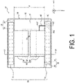
- FIG. 1 is a plan view of an antenna 10 according to an embodiment of the present disclosure.
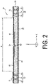
- FIG. 2 is a cross-sectional view of the antenna 10 taken along a line L1-L1 in FIG. 1 .
- the antenna 10 includes a base 20, a first conductor 30, a second conductor 33, a third conductor 40, a fourth conductor 50, a power supply line 60, and a reinforcing member 70.
- the first conductor 30 and the second conductor 33 are also referred to as a conductor pair.
- the antenna 10 may further include a connecting part 80.
- Each of the first conductor 30, the second conductor 33, the third conductor 40, the fourth conductor 50, and the power supply line 60 includes an electrically conductive material.
- the first conductor 30, the second conductor 33, the third conductor 40, the fourth conductor 50, and the power supply line 60 may include the same electrically conductive material or may include different electrically conductive materials.
- the antenna 10 may exhibit an artificial magnetic conductor character with respect to a predetermined frequency of electromagnetic waves externally incident on a plane where the third conductor 40 is located.
- the "artificial magnetic conductor character” means a characteristic of a plane where a phase difference between an incident wave and a reflected wave at one resonant frequency is 0 degrees.
- the antenna 10 can have an operating frequency in the vicinity of at least one resonant frequency.
- the phase difference between the incident wave and the reflected wave at the operating frequency band is smaller than a range from -90 degrees to +90 degrees.
- At least a portion of the antenna 10 may be flexible.
- a region A of the antenna 10 may be bent in the X direction depending on the placement location and the like of the antenna 10.
- the region A is a partial region of the antenna 10 in the X direction.
- the region A may be a region including the third conductor 40.
- the region A may be a region not including the first conductor 30 or the second conductor 33.
- the region A of the antenna 10 may be bent toward the Z-axis positive direction with respect to the X direction as illustrated in FIG. 3 described later, or may be bent toward the Z-axis negative direction as illustrated in FIG. 4 described later.
- the antenna 10 may be configured as a flexible printed circuit (FPC).
- the base 20 includes a dielectric material.
- the base 20 may have any shape depending on a shape of the third conductor 40 and the like.
- the base 20 may have a substantially rectangular parallelepiped shape.
- a relative permittivity of the base 20 may be adjusted as appropriate depending on the desired operating frequency of the antenna 10.
- the base 20 includes an upper surface 21 and a lower surface 22.
- the upper surface 21 is a surface on the Z-axis positive direction side, of two planes substantially parallel with the XY plane included in the base 20.
- the lower surface 22 is a surface on the Z-axis negative direction side, of two planes substantially parallel with the XY plane included in the base 20.
- the first conductor 30 is positioned closer to the X-axis negative direction side than the second conductor 33.
- the first conductor 30 may be positioned at an end portion of the base 20 on the X-axis negative direction side.
- the first conductor 30 extends along the Y direction.
- the first conductor 30 includes at least one first connection conductor 31 and a first electrical conductor layer 32.
- the first connection conductor 31 and the first electrical conductor layer 32 may include the same electrically conductive material, or may include different electrically conductive materials.
- a plurality of first connection conductors 31 may be aligned at intervals in the Y direction.
- the plurality of first connection conductors 31 may be spaced apart at substantially equal intervals and aligned in the Y direction.
- the plurality of first connection conductors 31 may be aligned in two rows in the Y direction. However, the first connection conductor 31 may be aligned in one row in the Y direction, or may be aligned in three or more rows in the Y direction.
- the first connection conductor 31 extends along the Z direction from the fourth conductor 50 to the first electrical conductor layer 32.
- the first connection conductor 31 includes two end portions.
- the first connection conductor 31 may be configured to have one end portion electrically connected to the fourth conductor 50, and the other end portion electrically connected to the first electrical conductor layer 32.
- the first connection conductor 31 may be a through hole conductor, a via conductor, or the like.
- the first electrical conductor layer 32 is located on the upper surface 21 of the base 20.
- the first electrical conductor layer 32 may be planar.
- the first electrical conductor layer 32 may be substantially rectangular.
- the first electrical conductor layer 32 includes two surfaces substantially parallel with the XY plane. One of those two surfaces faces the fourth conductor 50.
- the first electrical conductor layer 32 is configured to be electrically connected to the third conductor 40.
- the first electrical conductor layer 32 may be configured such that the surface facing the fourth conductor 50 of two surfaces substantially parallel with the XY plane of the first electrical conductor layer 32 is electrically connected to the end portion of the first connection conductor 31.
- the first electrical conductor layer 32 may be configured such that a portion of an end portion of the first electrical conductor layer 32 on the X-axis positive direction side is electrically connected to a fifth conductor 41 (described later) of the third conductor 40.
- the second conductor 33 faces the first conductor 30 in the X direction.
- the second conductor 33 is positioned closer to the X-axis positive direction side than the first conductor 30.
- the second conductor 33 may be positioned at an end portion of the base 20 on the X-axis positive direction side.
- the second conductor 33 extends along the Y direction.
- the second conductor 33 includes at least one second connection conductor 34 and a second electrical conductor layer 35.
- the second connection conductor 34 and the second electrical conductor layer 35 may include the same electrically conductive material, or may include different electrically conductive materials.
- a plurality of second connection conductors 34 may be aligned at intervals in the Y direction.
- the plurality of second connection conductors 34 may be spaced apart at substantially equal intervals and aligned in the Y direction.
- the plurality of second connection conductors 34 may be aligned in two rows in the Y direction. However, the second connection conductor 34 may be aligned in one row in the Y direction, or may be aligned in three or more rows in the Y direction.
- the second connection conductor 34 extends along the Z direction from the fourth conductor 50 to the second electrical conductor layer 35.
- the second connection conductor 34 includes two end portions.
- the second connection conductor 34 may be configured to have one end portion electrically connected to the fourth conductor 50, and the other end portion electrically connected to the second electrical conductor layer 35.
- the second connection conductor 34 may be a through hole conductor, a via conductor, or the like.
- the second electrical conductor layer 35 is located on the upper surface 21 of the base 20.
- the second electrical conductor layer 35 may be planar.
- the second electrical conductor layer 35 may be substantially rectangular.
- the second electrical conductor layer 35 includes two surfaces substantially parallel with the XY plane. One of those two surfaces faces the fourth conductor 50.
- the second electrical conductor layer 35 may include an opening portion 35a. A portion of the connecting part 80 is located in the opening portion 35a.
- the second electrical conductor layer 35 is configured to be electrically connected to the third conductor 40.
- the second electrical conductor layer 35 may be configured such that the surface facing the fourth conductor of two surfaces substantially parallel with the XY plane of the second electrical conductor layer 35 is electrically connected to the end portion of the second connection conductor 34.
- the second electrical conductor layer 35 may be configured such that a portion of an end portion of the second electrical conductor layer 35 on the X-axis negative direction side is electrically connected to a sixth conductor 42 (described later) of the third conductor 40.
- the third conductor 40 extends along the X direction.
- the third conductor 40 may extend along the XY plane.
- the third conductor 40 is located between the first conductor 30 and the second conductor 33.
- the third conductor 40 includes the fifth conductor 41, the sixth conductor 42, and an inner conductor 43.
- the fifth connection conductor 41, the sixth conductor 42, and the inner conductor 43 may include the same electrically conductive material, or may include different electrically conductive materials.
- the fifth conductor 41 and the sixth conductor 42 are located on the upper surface 21 of the base 20. A portion of the fifth conductor 41 and a portion of the sixth conductor 42 may be located inside the base 20. The fifth conductor 41 and the sixth conductor 42 may be substantially rectangular.
- the fifth conductor 41 is configured to be electrically connected to the first electrical conductor layer 32 of the first conductor 30.
- the fifth conductor 41 may be configured to have an end portion on the X-axis negative direction side that is electrically connected to the first electrical conductor layer 32.
- the end portion of the fifth conductor 41 on the X-axis negative direction side may be integrated with a portion of the end portion of the first electrical conductor layer 32.
- the sixth conductor 42 is configured to be electrically connected to the second electrical conductor layer 35 of the second conductor 33.
- the sixth conductor 42 may be configured to have an end portion on the X-axis positive direction side that is electrically connected to the second electrical conductor layer 35.
- the end portion of the sixth conductor 42 on the X-axis positive direction side may be integrated with a portion of the end portion of the first electrical conductor layer 32.
- the end portion of the fifth conductor 41 on the X-axis positive direction side faces the end portion of the sixth conductor 42 on the X-axis negative direction side.
- a gap S1 is located between the end portion of the fifth conductor 41 on the X-axis positive direction side and the end portion of the sixth conductor 42 on the X-axis negative direction side.
- the fifth conductor 41 and the sixth conductor 42 may be capacitively connected to each other because the gap S1 is located between the end portion of the fifth conductor 41 on the X-axis positive direction side and the end portion of the sixth conductor 42 on the X-axis negative direction side.
- the width of the gap S1 in the X direction may be adjusted as appropriate depending on the desired operating frequency of the antenna 10.
- the inner conductor 43 is located inside the base 20.
- the inner conductor 43 is not electrically connected to the fifth conductor 41 or the sixth conductor 42.
- the inner conductor 43 is positioned closer to the Z-axis negative direction side than the fifth conductor 41 and the sixth conductor 42.
- the inner conductor 43 may be substantially rectangular.
- the inner conductor 43 is configured to capacitively connect the fifth conductor 41 to the sixth conductor 42.
- the inner conductor 43 is separated from the fifth conductor 41 and the sixth conductor 42.
- a portion of the inner conductor 43 may overlap a portion of the fifth conductor 41.
- another portion of the inner conductor 43 may overlap a portion of the sixth conductor 42.
- the inner conductor 43 may be capacitively connected to the fifth conductor 41 and the sixth conductor 42 because the inner conductor 43 overlaps a portion of the fifth conductor 41 and a portion of the sixth conductor 42 in the XY plane.
- the third conductor 40 is configured to capacitively connect the first conductor 30 to the second conductor 33.
- the fifth conductor 41 is configured to be electrically connected to the first electrical conductor layer 32 of the first conductor 30.
- the sixth conductor 42 is configured to be electrically connected to the second electrical conductor layer 35 of the second conductor 33.
- the fifth conductor 41 and the sixth conductor 42 may be capacitively connected to each other by the gap S1 and the inner conductor 43.
- the fourth conductor 50 extends along the X direction.
- the fourth conductor 50 may extend along the XY plane.
- the fourth conductor 50 is separate from the third conductor 40.
- the fourth conductor 50 may face the third conductor 40.
- the fourth conductor 50 may be located on the lower surface 22 of the base 20. A portion of the fourth conductor 50 may be located inside the base 20.
- the fourth conductor 50 may have any shape depending on the shape of the third conductor 40.
- the fourth conductor 50 may be substantially rectangular.
- the fourth conductor 50 is configured to be electrically connected to the first conductor 30 and the second conductor 33.
- the fourth conductor 50 is configured to have a portion on the X-axis negative direction side that is electrically connected to the end portion of the first electrical conductor layer 31 of the first conductor 30.
- the fourth conductor 50 is configured to have a portion on the X-axis positive direction side that is electrically connected to the second electrical conductor layer 34 of the second conductor 33.
- the fourth conductor 50 is configured to supply a potential that is a reference for the antenna 10.
- the fourth conductor 50 may be configured to be electrically connected to the ground of a device provided with the antenna 10.
- the fourth conductor 50 may be configured to have a portion electrically connected to a ground conductor 91 of a circuit substrate 90.
- a variety of parts of the device provided with the antenna 10 may be located on the Z-axis negative direction side of the fourth conductor 50.
- the antenna 10 can maintain a radiation efficiency at the operating frequency because of having the artificial magnetic conductor character described above, even if the variety of parts are located on the Z-axis negative direction side of the fourth conductor 50.
- the power supply line 60 is configured to be electromagnetically connected to the third conductor 40.
- the "electromagnetic connection” may be an electrical connection or a magnetic connection.
- the power supply line 60 is configured to have one end electrically connected to the sixth conductor 42 of the third conductor 40.
- the power supply line 60 is configured to have the other end electrically connected to the connecting part 80.
- the power supply line 60 may be located on the upper surface 21 of the base 20. A portion of the power supply line 60 may be located inside the base 20.
- the power supply line 60 is configured to supply electrical power from an RF module or the like via the connecting part 80 to the third conductor 40 when the antenna 10 emits electromagnetic waves.
- the power supply line 60 is configured to supply electrical power from the third conductor 40 via the connecting part 80 to the RF module or the like when the antenna 10 receives electromagnetic waves.
- a loop current may be generated that flows in a loop through the first conductor 30, the second conductor 33, the third conductor 40, and the fourth conductor 50.
- the first conductor 30 is seen as an electrical wall extending along the YZ plane on the X-axis negative direction side
- the second conductor 33 is seen as an electrical wall extending along the YZ plane on the X-axis positive direction side.
- the conductor or the like is not located on the Y-axis positive and negative direction sides. In other words, from the perspective of the loop current, the Y-axis positive and negative direction sides are electrically open.
- the XZ plane on the Y-axis positive direction side and the XY plane on the Y-axis negative direction side are seen as magnetic walls from the perspective of the loop current.
- the loop current is surrounded by these two electrical walls and two magnetic walls, thus the antenna 10 exhibits the artificial magnetic conductor character with respect to a predetermined frequency of electromagnetic waves incident on the upper surface 21 of the base 20 from the Z-axis positive direction side.
- the reinforcing member 70 is configured to protect at least a portion of any of the first conductor 30 and the second conductor 33.
- the reinforcing member 70 is located on at least a portion of any of the first conductor 30 and the second conductor 33.
- the reinforcing member 70 includes a first reinforcing member 71 and a second reinforcing member 72.
- the reinforcing member 70 may include at least one of the first reinforcing member 71 and the second reinforcing member 72 depending on the placement location and the like of the antenna 10.
- Each of the first reinforcing member 71 and the second reinforcing member 72 includes a dielectric material.
- the first reinforcing member 71 and the second reinforcing member 72 may include the same dielectric material, or may include different dielectric materials.
- the first reinforcing member 71 may be located on at least a portion of the first conductor 30.
- the first reinforcing member 71 may be located on the first electrical conductor layer 32.
- the first reinforcing member 71 may be located on the first electrical conductor layer 32 so as to be positioned at the end portion of the first connection conductor 31.
- the first reinforcing member 71 may extend on the first electrical conductor layer 32 so as to be positioned at the end portions of the plurality of first connection conductors 31.
- the area of the first reinforcing member 71 in the XY plane may be smaller than the area of the first electrical conductor layer 32 in the XY plane.
- the area of the first reinforcing member 71 in the XY plane may be an area capable of covering the end portions of the plurality of first connection conductors 31.
- the shape of the first reinforcing member 71 may depend on the arrangement of the first connection conductors 31 in the XY plane. For example, when the plurality of first connection conductors 31 are aligned in two rows in the Y direction, the shape of the first reinforcing member 71 may be substantially rectangular.
- the material of the first reinforcing member 71 and the thickness of the first reinforcing member 71 in the Z direction may be selected as appropriate in consideration of a stress applied to the first conductor 30.
- the region A of the antenna 10 may bend toward the Z-axis positive direction with respect to the X direction.
- the first reinforcing member 71 being located on at least a portion of the first conductor 30 may reduce the degree of deformation of the first conductor 30 when the region A of the antenna 10 is bent.
- the degree of deformation of the first conductor 30 being reduced may reduce the stress applied to the first connection conductor 31.
- the stress applied to the first connection conductor 31 being reduced may reduce the likelihood of the first connection conductor 31 breaking.
- the first reinforcing member 71 being located on the first electrical conductor layer 32 so as to be positioned at the end portion of the first connection conductor 31 may further reduce the stress applied to the first connection conductor 31.
- the stress applied to the first connection conductor 31 being further reduced may further reduce the likelihood of the first connection conductor 31 breaking.
- the second reinforcing member 72 may be located on at least a portion of the second conductor 33.
- the second reinforcing member 72 may be located on the second electrical conductor layer 35.
- the second reinforcing member 72 may be located on the second electrical conductor layer 35 so as to be positioned at the end portion of the second connection conductor 34.
- the second reinforcing member 72 may extend on the second electrical conductor layer 35 so as to be positioned at the end portions of the plurality of second connection conductors 34.
- the area of the second reinforcing member 72 in the XY plane may be smaller than the area of the second electrical conductor layer 35 in the XY plane.
- the area of the second reinforcing member 72 in the XY plane may be an area capable of covering the end portions of the plurality of second connection conductors 34.
- the shape of the second reinforcing member 72 may depend on the arrangement of the second connection conductors 34 in the XY plane. For example, when the plurality of second connection conductors 34 are aligned in two rows in the Y direction, the shape of the second reinforcing member 72 may be substantially rectangular.
- the material of the second reinforcing member 72 and the thickness of the second reinforcing member 72 in the Z direction may be selected as appropriate in consideration of a stress applied to the second conductor 33.
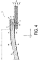
- the region A of the antenna 10 may bend toward the Z-axis negative direction with respect to the X direction.
- the configuration illustrated in FIG. 4 corresponds to a cross-sectional view taken along a line L2-L2 in FIG. 1 .
- the second reinforcing member 72 being located on at least a portion of the second conductor 33 may reduce the likelihood of the second connection conductor 34 breaking, similar to the first reinforcing member 71.
- the second reinforcing member 72 being located on the second electrical conductor layer 35 so as to be positioned at the end portion of the second connection conductor 34 may further reduce the likelihood of breaking the second connection conductor 34, similar to the first reinforcing member 71.
- the second reinforcing member 72 may be located to overlap the connecting part 80 in the XY plane.
- the second reinforcing member 72 may be located on the second electrical conductor layer 35 to cover the opening portion 35a.
- the second reinforcing member 72 being located to overlap the connecting part 80 in the XY plane may reduce the degree of deformation of the connecting part 80 and a solder 95 described later.
- the degree of deformation of the connecting part 80 and the solder 95 described later being reduced may reduce a stress applied to the connecting part 80 and the solder 95 described later.
- the stress applied to the connecting part 80 and the solder 95 described later being reduced may reduce the likelihood of the connecting part 80 and the solder 95 (described later) breaking.
- the connecting part 80 is aligned with the second connection conductor 34 in the Y direction.
- the connecting part 80 may be located closer to the Y-axis positive direction side than the second connection conductor 34.
- the connecting part 80 is configured to electrically connect the power supply line 60 to the circuit substrate 90.
- the connecting part 80 may be any part.
- the connecting part 80 may be a connector of a surface mount technology (SMT) type.
- the circuit substrate 90 may be one of parts of the device provided with the antenna 10.
- the circuit substrate 90 may be a multilayer substrate.
- the circuit substrate 90 is located on the Z-axis negative direction side of the antenna 10. In the configuration illustrated in FIG. 4 , a portion of the antenna 10 may overlap a portion of the circuit substrate 90 in the XY plane. However, as illustrated in FIG. 12 described later, the antenna 10 may entirely overlap the circuit substrate 90 in the XY plane.
- the circuit substrate 90 in the case of overlapping a portion of the antenna 10, may be configured as a printed circuit board (PCB), for example.
- the circuit substrate 90, in the case of entirely overlapping the antenna 10, may be configured as a flexible printed circuit, for example.
- the circuit substrate 90 includes a ground conductor 91, an insulating layer 92, an insulating layer 93, a wiring layer 94, and the solder 95.
- the ground conductor 91 includes an electrically conductive material.
- the ground conductor 91 is located on the Z-axis positive direction side of the circuit substrate 90.
- the ground conductor 91 is configured to be electrically connected to the ground of the device provided with the antenna 10.
- Each of the insulating layer 92 and the insulating layer 93 includes any insulating material.
- the insulating layer 92 is located on the Z-axis negative direction side of the ground conductor 91.
- the insulating layer 93 is located on the Z-axis negative direction side of the wiring layer 94.
- the wiring layer 94 is located between the insulating layer 92 and the insulating layer 93.
- the wiring layer 94 includes a wiring pattern 94A and an insulating layer 94B including any insulating material.
- the wiring pattern 94A includes an electrically conductive material.
- the wiring pattern 94A is configured to be electrically connected to the RF module.
- the solder 95 is located in a portion of the wiring pattern 94A.
- the wiring pattern 94A may be electrically connected to the connecting part 80 by the solder 95.
- the solder 95 is located between the connecting part 80 and the wiring pattern 94A.
- the solder 95 is configured to electrically connect the connecting part 80 to the wiring pattern 94A.
- the antenna 10 includes the reinforcing member 70 located on at least a portion of any of the first conductor 30 and the second conductor 33.
- the first reinforcing member 71 may reduce the degree of deformation of the first conductor 30 when the region A of the antenna 10 is bent. The degree of deformation of the first conductor 30 being reduced may reduce the likelihood of the first connection conductor 31 breaking.
- the second reinforcing member 72 may reduce the degree of deformation of the second conductor 33 when the region A of the antenna 10 is bent. The degree of deformation of the second conductor 33 being reduced may reduce the likelihood of the second connection conductor 34 breaking.
- the novel antenna 10 excellent in long-term reliability can be provided.
- FIG. 5 is a plan view of an antenna 110 according to another embodiment of the present disclosure.
- FIG. 6 is a diagram illustrating an example of a usage state of the antenna 110 illustrated in FIG. 5 .
- the configuration illustrated in FIG. 6 corresponds to the cross-sectional view taken along a line L3-L3 in FIG. 5 .
- the antenna 110 includes the base 20, the first conductor 30, the second conductor 33, the third conductor 40, the fourth conductor 50, the power supply line 60, and a reinforcing member 170.
- the antenna 110 may further include a connecting part 180.
- the antenna 110 may exhibit the artificial magnetic conductor character with respect to a predetermined frequency of electromagnetic waves externally incident on a plane where the third conductor 40 is located, in the same manner as or similar manner to the antenna 10. At least a portion of the antenna 110 may be flexible in the same manner as or similar manner to the antenna 10.
- the antenna 110 may be configured as a flexible printed circuit.
- a circuit substrate 190 is located at a portion of the antenna 110.
- the circuit substrate 190 is located on the Z-axis positive direction side of the antenna 110.
- the reinforcing member 170 is configured to protect at least a portion of any of the first conductor 30 and the second conductor 33.
- the reinforcing member 170 is located on at least a portion of any of the first conductor 30 and the second conductor 33.
- the reinforcing member 170 includes the first reinforcing member 71 and a second reinforcing member 172.
- the reinforcing member 170 may include at least one of the first reinforcing member 71 and the second reinforcing member 172 depending on the placement location and the like of the antenna 10.
- the second reinforcing member 172 includes a dielectric material.
- the second reinforcing member 172 may be located on at least a portion of the second conductor 33.
- the second reinforcing member 172 may be located on the second electrical conductor layer 35.
- the second reinforcing member 172 need not be located on a portion in the second electrical conductor layer 35 where the connecting part 80 and the circuit substrate 190 are located.
- Other configurations of the second reinforcing member 172 are the same as or similar to the second reinforcing member 72 as illustrated in FIG. 1 .
- the region A of the antenna 110 may bend toward the Z-axis negative direction.
- the second reinforcing member 172 being located on at least a portion of the second conductor 33 may reduce the likelihood of the second connection conductor 34 breaking, similar to the second reinforcing member 72.
- the second reinforcing member 172 being located above the end portion of the second connection conductor 34 may further reduce the likelihood of the second connection conductor 34 breaking, similar to the second reinforcing member 72.
- the connecting part 180 is aligned with the second connection conductor 34 in the Y direction.
- the connecting part 180 may be located closer to the Y-axis positive direction side than the second connection conductor 34.
- the connecting part 180 is configured to electrically connect the power supply line 60 to the circuit substrate 190.
- the connecting part 180 may be any part.
- the connecting part 180 may be a connector of a surface mount technology type.
- the circuit substrate 190 may be one of parts of the device provided with the antenna 110.
- the circuit substrate 190 may be a multilayer substrate.
- the circuit substrate 190 is located on the Z-axis positive direction side of the antenna 110.
- a portion of the circuit substrate 190 may overlap a portion of the antenna 110 on the X-axis positive direction side in the XY plane.
- the circuit substrate 190 includes an insulating layer 191, an insulating layer 192, a wiring layer 193, and a solder 194.
- Each of the insulating layer 191 and the insulating layer 192 includes any insulating material.
- the insulating layer 191 is a lowermost layer.
- the insulating layer 191 is located on the antenna 110.
- the insulating layer 192 is located on the Z-axis positive direction side of the wiring layer 193.
- the wiring layer 193 is located between the insulating layer 191 and the insulating layer 192.
- the wiring layer 193 includes a wiring pattern 193A and an insulating layer 193B including any insulating material.
- the wiring pattern 193A includes an electrically conductive material.
- the wiring pattern 193A is configured to be electrically connected to the RF module.
- the solder 194 is located in a portion of the wiring pattern 193A.
- the wiring pattern 193A may be electrically connected to the connecting part 180 by the solder 194.
- the solder 194 is located between the connecting part 180 and the wiring pattern 193A.
- the solder 194 is configured to electrically connect the connecting part 180 to the wiring pattern 193A.
- antenna 110 Other configurations and effects of the antenna 110 are the same or similar to those of the antenna 10 as illustrated in FIG. 1 .
- FIG. 7 is a plan view of an antenna 210 according to still another embodiment of the present disclosure.
- the antenna 210 includes the base 20, a first conductor 230, a second conductor 233, the third conductor 40, the fourth conductor 50, the power supply line 60, and a reinforcing member 270.
- the antenna 210 may further include the connecting part 80.
- Each of the first conductor 230 and the second conductor 233 includes an electrically conductive material.
- the first conductor 230, the second conductor 233, the third conductor 40, the fourth conductor 50, and the power supply line 60 may include the same electrically conductive material or may include different electrically conductive materials.
- the antenna 210 may exhibit the artificial magnetic conductor character with respect to a predetermined frequency of electromagnetic waves externally incident on a plane where the third conductor 40 is located, in the same manner as or similar manner to the antenna 10.
- At least a portion of the antenna 210 may be flexible.
- the region A of the antenna 210 may be bent in the X direction depending on the placement location and the like of the antenna 210.
- a region B of the antenna 210 may be bent in the Y direction.
- the region B of the antenna 210 may be bent toward the Z-axis positive direction with respect to the Y direction, or may be bent toward the Z-axis negative direction.
- the region B is a partial region of the antenna 210 in the Y direction. Part or all of the region B may overlap part or all of the region A.
- the region B may be a region including at least a portion of the third conductor 40.
- the region B may be a region not including the first connection conductor 31 or the second connection conductor 34.
- the antenna 210 may be configured as a flexible printed circuit.
- the circuit substrate 90 is located at a portion of the antenna 210 similar to the configuration illustrated in FIG. 4 .
- the circuit substrate 90 is located on the Z-axis negative direction side of the antenna 210 similar to the configuration illustrated in FIG. 4 .
- the first conductor 230 includes a first connection conductor set 231A, a first connection conductor set 231B, and the first electrical conductor layer 32.
- first connection conductor set 231A and the first connection conductor set 231B are not particularly distinguished, they are collectively referred to as the "first connection conductor set 231".
- the first connection conductor set 231 includes at least one first connection conductor 31.
- the plurality of first connection conductors 31 may be aligned in two rows in the Y direction.
- the first connection conductor set 231A and the first connection conductor set 231B are separated from each other by a first interval in the Y direction.
- the first interval is wider than an interval at which the first connection conductors 31 are aligned in the Y direction in the first connection conductor set 231.
- the first interval may be set as appropriate in consideration of a curvature of the region B of the antenna 210 in the Y direction.
- the first connection conductor set 231A is located near a corner portion, of four corner portions of the fifth conductor 41, on the X-axis negative direction side and the Y-axis negative direction side.
- the first connection conductor set 231B is located near a corner portion, of four corner portions of the fifth conductor 41, on the X-axis negative direction side and the Y-axis positive direction side.
- first conductor 230 Other configurations of the first conductor 230 are the same as or similar to those of the first conductor 30 as illustrated in FIG. 1 .
- the second conductor 233 includes a second connection conductor set 234A, a second connection conductor set 234B, and the second electrical conductor layer 35.
- second connection conductor set 234A and the second connection conductor set 234B are not particularly distinguished, they are collectively referred to as the "second connection conductor set 234".
- the second connection conductor set 234 includes at least one second connection conductor 34.
- the plurality of second connection conductors 34 may be aligned in two rows in the Y direction.
- the second connection conductor set 234A and the second connection conductor set 234B are separated from each other by a second interval in the Y direction.
- the second interval may be the same as the first interval, or may be different from the first interval.
- the second interval is wider than an interval at which the second connection conductors 34 are aligned in the Y direction in the second connection conductor set 234.
- the second interval may be set as appropriate in consideration of the curvature of the region B of the antenna 210 in the Y direction.
- the second connection conductor set 234A is located near a corner portion, of four corner portions of the sixth conductor 42, on the X-axis positive direction side and the Y-axis negative direction side.
- the second connection conductor set 234B is located near a corner portion, of four corner portions of the sixth conductor 42, on the X-axis positive direction side and the Y-axis positive direction side.
- the reinforcing member 270 is configured to protect at least a portion of any of the first conductor 230 and the second conductor 233.
- the reinforcing member 270 is located on at least a portion of any of the first conductor 230 and the second conductor 233.
- the reinforcing member 270 includes a first reinforcing member 271 and a second reinforcing member 272, the first reinforcing member 271 including a third reinforcing member 273A and a third reinforcing member 273B, the second reinforcing member 272 including a fourth reinforcing member 274A and a fourth reinforcing member 274B.
- the reinforcing member 270 may include at least one of the third reinforcing member 273A, the third reinforcing member 273B, the fourth reinforcing member 274A, and the fourth reinforcing member 274B depending on the placement location and the like of the antenna 210.
- the third reinforcing member 273A and the third reinforcing member 273B are not particularly distinguished, they are referred to as the "third reinforcing member 273".
- the fourth reinforcing member 274A and the fourth reinforcing member 274B are not particularly distinguished, they are referred to as the "fourth reinforcing member 274".
- Each of the third reinforcing member 273 and the fourth reinforcing member 274 includes a dielectric material.
- the third reinforcing member 273A, the third reinforcing member 273B, the fourth reinforcing member 274A, and the fourth reinforcing member 274B may include the same dielectric material, or may include different dielectric materials.
- Each of the third reinforcing member 273A and the third reinforcing member 273B is located on the first electrical conductor layer 32.
- the third reinforcing member 273A and the third reinforcing member 273B are separated from each other in the Y direction.
- the third reinforcing member 273A is located in the first connection conductor set 231A.
- the third reinforcing member 273A may be located on the first electrical conductor layer 32 so as to be positioned at the end portion of the first connection conductor 31 in the first connection conductor set 231A.
- the third reinforcing member 273A may extend on the first electrical conductor layer 32 so as to be positioned at the end portions of the plurality of first connection conductors 31 in the first connection conductor set 231A.
- the third reinforcing member 273B is located in the first connection conductor set 231B.
- the third reinforcing member 273B may be located on the first electrical conductor layer 32 so as to be positioned at the end portion of the first connection conductor 31 in the first connection conductor set 231B.
- the third reinforcing member 273B may extend on the first electrical conductor layer 32 so as to be positioned at the end portions of the plurality of first connection conductors 31 in the first connection conductor set 231B.
- the area of the third reinforcing member 273 in the XY plane may be an area capable of covering the end portions of the first connection conductors 31 included in the first connection conductor set 231.
- the shape of the third reinforcing member 273 may depend on the arrangement of the first connection conductors 31 in the first connection conductor set 231 in the XY plane. For example, when the plurality of first connection conductors 31 are aligned in two rows in the Y direction in the first connection conductor set 231, the shape of the third reinforcing member 273 may be substantially rectangular.
- the material and the thickness in the Z direction of the third reinforcing member 273 may be selected as appropriate in consideration of a stress applied to the first conductor 230.
- the region A of the antenna 210 may bend toward the Z-axis positive direction similar to the configuration illustrated in FIG. 3 .
- the third reinforcing member 273 being located in the first connection conductor set 231 may reduce the stress applied to the first connection conductor 31 and reduce the likelihood of the first connection conductor 31 breaking.
- the region B of the antenna 210 may be bent in the Y direction. When the region B of the antenna 210 is bent, the third reinforcing member 273 being located in the first connection conductor set 231 may reduce the stress applied to the first connection conductor 31 and reduce the likelihood of the first connection conductor 31 breaking.
- Each of the fourth reinforcing member 274A and the fourth reinforcing member 274B is located on the second electrical conductor layer 35.
- the fourth reinforcing member 274A and the fourth reinforcing member 274B are separated from each other in the Y direction.
- the fourth reinforcing member 274A is located in the second connection conductor set 234A.
- the fourth reinforcing member 274A may be located on the second electrical conductor layer 35 so as to be positioned at the end portion of the second connection conductor 34 in the second connection conductor set 234A.
- the fourth reinforcing member 274A may extend on the second electrical conductor layer 35 so as to be positioned at the end portions of the plurality of second connection conductors 34 in the second connection conductor set 234A.
- the fourth reinforcing member 274B is located in the second connection conductor set 234B.
- the fourth reinforcing member 274B may be located on the second electrical conductor layer 35 so as to be positioned at the end portion of the second connection conductor 34 in the second connection conductor set 234B.
- the fourth reinforcing member 274B may extend on the second electrical conductor layer 35 so as to be positioned at the end portions of the plurality of second connection conductors 34 in the second connection conductor set 234B.
- the area of the fourth reinforcing member 274 in the XY plane may be an area capable of covering the end portions of the plurality of second connection conductors 34 included in the second connection conductor set 234.
- the shape of the fourth reinforcing member 274 may depend on the arrangement of the second connection conductors 34 in the second connection conductor set 234 in the XY plane. For example, when the plurality of second connection conductors 34 are aligned in two rows in the Y direction in the second connection conductor set 234, the shape of the fourth reinforcing member 274 may be substantially rectangular.
- the material and the thickness in the Z direction of the fourth reinforcing member 274 may be selected as appropriate in consideration of a stress applied to the second conductor 233.
- the fourth reinforcing member 274 being located in the second connection conductor set 234 may reduce the likelihood of the second connection conductor 34 breaking in the second connection conductor set 234, in the same manner as or similar manner to the third reinforcing member 273.
- the fourth reinforcing member 274 being located in the second connection conductor set 234 may reduce the stress applied to the second connection conductor 34 and reduce the likelihood of the second connection conductor 34 breaking.
- the fourth reinforcing member 274B may be located to overlap the connecting part 80 in the XY plane. Similar to the configuration illustrated in FIG. 4 , the fourth reinforcing member 274B being located to overlap the connecting part 80 may reduce the degree of deformation of the connecting part 80 and the solder 95 and reduce the likelihood of the connecting part 80 and the solder 95 breaking.
- antenna 210 Other configurations and effects of the antenna 210 are the same or similar to those of the antenna 10 as illustrated in FIG. 1 .
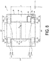
- FIG. 8 is a plan view of an antenna 310 according to still another embodiment of the present disclosure.
- the antenna 310 includes the base 20, the first conductor 230, the second conductor 233, the third conductor 40, the fourth conductor 50, the power supply line 60, and a reinforcing member 370.
- the antenna 310 may further include the connecting part 180.
- the antenna 310 may exhibit the artificial magnetic conductor character with respect to a predetermined frequency of electromagnetic waves externally incident on a plane where the third conductor 40 is located, in the same manner as or similar manner to the antenna 10. At least a portion of the antenna 310 may be flexible similar to the antenna 210.
- the antenna 310 may be configured as a flexible printed circuit.
- the circuit substrate 190 is located at a portion of the antenna 310 similar to the configuration illustrated in FIGS. 5 and 6 .
- the circuit substrate 190 is located on the Z-axis positive direction side of the antenna 210 similar to the configuration illustrated in FIG. 6 .
- the reinforcing member 370 includes the first reinforcing member 271 and a second reinforcing member 372.
- the second reinforcing member 372 includes the fourth reinforcing member 274A and a fourth reinforcing member 374B.
- the fourth reinforcing member 374B includes a dielectric material.
- the fourth reinforcing member 374B, the third reinforcing member 273A, the third reinforcing member 273B, and the fourth reinforcing member 274A may include the same dielectric material, or may include different dielectric materials.
- the fourth reinforcing member 374B need not be located on a portion in the second electrical conductor layer 35 where the connecting part 180 and the circuit substrate 190 are located.
- Other configurations of the fourth reinforcing member 374B are the same as or similar to those of the fourth reinforcing member 274.
- antenna 310 Other configurations and effects of the antenna 310 are the same or similar to those of the antenna 10 as illustrated in FIG. 1 , the antenna 110 as illustrated in FIG. 5 , and/or the antenna 210 as illustrated in FIG. 7 .
- FIG. 9 is a plan view of an antenna 410 according to still another embodiment of the present disclosure.
- the antenna 410 includes the base 20, a first conductor 430, a second conductor 433, a third conductor 440, the fourth conductor 50, the power supply line 60, and the reinforcing member 270.
- the antenna 410 may further include the connecting part 80.
- the antenna 410 may include the connecting part 180 instead of the connecting part 80.
- the antenna 410 may include the reinforcing member 370 instead of the reinforcing member 270.
- Each of the first conductor 430, the second conductor 433, and the third conductor 440 includes an electrically conductive material.
- the first conductor 430, the second conductor 433, the third conductor 440, the fourth conductor 50, and the power supply line 60 may include the same electrically conductive material or may include different electrically conductive materials.
- the antenna 410 may exhibit the artificial magnetic conductor character with respect to a predetermined frequency of electromagnetic waves externally incident on a plane where the third conductor 440 is located.
- At least a portion of the antenna 410 may be flexible in the same manner as or similar manner to the antenna 210.
- the antenna 410 may be configured as a flexible printed circuit.
- the first conductor 430 includes the first connection conductor set 231A, the first connection conductor set 231B, and a first electrical conductor layer 432.
- the second conductor 433 includes the second connection conductor set 234A, the second connection conductor set 234B, and a second electrical conductor layer 435.
- the first electrical conductor layer 432 includes a cut portion 432a.
- the cut portion 432a is located near the center of the antenna 410 in the Y direction.
- the second electrical conductor layer 435 includes a cut portion 435a.
- the cut portion 435a is located near the center of the antenna 410 in the Y direction.
- the cut portions 432a and 435a extend along the X direction.
- Other configurations of the first and second electrical conductor layers 432 and 435 are the same or similar to those of the first and second electrical conductor layers 32 and 35, respectively.
- the third conductor 440 includes a fifth conductor 441, a sixth conductor 442, and the inner conductor 43.
- the fifth conductor 441 includes a cut portion 441a.
- the cut portion 441a is located near the center of the antenna 410 in the Y direction.
- the cut portion 441a may be connected to the cut portion 432a of the first electrical conductor layer 432.
- the sixth conductor 442 includes a cut portion 442a.
- the cut portion 442a is located near the center of the antenna 410 in the Y direction.
- the cut portion 442a may be connected to the cut portion 435a of the second electrical conductor layer 435.
- the cut portions 441a and 442a extend along the X direction.
- third conductor 440 Other configurations of the third conductor 440 are the same as or similar to those of the third conductor 40 as illustrated in FIG. 1 .
- the antenna 410 includes the cut portion 432a in the first electrical conductor layer 432, the cut portion 435a in the second electrical conductor layer 435, the cut portion 441a in the fifth electrical conductor layer 441, and the cut portion 442a in the sixth electrical conductor layer 442.
- the antenna 410 including the cut portion 432a, the cut portion 435a, the cut portion 441a, and the cut portion 442a enables the region B of the antenna 410 to be easily bent in the Y direction.
- the width of each of the cut portion 432a, the cut portion 435a, the cut portion 441a, and the cut portion 442a in the Y direction may be set as appropriate in consideration of the curvature of the region B of the antenna 410 in the Y direction.
- antenna 410 Other configurations and effects of the antenna 410 are the same as or similar to those of the antenna 10 as illustrated in FIG. 1 , the antenna 110 as illustrated in FIG. 5 , the antenna 210 as illustrated in FIG. 7 , and/or the antenna 310 as illustrated in FIG. 8 .
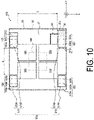
- FIG. 10 is a plan view of an antenna 510 according to still another embodiment of the present disclosure.
- the antenna 510 includes the base 20, conductor sets 530, 531, 532, and 533, radiation conductors 540, 541, 542, and 543, an inner conductor 544, the fourth conductor 50, the power supply line 60, and a reinforcing member 570.
- the antenna 510 may further include the connecting part 80.
- the antenna 510 may include the connecting part 180 instead of the connecting part 80.
- Each of the conductor sets 530 to 533, the radiation conductors 540 to 543, and the inner conductor 544 includes an electrically conductive material.
- the conductor sets 530 to 533, the radiation conductors 540 to 543, the inner conductor 544, the fourth conductor 50, and the power supply line 60 may include the same electrically conductive material or may include different electrically conductive materials.
- the antenna 510 may exhibit the artificial magnetic conductor character with respect to a predetermined frequency of electromagnetic waves externally incident on a plane where the radiation conductors 540 to 543 are located.
- At least a portion of the antenna 510 may be flexible.
- the antenna 510 may be configured as a flexible printed circuit.
- a region C of the antenna 510 may be bent in the X direction depending on the placement location and the like of the antenna 510.
- the region C is a partial region of the antenna 510 in the X direction.
- the region C may be a region including the radiation conductors 540 to 543.
- the region C may be a region not including the conductor sets 530 to 533.
- the antenna 510 may be bent toward the Z-axis positive direction with respect to the X direction similar to the configuration illustrated in FIG. 3 , or may be bent toward the Z-axis negative direction similar to the configuration illustrated in FIG. 4 .
- a region D of the antenna 510 may be bent in the Y direction depending on the placement location and the like of the antenna 510.
- the region D is a partial region of the antenna 510 in the Y direction.
- the region D may be a region including the radiation conductors 540 to 543.
- the region D may be a region not including the conductor sets 530 to 533.
- the region D of the antenna 510 may be bent toward the Z-axis positive direction with respect to the Y direction, or may be bent toward the Z-axis negative direction.
- the conductor set 530 and the conductor set 531 are aligned in the Y direction.
- the conductor set 532 and the conductor set 533 are aligned in the Y direction.
- the conductor set 530 and the conductor set 533 are aligned in the X direction.
- the conductor set 531 and the conductor set 532 are aligned in the X direction.
- the conductor sets 530, 531, 532, and 533 include connection portions 530a, 531a, 532a, and 533a, and at least one of connection conductors 530b, 531b, 532b, and 533b, respectively.
- the connection portions 530a to 533a and the connection conductors 530b to 533b may include the same electrically conductive material, or may include different electrically conductive materials.
- connection portions 530a to 533a are located on the upper surface 21 of the base 20.
- the connection portions 530a to 533a may be planar.
- the connection portions 530a to 533a may be substantially rectangular.
- a portion of the connection portion 530a is configured to be electrically connected to a corner portion, of four corner portions of the radiation conductor 540, on the Y-axis negative direction side and the X-axis negative direction side.
- a portion of the connection portion 531a is configured to be electrically connected to a corner portion, of four corner portions of the radiation conductor 541, on the Y-axis positive direction side and the X-axis negative direction side.
- connection portion 532a is configured to be electrically connected to a corner portion, of four corner portions of the radiation conductor 542, on the Y-axis positive direction side and the X-axis positive direction side.
- a portion of the connection portion 533a is configured to be electrically connected to a corner portion, of four corner portions of the radiation conductor 543, on the Y-axis negative direction side and the X-axis positive direction side.
- connection conductors 530b to 533b extend along the Z direction from the fourth conductor 50 toward the upper surface 21 of the base 20.
- Each of the connection conductors 530b to 533b includes two end portions.
- Each of the connection conductors 530b to 533b may be configured to have one end portion electrically connected to the fourth conductor 50.
- the connection conductors 530b to 533b may be configured to have the other end portions electrically connected to the respective connection portions 530a to 533a.
- Each of the connection conductors 530b to 533b may be a through hole conductor, a via conductor, or the like.
- the conductor sets 530 to 533 are configured to be electrically connected to the different respective radiation conductors 540 to 543.
- the conductor set 530 is configured to be electrically connected to the radiation conductor 540 by the connection portion 530a.
- the conductor set 531 is configured to be electrically connected to the radiation conductor 541 by the connection portion 531a.
- the conductor set 532 is configured to be electrically connected to the radiation conductor 542 by the connection portion 532a.
- the conductor set 533 is configured to be electrically connected to the radiation conductor 543 by the connection portion 533a.
- the radiation conductors 540 to 543 expand along the XY plane.
- the radiation conductors 540 to 543 are separate from each other in the X direction and the Y direction.
- the radiation conductors 540 to 543 may be planar.
- the radiation conductors 540 to 543 are separate from the fourth conductor 50 in the Z direction.
- the radiation conductors 540 to 543 may face the fourth conductor 50.
- the radiation conductors 540 to 543 may be located on the upper surface 21 of the base 20.
- the radiation conductor 540 and the radiation conductor 541 are spaced apart and aligned in the Y direction.
- the radiation conductor 542 and the radiation conductor 543 are spaced apart and aligned in the Y direction.
- the radiation conductor 540 and the radiation conductor 543 are spaced apart and aligned in the X direction.
- the radiation conductor 541 and the radiation conductor 542 are spaced apart and aligned in the X direction.
- the radiation conductors 540 to 533 are configured to be capacitively connected to each other by being spaced apart and aligned in the X and Y directions.
- the interval between the radiation conductor 540 and the radiation conductor 541 aligned in the Y direction, and the interval between the radiation conductor 542 and the radiation conductor 543 aligned in the Y direction may be adjusted as appropriate depending on the desired operating frequency of the antenna 510.
- the interval between the radiation conductor 540 and the radiation conductor 543 aligned in the X direction, and the interval between the radiation conductor 541 and the radiation conductor 542 aligned in the X direction may be adjusted as appropriate depending on the desired operating frequency of the antenna 510.
- the inner conductor 544 is located inside the base 20 similar to the inner conductor 43.
- the inner conductor 544 is not electrically connected to the radiation conductors 540 to 533.
- the inner conductor 544 is located closer to the Z-axis negative direction side than the radiation conductors 540 to 533.
- the inner conductor 544 may be substantially rectangular.
- the inner conductor 544 is configured to capacitively connect the radiation conductors 540 to 533 to each other.
- the inner conductor 544 is separate from the radiation conductors 540 to 533.
- a portion of the inner conductor 544 may overlap a portion of the radiation conductors 540 to 533 in the Z direction.
- a portion of the inner conductor 544 overlapping a portion of the radiation conductors 540 to 533 may be allowed to be capacitively connected to a portion of the radiation conductors 540 to 533.
- the power supply line 60 is configured to be electromagnetically connected to any of the radiation conductors 540 to 533.
- the power supply line 60 is configured to be electrically connected to the radiation conductor 542.
- connection conductor 530b and the connection conductor 533b are a first connection pair aligned along the X direction.
- the connection conductor 531b and the connection conductor 532b are a first connection pair aligned along the X direction.
- the antenna 510 may resonate at a first frequency along a first current path.
- the first current path includes the first connection pair of the connection conductors 530b and 533b, the radiation conductor 540, the radiation conductor 543, and the fourth conductor 50.
- the first current path includes the first connection pair of the connection conductors 531b and 532b, the radiation conductor 541, the radiation conductor 542, and the fourth conductor 50.
- connection conductors 530b and 531b are seen as an electrical wall extending along the YZ plane on the X-axis negative direction side
- connection conductors 532b and 533b are seen as an electrical wall extending along the YZ plane on the X-axis positive direction side
- the XZ plane on the Y-axis positive direction side is seen as a magnetic wall
- the XZ plane on the Y-axis negative direction side is seen as a magnetic wall.
- the current flowing through the first current path is surrounded by two electrical walls and two magnetic walls, thus the antenna 510 exhibits the artificial magnetic conductor character with respect to the electromagnetic waves at the first frequency that are incident on the upper surface 21 of the base 20 where the radiation conductors 540 to 543 are located and are polarized along the X direction.
- connection conductor 530b and the connection conductor 531b are a second connection pair aligned along the Y direction.
- the connection conductor 532b and the connection conductor 533b are a second connection pair aligned along the Y direction.
- the antenna 510 may resonate at a second frequency along a second current path.
- the second current path includes the second connection pair of the connection conductors 530b and 531b, the radiation conductor 540, the radiation conductor 541, and the fourth conductor 50.
- the second current path includes the second connection pair of the connection conductors 532b and 533b, the radiation conductor 542, the radiation conductor 543, and the fourth conductor 50.
- connection conductors 530b and 533b are seen as an electrical wall extending along the XZ plane on the Y-axis negative direction side
- connection conductors 531b and 532b are seen as an electrical wall extending along the XZ plane on the Y-axis positive direction side
- the YZ plane on the X-axis positive direction side is seen as a magnetic wall
- the YZ plane on the X-axis negative direction side is seen as a magnetic wall.
- the current flowing through the second current path is surrounded by two electrical walls and two magnetic walls, thus the antenna 510 exhibits the artificial magnetic conductor character with respect to the electromagnetic waves at the second frequency that are incident on the upper surface 21 of the base 20 where the radiation conductors 540 to 543 are located and are polarized along the Y direction.
- the reinforcing member 570 is configured to protect at least a portion of any of the conductor sets 530 to 533.
- the reinforcing member 570 is located on at least a portion of any of the conductor sets 530 to 533.
- the reinforcing member 570 includes a first reinforcing member 571 and a second reinforcing member 572, the first reinforcing member 571 including a third reinforcing member 573A and a third reinforcing member 573B, the second reinforcing member 572 including a fourth reinforcing member 574A and a fourth reinforcing member 574B.
- the reinforcing member 570 may include at least one of the third reinforcing member 573A, the third reinforcing member 573B, the fourth reinforcing member 574A, and the fourth reinforcing member 574B depending on the placement location and the like of the antenna 510.
- Each of the third reinforcing member 573A, the third reinforcing member 573B, the fourth reinforcing member 574A, and the fourth reinforcing member 574B includes a dielectric material.
- the third reinforcing member 573A, the third reinforcing member 573B, the fourth reinforcing member 574A, and the fourth reinforcing member 574B may include the same dielectric material, or may include different dielectric materials.
- the third reinforcing member 573A is located in the conductor set 530.
- the third reinforcing member 573A may be located on the connection portion 530a.
- the third reinforcing member 573A may be located on the connection portion 530a so as to be positioned at the end portion of the connection conductor 530b.
- the area of the third reinforcing member 573A in the XY plane may be an area capable of covering the end portions of the connection conductors 530b on the Z-axis positive direction side included in the conductor set 530.
- the area of the third reinforcing member 573A in the XY plane may be smaller than the area of the connection portion 530a in the XY plane.
- the shape of the third reinforcing member 573A may depend on the arrangement of the connection conductors 530b in the conductor set 530 in the XY plane.
- the material and the thickness in the Z direction of the third reinforcing member 573A may be selected as appropriate in consideration of a stress applied to the conductor set 530.
- the third reinforcing member 573A being located in the conductor set 530 may reduce a degree of deformation of the conductor set 530 when the region C of the antenna 510 is bent in the X direction and so on.
- the degree of deformation of the conductor set 530 being reduced may reduce a stress applied to the connection conductor 530b.
- the stress applied to the connection conductor 530b being reduced may reduce the likelihood of breaking the connection conductor 530b.
- the third reinforcing member 573A being located on the connection portion 530a so as to be positioned at the end portion of the connection conductor 530b may further reduce the stress applied to the connection conductor 530b.
- the stress applied to the connection conductor 530b being further reduced may further reduce the likelihood of the connection conductor 530b breaking.
- the third reinforcing member 573B is located in the conductor set 531.
- the third reinforcing member 573B may be located on the connection portion 531a.
- the third reinforcing member 573B may be located on the connection portion 531a so as to be positioned at the end portion of the connection conductor 531b.
- the area of the third reinforcing member 573B in the XY plane may be an area capable of covering the end portions of the connection conductors 531b on the Z-axis positive direction side included in the conductor set 531.
- the area of the third reinforcing member 573B in the XY plane may be smaller than the area of the connection portion 531a in the XY plane.
- the shape of the third reinforcing member 573B may depend on the arrangement of the connection conductors 531b in the conductor set 531 in the XY plane.
- the material and the thickness in the Z direction of the third reinforcing member 573B may be selected as appropriate in consideration of a stress applied to the conductor set 531.
- the third reinforcing member 573B being located in the conductor set 531 may reduce the likelihood of the connection conductor 531b breaking, similar to the third reinforcing member 573A.
- the third reinforcing member 573B being located on the connection portion 531a so as to be positioned at the end portion of the connection conductor 531b may further reduce the likelihood of the connection conductor 530b breaking, similar to the third reinforcing member 573A.
- the fourth reinforcing member 574A is located in the conductor set 533.
- the fourth reinforcing member 574A may be located on the connection portion 533a.
- the fourth reinforcing member 574A may be located on the connection portion 533a so as to be positioned at the end portion of the connection conductor 533b.
- the area of the fourth reinforcing member 574A in the XY plane may be an area capable of covering the end portions of the connection conductors 533b on the Z-axis positive direction side included in the conductor set 533.
- the area of the fourth reinforcing member 574A in the XY plane may be smaller than the area of the connection portion 533a in the XY plane.
- the shape of the fourth reinforcing member 574A may depend on the arrangement of the connection conductors 533b in the conductor set 533 in the XY plane.
- the material and the thickness in the Z direction of the fourth reinforcing member 574A may be selected as appropriate in consideration of a stress applied to the conductor set 533.
- the fourth reinforcing member 574A being located in the conductor set 533 may reduce the likelihood of the connection conductor 533b breaking, similar to the third reinforcing member 573A.
- the fourth reinforcing member 574A being located on the connection portion 533a so as to be positioned at the end portion of the connection conductor 533b may further reduce the likelihood of the connection conductor 533b breaking, similar to the third reinforcing member 573A.
- the fourth reinforcing member 574B is located in the conductor set 532.
- the fourth reinforcing member 574B may be located on the connection portion 532a.
- the fourth reinforcing member 574B may be located on the connection portion 532a so as to be positioned at the end portion of the connection conductor 532b.
- the area of the fourth reinforcing member 574B in the XY plane may be an area capable of covering the end portions of the connection conductors 532b on the Z-axis positive direction side included in the conductor set 532.
- the area of the fourth reinforcing member 574B in the XY plane may be smaller than the area of the connection portion 532a in the XY plane.
- the shape of the fourth reinforcing member 574B may depend on the arrangement of the connection conductors 532b in the conductor set 532 in the XY plane.
- the material and the thickness in the Z direction of the fourth reinforcing member 574B may be selected as appropriate in consideration of a stress applied to the conductor set 532.
- the fourth reinforcing member 574B being located in the conductor set 532 may reduce the likelihood of the connection conductor 532b breaking, similar to the third reinforcing member 573A.
- the fourth reinforcing member 574B being located on the connection portion 532a so as to be positioned at the end portion of the connection conductor 532b may further reduce the likelihood of the connection conductor 532b breaking, similar to the fourth reinforcing member 574B.
- the fourth reinforcing member 574B may be located to overlap the connecting part 80 in the XY plane.
- the fourth reinforcing member 574B may be located to cover the opening portion 35a. Similar to the configuration illustrated in FIG. 4 , the fourth reinforcing member 574B being located to overlap the connecting part 80 in the XY plane may reduce the degree of deformation of the connecting part 80 and the solder 95 and reduce the likelihood of the connecting part 80 and the solder 95 breaking.
- the fourth reinforcing member 574B need not be located above the connecting part 180 in the case that the antenna 510 includes the connecting part 180 instead of the connecting part 80, similar to the configuration illustrated in FIG. 8 .
- antenna 510 Other configurations and effects of the antenna 510 are the same or similar to the antenna 10 as illustrated in FIG. 1 .
- FIG. 11 is a block diagram of a wireless communication device 1 according to an embodiment of the present disclosure.
- FIG. 12 is a cross-sectional view of the wireless communication device 1 illustrated in FIG. 11 .
- the wireless communication device 1 includes a wireless communication module 2, a sensor 15, a battery 16, a memory 17, and a controller 18.
- the wireless communication module 2 includes the antenna 10 and an RF module 14.
- the wireless communication device 1 includes a housing 11 and a housing 12, and the circuit substrate 90.
- the wireless communication module 2 may include any of the antennas 110 to 510 instead of the antenna 10.
- the wireless communication device 1 may include the circuit substrate 190 instead of the circuit substrate 90.
- the antenna 10 is located over the circuit substrate 90.
- the power supply line 60 of the antenna 10 is configured to be electrically connected to the RF module 14 via the connecting part 80 and the circuit substrate 90.
- the fourth conductor 50 of the antenna 10 may be configured to be electrically connected to the ground conductor 91 of the circuit substrate 90.
- the ground conductor 91 may extend along the XY plane. In the XY plane, the area of the ground conductor 91 is greater than the area of the fourth conductor 50 of the antenna 10. The length of the ground conductor 91 along the Y direction is longer than the length of the fourth conductor 50 of the antenna 10 along the Y direction. The length of the ground conductor 91 along the X direction is longer than the length of the fourth conductor 50 of the antenna 10 along the X direction.
- the antenna 10 may be located closer to an end side than the center of the ground conductor 91 in the X direction. The center of the antenna 10 may be different from the center of the ground conductor 91 in the XY plane. The location where the power supply line 60 is electrically connected to the third conductor 40 may be different from the center of the ground conductor 91 in the XY plane.
- a loop current may be generated that flows in a loop through the first conductor 30, the second conductor 33, the third conductor 40, and the fourth conductor 50.
- the antenna 10 being located closer to the end side than the center of the ground conductor 91 in the X direction allows a current path flowing through the ground conductor 91 to be asymmetric.
- the current path flowing through the ground conductor 91 being asymmetric allows an antenna structure including the antenna 10 and the ground conductor 91 to have an increased polarization component in the X direction of radiation waves.
- the polarization component in the X direction of the radiation waves being increased allows the radiation waves to be improved in terms of total radiation efficiency.
- the housing 11 may extend along the XY plane.
- the housing 11 is configured to support other devices.
- the housing 11 may be configured to support the wireless communication device 1.
- the components of the wireless communication device 1 are located on an upper surface 11a of the housing 11.
- the housing 11 may be configured to support the battery 16.
- the battery 16 is located on the upper surface 11a of the housing 11.
- the circuit substrate 90 and the battery 16 may be aligned in the X direction.
- the first connection conductor 31 of the antenna 10 is located between the battery 16 and the third conductor 40 of the antenna 10.
- the battery 16 is located on an opposite side of the first connection conductor 31 with respect to the third conductor 40 of the antenna 10.
- the housing 12 may cover other devices.
- the housing 12 includes a lower surface 12a facing the antenna 10.
- the lower surface 12a extends along the XY plane.
- the lower surface 12a is not limited to a flat surface, but may include recesses and protrusions.
- the housing 12 may include a conductive member 13.
- the conductive member 13 may be located on the lower surface 12a.
- the conductive member 13 may be located inside, on at least one of an outer side and an inner side, of the housing 12.
- the conductive member 13 may be located at least on an upper surface and a side surface of the housing 12.
- the conductive member 13 faces the antenna 10.
- the antenna 10 is configured to be coupled with the conductive member 13 to be able to radiate electromagnetic waves by using the conductive member 13 as a secondary emitter.
- the antenna 10 and the conductive member 13 facing each other may result in a large capacitive coupling between the antenna 10 and the conductive member 13.
- a large electromagnetic coupling may occur between the antenna 10 and the conductive member 13. This coupling may function as mutual inductance.
- FIG. 13 is a cross-sectional view of a wireless communication device 101 according to another embodiment of the present disclosure.
- the conductive member 13 as the secondary emitter may be integrally formed with the antenna 10.
- the RF module 14 may be configured to control power supplied to the antenna 10.
- the RF module 14 is configured to modulate a baseband signal and supply the resultant signal to the antenna 10.
- the RF module 14 may be configured to modulate an electrical signal received by the antenna 10 into a baseband signal.
- the antenna 10 has a small change in the resonant frequency due to the conductor on the circuit substrate 90 side.
- the wireless communication device 1 being provided with the antenna 10 may reduce the effects received from an external environment.
- Examples of the sensor 15 may include a velocity sensor, a vibration sensor, an acceleration sensor, a gyroscopic sensor, a rotation angle sensor, an angular velocity sensor, a geomagnetic sensor, a magnet sensor, a temperature sensor, a humidity sensor, an air pressure sensor, an optical sensor, an illuminance sensor, a UV sensor, a gas sensor, a gas concentration sensor, an atmosphere sensor, a level sensor, an odor sensor, a pressure sensor, a pneumatic sensor, a contact sensor, a wind sensor, an infrared sensor, a motion sensor, a displacement sensor, an image sensor, a weight sensor, a smoke sensor, a leakage sensor, a vital sensor, a battery level sensor, an ultrasound sensor, and a Global Positioning System (GPS) signal receiver.
- GPS Global Positioning System
- the battery 16 is configured to supply power to the wireless communication device 1.
- the battery 16 may be configured to supply power to at least one of the sensor 15, the memory 17, and the controller 18.
- the battery 16 may include at least one of a primary battery and a secondary battery.
- a negative pole of the battery 16 is configured to be electrically connected to a ground terminal of the circuit substrate 90.
- the negative pole of the battery 16 is configured to be electrically connected to the fourth conductor 50 of the antenna 10.
- the memory 17 may include, for example, a semiconductor memory.
- the memory 17 may be configured to function as a work memory for the controller 18.
- the memory 17 may be included in the controller 18.
- the memory 17 stores programs describing processing contents for implementing the functions of the wireless communication device 1, information used for processing in the wireless communication device 1, and the like.
- the controller 18 may include a processor, for example.
- the controller 18 may include one or more processors.
- the processor may include a general-purpose processor that reads a specific program in order to execute a specific function, and a dedicated processor dedicated to specific processing.
- a dedicated processor may include an application-specific IC.
- the application-specific IC is also referred to as an Application Specific Integrated Circuit (ASIC).
- the processor may include a programmable logic device.
- the programmable logic device is also called a Programmable Logic Device (PLD).
- the PLD may include a Field-Programmable Gate Array (FPGA).
- the controller 18 may be any of a System-on-a-Chip (SoC) and a System In a Package (SiP) in which one or a plurality of processors cooperate.
- the controller 18 may store, in the memory 17, various types of information or programs and the like for causing the components of the wireless communication device 1 to operate.
- the controller 18 is configured to generate a transmission signal to be transmitted from the wireless communication device 1.
- the controller 18 may be configured to obtain measurement data from the sensor 15, for example.
- the controller 18 may be configured to generate the transmission signal based on the measurement data.
- the controller 18 may be configured to transmit a baseband signal to the RF module 14 of the wireless communication device 1.
- first, second, third, and the like are examples of identifiers for distinguishing the configurations.
- Configurations distinguished by “first” and “second” or other descriptions in the present disclosure may exchange numbers in the relevant configuration
- the first conductor can exchange the identifiers "first” and “second” with the second conductor.
- the identifiers are exchanged simultaneously.
- the configurations are distinguished after the identifiers are exchanged.
- the identifiers may be deleted. Configurations with deleted identifiers are distinguished by reference sign.
Landscapes
- Physics & Mathematics (AREA)
- Electromagnetism (AREA)
- Details Of Aerials (AREA)
- Waveguide Aerials (AREA)
- Support Of Aerials (AREA)
- Telephone Set Structure (AREA)
- Variable-Direction Aerials And Aerial Arrays (AREA)
Abstract
Description
- The present disclosure relates to an antenna, a wireless communication module, and a wireless communication device.
- Conventionally, thin antennas having flexibility are known (for example, Patent Documents 1 and 2).
-
- Patent Document 1:
JP 2008-66808 A - Patent Document 2:
JP 2012-119410 A - There has been a demand for improvements in stress relaxation for conventional antennas.
- The present disclosure has an object to provide a novel antenna, wireless communication module, and wireless communication device excellent in terms of long-term reliability.
- An antenna according to an embodiment of the present disclosure includes a first conductor, a second conductor facing the first conductor in a first direction, a third conductor, a fourth conductor, a power supply line configured to be electromagnetically connected to the third conductor, and a reinforcing member including a dielectric material. The third conductor extends along the first direction, is located between the first conductor and the second conductor, and is configured to capacitively connect the first conductor and the second conductor. The fourth conductor extends along the first direction and is configured to be electrically connected to the first conductor and the second conductor. The reinforcing member is located on at least a portion of any of the first conductor and the second conductor.
- An antenna according to an embodiment of the present disclosure includes four radiation conductors, a fourth conductor, four conductor sets, a power supply line configured to electromagnetically connect to any of the four radiation conductors, and a reinforcing member including a dielectric material. The four radiation conductors extend along a second plane and are separate from each other in the first direction and a third direction included in the second plane. The fourth conductor extends along the second plane and is separated from the four radiation conductors in a second direction intersecting the second plane. Each of the four conductor sets includes at least one connection conductor extending along the second direction from the fourth conductor. The reinforcing member is located on at least a portion of any of the four conductor sets. The four conductor sets are configured to be electrically connected to the four radiation conductors, respectively. Among the connection conductors included in the four conductor sets, any two connection conductors are parts of a first connection pair aligned along the first direction, and any two connection conductors are parts of a second connection pair aligned along the third direction. The antenna is configured to resonate at a first frequency along a first current path including the fourth conductor, the four radiation conductors, and the first connection pair. The antenna is configured to resonate at a second frequency along a second current path including the fourth conductor, the four radiation conductors, and the second connection pair.
- A wireless communication module according to an embodiment of the present disclosure includes the antenna described above, and a radio frequency (RF) module. The RF module is configured to be electrically connected to the power supply line.
- A wireless communication device according to an embodiment of the present disclosure includes the wireless communication module described above, and a battery. The battery is configured to supply power to the wireless communication module.
- According to an embodiment of the present disclosure, a novel antenna, wireless communication module, and wireless communication device excellent in long-term reliability can be provided.
-
-
FIG. 1 is a plan view of an antenna according to an embodiment of the present disclosure. -
FIG. 2 is a cross-sectional view of the antenna taken along a line L1-L1 inFIG. 1 . -
FIG. 3 is a diagram illustrating an example of a usage state of the antenna illustrated inFIG. 1 . -
FIG. 4 is a diagram illustrating another example of the usage state of the antenna illustrated inFIG. 1 . -
FIG. 5 is a plan view of an antenna according to another embodiment of the present disclosure. -
FIG. 6 is a diagram illustrating an example of a usage state of the antenna illustrated inFIG. 5 . -
FIG. 7 is a plan view of an antenna according to still another embodiment of the present disclosure. -
FIG. 8 is a plan view of an antenna according to still another embodiment of the present disclosure. -
FIG. 9 is a plan view of an antenna according to still another embodiment of the present disclosure. -
FIG. 10 is a plan view of an antenna according to still another embodiment of the present disclosure. -
FIG. 11 is a block diagram of a wireless communication device according to an embodiment of the present disclosure. -
FIG. 12 is a cross-sectional view of the wireless communication device illustrated inFIG. 11 . -
FIG. 13 is a cross-sectional view of a wireless communication device according to another embodiment of the present disclosure. - In the present disclosure, "dielectric material" may include a composition of either a ceramic material or a resin material. Examples of the ceramic material include an aluminum oxide sintered body, an aluminum nitride sintered body, a mullite sintered body, a glass ceramic sintered body, crystallized glass yielded by precipitation of a crystal component in a glass base material, and a microcrystalline sintered body such as mica or aluminum titanate. Examples of the resin material include an epoxy resin, a polyester resin, a polyimide resin, a polyamide-imide resin, a polyetherimide resin, and resin materials yielded by curing an uncured liquid crystal polymer or the like.
- The "electrically conductive material" in the present disclosure may include a composition of any of a metal material, an alloy of metal materials, a cured metal paste, and a conductive polymer. Examples of the metal material include copper, silver, palladium, gold, platinum, aluminum, chrome, nickel, cadmium lead, selenium, manganese, tin, vanadium, lithium, cobalt, and titanium. The alloy includes a plurality of metal materials. The metal paste includes the result of kneading a powder of a metal material with an organic solvent and a binder. Examples of the binder include an epoxy resin, a polyester resin, a polyimide resin, a polyamide-imide resin, and a polyetherimide resin. Examples of the conductive polymer include a polythiophene polymer, a polyacetylene polymer, a polyaniline polymer, and a polypyrrole polymer.
- Embodiments of the present disclosure will be described below with reference to the drawings. The same components, among the components illustrated in
FIGS. 1 to 13 , are denoted by the same reference signs. - In embodiments of the present disclosure, an XYZ coordinate system is adopted. Hereinafter, in a case that an X-axis positive direction and an X-axis negative direction are not particularly distinguished, the X-axis positive direction and the X-axis negative direction are collectively referred to as an "X direction". In a case that a Y-axis positive direction and a Y-axis negative direction are not particularly distinguished, the Y-axis positive direction and the Y-axis negative direction are collectively referred to as a "Y direction". In a case that a Z-axis positive direction and a Z-axis negative direction are not particularly distinguished, the Z-axis positive direction and the Z-axis negative direction are collectively referred to as a "Z direction".
- Hereinafter, a first direction represents the X direction. A second direction represents the Z direction. A third direction represents the Y direction. A first plane represents an XZ plane. A second plane represents an XY plane. However, the first direction and the second direction need not be orthogonal to each other. The first direction and the second direction only need to intersect. The third direction need not be orthogonal to the XZ plane represented as the first plane. The third direction only needs to intersect the first plane.
-
FIG. 1 is a plan view of anantenna 10 according to an embodiment of the present disclosure.FIG. 2 is a cross-sectional view of theantenna 10 taken along a line L1-L1 inFIG. 1 . - As illustrated in
FIGS. 1 and2 , theantenna 10 includes abase 20, afirst conductor 30, asecond conductor 33, athird conductor 40, afourth conductor 50, apower supply line 60, and a reinforcing member 70. Thefirst conductor 30 and thesecond conductor 33 are also referred to as a conductor pair. Theantenna 10 may further include a connectingpart 80. Each of thefirst conductor 30, thesecond conductor 33, thethird conductor 40, thefourth conductor 50, and thepower supply line 60 includes an electrically conductive material. Thefirst conductor 30, thesecond conductor 33, thethird conductor 40, thefourth conductor 50, and thepower supply line 60 may include the same electrically conductive material or may include different electrically conductive materials. - The
antenna 10 may exhibit an artificial magnetic conductor character with respect to a predetermined frequency of electromagnetic waves externally incident on a plane where thethird conductor 40 is located. - In the present disclosure, the "artificial magnetic conductor character" means a characteristic of a plane where a phase difference between an incident wave and a reflected wave at one resonant frequency is 0 degrees. The
antenna 10 can have an operating frequency in the vicinity of at least one resonant frequency. On the plane having the artificial magnetic conductor character, the phase difference between the incident wave and the reflected wave at the operating frequency band is smaller than a range from -90 degrees to +90 degrees. - At least a portion of the
antenna 10 may be flexible. A region A of theantenna 10 may be bent in the X direction depending on the placement location and the like of theantenna 10. The region A is a partial region of theantenna 10 in the X direction. The region A may be a region including thethird conductor 40. The region A may be a region not including thefirst conductor 30 or thesecond conductor 33. For example, the region A of theantenna 10 may be bent toward the Z-axis positive direction with respect to the X direction as illustrated inFIG. 3 described later, or may be bent toward the Z-axis negative direction as illustrated inFIG. 4 described later. Theantenna 10 may be configured as a flexible printed circuit (FPC). - The
base 20 includes a dielectric material. The base 20 may have any shape depending on a shape of thethird conductor 40 and the like. The base 20 may have a substantially rectangular parallelepiped shape. A relative permittivity of the base 20 may be adjusted as appropriate depending on the desired operating frequency of theantenna 10. As illustrated inFIG. 2 , thebase 20 includes anupper surface 21 and alower surface 22. Theupper surface 21 is a surface on the Z-axis positive direction side, of two planes substantially parallel with the XY plane included in thebase 20. Thelower surface 22 is a surface on the Z-axis negative direction side, of two planes substantially parallel with the XY plane included in thebase 20. - The
first conductor 30 is positioned closer to the X-axis negative direction side than thesecond conductor 33. Thefirst conductor 30 may be positioned at an end portion of the base 20 on the X-axis negative direction side. Thefirst conductor 30 extends along the Y direction. Thefirst conductor 30 includes at least onefirst connection conductor 31 and a firstelectrical conductor layer 32. Thefirst connection conductor 31 and the firstelectrical conductor layer 32 may include the same electrically conductive material, or may include different electrically conductive materials. - As illustrated in
FIG. 1 , a plurality offirst connection conductors 31 may be aligned at intervals in the Y direction. The plurality offirst connection conductors 31 may be spaced apart at substantially equal intervals and aligned in the Y direction. The plurality offirst connection conductors 31 may be aligned in two rows in the Y direction. However, thefirst connection conductor 31 may be aligned in one row in the Y direction, or may be aligned in three or more rows in the Y direction. - As illustrated in
FIG. 2 , thefirst connection conductor 31 extends along the Z direction from thefourth conductor 50 to the firstelectrical conductor layer 32. Thefirst connection conductor 31 includes two end portions. Thefirst connection conductor 31 may be configured to have one end portion electrically connected to thefourth conductor 50, and the other end portion electrically connected to the firstelectrical conductor layer 32. Thefirst connection conductor 31 may be a through hole conductor, a via conductor, or the like. - The first
electrical conductor layer 32 is located on theupper surface 21 of thebase 20. The firstelectrical conductor layer 32 may be planar. The firstelectrical conductor layer 32 may be substantially rectangular. The firstelectrical conductor layer 32 includes two surfaces substantially parallel with the XY plane. One of those two surfaces faces thefourth conductor 50. - The first
electrical conductor layer 32 is configured to be electrically connected to thethird conductor 40. For example, the firstelectrical conductor layer 32 may be configured such that the surface facing thefourth conductor 50 of two surfaces substantially parallel with the XY plane of the firstelectrical conductor layer 32 is electrically connected to the end portion of thefirst connection conductor 31. For example, the firstelectrical conductor layer 32 may be configured such that a portion of an end portion of the firstelectrical conductor layer 32 on the X-axis positive direction side is electrically connected to a fifth conductor 41 (described later) of thethird conductor 40. - The
second conductor 33 faces thefirst conductor 30 in the X direction. Thesecond conductor 33 is positioned closer to the X-axis positive direction side than thefirst conductor 30. Thesecond conductor 33 may be positioned at an end portion of the base 20 on the X-axis positive direction side. Thesecond conductor 33 extends along the Y direction. Thesecond conductor 33 includes at least onesecond connection conductor 34 and a secondelectrical conductor layer 35. Thesecond connection conductor 34 and the secondelectrical conductor layer 35 may include the same electrically conductive material, or may include different electrically conductive materials. - As illustrated in
FIG. 1 , a plurality ofsecond connection conductors 34 may be aligned at intervals in the Y direction. The plurality ofsecond connection conductors 34 may be spaced apart at substantially equal intervals and aligned in the Y direction. The plurality ofsecond connection conductors 34 may be aligned in two rows in the Y direction. However, thesecond connection conductor 34 may be aligned in one row in the Y direction, or may be aligned in three or more rows in the Y direction. - As illustrated in
FIG. 2 , thesecond connection conductor 34 extends along the Z direction from thefourth conductor 50 to the secondelectrical conductor layer 35. Thesecond connection conductor 34 includes two end portions. Thesecond connection conductor 34 may be configured to have one end portion electrically connected to thefourth conductor 50, and the other end portion electrically connected to the secondelectrical conductor layer 35. Thesecond connection conductor 34 may be a through hole conductor, a via conductor, or the like. - The second
electrical conductor layer 35 is located on theupper surface 21 of thebase 20. The secondelectrical conductor layer 35 may be planar. The secondelectrical conductor layer 35 may be substantially rectangular. The secondelectrical conductor layer 35 includes two surfaces substantially parallel with the XY plane. One of those two surfaces faces thefourth conductor 50. The secondelectrical conductor layer 35 may include anopening portion 35a. A portion of the connectingpart 80 is located in theopening portion 35a. - The second
electrical conductor layer 35 is configured to be electrically connected to thethird conductor 40. For example, the secondelectrical conductor layer 35 may be configured such that the surface facing the fourth conductor of two surfaces substantially parallel with the XY plane of the secondelectrical conductor layer 35 is electrically connected to the end portion of thesecond connection conductor 34. For example, the secondelectrical conductor layer 35 may be configured such that a portion of an end portion of the secondelectrical conductor layer 35 on the X-axis negative direction side is electrically connected to a sixth conductor 42 (described later) of thethird conductor 40. - The
third conductor 40 extends along the X direction. Thethird conductor 40 may extend along the XY plane. Thethird conductor 40 is located between thefirst conductor 30 and thesecond conductor 33. Thethird conductor 40 includes thefifth conductor 41, thesixth conductor 42, and an inner conductor 43. Thefifth connection conductor 41, thesixth conductor 42, and the inner conductor 43 may include the same electrically conductive material, or may include different electrically conductive materials. - The
fifth conductor 41 and thesixth conductor 42 are located on theupper surface 21 of thebase 20. A portion of thefifth conductor 41 and a portion of thesixth conductor 42 may be located inside thebase 20. Thefifth conductor 41 and thesixth conductor 42 may be substantially rectangular. - The
fifth conductor 41 is configured to be electrically connected to the firstelectrical conductor layer 32 of thefirst conductor 30. For example, thefifth conductor 41 may be configured to have an end portion on the X-axis negative direction side that is electrically connected to the firstelectrical conductor layer 32. The end portion of thefifth conductor 41 on the X-axis negative direction side may be integrated with a portion of the end portion of the firstelectrical conductor layer 32. - The
sixth conductor 42 is configured to be electrically connected to the secondelectrical conductor layer 35 of thesecond conductor 33. For example, thesixth conductor 42 may be configured to have an end portion on the X-axis positive direction side that is electrically connected to the secondelectrical conductor layer 35. The end portion of thesixth conductor 42 on the X-axis positive direction side may be integrated with a portion of the end portion of the firstelectrical conductor layer 32. - The end portion of the
fifth conductor 41 on the X-axis positive direction side faces the end portion of thesixth conductor 42 on the X-axis negative direction side. A gap S1 is located between the end portion of thefifth conductor 41 on the X-axis positive direction side and the end portion of thesixth conductor 42 on the X-axis negative direction side. Thefifth conductor 41 and thesixth conductor 42 may be capacitively connected to each other because the gap S1 is located between the end portion of thefifth conductor 41 on the X-axis positive direction side and the end portion of thesixth conductor 42 on the X-axis negative direction side. The width of the gap S1 in the X direction may be adjusted as appropriate depending on the desired operating frequency of theantenna 10. - As illustrated in
FIG. 2 , the inner conductor 43 is located inside thebase 20. The inner conductor 43 is not electrically connected to thefifth conductor 41 or thesixth conductor 42. The inner conductor 43 is positioned closer to the Z-axis negative direction side than thefifth conductor 41 and thesixth conductor 42. As illustrated inFIG. 1 , the inner conductor 43 may be substantially rectangular. - The inner conductor 43 is configured to capacitively connect the
fifth conductor 41 to thesixth conductor 42. For example, in the Z direction, the inner conductor 43 is separated from thefifth conductor 41 and thesixth conductor 42. In the XY plane, a portion of the inner conductor 43 may overlap a portion of thefifth conductor 41. In the XY plane, another portion of the inner conductor 43 may overlap a portion of thesixth conductor 42. The inner conductor 43 may be capacitively connected to thefifth conductor 41 and thesixth conductor 42 because the inner conductor 43 overlaps a portion of thefifth conductor 41 and a portion of thesixth conductor 42 in the XY plane. - The
third conductor 40 is configured to capacitively connect thefirst conductor 30 to thesecond conductor 33. For example, as described above, thefifth conductor 41 is configured to be electrically connected to the firstelectrical conductor layer 32 of thefirst conductor 30. Thesixth conductor 42 is configured to be electrically connected to the secondelectrical conductor layer 35 of thesecond conductor 33. Thefifth conductor 41 and thesixth conductor 42 may be capacitively connected to each other by the gap S1 and the inner conductor 43. - The
fourth conductor 50 extends along the X direction. Thefourth conductor 50 may extend along the XY plane. Thefourth conductor 50 is separate from thethird conductor 40. Thefourth conductor 50 may face thethird conductor 40. Thefourth conductor 50 may be located on thelower surface 22 of thebase 20. A portion of thefourth conductor 50 may be located inside thebase 20. Thefourth conductor 50 may have any shape depending on the shape of thethird conductor 40. Thefourth conductor 50 may be substantially rectangular. - The
fourth conductor 50 is configured to be electrically connected to thefirst conductor 30 and thesecond conductor 33. For example, as illustrated inFIG. 2 , thefourth conductor 50 is configured to have a portion on the X-axis negative direction side that is electrically connected to the end portion of the firstelectrical conductor layer 31 of thefirst conductor 30. Thefourth conductor 50 is configured to have a portion on the X-axis positive direction side that is electrically connected to the secondelectrical conductor layer 34 of thesecond conductor 33. - The
fourth conductor 50 is configured to supply a potential that is a reference for theantenna 10. Thefourth conductor 50 may be configured to be electrically connected to the ground of a device provided with theantenna 10. For example, as illustrated inFIG. 4 described later, thefourth conductor 50 may be configured to have a portion electrically connected to aground conductor 91 of acircuit substrate 90. A variety of parts of the device provided with theantenna 10 may be located on the Z-axis negative direction side of thefourth conductor 50. Theantenna 10 can maintain a radiation efficiency at the operating frequency because of having the artificial magnetic conductor character described above, even if the variety of parts are located on the Z-axis negative direction side of thefourth conductor 50. - The
power supply line 60 is configured to be electromagnetically connected to thethird conductor 40. In the present disclosure, the "electromagnetic connection" may be an electrical connection or a magnetic connection. In the present embodiment, thepower supply line 60 is configured to have one end electrically connected to thesixth conductor 42 of thethird conductor 40. Thepower supply line 60 is configured to have the other end electrically connected to the connectingpart 80. Thepower supply line 60 may be located on theupper surface 21 of thebase 20. A portion of thepower supply line 60 may be located inside thebase 20. - The
power supply line 60 is configured to supply electrical power from an RF module or the like via the connectingpart 80 to thethird conductor 40 when theantenna 10 emits electromagnetic waves. Thepower supply line 60 is configured to supply electrical power from thethird conductor 40 via the connectingpart 80 to the RF module or the like when theantenna 10 receives electromagnetic waves. - When the
antenna 10 resonates at a predetermined frequency, a loop current may be generated that flows in a loop through thefirst conductor 30, thesecond conductor 33, thethird conductor 40, and thefourth conductor 50. From the perspective of the loop current, thefirst conductor 30 is seen as an electrical wall extending along the YZ plane on the X-axis negative direction side, and thesecond conductor 33 is seen as an electrical wall extending along the YZ plane on the X-axis positive direction side. From the perspective of the loop current, the conductor or the like is not located on the Y-axis positive and negative direction sides. In other words, from the perspective of the loop current, the Y-axis positive and negative direction sides are electrically open. Because the Y-axis positive and negative direction sides are electrically open, the XZ plane on the Y-axis positive direction side and the XY plane on the Y-axis negative direction side are seen as magnetic walls from the perspective of the loop current. The loop current is surrounded by these two electrical walls and two magnetic walls, thus theantenna 10 exhibits the artificial magnetic conductor character with respect to a predetermined frequency of electromagnetic waves incident on theupper surface 21 of the base 20 from the Z-axis positive direction side. - The reinforcing member 70 is configured to protect at least a portion of any of the
first conductor 30 and thesecond conductor 33. The reinforcing member 70 is located on at least a portion of any of thefirst conductor 30 and thesecond conductor 33. The reinforcing member 70 includes a first reinforcingmember 71 and a second reinforcingmember 72. However, the reinforcing member 70 may include at least one of the first reinforcingmember 71 and the second reinforcingmember 72 depending on the placement location and the like of theantenna 10. Each of the first reinforcingmember 71 and the second reinforcingmember 72 includes a dielectric material. The first reinforcingmember 71 and the second reinforcingmember 72 may include the same dielectric material, or may include different dielectric materials. - As illustrated in
FIG. 2 , the first reinforcingmember 71 may be located on at least a portion of thefirst conductor 30. The first reinforcingmember 71 may be located on the firstelectrical conductor layer 32. The first reinforcingmember 71 may be located on the firstelectrical conductor layer 32 so as to be positioned at the end portion of thefirst connection conductor 31. The first reinforcingmember 71 may extend on the firstelectrical conductor layer 32 so as to be positioned at the end portions of the plurality offirst connection conductors 31. - The area of the first reinforcing
member 71 in the XY plane may be smaller than the area of the firstelectrical conductor layer 32 in the XY plane. The area of the first reinforcingmember 71 in the XY plane may be an area capable of covering the end portions of the plurality offirst connection conductors 31. The shape of the first reinforcingmember 71 may depend on the arrangement of thefirst connection conductors 31 in the XY plane. For example, when the plurality offirst connection conductors 31 are aligned in two rows in the Y direction, the shape of the first reinforcingmember 71 may be substantially rectangular. The material of the first reinforcingmember 71 and the thickness of the first reinforcingmember 71 in the Z direction may be selected as appropriate in consideration of a stress applied to thefirst conductor 30. - As illustrated in
FIG. 3 , the region A of theantenna 10 may bend toward the Z-axis positive direction with respect to the X direction. The first reinforcingmember 71 being located on at least a portion of thefirst conductor 30 may reduce the degree of deformation of thefirst conductor 30 when the region A of theantenna 10 is bent. The degree of deformation of thefirst conductor 30 being reduced may reduce the stress applied to thefirst connection conductor 31. The stress applied to thefirst connection conductor 31 being reduced may reduce the likelihood of thefirst connection conductor 31 breaking. The first reinforcingmember 71 being located on the firstelectrical conductor layer 32 so as to be positioned at the end portion of thefirst connection conductor 31 may further reduce the stress applied to thefirst connection conductor 31. The stress applied to thefirst connection conductor 31 being further reduced may further reduce the likelihood of thefirst connection conductor 31 breaking. - As illustrated in
FIG. 2 , the second reinforcingmember 72 may be located on at least a portion of thesecond conductor 33. The second reinforcingmember 72 may be located on the secondelectrical conductor layer 35. The second reinforcingmember 72 may be located on the secondelectrical conductor layer 35 so as to be positioned at the end portion of thesecond connection conductor 34. The second reinforcingmember 72 may extend on the secondelectrical conductor layer 35 so as to be positioned at the end portions of the plurality ofsecond connection conductors 34. - The area of the second reinforcing
member 72 in the XY plane may be smaller than the area of the secondelectrical conductor layer 35 in the XY plane. The area of the second reinforcingmember 72 in the XY plane may be an area capable of covering the end portions of the plurality ofsecond connection conductors 34. The shape of the second reinforcingmember 72 may depend on the arrangement of thesecond connection conductors 34 in the XY plane. For example, when the plurality ofsecond connection conductors 34 are aligned in two rows in the Y direction, the shape of the second reinforcingmember 72 may be substantially rectangular. The material of the second reinforcingmember 72 and the thickness of the second reinforcingmember 72 in the Z direction may be selected as appropriate in consideration of a stress applied to thesecond conductor 33. - As illustrated in
FIG. 4 , the region A of theantenna 10 may bend toward the Z-axis negative direction with respect to the X direction. The configuration illustrated inFIG. 4 corresponds to a cross-sectional view taken along a line L2-L2 inFIG. 1 . When the region A of theantenna 10 is bent, the second reinforcingmember 72 being located on at least a portion of thesecond conductor 33 may reduce the likelihood of thesecond connection conductor 34 breaking, similar to the first reinforcingmember 71. The second reinforcingmember 72 being located on the secondelectrical conductor layer 35 so as to be positioned at the end portion of thesecond connection conductor 34 may further reduce the likelihood of breaking thesecond connection conductor 34, similar to the first reinforcingmember 71. - As illustrated in
FIG. 4 , in a case that thecircuit substrate 90 is located on the Z-axis negative direction side of theantenna 10, the second reinforcingmember 72 may be located to overlap the connectingpart 80 in the XY plane. The second reinforcingmember 72 may be located on the secondelectrical conductor layer 35 to cover theopening portion 35a. The second reinforcingmember 72 being located to overlap the connectingpart 80 in the XY plane may reduce the degree of deformation of the connectingpart 80 and asolder 95 described later. The degree of deformation of the connectingpart 80 and thesolder 95 described later being reduced may reduce a stress applied to the connectingpart 80 and thesolder 95 described later. The stress applied to the connectingpart 80 and thesolder 95 described later being reduced may reduce the likelihood of the connectingpart 80 and the solder 95 (described later) breaking. - The connecting
part 80 is aligned with thesecond connection conductor 34 in the Y direction. The connectingpart 80 may be located closer to the Y-axis positive direction side than thesecond connection conductor 34. The connectingpart 80 is configured to electrically connect thepower supply line 60 to thecircuit substrate 90. The connectingpart 80 may be any part. For example, the connectingpart 80 may be a connector of a surface mount technology (SMT) type. - The
circuit substrate 90 may be one of parts of the device provided with theantenna 10. Thecircuit substrate 90 may be a multilayer substrate. Thecircuit substrate 90 is located on the Z-axis negative direction side of theantenna 10. In the configuration illustrated inFIG. 4 , a portion of theantenna 10 may overlap a portion of thecircuit substrate 90 in the XY plane. However, as illustrated inFIG. 12 described later, theantenna 10 may entirely overlap thecircuit substrate 90 in the XY plane. Thecircuit substrate 90, in the case of overlapping a portion of theantenna 10, may be configured as a printed circuit board (PCB), for example. Thecircuit substrate 90, in the case of entirely overlapping theantenna 10, may be configured as a flexible printed circuit, for example. - The
circuit substrate 90 includes aground conductor 91, an insulatinglayer 92, an insulatinglayer 93, awiring layer 94, and thesolder 95. - The
ground conductor 91 includes an electrically conductive material. Theground conductor 91 is located on the Z-axis positive direction side of thecircuit substrate 90. Theground conductor 91 is configured to be electrically connected to the ground of the device provided with theantenna 10. - Each of the insulating
layer 92 and the insulatinglayer 93 includes any insulating material. The insulatinglayer 92 is located on the Z-axis negative direction side of theground conductor 91. The insulatinglayer 93 is located on the Z-axis negative direction side of thewiring layer 94. - The
wiring layer 94 is located between the insulatinglayer 92 and the insulatinglayer 93. Thewiring layer 94 includes awiring pattern 94A and an insulating layer 94B including any insulating material. Thewiring pattern 94A includes an electrically conductive material. Thewiring pattern 94A is configured to be electrically connected to the RF module. Thesolder 95 is located in a portion of thewiring pattern 94A. Thewiring pattern 94A may be electrically connected to the connectingpart 80 by thesolder 95. - The
solder 95 is located between the connectingpart 80 and thewiring pattern 94A. Thesolder 95 is configured to electrically connect the connectingpart 80 to thewiring pattern 94A. - In this manner, the
antenna 10 includes the reinforcing member 70 located on at least a portion of any of thefirst conductor 30 and thesecond conductor 33. The first reinforcingmember 71 may reduce the degree of deformation of thefirst conductor 30 when the region A of theantenna 10 is bent. The degree of deformation of thefirst conductor 30 being reduced may reduce the likelihood of thefirst connection conductor 31 breaking. The second reinforcingmember 72 may reduce the degree of deformation of thesecond conductor 33 when the region A of theantenna 10 is bent. The degree of deformation of thesecond conductor 33 being reduced may reduce the likelihood of thesecond connection conductor 34 breaking. Thus, according to the present embodiment, thenovel antenna 10 excellent in long-term reliability can be provided. -
FIG. 5 is a plan view of anantenna 110 according to another embodiment of the present disclosure.FIG. 6 is a diagram illustrating an example of a usage state of theantenna 110 illustrated inFIG. 5 . The configuration illustrated inFIG. 6 corresponds to the cross-sectional view taken along a line L3-L3 inFIG. 5 . - The
antenna 110 includes thebase 20, thefirst conductor 30, thesecond conductor 33, thethird conductor 40, thefourth conductor 50, thepower supply line 60, and a reinforcingmember 170. Theantenna 110 may further include a connectingpart 180. - The
antenna 110 may exhibit the artificial magnetic conductor character with respect to a predetermined frequency of electromagnetic waves externally incident on a plane where thethird conductor 40 is located, in the same manner as or similar manner to theantenna 10. At least a portion of theantenna 110 may be flexible in the same manner as or similar manner to theantenna 10. Theantenna 110 may be configured as a flexible printed circuit. - A
circuit substrate 190 is located at a portion of theantenna 110. Thecircuit substrate 190 is located on the Z-axis positive direction side of theantenna 110. - The reinforcing
member 170 is configured to protect at least a portion of any of thefirst conductor 30 and thesecond conductor 33. The reinforcingmember 170 is located on at least a portion of any of thefirst conductor 30 and thesecond conductor 33. The reinforcingmember 170 includes the first reinforcingmember 71 and a second reinforcingmember 172. However, the reinforcingmember 170 may include at least one of the first reinforcingmember 71 and the second reinforcingmember 172 depending on the placement location and the like of theantenna 10. The second reinforcingmember 172 includes a dielectric material. - The second reinforcing
member 172 may be located on at least a portion of thesecond conductor 33. The second reinforcingmember 172 may be located on the secondelectrical conductor layer 35. However, the second reinforcingmember 172 need not be located on a portion in the secondelectrical conductor layer 35 where the connectingpart 80 and thecircuit substrate 190 are located. Other configurations of the second reinforcingmember 172 are the same as or similar to the second reinforcingmember 72 as illustrated inFIG. 1 . - As illustrated in
FIG. 6 , the region A of theantenna 110 may bend toward the Z-axis negative direction. When the region A of theantenna 110 is bent, the second reinforcingmember 172 being located on at least a portion of thesecond conductor 33 may reduce the likelihood of thesecond connection conductor 34 breaking, similar to the second reinforcingmember 72. The second reinforcingmember 172 being located above the end portion of thesecond connection conductor 34 may further reduce the likelihood of thesecond connection conductor 34 breaking, similar to the second reinforcingmember 72. - The connecting
part 180 is aligned with thesecond connection conductor 34 in the Y direction. The connectingpart 180 may be located closer to the Y-axis positive direction side than thesecond connection conductor 34. The connectingpart 180 is configured to electrically connect thepower supply line 60 to thecircuit substrate 190. The connectingpart 180 may be any part. For example, the connectingpart 180 may be a connector of a surface mount technology type. - The
circuit substrate 190 may be one of parts of the device provided with theantenna 110. Thecircuit substrate 190 may be a multilayer substrate. Thecircuit substrate 190 is located on the Z-axis positive direction side of theantenna 110. A portion of thecircuit substrate 190 may overlap a portion of theantenna 110 on the X-axis positive direction side in the XY plane. Thecircuit substrate 190 includes an insulating layer 191, an insulatinglayer 192, awiring layer 193, and asolder 194. - Each of the insulating layer 191 and the insulating
layer 192 includes any insulating material. The insulating layer 191 is a lowermost layer. The insulating layer 191 is located on theantenna 110. The insulatinglayer 192 is located on the Z-axis positive direction side of thewiring layer 193. - The
wiring layer 193 is located between the insulating layer 191 and the insulatinglayer 192. Thewiring layer 193 includes awiring pattern 193A and an insulating layer 193B including any insulating material. Thewiring pattern 193A includes an electrically conductive material. Thewiring pattern 193A is configured to be electrically connected to the RF module. Thesolder 194 is located in a portion of thewiring pattern 193A. Thewiring pattern 193A may be electrically connected to the connectingpart 180 by thesolder 194. - The
solder 194 is located between the connectingpart 180 and thewiring pattern 193A. Thesolder 194 is configured to electrically connect the connectingpart 180 to thewiring pattern 193A. - Other configurations and effects of the
antenna 110 are the same or similar to those of theantenna 10 as illustrated inFIG. 1 . -
FIG. 7 is a plan view of anantenna 210 according to still another embodiment of the present disclosure. Theantenna 210 includes thebase 20, afirst conductor 230, asecond conductor 233, thethird conductor 40, thefourth conductor 50, thepower supply line 60, and a reinforcingmember 270. Theantenna 210 may further include the connectingpart 80. Each of thefirst conductor 230 and thesecond conductor 233 includes an electrically conductive material. Thefirst conductor 230, thesecond conductor 233, thethird conductor 40, thefourth conductor 50, and thepower supply line 60 may include the same electrically conductive material or may include different electrically conductive materials. - The
antenna 210 may exhibit the artificial magnetic conductor character with respect to a predetermined frequency of electromagnetic waves externally incident on a plane where thethird conductor 40 is located, in the same manner as or similar manner to theantenna 10. - At least a portion of the
antenna 210 may be flexible. The region A of theantenna 210 may be bent in the X direction depending on the placement location and the like of theantenna 210. A region B of theantenna 210 may be bent in the Y direction. The region B of theantenna 210 may be bent toward the Z-axis positive direction with respect to the Y direction, or may be bent toward the Z-axis negative direction. The region B is a partial region of theantenna 210 in the Y direction. Part or all of the region B may overlap part or all of the region A. The region B may be a region including at least a portion of thethird conductor 40. The region B may be a region not including thefirst connection conductor 31 or thesecond connection conductor 34. Theantenna 210 may be configured as a flexible printed circuit. - The
circuit substrate 90 is located at a portion of theantenna 210 similar to the configuration illustrated inFIG. 4 . Thecircuit substrate 90 is located on the Z-axis negative direction side of theantenna 210 similar to the configuration illustrated inFIG. 4 . - The
first conductor 230 includes a first connection conductor set 231A, a first connection conductor set 231B, and the firstelectrical conductor layer 32. Hereinafter, when the first connection conductor set 231A and the first connection conductor set 231B are not particularly distinguished, they are collectively referred to as the "first connection conductor set 231". - The first connection conductor set 231 includes at least one
first connection conductor 31. In a case that the first connection conductor set 231 includes fourfirst connection conductors 31, the plurality offirst connection conductors 31 may be aligned in two rows in the Y direction. - The first connection conductor set 231A and the first connection conductor set 231B are separated from each other by a first interval in the Y direction. The first interval is wider than an interval at which the
first connection conductors 31 are aligned in the Y direction in the first connection conductor set 231. The first interval may be set as appropriate in consideration of a curvature of the region B of theantenna 210 in the Y direction. - The first connection conductor set 231A is located near a corner portion, of four corner portions of the
fifth conductor 41, on the X-axis negative direction side and the Y-axis negative direction side. The first connection conductor set 231B is located near a corner portion, of four corner portions of thefifth conductor 41, on the X-axis negative direction side and the Y-axis positive direction side. - Other configurations of the
first conductor 230 are the same as or similar to those of thefirst conductor 30 as illustrated inFIG. 1 . - The
second conductor 233 includes a second connection conductor set 234A, a second connection conductor set 234B, and the secondelectrical conductor layer 35. Hereinafter, when the second connection conductor set 234A and the second connection conductor set 234B are not particularly distinguished, they are collectively referred to as the "second connection conductor set 234". - The second connection conductor set 234 includes at least one
second connection conductor 34. In a case that the second connection conductor set 234 includes foursecond connection conductors 34, the plurality ofsecond connection conductors 34 may be aligned in two rows in the Y direction. - The second connection conductor set 234A and the second connection conductor set 234B are separated from each other by a second interval in the Y direction. The second interval may be the same as the first interval, or may be different from the first interval. The second interval is wider than an interval at which the
second connection conductors 34 are aligned in the Y direction in the second connection conductor set 234. The second interval may be set as appropriate in consideration of the curvature of the region B of theantenna 210 in the Y direction. - The second connection conductor set 234A is located near a corner portion, of four corner portions of the
sixth conductor 42, on the X-axis positive direction side and the Y-axis negative direction side. The second connection conductor set 234B is located near a corner portion, of four corner portions of thesixth conductor 42, on the X-axis positive direction side and the Y-axis positive direction side. - Other configurations of the
second conductor 233 are the same as or similar to those of thesecond conductor 33 as illustrated inFIG. 1 . - The reinforcing
member 270 is configured to protect at least a portion of any of thefirst conductor 230 and thesecond conductor 233. The reinforcingmember 270 is located on at least a portion of any of thefirst conductor 230 and thesecond conductor 233. The reinforcingmember 270 includes a first reinforcingmember 271 and a second reinforcingmember 272, the first reinforcingmember 271 including a third reinforcingmember 273A and a third reinforcing member 273B, the second reinforcingmember 272 including a fourth reinforcingmember 274A and a fourth reinforcing member 274B. However, the reinforcingmember 270 may include at least one of the third reinforcingmember 273A, the third reinforcing member 273B, the fourth reinforcingmember 274A, and the fourth reinforcing member 274B depending on the placement location and the like of theantenna 210. Hereinafter, when the third reinforcingmember 273A and the third reinforcing member 273B are not particularly distinguished, they are referred to as the "third reinforcing member 273". When the fourth reinforcingmember 274A and the fourth reinforcing member 274B are not particularly distinguished, they are referred to as the "fourth reinforcing member 274". Each of the third reinforcing member 273 and the fourth reinforcing member 274 includes a dielectric material. The third reinforcingmember 273A, the third reinforcing member 273B, the fourth reinforcingmember 274A, and the fourth reinforcing member 274B may include the same dielectric material, or may include different dielectric materials. - Each of the third reinforcing
member 273A and the third reinforcing member 273B is located on the firstelectrical conductor layer 32. The third reinforcingmember 273A and the third reinforcing member 273B are separated from each other in the Y direction. - The third reinforcing
member 273A is located in the first connection conductor set 231A. The third reinforcingmember 273A may be located on the firstelectrical conductor layer 32 so as to be positioned at the end portion of thefirst connection conductor 31 in the first connection conductor set 231A. The third reinforcingmember 273A may extend on the firstelectrical conductor layer 32 so as to be positioned at the end portions of the plurality offirst connection conductors 31 in the first connection conductor set 231A. - The third reinforcing member 273B is located in the first connection conductor set 231B. The third reinforcing member 273B may be located on the first
electrical conductor layer 32 so as to be positioned at the end portion of thefirst connection conductor 31 in the first connection conductor set 231B. The third reinforcing member 273B may extend on the firstelectrical conductor layer 32 so as to be positioned at the end portions of the plurality offirst connection conductors 31 in the first connection conductor set 231B. - The area of the third reinforcing member 273 in the XY plane may be an area capable of covering the end portions of the
first connection conductors 31 included in the first connection conductor set 231. The shape of the third reinforcing member 273 may depend on the arrangement of thefirst connection conductors 31 in the first connection conductor set 231 in the XY plane. For example, when the plurality offirst connection conductors 31 are aligned in two rows in the Y direction in the first connection conductor set 231, the shape of the third reinforcing member 273 may be substantially rectangular. The material and the thickness in the Z direction of the third reinforcing member 273 may be selected as appropriate in consideration of a stress applied to thefirst conductor 230. - The region A of the
antenna 210 may bend toward the Z-axis positive direction similar to the configuration illustrated inFIG. 3 . The third reinforcing member 273 being located in the first connection conductor set 231 may reduce the stress applied to thefirst connection conductor 31 and reduce the likelihood of thefirst connection conductor 31 breaking. The region B of theantenna 210 may be bent in the Y direction. When the region B of theantenna 210 is bent, the third reinforcing member 273 being located in the first connection conductor set 231 may reduce the stress applied to thefirst connection conductor 31 and reduce the likelihood of thefirst connection conductor 31 breaking. - Each of the fourth reinforcing
member 274A and the fourth reinforcing member 274B is located on the secondelectrical conductor layer 35. The fourth reinforcingmember 274A and the fourth reinforcing member 274B are separated from each other in the Y direction. - The fourth reinforcing
member 274A is located in the second connection conductor set 234A. The fourth reinforcingmember 274A may be located on the secondelectrical conductor layer 35 so as to be positioned at the end portion of thesecond connection conductor 34 in the second connection conductor set 234A. The fourth reinforcingmember 274A may extend on the secondelectrical conductor layer 35 so as to be positioned at the end portions of the plurality ofsecond connection conductors 34 in the second connection conductor set 234A. - The fourth reinforcing member 274B is located in the second connection conductor set 234B. The fourth reinforcing member 274B may be located on the second
electrical conductor layer 35 so as to be positioned at the end portion of thesecond connection conductor 34 in the second connection conductor set 234B. The fourth reinforcing member 274B may extend on the secondelectrical conductor layer 35 so as to be positioned at the end portions of the plurality ofsecond connection conductors 34 in the second connection conductor set 234B. - The area of the fourth reinforcing member 274 in the XY plane may be an area capable of covering the end portions of the plurality of
second connection conductors 34 included in the second connection conductor set 234. The shape of the fourth reinforcing member 274 may depend on the arrangement of thesecond connection conductors 34 in the second connection conductor set 234 in the XY plane. For example, when the plurality ofsecond connection conductors 34 are aligned in two rows in the Y direction in the second connection conductor set 234, the shape of the fourth reinforcing member 274 may be substantially rectangular. The material and the thickness in the Z direction of the fourth reinforcing member 274 may be selected as appropriate in consideration of a stress applied to thesecond conductor 233. - The fourth reinforcing member 274 being located in the second connection conductor set 234 may reduce the likelihood of the
second connection conductor 34 breaking in the second connection conductor set 234, in the same manner as or similar manner to the third reinforcing member 273. When the region B of theantenna 210 is bent in the Y direction, the fourth reinforcing member 274 being located in the second connection conductor set 234 may reduce the stress applied to thesecond connection conductor 34 and reduce the likelihood of thesecond connection conductor 34 breaking. - In a case that the
circuit substrate 90 is located on the Z-axis negative direction side of theantenna 210 similar to the configuration illustrated inFIG. 4 , the fourth reinforcing member 274B may be located to overlap the connectingpart 80 in the XY plane. Similar to the configuration illustrated inFIG. 4 , the fourth reinforcing member 274B being located to overlap the connectingpart 80 may reduce the degree of deformation of the connectingpart 80 and thesolder 95 and reduce the likelihood of the connectingpart 80 and thesolder 95 breaking. - Other configurations and effects of the
antenna 210 are the same or similar to those of theantenna 10 as illustrated inFIG. 1 . -
FIG. 8 is a plan view of anantenna 310 according to still another embodiment of the present disclosure. Theantenna 310 includes thebase 20, thefirst conductor 230, thesecond conductor 233, thethird conductor 40, thefourth conductor 50, thepower supply line 60, and a reinforcingmember 370. Theantenna 310 may further include the connectingpart 180. - The
antenna 310 may exhibit the artificial magnetic conductor character with respect to a predetermined frequency of electromagnetic waves externally incident on a plane where thethird conductor 40 is located, in the same manner as or similar manner to theantenna 10. At least a portion of theantenna 310 may be flexible similar to theantenna 210. Theantenna 310 may be configured as a flexible printed circuit. - The
circuit substrate 190 is located at a portion of theantenna 310 similar to the configuration illustrated inFIGS. 5 and6 . Thecircuit substrate 190 is located on the Z-axis positive direction side of theantenna 210 similar to the configuration illustrated inFIG. 6 . - The reinforcing
member 370 includes the first reinforcingmember 271 and a second reinforcingmember 372. The second reinforcingmember 372 includes the fourth reinforcingmember 274A and a fourth reinforcingmember 374B. - The fourth reinforcing
member 374B includes a dielectric material. The fourth reinforcingmember 374B, the third reinforcingmember 273A, the third reinforcing member 273B, and the fourth reinforcingmember 274A may include the same dielectric material, or may include different dielectric materials. - The fourth reinforcing
member 374B need not be located on a portion in the secondelectrical conductor layer 35 where the connectingpart 180 and thecircuit substrate 190 are located. Other configurations of the fourth reinforcingmember 374B are the same as or similar to those of the fourth reinforcing member 274. - Other configurations and effects of the
antenna 310 are the same or similar to those of theantenna 10 as illustrated inFIG. 1 , theantenna 110 as illustrated inFIG. 5 , and/or theantenna 210 as illustrated inFIG. 7 . -
FIG. 9 is a plan view of anantenna 410 according to still another embodiment of the present disclosure. Theantenna 410 includes thebase 20, afirst conductor 430, asecond conductor 433, a third conductor 440, thefourth conductor 50, thepower supply line 60, and the reinforcingmember 270. Theantenna 410 may further include the connectingpart 80. Theantenna 410 may include the connectingpart 180 instead of the connectingpart 80. In the case thatantenna 410 includes the connectingpart 180, theantenna 410 may include the reinforcingmember 370 instead of the reinforcingmember 270. Each of thefirst conductor 430, thesecond conductor 433, and the third conductor 440 includes an electrically conductive material. Thefirst conductor 430, thesecond conductor 433, the third conductor 440, thefourth conductor 50, and thepower supply line 60 may include the same electrically conductive material or may include different electrically conductive materials. - The
antenna 410 may exhibit the artificial magnetic conductor character with respect to a predetermined frequency of electromagnetic waves externally incident on a plane where the third conductor 440 is located. - At least a portion of the
antenna 410 may be flexible in the same manner as or similar manner to theantenna 210. Theantenna 410 may be configured as a flexible printed circuit. - The
first conductor 430 includes the first connection conductor set 231A, the first connection conductor set 231B, and a firstelectrical conductor layer 432. Thesecond conductor 433 includes the second connection conductor set 234A, the second connection conductor set 234B, and a secondelectrical conductor layer 435. - The first
electrical conductor layer 432 includes acut portion 432a. Thecut portion 432a is located near the center of theantenna 410 in the Y direction. The secondelectrical conductor layer 435 includes acut portion 435a. Thecut portion 435a is located near the center of theantenna 410 in the Y direction. Thecut portions - The third conductor 440 includes a
fifth conductor 441, asixth conductor 442, and the inner conductor 43. Thefifth conductor 441 includes acut portion 441a. Thecut portion 441a is located near the center of theantenna 410 in the Y direction. Thecut portion 441a may be connected to thecut portion 432a of the firstelectrical conductor layer 432. Thesixth conductor 442 includes acut portion 442a. Thecut portion 442a is located near the center of theantenna 410 in the Y direction. Thecut portion 442a may be connected to thecut portion 435a of the secondelectrical conductor layer 435. Thecut portions - Other configurations of the third conductor 440 are the same as or similar to those of the
third conductor 40 as illustrated inFIG. 1 . - In this manner, the
antenna 410 includes thecut portion 432a in the firstelectrical conductor layer 432, thecut portion 435a in the secondelectrical conductor layer 435, thecut portion 441a in the fifthelectrical conductor layer 441, and thecut portion 442a in the sixthelectrical conductor layer 442. Theantenna 410 including thecut portion 432a, thecut portion 435a, thecut portion 441a, and thecut portion 442a enables the region B of theantenna 410 to be easily bent in the Y direction. The width of each of thecut portion 432a, thecut portion 435a, thecut portion 441a, and thecut portion 442a in the Y direction may be set as appropriate in consideration of the curvature of the region B of theantenna 410 in the Y direction. - Other configurations and effects of the
antenna 410 are the same as or similar to those of theantenna 10 as illustrated inFIG. 1 , theantenna 110 as illustrated inFIG. 5 , theantenna 210 as illustrated inFIG. 7 , and/or theantenna 310 as illustrated inFIG. 8 . -
FIG. 10 is a plan view of anantenna 510 according to still another embodiment of the present disclosure. Theantenna 510 includes thebase 20, conductor sets 530, 531, 532, and 533,radiation conductors inner conductor 544, thefourth conductor 50, thepower supply line 60, and a reinforcing member 570. Theantenna 510 may further include the connectingpart 80. Theantenna 510 may include the connectingpart 180 instead of the connectingpart 80. Each of the conductor sets 530 to 533, the radiation conductors 540 to 543, and theinner conductor 544 includes an electrically conductive material. The conductor sets 530 to 533, the radiation conductors 540 to 543, theinner conductor 544, thefourth conductor 50, and thepower supply line 60 may include the same electrically conductive material or may include different electrically conductive materials. - The
antenna 510 may exhibit the artificial magnetic conductor character with respect to a predetermined frequency of electromagnetic waves externally incident on a plane where the radiation conductors 540 to 543 are located. - At least a portion of the
antenna 510 may be flexible. Theantenna 510 may be configured as a flexible printed circuit. - A region C of the
antenna 510 may be bent in the X direction depending on the placement location and the like of theantenna 510. The region C is a partial region of theantenna 510 in the X direction. The region C may be a region including the radiation conductors 540 to 543. The region C may be a region not including the conductor sets 530 to 533. Theantenna 510 may be bent toward the Z-axis positive direction with respect to the X direction similar to the configuration illustrated inFIG. 3 , or may be bent toward the Z-axis negative direction similar to the configuration illustrated inFIG. 4 . - A region D of the
antenna 510 may be bent in the Y direction depending on the placement location and the like of theantenna 510. The region D is a partial region of theantenna 510 in the Y direction. The region D may be a region including the radiation conductors 540 to 543. The region D may be a region not including the conductor sets 530 to 533. The region D of theantenna 510 may be bent toward the Z-axis positive direction with respect to the Y direction, or may be bent toward the Z-axis negative direction. - The conductor set 530 and the conductor set 531 are aligned in the Y direction. The conductor set 532 and the conductor set 533 are aligned in the Y direction. The conductor set 530 and the conductor set 533 are aligned in the X direction. The conductor set 531 and the conductor set 532 are aligned in the X direction.
- The conductor sets 530, 531, 532, and 533 include
connection portions connection conductors connection portions 530a to 533a and theconnection conductors 530b to 533b may include the same electrically conductive material, or may include different electrically conductive materials. - The
connection portions 530a to 533a are located on theupper surface 21 of thebase 20. Theconnection portions 530a to 533a may be planar. Theconnection portions 530a to 533a may be substantially rectangular. A portion of theconnection portion 530a is configured to be electrically connected to a corner portion, of four corner portions of the radiation conductor 540, on the Y-axis negative direction side and the X-axis negative direction side. A portion of theconnection portion 531a is configured to be electrically connected to a corner portion, of four corner portions of theradiation conductor 541, on the Y-axis positive direction side and the X-axis negative direction side. A portion of theconnection portion 532a is configured to be electrically connected to a corner portion, of four corner portions of theradiation conductor 542, on the Y-axis positive direction side and the X-axis positive direction side. A portion of theconnection portion 533a is configured to be electrically connected to a corner portion, of four corner portions of theradiation conductor 543, on the Y-axis negative direction side and the X-axis positive direction side. - The
connection conductors 530b to 533b extend along the Z direction from thefourth conductor 50 toward theupper surface 21 of thebase 20. Each of theconnection conductors 530b to 533b includes two end portions. Each of theconnection conductors 530b to 533b may be configured to have one end portion electrically connected to thefourth conductor 50. Theconnection conductors 530b to 533b may be configured to have the other end portions electrically connected to therespective connection portions 530a to 533a. Each of theconnection conductors 530b to 533b may be a through hole conductor, a via conductor, or the like. - The conductor sets 530 to 533 are configured to be electrically connected to the different respective radiation conductors 540 to 543. For example, the conductor set 530 is configured to be electrically connected to the radiation conductor 540 by the
connection portion 530a. The conductor set 531 is configured to be electrically connected to theradiation conductor 541 by theconnection portion 531a. The conductor set 532 is configured to be electrically connected to theradiation conductor 542 by theconnection portion 532a. The conductor set 533 is configured to be electrically connected to theradiation conductor 543 by theconnection portion 533a. - The radiation conductors 540 to 543 expand along the XY plane. The radiation conductors 540 to 543 are separate from each other in the X direction and the Y direction. The radiation conductors 540 to 543 may be planar. The radiation conductors 540 to 543 are separate from the
fourth conductor 50 in the Z direction. The radiation conductors 540 to 543 may face thefourth conductor 50. The radiation conductors 540 to 543 may be located on theupper surface 21 of thebase 20. - The radiation conductor 540 and the
radiation conductor 541 are spaced apart and aligned in the Y direction. Theradiation conductor 542 and theradiation conductor 543 are spaced apart and aligned in the Y direction. The radiation conductor 540 and theradiation conductor 543 are spaced apart and aligned in the X direction. Theradiation conductor 541 and theradiation conductor 542 are spaced apart and aligned in the X direction. The radiation conductors 540 to 533 are configured to be capacitively connected to each other by being spaced apart and aligned in the X and Y directions. The interval between the radiation conductor 540 and theradiation conductor 541 aligned in the Y direction, and the interval between theradiation conductor 542 and theradiation conductor 543 aligned in the Y direction may be adjusted as appropriate depending on the desired operating frequency of theantenna 510. The interval between the radiation conductor 540 and theradiation conductor 543 aligned in the X direction, and the interval between theradiation conductor 541 and theradiation conductor 542 aligned in the X direction may be adjusted as appropriate depending on the desired operating frequency of theantenna 510. - The
inner conductor 544 is located inside the base 20 similar to the inner conductor 43. Theinner conductor 544 is not electrically connected to the radiation conductors 540 to 533. Theinner conductor 544 is located closer to the Z-axis negative direction side than the radiation conductors 540 to 533. Theinner conductor 544 may be substantially rectangular. - The
inner conductor 544 is configured to capacitively connect the radiation conductors 540 to 533 to each other. For example, theinner conductor 544 is separate from the radiation conductors 540 to 533. A portion of theinner conductor 544 may overlap a portion of the radiation conductors 540 to 533 in the Z direction. A portion of theinner conductor 544 overlapping a portion of the radiation conductors 540 to 533 may be allowed to be capacitively connected to a portion of the radiation conductors 540 to 533. - The
power supply line 60 is configured to be electromagnetically connected to any of the radiation conductors 540 to 533. For example, thepower supply line 60 is configured to be electrically connected to theradiation conductor 542. - The
connection conductor 530b and theconnection conductor 533b are a first connection pair aligned along the X direction. Theconnection conductor 531b and theconnection conductor 532b are a first connection pair aligned along the X direction. - The
antenna 510 may resonate at a first frequency along a first current path. The first current path includes the first connection pair of theconnection conductors radiation conductor 543, and thefourth conductor 50. The first current path includes the first connection pair of theconnection conductors radiation conductor 541, theradiation conductor 542, and thefourth conductor 50. When theantenna 510 resonates along the first current path, as viewed from a current flowing through the first current path, theconnection conductors connection conductors antenna 510 exhibits the artificial magnetic conductor character with respect to the electromagnetic waves at the first frequency that are incident on theupper surface 21 of the base 20 where the radiation conductors 540 to 543 are located and are polarized along the X direction. - The
connection conductor 530b and theconnection conductor 531b are a second connection pair aligned along the Y direction. Theconnection conductor 532b and theconnection conductor 533b are a second connection pair aligned along the Y direction. - The
antenna 510 may resonate at a second frequency along a second current path. The second current path includes the second connection pair of theconnection conductors radiation conductor 541, and thefourth conductor 50. The second current path includes the second connection pair of theconnection conductors radiation conductor 542, theradiation conductor 543, and thefourth conductor 50. When theantenna 510 resonates along the second current path, as viewed from a current flowing through the second current path, theconnection conductors connection conductors antenna 510 exhibits the artificial magnetic conductor character with respect to the electromagnetic waves at the second frequency that are incident on theupper surface 21 of the base 20 where the radiation conductors 540 to 543 are located and are polarized along the Y direction. - The reinforcing member 570 is configured to protect at least a portion of any of the conductor sets 530 to 533. The reinforcing member 570 is located on at least a portion of any of the conductor sets 530 to 533. The reinforcing member 570 includes a first reinforcing
member 571 and a second reinforcing member 572, the first reinforcingmember 571 including a third reinforcingmember 573A and a third reinforcing member 573B, the second reinforcing member 572 including a fourth reinforcingmember 574A and a fourth reinforcingmember 574B. However, the reinforcing member 570 may include at least one of the third reinforcingmember 573A, the third reinforcing member 573B, the fourth reinforcingmember 574A, and the fourth reinforcingmember 574B depending on the placement location and the like of theantenna 510. Each of the third reinforcingmember 573A, the third reinforcing member 573B, the fourth reinforcingmember 574A, and the fourth reinforcingmember 574B includes a dielectric material. The third reinforcingmember 573A, the third reinforcing member 573B, the fourth reinforcingmember 574A, and the fourth reinforcingmember 574B may include the same dielectric material, or may include different dielectric materials. - The third reinforcing
member 573A is located in the conductor set 530. The third reinforcingmember 573A may be located on theconnection portion 530a. The third reinforcingmember 573A may be located on theconnection portion 530a so as to be positioned at the end portion of theconnection conductor 530b. The area of the third reinforcingmember 573A in the XY plane may be an area capable of covering the end portions of theconnection conductors 530b on the Z-axis positive direction side included in the conductor set 530. The area of the third reinforcingmember 573A in the XY plane may be smaller than the area of theconnection portion 530a in the XY plane. The shape of the third reinforcingmember 573A may depend on the arrangement of theconnection conductors 530b in the conductor set 530 in the XY plane. The material and the thickness in the Z direction of the third reinforcingmember 573A may be selected as appropriate in consideration of a stress applied to the conductor set 530. - The third reinforcing
member 573A being located in the conductor set 530 may reduce a degree of deformation of the conductor set 530 when the region C of theantenna 510 is bent in the X direction and so on. The degree of deformation of the conductor set 530 being reduced may reduce a stress applied to theconnection conductor 530b. The stress applied to theconnection conductor 530b being reduced may reduce the likelihood of breaking theconnection conductor 530b. The third reinforcingmember 573A being located on theconnection portion 530a so as to be positioned at the end portion of theconnection conductor 530b may further reduce the stress applied to theconnection conductor 530b. The stress applied to theconnection conductor 530b being further reduced may further reduce the likelihood of theconnection conductor 530b breaking. - The third reinforcing member 573B is located in the conductor set 531. The third reinforcing member 573B may be located on the
connection portion 531a. The third reinforcing member 573B may be located on theconnection portion 531a so as to be positioned at the end portion of theconnection conductor 531b. The area of the third reinforcing member 573B in the XY plane may be an area capable of covering the end portions of theconnection conductors 531b on the Z-axis positive direction side included in the conductor set 531. The area of the third reinforcing member 573B in the XY plane may be smaller than the area of theconnection portion 531a in the XY plane. The shape of the third reinforcing member 573B may depend on the arrangement of theconnection conductors 531b in the conductor set 531 in the XY plane. The material and the thickness in the Z direction of the third reinforcing member 573B may be selected as appropriate in consideration of a stress applied to the conductor set 531. - The third reinforcing member 573B being located in the conductor set 531 may reduce the likelihood of the
connection conductor 531b breaking, similar to the third reinforcingmember 573A. The third reinforcing member 573B being located on theconnection portion 531a so as to be positioned at the end portion of theconnection conductor 531b may further reduce the likelihood of theconnection conductor 530b breaking, similar to the third reinforcingmember 573A. - The fourth reinforcing
member 574A is located in the conductor set 533. The fourth reinforcingmember 574A may be located on theconnection portion 533a. The fourth reinforcingmember 574A may be located on theconnection portion 533a so as to be positioned at the end portion of theconnection conductor 533b. The area of the fourth reinforcingmember 574A in the XY plane may be an area capable of covering the end portions of theconnection conductors 533b on the Z-axis positive direction side included in the conductor set 533. The area of the fourth reinforcingmember 574A in the XY plane may be smaller than the area of theconnection portion 533a in the XY plane. The shape of the fourth reinforcingmember 574A may depend on the arrangement of theconnection conductors 533b in the conductor set 533 in the XY plane. The material and the thickness in the Z direction of the fourth reinforcingmember 574A may be selected as appropriate in consideration of a stress applied to the conductor set 533. - The fourth reinforcing
member 574A being located in the conductor set 533 may reduce the likelihood of theconnection conductor 533b breaking, similar to the third reinforcingmember 573A. The fourth reinforcingmember 574A being located on theconnection portion 533a so as to be positioned at the end portion of theconnection conductor 533b may further reduce the likelihood of theconnection conductor 533b breaking, similar to the third reinforcingmember 573A. - The fourth reinforcing
member 574B is located in the conductor set 532. The fourth reinforcingmember 574B may be located on theconnection portion 532a. The fourth reinforcingmember 574B may be located on theconnection portion 532a so as to be positioned at the end portion of theconnection conductor 532b. The area of the fourth reinforcingmember 574B in the XY plane may be an area capable of covering the end portions of theconnection conductors 532b on the Z-axis positive direction side included in the conductor set 532. The area of the fourth reinforcingmember 574B in the XY plane may be smaller than the area of theconnection portion 532a in the XY plane. The shape of the fourth reinforcingmember 574B may depend on the arrangement of theconnection conductors 532b in the conductor set 532 in the XY plane. The material and the thickness in the Z direction of the fourth reinforcingmember 574B may be selected as appropriate in consideration of a stress applied to the conductor set 532. - The fourth reinforcing
member 574B being located in the conductor set 532 may reduce the likelihood of theconnection conductor 532b breaking, similar to the third reinforcingmember 573A. The fourth reinforcingmember 574B being located on theconnection portion 532a so as to be positioned at the end portion of theconnection conductor 532b may further reduce the likelihood of theconnection conductor 532b breaking, similar to the fourth reinforcingmember 574B. - In a case that the
circuit substrate 90 is located on the Z-axis negative direction side of theantenna 510 similar to the configuration illustrated inFIG. 4 , the fourth reinforcingmember 574B may be located to overlap the connectingpart 80 in the XY plane. The fourth reinforcingmember 574B may be located to cover theopening portion 35a. Similar to the configuration illustrated inFIG. 4 , the fourth reinforcingmember 574B being located to overlap the connectingpart 80 in the XY plane may reduce the degree of deformation of the connectingpart 80 and thesolder 95 and reduce the likelihood of the connectingpart 80 and thesolder 95 breaking. However, the fourth reinforcingmember 574B need not be located above the connectingpart 180 in the case that theantenna 510 includes the connectingpart 180 instead of the connectingpart 80, similar to the configuration illustrated inFIG. 8 . - Other configurations and effects of the
antenna 510 are the same or similar to theantenna 10 as illustrated inFIG. 1 . -
FIG. 11 is a block diagram of a wireless communication device 1 according to an embodiment of the present disclosure.FIG. 12 is a cross-sectional view of the wireless communication device 1 illustrated inFIG. 11 . - As illustrated in
FIG. 11 , the wireless communication device 1 includes awireless communication module 2, asensor 15, abattery 16, a memory 17, and acontroller 18. Thewireless communication module 2 includes theantenna 10 and anRF module 14. As illustrated inFIG. 12 , the wireless communication device 1 includes a housing 11 and ahousing 12, and thecircuit substrate 90. However, thewireless communication module 2 may include any of theantennas 110 to 510 instead of theantenna 10. The wireless communication device 1 may include thecircuit substrate 190 instead of thecircuit substrate 90. - As illustrated in
FIG. 12 , theantenna 10 is located over thecircuit substrate 90. Thepower supply line 60 of theantenna 10 is configured to be electrically connected to theRF module 14 via the connectingpart 80 and thecircuit substrate 90. Thefourth conductor 50 of theantenna 10 may be configured to be electrically connected to theground conductor 91 of thecircuit substrate 90. - The
ground conductor 91 may extend along the XY plane. In the XY plane, the area of theground conductor 91 is greater than the area of thefourth conductor 50 of theantenna 10. The length of theground conductor 91 along the Y direction is longer than the length of thefourth conductor 50 of theantenna 10 along the Y direction. The length of theground conductor 91 along the X direction is longer than the length of thefourth conductor 50 of theantenna 10 along the X direction. Theantenna 10 may be located closer to an end side than the center of theground conductor 91 in the X direction. The center of theantenna 10 may be different from the center of theground conductor 91 in the XY plane. The location where thepower supply line 60 is electrically connected to thethird conductor 40 may be different from the center of theground conductor 91 in the XY plane. - In the
antenna 10 at a predetermined frequency, a loop current may be generated that flows in a loop through thefirst conductor 30, thesecond conductor 33, thethird conductor 40, and thefourth conductor 50. Theantenna 10 being located closer to the end side than the center of theground conductor 91 in the X direction allows a current path flowing through theground conductor 91 to be asymmetric. The current path flowing through theground conductor 91 being asymmetric allows an antenna structure including theantenna 10 and theground conductor 91 to have an increased polarization component in the X direction of radiation waves. The polarization component in the X direction of the radiation waves being increased allows the radiation waves to be improved in terms of total radiation efficiency. - The housing 11 may extend along the XY plane. The housing 11 is configured to support other devices. The housing 11 may be configured to support the wireless communication device 1. The components of the wireless communication device 1 are located on an
upper surface 11a of the housing 11. The housing 11 may be configured to support thebattery 16. Thebattery 16 is located on theupper surface 11a of the housing 11. On theupper surface 11a of the housing 11, thecircuit substrate 90 and thebattery 16 may be aligned in the X direction. Thefirst connection conductor 31 of theantenna 10 is located between thebattery 16 and thethird conductor 40 of theantenna 10. Thebattery 16 is located on an opposite side of thefirst connection conductor 31 with respect to thethird conductor 40 of theantenna 10. - The
housing 12 may cover other devices. Thehousing 12 includes alower surface 12a facing theantenna 10. Thelower surface 12a extends along the XY plane. Thelower surface 12a is not limited to a flat surface, but may include recesses and protrusions. Thehousing 12 may include aconductive member 13. Theconductive member 13 may be located on thelower surface 12a. Theconductive member 13 may be located inside, on at least one of an outer side and an inner side, of thehousing 12. Theconductive member 13 may be located at least on an upper surface and a side surface of thehousing 12. - The
conductive member 13 faces theantenna 10. Theantenna 10 is configured to be coupled with theconductive member 13 to be able to radiate electromagnetic waves by using theconductive member 13 as a secondary emitter. Theantenna 10 and theconductive member 13 facing each other may result in a large capacitive coupling between theantenna 10 and theconductive member 13. When a current direction of theantenna 10 is aligned with the extending direction of theconductive member 13, a large electromagnetic coupling may occur between theantenna 10 and theconductive member 13. This coupling may function as mutual inductance. - However, as illustrated in
FIG. 13 , theconductive member 13 as the secondary emitter may be in contact with theantenna 10.FIG. 13 is a cross-sectional view of awireless communication device 101 according to another embodiment of the present disclosure. In the configuration illustrated inFIG. 13 , theconductive member 13 as the secondary emitter may be integrally formed with theantenna 10. - In
FIG. 11 , theRF module 14 may be configured to control power supplied to theantenna 10. TheRF module 14 is configured to modulate a baseband signal and supply the resultant signal to theantenna 10. TheRF module 14 may be configured to modulate an electrical signal received by theantenna 10 into a baseband signal. - The
antenna 10 has a small change in the resonant frequency due to the conductor on thecircuit substrate 90 side. The wireless communication device 1 being provided with theantenna 10 may reduce the effects received from an external environment. - Examples of the
sensor 15 may include a velocity sensor, a vibration sensor, an acceleration sensor, a gyroscopic sensor, a rotation angle sensor, an angular velocity sensor, a geomagnetic sensor, a magnet sensor, a temperature sensor, a humidity sensor, an air pressure sensor, an optical sensor, an illuminance sensor, a UV sensor, a gas sensor, a gas concentration sensor, an atmosphere sensor, a level sensor, an odor sensor, a pressure sensor, a pneumatic sensor, a contact sensor, a wind sensor, an infrared sensor, a motion sensor, a displacement sensor, an image sensor, a weight sensor, a smoke sensor, a leakage sensor, a vital sensor, a battery level sensor, an ultrasound sensor, and a Global Positioning System (GPS) signal receiver. - The
battery 16 is configured to supply power to the wireless communication device 1. Thebattery 16 may be configured to supply power to at least one of thesensor 15, the memory 17, and thecontroller 18. Thebattery 16 may include at least one of a primary battery and a secondary battery. A negative pole of thebattery 16 is configured to be electrically connected to a ground terminal of thecircuit substrate 90. The negative pole of thebattery 16 is configured to be electrically connected to thefourth conductor 50 of theantenna 10. - The memory 17 may include, for example, a semiconductor memory. The memory 17 may be configured to function as a work memory for the
controller 18. The memory 17 may be included in thecontroller 18. The memory 17 stores programs describing processing contents for implementing the functions of the wireless communication device 1, information used for processing in the wireless communication device 1, and the like. - The
controller 18 may include a processor, for example. Thecontroller 18 may include one or more processors. The processor may include a general-purpose processor that reads a specific program in order to execute a specific function, and a dedicated processor dedicated to specific processing. A dedicated processor may include an application-specific IC. The application-specific IC is also referred to as an Application Specific Integrated Circuit (ASIC). The processor may include a programmable logic device. The programmable logic device is also called a Programmable Logic Device (PLD). The PLD may include a Field-Programmable Gate Array (FPGA). Thecontroller 18 may be any of a System-on-a-Chip (SoC) and a System In a Package (SiP) in which one or a plurality of processors cooperate. Thecontroller 18 may store, in the memory 17, various types of information or programs and the like for causing the components of the wireless communication device 1 to operate. - The
controller 18 is configured to generate a transmission signal to be transmitted from the wireless communication device 1. Thecontroller 18 may be configured to obtain measurement data from thesensor 15, for example. Thecontroller 18 may be configured to generate the transmission signal based on the measurement data. Thecontroller 18 may be configured to transmit a baseband signal to theRF module 14 of the wireless communication device 1. - The configurations according to the present disclosure are not limited only to the embodiments described above, and some variations or changes can be made. For example, the functions and the like included in each of the components and the like can be rearranged as long as they are logically consistent, and a plurality of components or the like can be combined into one or divided.
- The drawings for describing the configuration according to the present disclosure are schematic. The dimensional proportions and the like in the drawings do not necessarily coincide with the actual values.
- In the present disclosure, the descriptions of "first", "second", "third", and the like are examples of identifiers for distinguishing the configurations. Configurations distinguished by "first" and "second" or other descriptions in the present disclosure may exchange numbers in the relevant configuration For example, the first conductor can exchange the identifiers "first" and "second" with the second conductor. The identifiers are exchanged simultaneously. The configurations are distinguished after the identifiers are exchanged. The identifiers may be deleted. Configurations with deleted identifiers are distinguished by reference sign. No interpretation on the order of the configurations, no grounds for the presence of an identifier of a lower value, and no grounds for the presence of an identifier of a higher value shall be given based solely on the description of identifiers such as "first" and "second" in the present disclosure.
-
- 1, 101 Wireless communication device
- 2 Wireless communication module
- 10, 110, 210, 310, 410, 510 Antenna
- 11, 12 Housing
- 11a Upper surface
- 12a Lower surface
- 13 Conductive member
- 14 RF module
- 15 Sensor
- 16 Battery
- 17 Memory
- 18 Controller
- 20 Base
- 21 Upper surface
- 22 Lower surface
- 30, 230, 430 First conductor
- 31 First connection conductor
- 32, 432 First electrical conductor layer
- 33, 233, 433 Second conductor
- 34 Second connection conductor
- 35, 435 Second electrical conductor layer
- 35a Opening portion
- 40, 440 Third conductor
- 41, 441 Fifth conductor
- 42, 442 Sixth conductor
- 43 Inner conductor
- 50 Fourth conductor
- 60 Power supply line
- 70, 170, 270, 370, 570 Reinforcing member
- 71, 271, 571 First reinforcing member
- 72, 172, 272, 372, 572 Second reinforcing member
- 80, 180 Connecting part
- 90, 190 Circuit substrate
- 91 Ground conductor
- 92, 93, 94B, 191, 192, 193B Insulating layer
- 94, 193 Wiring layer
- 94A, 193A Wiring pattern
- 95, 194 Solder
- 231, 231 A, 231B First connection conductor set
- 234, 234A, 234B Second connection conductor set
- 273, 273A, 273B, 573A, 573B Third reinforcing member
- 274, 274A, 274B, 374B, 574A, 574B Fourth reinforcing member
- 432a, 435a, 441a, 442a Cut portion
- 530, 531, 532, 533 Conductor set
- 530a, 531a, 532a, 533a Connection portion
- 530b, 531b, 532b, 533b Connection conductor
- 540, 541, 542, 543 Radiation conductor
- 544 Inner conductor
Claims (12)
- An antenna comprising:a first conductor;a second conductor facing the first conductor in a first direction;a third conductor extending along the first direction, located between the first conductor and the second conductor, and configured to capacitively connect the first conductor and the second conductor to each other;a fourth conductor extending along the first direction and configured to be electrically connected to the first conductor and the second conductor;a power supply line configured to be electromagnetically connected to the third conductor; anda reinforcing member comprising a dielectric material and located on at least a portion of any of the first conductor and the second conductor.
- The antenna according to claim 1, whereinthe first conductor comprisesa first electrical conductor layer configured to be electrically connected to the third conductor, anda first connection conductor extending along a second direction intersecting the first direction from the fourth conductor to the first electrical conductor layer, andthe reinforcing member comprises a first reinforcing member located on the first electrical conductor layer and positioned at an end portion of the first connection conductor.
- The antenna according to claim 2, whereinthe second conductor comprisesa second electrical conductor layer configured to be electrically connected to the third conductor, anda second connection conductor extending along the second direction from the fourth conductor to the second electrical conductor layer, andthe reinforcing member comprises a second reinforcing member located on the second electrical conductor layer and positioned at an end portion of the second connection conductor.
- The antenna according to claim 3, further comprising:a connecting part aligned with the second connection conductor in a third direction intersecting a first plane comprising the first direction and the second direction, whereinthe second reinforcing member is located to overlap the connecting part in a second plane comprising the first direction and the third direction.
- The antenna according to claim 3 or 4, further comprising:two first connection conductor sets comprising at least one first connection conductor being the first connection conductor, the two first connection conductor sets being separate from each other by a first interval in a third direction intersecting the first plane comprising the first direction and the second direction, whereinthe first reinforcing member comprises two third reinforcing members respectively located on the two first connection conductor sets.
- The antenna according to claim 5, further comprising:two second connection conductor sets comprising at least one second connection conductor being the second connection conductor, the two second connection conductor sets being separate from each other by a second interval in the third direction intersecting the first plane comprising the first direction and the second direction, whereinthe second reinforcing member comprises two fourth reinforcing members respectively located on the two second connection conductor sets.
- The antenna according to claim 6, whereinthe first electrical conductor layer and the second electrical conductor layer comprise a cut portion located near a center of the antenna in the third direction, andthe third conductor comprises a cut portion connected to the cut portion.
- An antenna comprising:four radiation conductors extending along a second plane, and separate from each other in a first direction and a third direction comprised in the second plane;a fourth conductor extending along the second plane, and separate from the four radiation conductors in a second direction intersecting the second plane;four conductor sets, each of the conductor sets comprising at least one connection conductor extending along the second direction from the fourth conductor;a power supply line configured to be electromagnetically connected to any of the four radiation conductors; anda reinforcing member comprising a dielectric material and located on at least a portion of any of the four conductor sets, whereinthe four conductor sets are configured to be electrically connected to the four radiation conductors, respectively,among the connection conductors comprised in the four conductor sets,any two connection conductors are parts of a first connection pair aligned along the first direction, andany two connection conductors are parts of a second connection pair aligned along the third direction, andthe antenna is configured toresonate at a first frequency along a first current path comprising the fourth conductor, the four radiation conductors, and the first connection pair, andresonate at a second frequency along a second current path comprising the fourth conductor, the four radiation conductors, and the second connection pair.
- The antenna according to claim 8, further comprisinga connecting part aligned with the connection conductor in the third direction, whereinthe reinforcing member is located to overlap the connecting part in the second plane.
- The antenna according to any one of claims 1 to 9, wherein the antenna is configured as a flexible printed circuit.
- A wireless communication module comprising:the antenna according to any one of claims 1 to 10; andan RF module configured to be electrically connected to the power supply line.
- A wireless communication device comprising:the wireless communication module according to claim 11; anda battery configured to supply power to the wireless communication module.
Applications Claiming Priority (2)
| Application Number | Priority Date | Filing Date | Title |
|---|---|---|---|
| JP2019233265A JP7499574B2 (en) | 2019-12-24 | 2019-12-24 | Antennas, wireless communication modules and wireless communication devices |
| PCT/JP2020/047650 WO2021132143A1 (en) | 2019-12-24 | 2020-12-21 | Antenna, wireless communication module, and wireless communication device |
Publications (2)
| Publication Number | Publication Date |
|---|---|
| EP4084216A1 true EP4084216A1 (en) | 2022-11-02 |
| EP4084216A4 EP4084216A4 (en) | 2024-01-17 |
Family
ID=76574217
Family Applications (1)
| Application Number | Title | Priority Date | Filing Date |
|---|---|---|---|
| EP20905711.6A Withdrawn EP4084216A4 (en) | 2019-12-24 | 2020-12-21 | ANTENNA, WIRELESS COMMUNICATION MODULE AND WIRELESS COMMUNICATION DEVICE |
Country Status (4)
| Country | Link |
|---|---|
| US (1) | US12126097B2 (en) |
| EP (1) | EP4084216A4 (en) |
| JP (1) | JP7499574B2 (en) |
| WO (1) | WO2021132143A1 (en) |
Families Citing this family (4)
| Publication number | Priority date | Publication date | Assignee | Title |
|---|---|---|---|---|
| US12176631B1 (en) * | 2020-08-06 | 2024-12-24 | Bae Systems Space & Mission Systems Inc. | Electrically small wideband resonant loop antenna systems and methods |
| JP7618022B2 (en) * | 2021-04-20 | 2025-01-20 | 京セラ株式会社 | Antenna and wireless communication device |
| US12316013B1 (en) | 2021-05-27 | 2025-05-27 | Bae Systems Space & Mission Systems Inc. | Ultra-broadband current sheet array |
| JP7660723B2 (en) * | 2022-02-03 | 2025-04-11 | 京セラ株式会社 | Antenna elements and array antennas |
Family Cites Families (7)
| Publication number | Priority date | Publication date | Assignee | Title |
|---|---|---|---|---|
| DE10353686A1 (en) * | 2003-11-17 | 2005-06-16 | Robert Bosch Gmbh | Symmetrical antenna in layered construction |
| JP4874035B2 (en) | 2006-09-05 | 2012-02-08 | 均 北吉 | Thin slot antenna with cavity, antenna feeding method, and RFID tag device using the same |
| JP2012119410A (en) | 2010-11-30 | 2012-06-21 | Mitsumi Electric Co Ltd | Flexible printed board, method of attaching flexible printed board, and electronic apparatus |
| WO2015016353A1 (en) * | 2013-08-02 | 2015-02-05 | 株式会社村田製作所 | Antenna device and communication terminal |
| WO2015083457A1 (en) * | 2013-12-03 | 2015-06-11 | 株式会社村田製作所 | Patch antenna |
| JP2019140658A (en) | 2017-03-21 | 2019-08-22 | 京セラ株式会社 | Composite antenna, radio communication module, and radio communication equipment |
| CN111183554B (en) | 2017-10-03 | 2021-09-17 | 株式会社村田制作所 | Antenna module and method for inspecting antenna module |
-
2019
- 2019-12-24 JP JP2019233265A patent/JP7499574B2/en active Active
-
2020
- 2020-12-21 WO PCT/JP2020/047650 patent/WO2021132143A1/en not_active Ceased
- 2020-12-21 US US17/785,907 patent/US12126097B2/en active Active
- 2020-12-21 EP EP20905711.6A patent/EP4084216A4/en not_active Withdrawn
Also Published As
| Publication number | Publication date |
|---|---|
| WO2021132143A1 (en) | 2021-07-01 |
| EP4084216A4 (en) | 2024-01-17 |
| US12126097B2 (en) | 2024-10-22 |
| JP2021103813A (en) | 2021-07-15 |
| US20230021498A1 (en) | 2023-01-26 |
| JP7499574B2 (en) | 2024-06-14 |
Similar Documents
| Publication | Publication Date | Title |
|---|---|---|
| US12126097B2 (en) | Antenna, wireless communication module, and wireless communication device | |
| US11831076B2 (en) | Antenna, wireless communication module, and wireless communication device | |
| US11916294B2 (en) | Antenna, wireless communication module, and wireless communication device | |
| US11031687B2 (en) | Antenna, wireless communication module, and wireless communication device | |
| CN112997358A (en) | Antenna, array antenna, wireless communication module, and wireless communication device | |
| WO2020090838A1 (en) | Antenna, array antenna, wireless communication module, and wireless communication device | |
| US11955736B2 (en) | Antenna, wireless communication module, and wireless communication device | |
| US12074385B2 (en) | Antenna, wireless communication module, and wireless communication device | |
| US11784402B2 (en) | Antenna, wireless communication module, and wireless communication device | |
| US11888231B2 (en) | Antenna, wireless communication module, and wireless communication device | |
| US12160055B2 (en) | Antenna, wireless communication module, and wireless communication device | |
| JP7242598B2 (en) | Antennas, wireless communication modules and wireless communication equipment | |
| JP2020096381A (en) | Antenna, radio communication module, and radio communication apparatus |
Legal Events
| Date | Code | Title | Description |
|---|---|---|---|
| STAA | Information on the status of an ep patent application or granted ep patent |
Free format text: STATUS: THE INTERNATIONAL PUBLICATION HAS BEEN MADE |
|
| PUAI | Public reference made under article 153(3) epc to a published international application that has entered the european phase |
Free format text: ORIGINAL CODE: 0009012 |
|
| STAA | Information on the status of an ep patent application or granted ep patent |
Free format text: STATUS: REQUEST FOR EXAMINATION WAS MADE |
|
| 17P | Request for examination filed |
Effective date: 20220401 |
|
| AK | Designated contracting states |
Kind code of ref document: A1 Designated state(s): AL AT BE BG CH CY CZ DE DK EE ES FI FR GB GR HR HU IE IS IT LI LT LU LV MC MK MT NL NO PL PT RO RS SE SI SK SM TR |
|
| DAV | Request for validation of the european patent (deleted) | ||
| DAX | Request for extension of the european patent (deleted) | ||
| P01 | Opt-out of the competence of the unified patent court (upc) registered |
Effective date: 20230508 |
|
| REG | Reference to a national code |
Ref country code: DE Ref legal event code: R079 Free format text: PREVIOUS MAIN CLASS: H01Q0001240000 Ipc: H01Q0001380000 |
|
| A4 | Supplementary search report drawn up and despatched |
Effective date: 20231214 |
|
| RIC1 | Information provided on ipc code assigned before grant |
Ipc: H01Q 7/00 20060101ALN20231208BHEP Ipc: H01Q 9/04 20060101ALN20231208BHEP Ipc: H01Q 5/378 20150101ALI20231208BHEP Ipc: H01Q 1/38 20060101AFI20231208BHEP |
|
| STAA | Information on the status of an ep patent application or granted ep patent |
Free format text: STATUS: THE APPLICATION IS DEEMED TO BE WITHDRAWN |
|
| 18D | Application deemed to be withdrawn |
Effective date: 20240710 |