EP4084106A1 - Nanomaterial and preparation method therefor, and semiconductor device - Google Patents
Nanomaterial and preparation method therefor, and semiconductor device Download PDFInfo
- Publication number
- EP4084106A1 EP4084106A1 EP20906671.1A EP20906671A EP4084106A1 EP 4084106 A1 EP4084106 A1 EP 4084106A1 EP 20906671 A EP20906671 A EP 20906671A EP 4084106 A1 EP4084106 A1 EP 4084106A1
- Authority
- EP
- European Patent Office
- Prior art keywords
- group
- surface ligand
- zno nanocrystal
- nanomaterial
- ligand
- Prior art date
- Legal status (The legal status is an assumption and is not a legal conclusion. Google has not performed a legal analysis and makes no representation as to the accuracy of the status listed.)
- Granted
Links
Images
Classifications
-
- C—CHEMISTRY; METALLURGY
- C09—DYES; PAINTS; POLISHES; NATURAL RESINS; ADHESIVES; COMPOSITIONS NOT OTHERWISE PROVIDED FOR; APPLICATIONS OF MATERIALS NOT OTHERWISE PROVIDED FOR
- C09K—MATERIALS FOR MISCELLANEOUS APPLICATIONS, NOT PROVIDED FOR ELSEWHERE
- C09K11/00—Luminescent materials, e.g. electroluminescent or chemiluminescent
- C09K11/08—Luminescent materials, e.g. electroluminescent or chemiluminescent containing inorganic luminescent materials
- C09K11/0805—Chalcogenides
- C09K11/0811—Chalcogenides with zinc or cadmium
-
- B—PERFORMING OPERATIONS; TRANSPORTING
- B82—NANOTECHNOLOGY
- B82Y—SPECIFIC USES OR APPLICATIONS OF NANOSTRUCTURES; MEASUREMENT OR ANALYSIS OF NANOSTRUCTURES; MANUFACTURE OR TREATMENT OF NANOSTRUCTURES
- B82Y10/00—Nanotechnology for information processing, storage or transmission, e.g. quantum computing or single electron logic
-
- B—PERFORMING OPERATIONS; TRANSPORTING
- B82—NANOTECHNOLOGY
- B82Y—SPECIFIC USES OR APPLICATIONS OF NANOSTRUCTURES; MEASUREMENT OR ANALYSIS OF NANOSTRUCTURES; MANUFACTURE OR TREATMENT OF NANOSTRUCTURES
- B82Y40/00—Manufacture or treatment of nanostructures
-
- C—CHEMISTRY; METALLURGY
- C07—ORGANIC CHEMISTRY
- C07C—ACYCLIC OR CARBOCYCLIC COMPOUNDS
- C07C50/00—Quinones
- C07C50/02—Quinones with monocyclic quinoid structure
- C07C50/04—Benzoquinones, i.e. C6H4O2
-
- C—CHEMISTRY; METALLURGY
- C07—ORGANIC CHEMISTRY
- C07C—ACYCLIC OR CARBOCYCLIC COMPOUNDS
- C07C50/00—Quinones
- C07C50/26—Quinones containing groups having oxygen atoms singly bound to carbon atoms
- C07C50/28—Quinones containing groups having oxygen atoms singly bound to carbon atoms with monocyclic quinoid structure
-
- C—CHEMISTRY; METALLURGY
- C09—DYES; PAINTS; POLISHES; NATURAL RESINS; ADHESIVES; COMPOSITIONS NOT OTHERWISE PROVIDED FOR; APPLICATIONS OF MATERIALS NOT OTHERWISE PROVIDED FOR
- C09C—TREATMENT OF INORGANIC MATERIALS, OTHER THAN FIBROUS FILLERS, TO ENHANCE THEIR PIGMENTING OR FILLING PROPERTIES ; PREPARATION OF CARBON BLACK ; PREPARATION OF INORGANIC MATERIALS WHICH ARE NO SINGLE CHEMICAL COMPOUNDS AND WHICH ARE MAINLY USED AS PIGMENTS OR FILLERS
- C09C1/00—Treatment of specific inorganic materials other than fibrous fillers; Preparation of carbon black
- C09C1/04—Compounds of zinc
- C09C1/043—Zinc oxide
-
- C—CHEMISTRY; METALLURGY
- C09—DYES; PAINTS; POLISHES; NATURAL RESINS; ADHESIVES; COMPOSITIONS NOT OTHERWISE PROVIDED FOR; APPLICATIONS OF MATERIALS NOT OTHERWISE PROVIDED FOR
- C09C—TREATMENT OF INORGANIC MATERIALS, OTHER THAN FIBROUS FILLERS, TO ENHANCE THEIR PIGMENTING OR FILLING PROPERTIES ; PREPARATION OF CARBON BLACK ; PREPARATION OF INORGANIC MATERIALS WHICH ARE NO SINGLE CHEMICAL COMPOUNDS AND WHICH ARE MAINLY USED AS PIGMENTS OR FILLERS
- C09C3/00—Treatment in general of inorganic materials, other than fibrous fillers, to enhance their pigmenting or filling properties
- C09C3/08—Treatment with low-molecular-weight non-polymer organic compounds
-
- H—ELECTRICITY
- H10—SEMICONDUCTOR DEVICES; ELECTRIC SOLID-STATE DEVICES NOT OTHERWISE PROVIDED FOR
- H10K—ORGANIC ELECTRIC SOLID-STATE DEVICES
- H10K30/00—Organic devices sensitive to infrared radiation, light, electromagnetic radiation of shorter wavelength or corpuscular radiation
- H10K30/10—Organic devices sensitive to infrared radiation, light, electromagnetic radiation of shorter wavelength or corpuscular radiation comprising heterojunctions between organic semiconductors and inorganic semiconductors
- H10K30/15—Sensitised wide-bandgap semiconductor devices, e.g. dye-sensitised TiO2
- H10K30/152—Sensitised wide-bandgap semiconductor devices, e.g. dye-sensitised TiO2 the wide bandgap semiconductor comprising zinc oxide, e.g. ZnO
-
- H—ELECTRICITY
- H10—SEMICONDUCTOR DEVICES; ELECTRIC SOLID-STATE DEVICES NOT OTHERWISE PROVIDED FOR
- H10K—ORGANIC ELECTRIC SOLID-STATE DEVICES
- H10K50/00—Organic light-emitting devices
- H10K50/10—OLEDs or polymer light-emitting diodes [PLED]
- H10K50/14—Carrier transporting layers
- H10K50/16—Electron transporting layers
-
- H—ELECTRICITY
- H10—SEMICONDUCTOR DEVICES; ELECTRIC SOLID-STATE DEVICES NOT OTHERWISE PROVIDED FOR
- H10K—ORGANIC ELECTRIC SOLID-STATE DEVICES
- H10K85/00—Organic materials used in the body or electrodes of devices covered by this subclass
- H10K85/60—Organic compounds having low molecular weight
-
- B—PERFORMING OPERATIONS; TRANSPORTING
- B82—NANOTECHNOLOGY
- B82Y—SPECIFIC USES OR APPLICATIONS OF NANOSTRUCTURES; MEASUREMENT OR ANALYSIS OF NANOSTRUCTURES; MANUFACTURE OR TREATMENT OF NANOSTRUCTURES
- B82Y30/00—Nanotechnology for materials or surface science, e.g. nanocomposites
-
- H—ELECTRICITY
- H10—SEMICONDUCTOR DEVICES; ELECTRIC SOLID-STATE DEVICES NOT OTHERWISE PROVIDED FOR
- H10K—ORGANIC ELECTRIC SOLID-STATE DEVICES
- H10K2102/00—Constructional details relating to the organic devices covered by this subclass
- H10K2102/10—Transparent electrodes, e.g. using graphene
- H10K2102/101—Transparent electrodes, e.g. using graphene comprising transparent conductive oxides [TCO]
-
- H—ELECTRICITY
- H10—SEMICONDUCTOR DEVICES; ELECTRIC SOLID-STATE DEVICES NOT OTHERWISE PROVIDED FOR
- H10K—ORGANIC ELECTRIC SOLID-STATE DEVICES
- H10K30/00—Organic devices sensitive to infrared radiation, light, electromagnetic radiation of shorter wavelength or corpuscular radiation
- H10K30/50—Photovoltaic [PV] devices
-
- H—ELECTRICITY
- H10—SEMICONDUCTOR DEVICES; ELECTRIC SOLID-STATE DEVICES NOT OTHERWISE PROVIDED FOR
- H10K—ORGANIC ELECTRIC SOLID-STATE DEVICES
- H10K50/00—Organic light-emitting devices
- H10K50/10—OLEDs or polymer light-emitting diodes [PLED]
- H10K50/11—OLEDs or polymer light-emitting diodes [PLED] characterised by the electroluminescent [EL] layers
- H10K50/115—OLEDs or polymer light-emitting diodes [PLED] characterised by the electroluminescent [EL] layers comprising active inorganic nanostructures, e.g. luminescent quantum dots
-
- Y—GENERAL TAGGING OF NEW TECHNOLOGICAL DEVELOPMENTS; GENERAL TAGGING OF CROSS-SECTIONAL TECHNOLOGIES SPANNING OVER SEVERAL SECTIONS OF THE IPC; TECHNICAL SUBJECTS COVERED BY FORMER USPC CROSS-REFERENCE ART COLLECTIONS [XRACs] AND DIGESTS
- Y02—TECHNOLOGIES OR APPLICATIONS FOR MITIGATION OR ADAPTATION AGAINST CLIMATE CHANGE
- Y02E—REDUCTION OF GREENHOUSE GAS [GHG] EMISSIONS, RELATED TO ENERGY GENERATION, TRANSMISSION OR DISTRIBUTION
- Y02E10/00—Energy generation through renewable energy sources
- Y02E10/50—Photovoltaic [PV] energy
- Y02E10/549—Organic PV cells
Definitions
- the present disclosure generally relates to the display technology field and, more particularly, to a nanomaterial, a preparation method of the nanomaterial, and a semiconductor device.
- a zinc oxide (ZnO) nanocrystal is used as a direct band gap semiconductor material with a band gap of 3.3 eV at room temperature, which has a relatively large band gap and exciton bonding energy.
- the ZnO nanocrystal has a high electron mobility, high visible light transmittance, and excellent water oxygen stability.
- An electron transport layer material based on the ZnO nanocrystal has been studied or applied in many electroluminescent devices, such as solar cells, organic light-emitting diodes, and quantum dot light-emitting diodes.
- a preparation method of the ZnO nanocrystal is a low-temperature solution synthesis method.
- a defect is easily generated on a surface of the ZnO nanocrystal when the ZnO nanocrystal is synthesized by the low-temperature solution synthesis method.
- the electron mobility is low, and the stability is poor when the ZnO nanocrystal is used as an electron transport layer of the electroluminescent device, which significantly affects the efficiency and life of the electroluminescent device.
- researchers perform ligand modification on the surface of the nanocrystal to passivate the surface defect to improve the stability and electron mobility of the electroluminescent device.
- the ligand used to reduce the surface defect of the ZnO nanocrystal mainly includes acetate, hydroxyl, alkyl, or alcohol ether.
- the obtained ZnO nanocrystal is used as the electron transport layer, the light-emitting efficiency and life of the obtained light-emitting device still cannot meet the requirements of the display industry.
- a purpose of embodiments of the present disclosure is to provide a nanomaterial, a preparation method thereof, and a semiconductor device having the nanomaterial, which aims to solve the problem that the electron mobility is low when the ZnO nanocrystal with the surface defect is used as the electron transport layer of the light-emitting device, and the light-emitting device has low light-emitting efficiency and short life due to the surface defect.
- a first aspect provides a nanomaterial.
- the nanomaterial includes a ZnO nanocrystal and a surface ligand bonded to the ZnO nanocrystal.
- the surface ligand has a structure as shown in Formula 1, in Formula 1, R 1 , R 2 , and R 3 are independently selected from at least one of an alkyl group, an alkoxy group, a hydroxyalkoxy group, a hydroxyl group, or a hydrogen atom.
- R 4 is selected from a hydrocarbon group having a carbon number of 5 to 60.
- a carbon number of the alkyl group ranges from 1 to 5.
- a carbon number of the alkoxy group ranges from 1 to 5.
- a carbon number of the hydroxyalkoxy group ranges from 1 to 5.
- a second aspect provides a preparation method of a nanomaterial, including the following steps:
- a third aspect provides a semiconductor device, including an anode and a cathode arranged oppositely to each other, an active layer arranged between the anode and the cathode, and an electron transport layer arranged between the active layer and the cathode, wherein a material of the electron transport layer includes a nanomaterial, the nanomaterial includes a ZnO nanocrystal and a surface ligand bonded to the ZnO nanocrystal, the surface ligand has a structure as shown in Formula 1, in Formula 1, R 1 , R 2 , and R 3 are independently selected from at least one of an alkyl group, an alkoxy group, a hydroxyalkoxy group, a hydroxyl group, and a hydrogen atom.
- R 4 is selected from a hydrocarbon group having a carbon number of 5 to 60, a carbon number of the alkyl group ranging from 1 to 5. A carbon number of the alkoxy group ranging from 1 to 5. A carbon number of the hydroxyalkoxy group ranges from 1 to 5.
- the electron mobility of the ZnO nanocrystal can be improved, and the stability of the solution can be improved.
- Alkyl refers to a saturated chain hydrocarbon group having only carbon and hydrogen, which may have a straight carbon chain and/or a branched carbon chain.
- Alkyl may include, but is not limited to, methyl, ethyl, propyl, isopropyl, butyl, isobutyl, pentyl, isopentyl, etc.
- a carbon number of the alkyl group may range from 1 to 5. In some embodiments, the carbon number of the alkyl group may be 1, 2, 3, 4, and 5.
- Alkoxy refers to an alkyl group directly bonded to an oxygen atom and may include, but is not limited to, methoxy, ethoxy, propoxy, butoxy, isobutoxy, tert-butoxy, etc.
- a carbon number of the alkoxy group may range from 1 to 5. In some embodiments, the carbon number of the alkoxy group may be 1, 2, 3, 4, and 5.
- Hydroalkoxy refers to an alkyl group that is directly bonded to an oxygen atom and has at least one carbon atom that is connected to a hydroxyl group, such as hydroxymethoxy, hydroxyethoxy, hydroxypropoxy, and hydroxybutoxy.
- a carbon number of the hydroxyalkoxy may range from 1 to 5. In some embodiments, the carbon number of the hydroxyalkoxy may be 1, 2, 3, 4, and 5.
- a first aspect of embodiments of the present disclosure provides a nanomaterial.
- the nanomaterial may include a zinc oxide (ZnO) nanocrystal and a surface ligand bonded to the ZnO nanocrystal.
- ZnO zinc oxide
- a structure of the surface ligand is shown in Formula 1.
- R 1 , R 2 , and R 3 may be independently selected from at least one of an alkyl group, an alkoxy group, a hydroxyalkoxy group, a hydroxyl group, and a hydrogen atom.
- R 4 may be selected from a hydrocarbon group that has a carbon number of 5 to 60.
- the carbon number of the alkyl group may range from 1 to 5.
- the carbon number of the alkoxy group may range from 1 to 5.
- the carbon number of the hydroxyalkoxy group may range from 1 to 5.
- the nanomaterial includes a ZnO nanocrystal and a surface ligand with a benzoquinone structure as shown in Formula 1 that is bonded to the ZnO nanocrystal.
- the surface ligand contains a long-chain hydrocarbon group having a carbon number of 5 to 60.
- the long-chain hydrocarbon group having a carbon number of 5 to 60 may increase a distance between adjacent ZnO nanocrystals to prevent the ZnO nanocrystal from agglomeration.
- the dispersion performance of the ZnO nanocrystal may be improved, and the stability of the ZnO nanocrystal may be optimized.
- a defect state caused by a dangling bond and an oxygen vacancy on the surface of the ZnO nanocrystal may be passivated.
- the oxygen atom of the benzoquinone structure may have good electron acceptance ability and have an affinity to a molecular chain and an entire molecule.
- the molecule may become a good electron supply and acceptance carrier, so that the carrier transport and injection ability of the ZnO nanocrystal may be improved.
- the charge blocking that is caused by the long-chain hydrocarbon group may be reduced.
- the charge blocking may refer to insulating and blocking effect, by the long-chain hydrocarbon group on the surface of the ZnO nanocrystal, on the electron transport between the adjacent nanocrystals.
- the electron mobility of the ZnO crystal may be increased.
- the internal ZnO nanocrystal material may be protected from oxygen and water to a certain degree after the surface ligand is bonded at the surface of the ZnO nanocrystal.
- the stability of the device may be improved.
- the nanomaterial and the surface ligan of the ZnO nanocrystal of embodiments of the present disclosure may improve the electron mobility of the ZnO nanocrystal and improve the stability of the solution.
- the nanomaterial may include the ZnO nanocrystal and the surface ligand bonded to the ZnO nanocrystal.
- R 4 may include a saturated or unsaturated hydrocarbon group having 5 to 30 carbon atoms.
- the surface ligand of the benzoquinone structure may have a suitable chain length.
- the distance between the adjacent ZnO nanocrystals may be increased, and the ZnO crystal may be prevented from agglomeration.
- the dispersion performance of the ZnO nanocrystal may be improved, and the stability of the solution of the ZnO nanocrystal may be improved.
- the insulating and blocking effect caused by the introduction of the long-chain group to the charge transport between the adjacent nanocrystals may be reduced.
- the electron mobility of the ZnO nanocrystal may be significantly improved.
- the alkyl chain may have excellent hydrophobicity.
- the internal ZnO nanocrystal material may be protected from oxygen and water to a certain degree to improve the stability of the device.
- R 1 , R 2 , and R 3 may each independently include at least one of an alkyl group, an alkoxy group, a hydroxyalkoxy group, a hydroxyl group, or a hydrogen atom.
- the alkyl group may be represented as -R.
- the alkoxy group may be represented as -OR.
- the hydroxyalkoxy group may be represented as -OROH.
- R may be the alkyl group.
- the alkyl chain introduced by R 4 may have a relatively long-chain length and excellent hydrophobicity. After R 4 is bonded to the surface of the ZnO nanocrystal, the internal ZnO nanocrystal material may be protected from oxygen and water to a certain degree to improve the stability of the device.
- the alkyl group may include a straight-chain saturated alkyl group having 1 to 5 carbon atoms.
- at least one of R 1 , R 2 , or R 3 may include the straight-chain saturated alkyl group having 1 to 5 carbon atoms.
- the alkoxy group may include a straight-chain saturated alkoxy group having 1 to 4 carbon atoms.
- at least one of R 1 , R 2 , or R 3 includes the straight-chain saturated alkoxy group having 1 to 4 carbon atoms.
- the hydroxyalkoxy group may include a straight-chain saturated hydroxyalkoxy group having 1 to 3 carbon atoms. At least one of R 1 , R 2 , or R 3 may include the straight-chain saturated group having 1 to 3 carbon atoms.
- a total carbon number of R 1 and R 2 may be less than 6.
- the carbon number of R 3 may be less than 3.
- the surface ligand may include at least one of the following structures.
- the surface ligand may have an efficient carrier transport and injection ability. With the surface ligand, the defect on the surface of the ZnO nanocrystal may be passivated. In addition, the hydrocarbyl chain in the ligand molecule may have excellent hydrophobicity and have a shielding effect on water and oxygen. Thus, the stability of the ZnO nanocrystal and the adjacent thin-film layers in the device may be improved.
- a molar ratio of the ZnO nanocrystal to a surface ligand bonded to the ZnO nanocrystal may range from 1:5 to 1:100. With the molar ratio of the ZnO nanocrystal to the surface ligand bonded at the ZnO nanocrystal being in that range, the surface ligand may be sufficiently bonded to a reaction site on the ZnO nanocrystal to improve the stability of the ZnO nanocrystal, reduce the surface defect on the ZnO nanocrystal, and improve the electron transport performance of the ZnO nanocrystal.
- a molar content of the surface ligand bonded to the ZnO nanocrystal is too high, for example, when a molar amount of the ZnO nanocrystal is 1 and the molar content of the surface ligand exceeds 100, the bonding of the surface ligand to the ZnO nanocrystal may not be strong enough, and hence the surface ligand may easily fall off to affect the electron transport performance of the nanomaterial.
- the surface ligand bonded to the ZnO nanocrystal is too low, for example, when the molar content of the ZnO nanocrystal is 1, and the molar content of the surface ligand is less than 5, the surface ligand may have a limited effect on the stability of the ZnO nanocrystal and the electron transport layer, and hence cannot significantly improve the ZnO nanocrystal.
- the nanomaterial of embodiments of the present disclosure may be prepared by the following method.
- the present disclosure also provides a preparation method of a nanomaterial, including the following steps:
- the initial ZnO nanocrystal solution and the surface ligand solution may only need to be mixed to cause the displacement reaction between the first surface ligand on the surface of the initial ZnO nanocrystal and the second surface ligand.
- the ZnO nanocrystal with the surface bonded with the second surface ligand may be prepared.
- the method may have a simple process and a mild condition. With the method, large-scale production may be easily realized. Most importantly, with the nanomaterial prepared by the method, the electron mobility of the ZnO nanocrystal and the solution stability may be improved.
- the initial ZnO nanocrystal solution may be prepared using, e.g., a solution method.
- the solute of the ZnO nanocrystal solution may be the ZnO nanocrystal having the first surface ligand.
- the first surface ligand may include at least one of an acetate ligand, a hydroxyl ligand, an alkyl ligand, or an alcohol ether ligand.
- the first surface ligand may include an acetate ligand and/or a hydroxyl ligand.
- a ligand replacement rate may be improved in the subsequent ligand replacement reaction with the second surface ligand, and the first surface ligand on the surface of the initial ZnO nanocrystalline may be sufficiently replaced with the second surface ligand.
- step S02 the solution of the second surface ligand is prepared.
- R 4 may include a saturated or unsaturated hydrocarbon group having a carbon number of 5 to 30.
- R 1 , R 2 , and R 3 may each include at least one of an alkyl group, an alkoxy group, a hydroxyalkoxy group, a hydroxyl group, or a hydrogen atom.
- the alkyl group may include the straight-chain saturated alkyl group having 1 to 5 carbon atoms.
- the alkoxy group may include the straight-chain saturated alkoxy group having 1 to 4 carbon atoms.
- R 1 , R 2 , and R 3 may each include at least one of an alkyl group, an alkoxy group, a hydroxyalkoxy group, a hydroxyl group, or a hydrogen atom.
- the hydroxyalkoxy group may include the straight-chain saturated hydroxyalkoxy group having 1 to 3 carbon atoms.
- at least one of R 1 , R 2 , or R 3 may include a hydroxyl group or a hydrogen atom.
- the first surface ligand may include at least one of the following structures.
- the first surface ligand may have the efficient carrier transport and injection ability. At the same time, the first surface ligand may be used to passivate the defect on the surface of the ZnO nanocrystal.
- the hydrocarbyl chain in the ligand molecule may have excellent hydrophobicity and have a shielding effect on water and oxygen. With the ligand, the stability of the ZnO nanocrystal and the adjacent thin film layers in the device may be improved.
- step S03 the initial ZnO nanocrystal solution is mixed with the solution of the second surface ligand to cause the displacement reaction between the first surface ligand on the surface of the initial ZnO nanocrystal and the second surface ligand to prepare the ZnO nanocrystal with the surface bonded with the second surface ligand.
- the initial ZnO nanocrystal solution and the second surface ligand solution may be mixed according to a molar ratio of the ZnO nanocrystal to the second surface ligand that ranges from 1:5 to 1:100.
- the second surface ligand may fully replace the first surface ligand on the initial ZnO nanocrystal to form the ZnO nanocrystal bonded with the second surface ligand to improve the stability of the ZnO nanocrystal, reduce the surface defect of the ZnO nanocrystal, and improve the electron transport performance.
- the molar content of the surface ligand bonded to the ZnO nanocrystal is too high, for example, when a molar amount of the ZnO nanocrystal is 1 and the molar content of the surface ligand exceeds 100, the bonding of the surface ligand to the ZnO nanocrystal may not be strong enough.
- the surface ligand may easily fall off to affect the electron transport performance of the nanomaterial.
- the surface ligand bonded to the ZnO nanocrystal When the molar content of the surface ligand bonded to the ZnO nanocrystal is too low, for example, when the molar content of the ZnO nanocrystal is 1 and the molar content of the surface ligand is less than 5, the surface ligand may not be enough to replace the first surface ligand of the initial ZnO nanocrystal and may not effectively improve the stability of the ZnO nanocrystal and the electron transport layer.
- the mixed solution system in mixing the initial ZnO nanocrystal solution and the solution of the second surface ligand, may react at a temperature of 50 °C to 250 °C for 20 min to 40 min. If the reaction temperature is too low or the reaction time is too short, the first surface ligand of the initial ZnO nanocrystal may not sufficiently be displaced with the second surface ligand. If the reaction temperature is too high or the reaction time is too long, the second surface ligand may easily be caused to decompose. Thus, the property of the surface ligand bonded to the ZnO nanocrystal may be affected. The purpose of modifying the ZnO nanocrystal may be changed, and even the stability and the electron transport performance of the ZnO nanocrystal may be further reduced.
- the present disclosure also provides a semiconductor device, including an anode, a cathode, an active layer, and an electron transport layer.
- the anode and the cathode are arranged oppositely to each other.
- the active layer is arranged between the anode and the cathode.
- the electron transport layer is arranged between the active layer and the cathode.
- a material of the electron transport layer is a nanomaterial.
- the nanomaterial includes a ZnO nanocrystal and a surface ligand bonded to the ZnO nanocrystal.
- the structure of the surface ligand is shown in Formula I.
- R 1 , R 2 , and R 3 may be independently selected from at least one of an alkyl group, an alkoxy group, a hydroxyalkoxy group, a hydroxyl group, or a hydrogen atom.
- R 4 may be selected from a hydrocarbon group having a carbon number of 5 to 60. The carbon number of the alkyl group, the alkoxy group, and the hydroxyalkoxy group may range from 1 to 5.
- the nanomaterial may be used as the electron transport layer. Therefore, the obtained semiconductor device may have relatively good photoelectric efficiency and relatively good stability.
- the nanomaterial may include the ZnO nanocrystal and the surface ligand bonded to the ZnO nanocrystal.
- the material of the electron transport layer is the nanomaterial.
- the surface ligand of the nanomaterial is as shown in Formula I.
- R 4 may be selected from a saturated or unsaturated hydrocarbon group having 5 to 30 carbon atoms.
- R 1 , R 2 , and R 3 may be independently selected from at least one of an alkyl group, an alkoxy group, a hydroxyalkoxy group, a hydroxyl group, or a hydrogen atom.
- the alkyl group may include the straight-chain saturated alkyl group having 1 to 5 carbon atoms.
- the alkoxy group may include the straight-chain saturated alkoxy group having 1 to 4 carbon atoms.
- R 1 , R 2 , and R 3 may be independently selected from at least one of an alkyl group, an alkoxy group, a hydroxyalkoxy group, a hydroxyl group, or a hydrogen atom.
- the hydroxyalkoxy group may include the straight-chain saturated hydroxyalkoxy group having 1 to 3 carbon atoms.
- at least one of R 1 , R 2 , or R 3 may be selected from the hydroxyl group or the hydrogen atom.
- the surface ligand may include at least one of the following structures.
- the surface ligand may have the efficient carrier transport and injection ability. With the surface ligand, the defect on the surface of the ZnO nanocrystal may be passivated. In addition, the hydrocarbyl chain in the ligand molecule may have excellent hydrophobicity and have a shielding effect on water and oxygen. Thus, the stability of the ZnO nanocrystal and the adjacent thin-film layers in the device may be improved.
- the molar ratio of the ZnO nanocrystal to the surface ligand bonded to the ZnO nanocrystal may range from 1:5 to 1:100.
- the semiconductor device may include a solar cell (the device absorbs light from the active layer, such as a perovskite solar cell) or a light-emitting device (the device emits light from a top electrode or a bottom electrode, and the active layer is the light-emitting layer).
- the light-emitting device may include an organic light-emitting diode or a quantum dot light-emitting diode.
- the quantum dot light-emitting diode may include a perovskite light-emitting diode.
- the light-emitting device of embodiments of the present disclosure may be a forward structure electroluminescent device or an inverted structure electroluminescent device.
- the forward structure refers to a structure of substrate/anode/active layer/electron transport layer/cathode.
- the device having a forward structure may further optionally include one or more hole functional layers, such as a hole injection layer, a hole transport layer, and/or an electron blocking layer, that is arranged between the anode and the quantum dot light-emitting layer.
- the device having a forward structure may also further optionally include an electron transport layer, an electron injection layer, and/or a hole blocking layer, that is arranged between the electron transport layer and the cathode.
- the inverted structure is opposite to the forward structure.
- the selection of the anode may not be strictly limited.
- the anode may include, but is not limited to, an indium-doped tin oxide (ITO).
- the material of the active layer may include a quantum dot or organic light-emitting material.
- the cathode may include, for example, metal copper, metal silver, or metal aluminum.
- the material of the hole injection layer may include one of, but is not limited to, poly(3,4-ethylenedioxythiophene)-polystyrene sulfonic acid (PEDOT:PSS) or a derivative (PEDOT:PSS:s-MoO 3 ) of PEDOT:PSS doped with s-MoO 3 .
- the material of the hole transport layer may include, but is not limited to, poly[(9,9-dioctylfluorenyl-2,7-diyl)-co-(4,4'-( N -(4-sec-butylphenyl)diphenylamine)] (TFB) or poly(9-vinylcarbazole) (PVK).
- the material of the electron transport layer may include, but is not limited to, ZnO or titanium oxide (TiO 2 ).
- the light-emitting device may further include a packaging layer.
- the packaging layer may be arranged on the surface of the top electrode (the electrode away from the substrate) or may be arranged on the surface of the entire electroluminescent device.
- An electroluminescent diode device may include an anode, a cathode, an active layer, and an electron transport layer.
- the anode and the cathode may be arranged oppositely to each other.
- the active layer may be arranged between the anode and the cathode.
- the electron transport layer may be arranged between the active layer and the cathode.
- the anode may be an ITO.
- the cathode may be made of silver.
- the active layer may be CdSe@ZnS.
- the material of the electron transport layer may be the nanomaterial.
- the nanomaterial may include a ZnO nanocrystal and a surface ligand bonded to the ZnO nanocrystal. The structure of the surface ligand is shown in Formula II.
- An electroluminescent diode device may include an anode, a cathode, an active layer, and an electron transport layer.
- the anode and the cathode may be arranged oppositely to each other.
- the active layer may be arranged between the anode and the cathode.
- the electron transport layer may be arranged between the active layer and the cathode.
- the anode may include an ITO.
- the material of the cathode may include silver.
- the active layer may be CdSe@ZnS.
- the material of the electron transport layer may include a nanomaterial.
- the nanomaterial may include a ZnO nanocrystal and a surface ligand bonded to the ZnO nanocrystal. The structure of the surface ligand is shown in Formula III.
- An electroluminescent diode device may include an anode, a cathode, an active layer, and an electron transport layer.
- the anode and the cathode may be arranged oppositely to each other.
- the active layer may be arranged between the anode and the cathode.
- the electron transport layer may be arranged between the active layer and the cathode.
- the anode may include an ITO.
- the material of the cathode may include silver.
- the active layer may be CdSe@ZnS.
- the material of the electron transport layer may include a nanomaterial.
- the nanomaterial may include a ZnO nanocrystal and a surface ligand bonded to the ZnO nanocrystal. The structure of the surface ligand is shown in Formula IV.
- An electroluminescent diode device may include an anode, a cathode, an active layer, and an electron transport layer.
- the anode and the cathode may be arranged oppositely to each other.
- the active layer may be arranged between the anode and the cathode.
- the electron transport layer may be arranged between the active layer and the cathode.
- the anode may include an ITO.
- the material of the cathode may include silver.
- the active layer may be the CdSe@ZnS quantum dot light-emitting layer.
- the material of the electron transport layer may include a nanomaterial.
- the nanomaterial may include a ZnO nanocrystal and a hydroxyl ligand bonded to the ZnO nanocrystal.
- the efficiency tests are performed on the electroluminescent diode devices of Examples 1 to 3 and Comparative Example 1.
- the stability of the devices may be monitored.
- the devices are packaged under a same condition.
- the external quantum efficiency (EQE) from day 1 to day 90 may be monitored after the devices are packaged.
- the EQE may be measured by an EQE optical test device.
- Table 1 Item Group External Quantum Efficiency (EQE) /(%) Day 1 Day 10 Day 30 Day 60 Day 90 Comparative Example 1 5.6 5.8 4.9 3.7 3.0 Embodiment 1 8.7 8.4 8.2 8.1 7.9 Embodiment 2 9.3 9.5 9.2 9.1 9.0 Embodiment 3 9.3 9.2 8.9 9.2 8.9
- the EQE of the electroluminescent diode devices of Examples 1 to 3 of the present disclosure is significantly improved compared with Comparative Example 1.
- the stability of the device efficiency in 90 days is maintained at 90% or above (the percentage of a ratio between the EQE of day 90 and the EQE of day 1).
- the electron mobility and the stability of the ZnO nanocrystal may be improved to improve the light-emitting efficiency and the device stability of the electroluminescent devices.
Landscapes
- Chemical & Material Sciences (AREA)
- Engineering & Computer Science (AREA)
- Organic Chemistry (AREA)
- Physics & Mathematics (AREA)
- Nanotechnology (AREA)
- Materials Engineering (AREA)
- Inorganic Chemistry (AREA)
- Crystallography & Structural Chemistry (AREA)
- General Physics & Mathematics (AREA)
- Condensed Matter Physics & Semiconductors (AREA)
- Electromagnetism (AREA)
- Composite Materials (AREA)
- Optics & Photonics (AREA)
- Manufacturing & Machinery (AREA)
- Mathematical Physics (AREA)
- Theoretical Computer Science (AREA)
- Spectroscopy & Molecular Physics (AREA)
- Luminescent Compositions (AREA)
- Electroluminescent Light Sources (AREA)
Abstract
Description
- The present disclosure generally relates to the display technology field and, more particularly, to a nanomaterial, a preparation method of the nanomaterial, and a semiconductor device.
- A zinc oxide (ZnO) nanocrystal is used as a direct band gap semiconductor material with a band gap of 3.3 eV at room temperature, which has a relatively large band gap and exciton bonding energy. The ZnO nanocrystal has a high electron mobility, high visible light transmittance, and excellent water oxygen stability. An electron transport layer material based on the ZnO nanocrystal has been studied or applied in many electroluminescent devices, such as solar cells, organic light-emitting diodes, and quantum dot light-emitting diodes.
- A preparation method of the ZnO nanocrystal is a low-temperature solution synthesis method. However, a defect is easily generated on a surface of the ZnO nanocrystal when the ZnO nanocrystal is synthesized by the low-temperature solution synthesis method. Thus, the electron mobility is low, and the stability is poor when the ZnO nanocrystal is used as an electron transport layer of the electroluminescent device, which significantly affects the efficiency and life of the electroluminescent device. In order to solve this problem, researchers perform ligand modification on the surface of the nanocrystal to passivate the surface defect to improve the stability and electron mobility of the electroluminescent device. Currently, the ligand used to reduce the surface defect of the ZnO nanocrystal mainly includes acetate, hydroxyl, alkyl, or alcohol ether. However, when the obtained ZnO nanocrystal is used as the electron transport layer, the light-emitting efficiency and life of the obtained light-emitting device still cannot meet the requirements of the display industry.
- A purpose of embodiments of the present disclosure is to provide a nanomaterial, a preparation method thereof, and a semiconductor device having the nanomaterial, which aims to solve the problem that the electron mobility is low when the ZnO nanocrystal with the surface defect is used as the electron transport layer of the light-emitting device, and the light-emitting device has low light-emitting efficiency and short life due to the surface defect.
- The technical solution adopted by embodiments of the present disclosure includes as follows.
- A first aspect provides a nanomaterial. The nanomaterial includes a ZnO nanocrystal and a surface ligand bonded to the ZnO nanocrystal. The surface ligand has a structure as shown in Formula 1,

- A second aspect provides a preparation method of a nanomaterial, including the following steps:
- providing an initial ZnO nanocrystal solution, a solute of the initial ZnO nanocrystal solution being a ZnO nanocrystal having a first surface ligand, preparing a solution of a second surface ligand , the second surface ligand having a structure as shown in Formula 1, in Formula 1, R1, R2, and R3 being independently selected from at least one of an alkyl group, an alkoxy group, a hydroxyalkoxy group, a hydroxyl group, and a hydrogen atom, R4 being selected from a hydrocarbon group having a carbon number of 5 to 60, and a carbon number of the alkyl group ranging from 1 to 5, and a carbon number of the alkoxy group ranging from 1 to 5, and a carbon number of the hydroxyalkoxy group ranges from 1 to 5; and

- mixing the initial ZnO nanocrystal solution and the solution of the second surface ligand to cause a displacement reaction between the first surface ligand on the initial ZnO nanocrystal surface and the second surface ligand to prepare the ZnO nanocrystal with a surface bonded with the second surface ligand.
- A third aspect provides a semiconductor device, including an anode and a cathode arranged oppositely to each other, an active layer arranged between the anode and the cathode, and an electron transport layer arranged between the active layer and the cathode, wherein a material of the electron transport layer includes a nanomaterial, the nanomaterial includes a ZnO nanocrystal and a surface ligand bonded to the ZnO nanocrystal, the surface ligand has a structure as shown in Formula 1,

- According to the nanomaterial of the present disclosure, the electron mobility of the ZnO nanocrystal can be improved, and the stability of the solution can be improved.
-
-
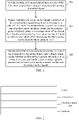
FIG. 1 is a schematic flowchart of a preparation process of a nanomaterial according to some embodiments of the present disclosure. -
FIG. 2 is a schematic structural diagram of a semiconductor device according to some embodiments of the present disclosure. - In order to make the objectives, technical solutions, and advantages of the present disclosure clearer, the present disclosure is further described in detail below in connection with the accompanying drawings and embodiments. Embodiments described herein are only used to explain the present disclosure and are not intended to limit the present disclosure.
- In the description of the present disclosure, a compound and its derivative involved are named according to the International Union of Pure and Applied Chemistry (IUPAC) or Chemical Abstracts Service (CAS, located in Columbus, Ohio). Compound groups involved are described as follows.
- "Alkyl" refers to a saturated chain hydrocarbon group having only carbon and hydrogen, which may have a straight carbon chain and/or a branched carbon chain. Alkyl may include, but is not limited to, methyl, ethyl, propyl, isopropyl, butyl, isobutyl, pentyl, isopentyl, etc. A carbon number of the alkyl group may range from 1 to 5. In some embodiments, the carbon number of the alkyl group may be 1, 2, 3, 4, and 5.
- "Alkoxy" refers to an alkyl group directly bonded to an oxygen atom and may include, but is not limited to, methoxy, ethoxy, propoxy, butoxy, isobutoxy, tert-butoxy, etc. A carbon number of the alkoxy group may range from 1 to 5. In some embodiments, the carbon number of the alkoxy group may be 1, 2, 3, 4, and 5.
- "Hydroxyalkoxy" refers to an alkyl group that is directly bonded to an oxygen atom and has at least one carbon atom that is connected to a hydroxyl group, such as hydroxymethoxy, hydroxyethoxy, hydroxypropoxy, and hydroxybutoxy. A carbon number of the hydroxyalkoxy may range from 1 to 5. In some embodiments, the carbon number of the hydroxyalkoxy may be 1, 2, 3, 4, and 5.
- In order to solve the technical problems and make the technical solutions and beneficial effects of the present disclosure clearer, the present disclosure is further described in detail below in connection with embodiments of the present disclosure. It should be understood that embodiments described here are merely used to explain the present disclosure and are not intended to limit the present disclosure.
- A first aspect of embodiments of the present disclosure provides a nanomaterial. The nanomaterial may include a zinc oxide (ZnO) nanocrystal and a surface ligand bonded to the ZnO nanocrystal. A structure of the surface ligand is shown in Formula 1.

- In Formula 1, R1, R2, and R3 may be independently selected from at least one of an alkyl group, an alkoxy group, a hydroxyalkoxy group, a hydroxyl group, and a hydrogen atom. R4 may be selected from a hydrocarbon group that has a carbon number of 5 to 60. The carbon number of the alkyl group may range from 1 to 5. The carbon number of the alkoxy group may range from 1 to 5. The carbon number of the hydroxyalkoxy group may range from 1 to 5.
- In embodiments of the present disclosure, the nanomaterial includes a ZnO nanocrystal and a surface ligand with a benzoquinone structure as shown in Formula 1 that is bonded to the ZnO nanocrystal. The surface ligand contains a long-chain hydrocarbon group having a carbon number of 5 to 60. On one hand, the long-chain hydrocarbon group having a carbon number of 5 to 60 may increase a distance between adjacent ZnO nanocrystals to prevent the ZnO nanocrystal from agglomeration. Thus, the dispersion performance of the ZnO nanocrystal may be improved, and the stability of the ZnO nanocrystal may be optimized. On another hand, with the benzoquinone structure, a defect state caused by a dangling bond and an oxygen vacancy on the surface of the ZnO nanocrystal may be passivated. The oxygen atom of the benzoquinone structure may have good electron acceptance ability and have an affinity to a molecular chain and an entire molecule. Thus, the molecule may become a good electron supply and acceptance carrier, so that the carrier transport and injection ability of the ZnO nanocrystal may be improved. With the benzoquinone structure, the charge blocking that is caused by the long-chain hydrocarbon group may be reduced. The charge blocking may refer to insulating and blocking effect, by the long-chain hydrocarbon group on the surface of the ZnO nanocrystal, on the electron transport between the adjacent nanocrystals. The electron mobility of the ZnO crystal may be increased. In addition, due to the excellent hydrophobicity of the alkyl chain in the surface ligand molecule, the internal ZnO nanocrystal material may be protected from oxygen and water to a certain degree after the surface ligand is bonded at the surface of the ZnO nanocrystal. Thus, the stability of the device may be improved. In summary, the nanomaterial and the surface ligan of the ZnO nanocrystal of embodiments of the present disclosure may improve the electron mobility of the ZnO nanocrystal and improve the stability of the solution.
- In some embodiments, the nanomaterial may include the ZnO nanocrystal and the surface ligand bonded to the ZnO nanocrystal.
- In some embodiments, R4 may include a saturated or unsaturated hydrocarbon group having 5 to 30 carbon atoms. When the carbon number of R4 is 5 to 30, the surface ligand of the benzoquinone structure may have a suitable chain length. The distance between the adjacent ZnO nanocrystals may be increased, and the ZnO crystal may be prevented from agglomeration. Thus, the dispersion performance of the ZnO nanocrystal may be improved, and the stability of the solution of the ZnO nanocrystal may be improved. Moreover, the insulating and blocking effect caused by the introduction of the long-chain group to the charge transport between the adjacent nanocrystals may be reduced. Thus, the electron mobility of the ZnO nanocrystal may be significantly improved. In addition, the alkyl chain may have excellent hydrophobicity. After the surface ligand is bonded on the surface of the ZnO nanocrystal, the internal ZnO nanocrystal material may be protected from oxygen and water to a certain degree to improve the stability of the device.
- In embodiments of the present disclosure, R1, R2, and R3 may each independently include at least one of an alkyl group, an alkoxy group, a hydroxyalkoxy group, a hydroxyl group, or a hydrogen atom. The alkyl group may be represented as -R. The alkoxy group may be represented as -OR. The hydroxyalkoxy group may be represented as -OROH. R may be the alkyl group. The alkyl chain introduced by R4 may have a relatively long-chain length and excellent hydrophobicity. After R4 is bonded to the surface of the ZnO nanocrystal, the internal ZnO nanocrystal material may be protected from oxygen and water to a certain degree to improve the stability of the device.
- In some embodiments, the alkyl group may include a straight-chain saturated alkyl group having 1 to 5 carbon atoms. At this time, at least one of R1, R2, or R3 may include the straight-chain saturated alkyl group having 1 to 5 carbon atoms. Thus, by protecting the internal ZnO nanocrystal material from oxygen and water to a certain degree, the insulating and blocking effect on the charge transport between adjacent nanocrystals caused by an excessive long chain length may be avoided.
- In some embodiments, the alkoxy group may include a straight-chain saturated alkoxy group having 1 to 4 carbon atoms. At this time, at least one of R1, R2, or R3 includes the straight-chain saturated alkoxy group having 1 to 4 carbon atoms. Thus, by protecting the internal ZnO nanocrystal material from oxygen and water to a certain degree, the insulating and blocking effect on the charge transport between adjacent nanocrystals caused by an excessive long chain length may be avoided.
- In some embodiments, the hydroxyalkoxy group may include a straight-chain saturated hydroxyalkoxy group having 1 to 3 carbon atoms. At least one of R1, R2, or R3 may include the straight-chain saturated group having 1 to 3 carbon atoms. Thus, by protecting the internal ZnO nanocrystal material from oxygen and water to a certain degree, the insulating and blocking effect on the charge transport between adjacent nanocrystals caused by an excessive long chain length may be avoided.
- In some embodiments, a total carbon number of R1 and R2 may be less than 6. The carbon number of R3 may be less than 3. Thus, in the obtained structure of Formula 1, the steric hindrance may be small, and the insulating and blocking effect on the charge transport between the adjacent nanocrystals may be minimum.
- In some embodiments, the surface ligand may include at least one of the following structures.


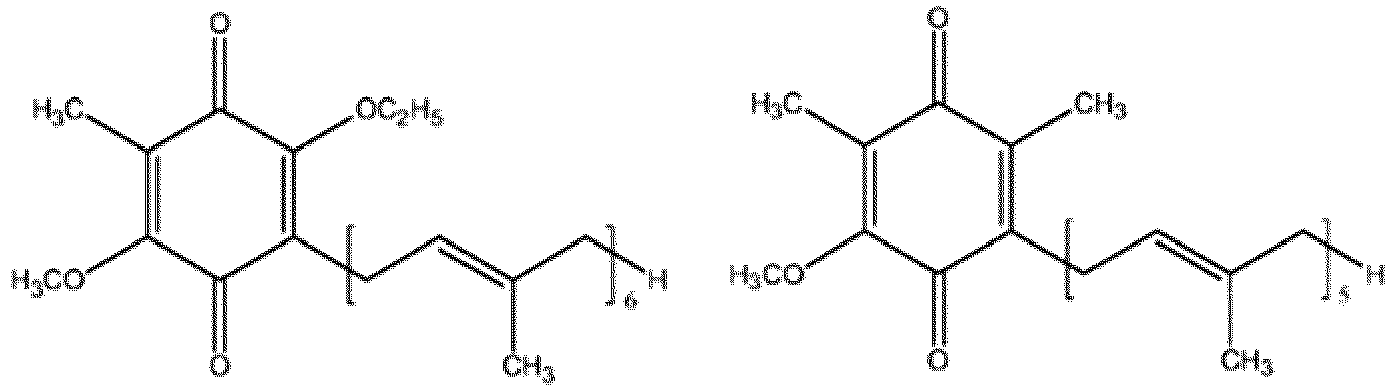


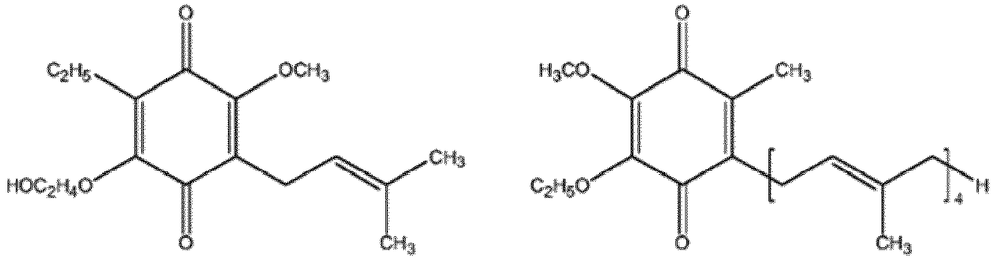

- The surface ligand may have an efficient carrier transport and injection ability. With the surface ligand, the defect on the surface of the ZnO nanocrystal may be passivated. In addition, the hydrocarbyl chain in the ligand molecule may have excellent hydrophobicity and have a shielding effect on water and oxygen. Thus, the stability of the ZnO nanocrystal and the adjacent thin-film layers in the device may be improved.
- In some embodiments, in the nanomaterial, a molar ratio of the ZnO nanocrystal to a surface ligand bonded to the ZnO nanocrystal may range from 1:5 to 1:100. With the molar ratio of the ZnO nanocrystal to the surface ligand bonded at the ZnO nanocrystal being in that range, the surface ligand may be sufficiently bonded to a reaction site on the ZnO nanocrystal to improve the stability of the ZnO nanocrystal, reduce the surface defect on the ZnO nanocrystal, and improve the electron transport performance of the ZnO nanocrystal. When a molar content of the surface ligand bonded to the ZnO nanocrystal is too high, for example, when a molar amount of the ZnO nanocrystal is 1 and the molar content of the surface ligand exceeds 100, the bonding of the surface ligand to the ZnO nanocrystal may not be strong enough, and hence the surface ligand may easily fall off to affect the electron transport performance of the nanomaterial. When the molar content of the surface ligand bonded to the ZnO nanocrystal is too low, for example, when the molar content of the ZnO nanocrystal is 1, and the molar content of the surface ligand is less than 5, the surface ligand may have a limited effect on the stability of the ZnO nanocrystal and the electron transport layer, and hence cannot significantly improve the ZnO nanocrystal.
- The nanomaterial of embodiments of the present disclosure may be prepared by the following method.
- The present disclosure also provides a preparation method of a nanomaterial, including the following steps:
- at S01, providing an initial ZnO nanocrystal solution, a solute of the ZnO nanocrystal solution being a ZnO nanocrystal having a first surface ligand;
- at S02, preparing a solution of a second surface ligand, a structure of the second surface ligand being shown in Formula 1, in which R1, R2, and R3 are independently selected from at least one of an alkyl group, an alkoxy group, a hydroxyalkoxy group, a hydroxyl group, or a hydrogen atom, R4 is selected from a hydrocarbon group having a carbon number of 5 to 60, and the carbon number of the alkyl group, the alkoxy group, and the hydroxyalkoxy group is 1 to 5;

- at S03, mixing the initial ZnO nanocrystal solution and the solution of the second surface ligand solution to cause a displacement reaction between the first surface ligand on the surface of the initial ZnO nanocrystal and the second surface ligand to prepare the ZnO nanocrystal having a surface bonded with the second surface ligand.
- In the preparation method of the nanomaterial of embodiments of the present disclosure, the initial ZnO nanocrystal solution and the surface ligand solution may only need to be mixed to cause the displacement reaction between the first surface ligand on the surface of the initial ZnO nanocrystal and the second surface ligand. Thus, the ZnO nanocrystal with the surface bonded with the second surface ligand may be prepared. The method may have a simple process and a mild condition. With the method, large-scale production may be easily realized. Most importantly, with the nanomaterial prepared by the method, the electron mobility of the ZnO nanocrystal and the solution stability may be improved.
- Specifically, in step S01, the initial ZnO nanocrystal solution may be prepared using, e.g., a solution method. The solute of the ZnO nanocrystal solution may be the ZnO nanocrystal having the first surface ligand. In some embodiments, the first surface ligand may include at least one of an acetate ligand, a hydroxyl ligand, an alkyl ligand, or an alcohol ether ligand. In some embodiments, the first surface ligand may include an acetate ligand and/or a hydroxyl ligand. By selecting the initial ZnO nanocrystal having the acetate ligand and/or the hydroxyl ligand, a ligand replacement rate may be improved in the subsequent ligand replacement reaction with the second surface ligand, and the first surface ligand on the surface of the initial ZnO nanocrystalline may be sufficiently replaced with the second surface ligand.
- In step S02, the solution of the second surface ligand is prepared. The selection of the second surface ligand is described above, which is not repeated here. In some embodiments, in the second organic ligand shown in Formula 1, R4 may include a saturated or unsaturated hydrocarbon group having a carbon number of 5 to 30. In embodiments of the present disclosure, in the first organic ligand shown in Formula 1, R1, R2, and R3 may each include at least one of an alkyl group, an alkoxy group, a hydroxyalkoxy group, a hydroxyl group, or a hydrogen atom. In some embodiments, the alkyl group may include the straight-chain saturated alkyl group having 1 to 5 carbon atoms. In some embodiments, the alkoxy group may include the straight-chain saturated alkoxy group having 1 to 4 carbon atoms. In some embodiments, in the first organic ligand shown in Formula 1, R1, R2, and R3 may each include at least one of an alkyl group, an alkoxy group, a hydroxyalkoxy group, a hydroxyl group, or a hydrogen atom. The hydroxyalkoxy group may include the straight-chain saturated hydroxyalkoxy group having 1 to 3 carbon atoms. In some embodiments, in the first organic ligand shown in Formula 1, at least one of R1, R2, or R3 may include a hydroxyl group or a hydrogen atom.
- In some embodiments, in the first organic ligand shown in Formula 1, the first surface ligand may include at least one of the following structures.


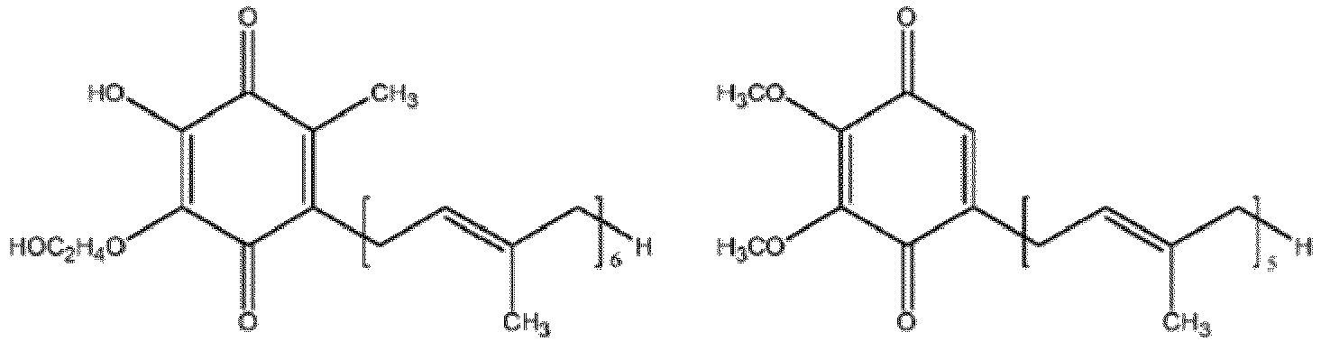


- The first surface ligand may have the efficient carrier transport and injection ability. At the same time, the first surface ligand may be used to passivate the defect on the surface of the ZnO nanocrystal. In addition, the hydrocarbyl chain in the ligand molecule may have excellent hydrophobicity and have a shielding effect on water and oxygen. With the ligand, the stability of the ZnO nanocrystal and the adjacent thin film layers in the device may be improved.
- In step S03, the initial ZnO nanocrystal solution is mixed with the solution of the second surface ligand to cause the displacement reaction between the first surface ligand on the surface of the initial ZnO nanocrystal and the second surface ligand to prepare the ZnO nanocrystal with the surface bonded with the second surface ligand.
- In some embodiments, in mixing the initial ZnO nanocrystal solution and the solution of the second surface ligand, the initial ZnO nanocrystal solution and the second surface ligand solution may be mixed according to a molar ratio of the ZnO nanocrystal to the second surface ligand that ranges from 1:5 to 1:100. With the molar ratio of the initial ZnO nanocrystal to the second surface ligand being within the above range, the second surface ligand may fully replace the first surface ligand on the initial ZnO nanocrystal to form the ZnO nanocrystal bonded with the second surface ligand to improve the stability of the ZnO nanocrystal, reduce the surface defect of the ZnO nanocrystal, and improve the electron transport performance. When the molar content of the surface ligand bonded to the ZnO nanocrystal is too high, for example, when a molar amount of the ZnO nanocrystal is 1 and the molar content of the surface ligand exceeds 100, the bonding of the surface ligand to the ZnO nanocrystal may not be strong enough. The surface ligand may easily fall off to affect the electron transport performance of the nanomaterial. When the molar content of the surface ligand bonded to the ZnO nanocrystal is too low, for example, when the molar content of the ZnO nanocrystal is 1 and the molar content of the surface ligand is less than 5, the surface ligand may not be enough to replace the first surface ligand of the initial ZnO nanocrystal and may not effectively improve the stability of the ZnO nanocrystal and the electron transport layer.
- In some embodiments, in mixing the initial ZnO nanocrystal solution and the solution of the second surface ligand, the mixed solution system may react at a temperature of 50 °C to 250 °C for 20 min to 40 min. If the reaction temperature is too low or the reaction time is too short, the first surface ligand of the initial ZnO nanocrystal may not sufficiently be displaced with the second surface ligand. If the reaction temperature is too high or the reaction time is too long, the second surface ligand may easily be caused to decompose. Thus, the property of the surface ligand bonded to the ZnO nanocrystal may be affected. The purpose of modifying the ZnO nanocrystal may be changed, and even the stability and the electron transport performance of the ZnO nanocrystal may be further reduced.
- As shown in
FIG. 2 , the present disclosure also provides a semiconductor device, including an anode, a cathode, an active layer, and an electron transport layer. The anode and the cathode are arranged oppositely to each other. The active layer is arranged between the anode and the cathode. The electron transport layer is arranged between the active layer and the cathode. A material of the electron transport layer is a nanomaterial. The nanomaterial includes a ZnO nanocrystal and a surface ligand bonded to the ZnO nanocrystal. The structure of the surface ligand is shown in Formula I.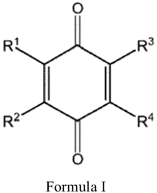
- In Formula I, R1, R2, and R3 may be independently selected from at least one of an alkyl group, an alkoxy group, a hydroxyalkoxy group, a hydroxyl group, or a hydrogen atom. R4 may be selected from a hydrocarbon group having a carbon number of 5 to 60. The carbon number of the alkyl group, the alkoxy group, and the hydroxyalkoxy group may range from 1 to 5.
- In the semiconductor device of embodiments of the present disclosure, the nanomaterial may be used as the electron transport layer. Therefore, the obtained semiconductor device may have relatively good photoelectric efficiency and relatively good stability.
- In some embodiments, the nanomaterial may include the ZnO nanocrystal and the surface ligand bonded to the ZnO nanocrystal.
- The material of the electron transport layer is the nanomaterial. The surface ligand of the nanomaterial is as shown in Formula I. In some embodiments, in the second organic ligand shown in Formula I, R4 may be selected from a saturated or unsaturated hydrocarbon group having 5 to 30 carbon atoms. In embodiments of the present disclosure, in the first organic ligand shown in Formula I, R1, R2, and R3 may be independently selected from at least one of an alkyl group, an alkoxy group, a hydroxyalkoxy group, a hydroxyl group, or a hydrogen atom. In some embodiments, the alkyl group may include the straight-chain saturated alkyl group having 1 to 5 carbon atoms. In some embodiments, the alkoxy group may include the straight-chain saturated alkoxy group having 1 to 4 carbon atoms. In some embodiments, in the first organic ligand shown in Formula I, R1, R2, and R3 may be independently selected from at least one of an alkyl group, an alkoxy group, a hydroxyalkoxy group, a hydroxyl group, or a hydrogen atom. The hydroxyalkoxy group may include the straight-chain saturated hydroxyalkoxy group having 1 to 3 carbon atoms. In some embodiments, in the first organic ligand shown in Formula I, at least one of R1, R2, or R3 may be selected from the hydroxyl group or the hydrogen atom. In some embodiments, the surface ligand may include at least one of the following structures.


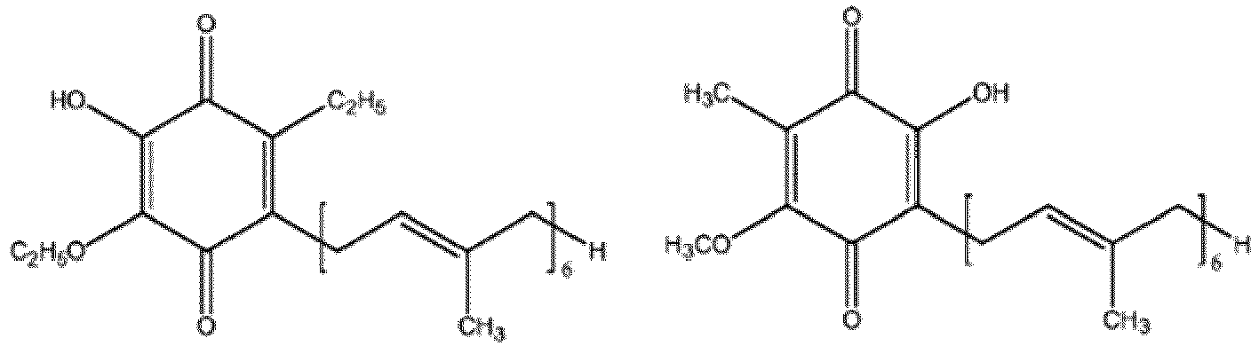


- The surface ligand may have the efficient carrier transport and injection ability. With the surface ligand, the defect on the surface of the ZnO nanocrystal may be passivated. In addition, the hydrocarbyl chain in the ligand molecule may have excellent hydrophobicity and have a shielding effect on water and oxygen. Thus, the stability of the ZnO nanocrystal and the adjacent thin-film layers in the device may be improved.
- In some embodiments, the molar ratio of the ZnO nanocrystal to the surface ligand bonded to the ZnO nanocrystal may range from 1:5 to 1:100.
- Specifically, the semiconductor device may include a solar cell (the device absorbs light from the active layer, such as a perovskite solar cell) or a light-emitting device (the device emits light from a top electrode or a bottom electrode, and the active layer is the light-emitting layer). In some embodiments, the light-emitting device may include an organic light-emitting diode or a quantum dot light-emitting diode. The quantum dot light-emitting diode may include a perovskite light-emitting diode.
- The light-emitting device of embodiments of the present disclosure may be a forward structure electroluminescent device or an inverted structure electroluminescent device. The forward structure refers to a structure of substrate/anode/active layer/electron transport layer/cathode. The device having a forward structure may further optionally include one or more hole functional layers, such as a hole injection layer, a hole transport layer, and/or an electron blocking layer, that is arranged between the anode and the quantum dot light-emitting layer. The device having a forward structure may also further optionally include an electron transport layer, an electron injection layer, and/or a hole blocking layer, that is arranged between the electron transport layer and the cathode. The inverted structure is opposite to the forward structure.
- Specifically, the selection of the anode may not be strictly limited. The anode may include, but is not limited to, an indium-doped tin oxide (ITO).
- The material of the active layer may include a quantum dot or organic light-emitting material.
- The cathode may include, for example, metal copper, metal silver, or metal aluminum.
- The material of the hole injection layer may include one of, but is not limited to, poly(3,4-ethylenedioxythiophene)-polystyrene sulfonic acid (PEDOT:PSS) or a derivative (PEDOT:PSS:s-MoO3) of PEDOT:PSS doped with s-MoO3.
- The material of the hole transport layer may include, but is not limited to, poly[(9,9-dioctylfluorenyl-2,7-diyl)-co-(4,4'-(N-(4-sec-butylphenyl)diphenylamine)] (TFB) or poly(9-vinylcarbazole) (PVK).
- The material of the electron transport layer may include, but is not limited to, ZnO or titanium oxide (TiO2).
- In some embodiments, the light-emitting device may further include a packaging layer. The packaging layer may be arranged on the surface of the top electrode (the electrode away from the substrate) or may be arranged on the surface of the entire electroluminescent device.
- Embodiments and comparative examples are described below.
- An electroluminescent diode device may include an anode, a cathode, an active layer, and an electron transport layer. The anode and the cathode may be arranged oppositely to each other. The active layer may be arranged between the anode and the cathode. The electron transport layer may be arranged between the active layer and the cathode. The anode may be an ITO. The cathode may be made of silver. The active layer may be CdSe@ZnS. The material of the electron transport layer may be the nanomaterial. The nanomaterial may include a ZnO nanocrystal and a surface ligand bonded to the ZnO nanocrystal. The structure of the surface ligand is shown in Formula II.

- An electroluminescent diode device may include an anode, a cathode, an active layer, and an electron transport layer. The anode and the cathode may be arranged oppositely to each other. The active layer may be arranged between the anode and the cathode. The electron transport layer may be arranged between the active layer and the cathode. The anode may include an ITO. The material of the cathode may include silver. The active layer may be CdSe@ZnS. The material of the electron transport layer may include a nanomaterial. The nanomaterial may include a ZnO nanocrystal and a surface ligand bonded to the ZnO nanocrystal. The structure of the surface ligand is shown in Formula III.

- An electroluminescent diode device may include an anode, a cathode, an active layer, and an electron transport layer. The anode and the cathode may be arranged oppositely to each other. The active layer may be arranged between the anode and the cathode. The electron transport layer may be arranged between the active layer and the cathode. The anode may include an ITO. The material of the cathode may include silver. The active layer may be CdSe@ZnS. The material of the electron transport layer may include a nanomaterial. The nanomaterial may include a ZnO nanocrystal and a surface ligand bonded to the ZnO nanocrystal. The structure of the surface ligand is shown in Formula IV.

- An electroluminescent diode device may include an anode, a cathode, an active layer, and an electron transport layer. The anode and the cathode may be arranged oppositely to each other. The active layer may be arranged between the anode and the cathode. The electron transport layer may be arranged between the active layer and the cathode. The anode may include an ITO. The material of the cathode may include silver. The active layer may be the CdSe@ZnS quantum dot light-emitting layer. The material of the electron transport layer may include a nanomaterial. The nanomaterial may include a ZnO nanocrystal and a hydroxyl ligand bonded to the ZnO nanocrystal.
- The efficiency tests are performed on the electroluminescent diode devices of Examples 1 to 3 and Comparative Example 1. The stability of the devices may be monitored. The devices are packaged under a same condition. By isolating the influence of the external environment on the devices, the external quantum efficiency (EQE) from day 1 to day 90 may be monitored after the devices are packaged. The EQE may be measured by an EQE optical test device.
- The test results are shown in Table 1.
Table 1 Item Group External Quantum Efficiency (EQE) /(%) Day 1 Day 10 Day 30 Day 60 Day 90 Comparative Example 1 5.6 5.8 4.9 3.7 3.0 Embodiment 1 8.7 8.4 8.2 8.1 7.9 Embodiment 2 9.3 9.5 9.2 9.1 9.0 Embodiment 3 9.3 9.2 8.9 9.2 8.9 - As shown in Table 1, the EQE of the electroluminescent diode devices of Examples 1 to 3 of the present disclosure is significantly improved compared with Comparative Example 1. The stability of the device efficiency in 90 days is maintained at 90% or above (the percentage of a ratio between the EQE of day 90 and the EQE of day 1). Thus, with the selected ligand of the present disclosure, the electron mobility and the stability of the ZnO nanocrystal may be improved to improve the light-emitting efficiency and the device stability of the electroluminescent devices.
- The above are merely some embodiments of the present disclosure and are not intended to limit the present disclosure. For those skilled in the art, various modifications and changes may be made to the present disclosure. Any modifications, equivalent replacements, and improvements within the spirit and principle of the present application should be within the scope of the claims of the present application.
Claims (22)
- A nanomaterial comprising a ZnO nanocrystal and a surface ligand bonded to the ZnO
nanocrystal, the surface ligand having a structure as shown in Formula 1,
- The nanomaterial according to claim 1, wherein the nanomaterial is composed of the ZnO nanocrystal and the surface ligand bonded to the ZnO nanocrystal.
- The nanomaterial according to claim 1 or 2, wherein R4 is selected from a saturated or unsaturated hydrocarbon group having 5 to 30 carbon atoms.
- The nanomaterial according to claim 1 or 2, wherein:the alkyl group is selected from a straight-chain saturated alkyl group having 1 to 5 carbon atoms;the alkoxy group is selected from a straight-chain saturated alkoxy group having 1 to 4 carbon atoms; orthe hydroxyalkoxy group is selected from a straight-chain saturated hydroxyalkoxy group having 1 to 3 carbon atoms.
- The nanomaterial according to claim 1 or 2, wherein a total carbon number of R1 and R2 is less than 6 and a carbon number of R3 is less than 3.
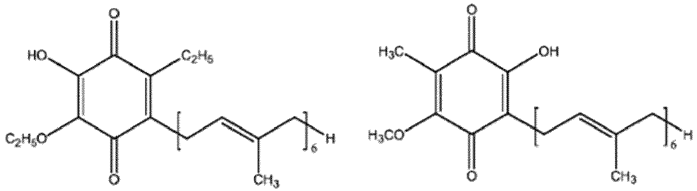
- The nanomaterial according to claim 1 or 2, wherein the surface ligand is selected from at least one of structures of




- The nanomaterial according to claim 1 or 2, wherein, in the nanomaterial, a molar ratio of the ZnO nanocrystal to the surface ligand ranges from 1:5 to 1:100.
- A preparation method of a nanomaterial comprising: providing an initial ZnO nanocrystal solution, a solute of the initial ZnO nanocrystal solution including a ZnO nanocrystal having a first surface ligand, preparing a solution of a second surface ligand, the second surface ligand having a structure as shown in Formula 1,

- The preparation method of the nanomaterial according to claim 8, wherein:R4 is selected from a saturated or unsaturated hydrocarbon group having 5 to 30 carbon atoms; orthe alkyl group is selected from a straight-chain saturated alkyl group having 1 to 5 carbon atoms; orthe alkoxy group is selected from a straight-chain saturated alkoxy group having 1 to 4 carbon atoms; orthe hydroxyalkoxy group is selected from a straight-chain saturated hydroxyalkoxy group having 1 to 3 carbon atoms.
- The preparation method of the nanomaterial according to claim 9, wherein a total carbon number of R1 and R2 is less than 6 and a carbon number of R3 is less than 3.
- The preparation method of the nanomaterial according to claim 9, wherein the surface ligand is selected from at least one of structures of


- The preparation method of the nanomaterial according to any one of claims 8-11, wherein mixing the initial ZnO nanocrystal solution and the solution of the second surface ligand includes mixing the initial ZnO nanocrystal solution and the first surface ligand solution according to a molar ratio of the ZnO nanocrystal to the second surface ligand ranging from 1:5 to 1:100.
- The preparation method of the nanomaterial according to any one of claims 8 to 11, wherein the first surface ligand is selected from at least one of an acetate ligand, a hydroxyl ligand, an alkyl ligand, or an alcohol ether ligand.
- The preparation method of the nanomaterial according to claim 13, wherein the first surface ligand is selected from the acetate ligand or hydroxyl ligand.
- The preparation method of the nanomaterial according to any one of claims 8 to 11 and 14, wherein mixing the initial ZnO nanocrystal solution and the solution of the second surface ligand includes allowing a mixed solution system of the initial ZnO nanocrystal solution and the solution of the second surface ligand to react at a temperature of 50 °C to 250 °C for 20 min to 40 min.
- A semiconductor device comprising an anode and a cathode arranged oppositely to each other, an active layer arranged between the anode and the cathode, and an electron transport layer arranged between the active layer and the cathode, a material of the electron transport layer including a nanomaterial, the nanomaterial including a ZnO nanocrystal and a surface ligand bonded to the ZnO nanocrystal, and the surface ligand having a structure as shown in Formula 1,

- The semiconductor device according to claim 16, wherein the nanomaterial is composed of the ZnO nanocrystal and the surface ligand bonded to the ZnO nanocrystal.
- The semiconductor device according to claim 16 or 17, wherein R4 is selected from a saturated or unsaturated hydrocarbon group having 5 to 30 carbon atoms.
- The semiconductor device according to claim 16 or 17, wherein:the alkyl group is selected from a straight-chain saturated alkyl group having 1 to 5 carbon atoms; orthe alkoxy group is selected from a straight-chain saturated alkoxy group having 1 to 4 carbon atoms; orthe hydroxyalkoxy group is selected from a straight-chain saturated hydroxyalkoxy group having 1 to 3 carbon atoms.
- The semiconductor device according to claim 16 or 17, wherein a total carbon number of R1 and R2 is less than 6 and a carbon number of R3 is less than 3.
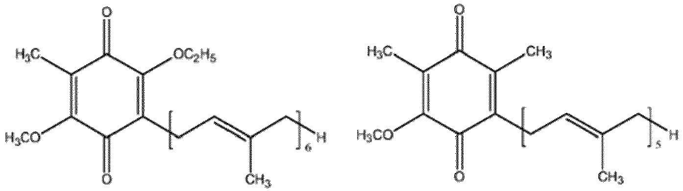
- The semiconductor device according to claim 16 or 17, wherein the surface ligand is selected from at least one of structures of




- The nanomaterial according to claim 16 or 17, wherein, in the nanomaterial, a molar ratio of the ZnO nanocrystal to the surface ligand ranges from 1:5 to 1:100.
Applications Claiming Priority (2)
| Application Number | Priority Date | Filing Date | Title |
|---|---|---|---|
| CN201911384737.7A CN113054121B (en) | 2019-12-28 | 2019-12-28 | Nano material, preparation method thereof and semiconductor device |
| PCT/CN2020/138638 WO2021129665A1 (en) | 2019-12-28 | 2020-12-23 | Nanomaterial and preparation method therefor, and semiconductor device |
Publications (3)
| Publication Number | Publication Date |
|---|---|
| EP4084106A1 true EP4084106A1 (en) | 2022-11-02 |
| EP4084106A4 EP4084106A4 (en) | 2023-04-26 |
| EP4084106B1 EP4084106B1 (en) | 2024-02-07 |
Family
ID=76507683
Family Applications (1)
| Application Number | Title | Priority Date | Filing Date |
|---|---|---|---|
| EP20906671.1A Active EP4084106B1 (en) | 2019-12-28 | 2020-12-23 | Nanomaterial and preparation method therefor, and semiconductor device |
Country Status (4)
| Country | Link |
|---|---|
| US (1) | US12232339B2 (en) |
| EP (1) | EP4084106B1 (en) |
| CN (1) | CN113054121B (en) |
| WO (1) | WO2021129665A1 (en) |
Families Citing this family (1)
| Publication number | Priority date | Publication date | Assignee | Title |
|---|---|---|---|---|
| CN115701263A (en) * | 2021-07-26 | 2023-02-07 | 北京京东方技术开发有限公司 | Electron transport material, electroluminescence device and its preparation method, display device |
Family Cites Families (17)
| Publication number | Priority date | Publication date | Assignee | Title |
|---|---|---|---|---|
| US8007757B2 (en) * | 2006-05-17 | 2011-08-30 | The Board Of Trustees Of The University Of Arkansas | Multi-dimensional complex nanocrystal structures and methods of making same |
| KR20170096241A (en) * | 2008-09-23 | 2017-08-23 | 라보라토리 스킨 케어, 인크. | Active agent loaded uniform, rigid, spherical, nanoporous calcium phosphate particles and methods of making and using the same |
| KR101173105B1 (en) * | 2010-05-24 | 2012-08-14 | 한국과학기술원 | Organic light emitting element |
| TW201245359A (en) * | 2011-03-17 | 2012-11-16 | Sumitomo Chemical Co | Metal complex composition and its mixture |
| JP5750165B2 (en) * | 2011-10-17 | 2015-07-15 | 住友化学株式会社 | Compound |
| CN103855307A (en) * | 2014-03-14 | 2014-06-11 | 国家纳米科学中心 | Perovskite solar battery and preparing method thereof |
| WO2017010398A1 (en) * | 2015-07-16 | 2017-01-19 | ソニー株式会社 | Photoelectric conversion element, manufacturing method of photoelectric conversion element, and imaging apparatus |
| US10983433B2 (en) | 2015-08-21 | 2021-04-20 | Samsung Electronics Co., Ltd. | Photosensitive compositions, preparation methods thereof, and quantum dot polymer composite prepared therefrom |
| GB2551501A (en) | 2016-06-17 | 2017-12-27 | Sumitomo Chemical Co | Nanoparticles |
| CN106450021A (en) * | 2016-11-24 | 2017-02-22 | 南方科技大学 | Organic electroluminescent device and preparation method thereof |
| WO2018103747A1 (en) | 2016-12-08 | 2018-06-14 | 广州华睿光电材料有限公司 | Polymer and electroluminescent device |
| CN108264900A (en) | 2016-12-30 | 2018-07-10 | Tcl集团股份有限公司 | A kind of quantum dot composite material, preparation method and semiconductor devices |
| CN106601926B (en) * | 2016-12-30 | 2019-04-19 | 固安翌光科技有限公司 | Transparent inversion OLED device and preparation method thereof |
| CN108735906B (en) * | 2017-04-20 | 2020-08-18 | Tcl科技集团股份有限公司 | Acrylate copolymer modified metal oxide, QLED and preparation method |
| CN109994620A (en) * | 2017-12-29 | 2019-07-09 | Tcl集团股份有限公司 | Electron-transport film and its preparation method and application |
| CN110484233B (en) * | 2018-04-03 | 2022-08-02 | 浙江大学 | Zinc oxide nanocrystal, zinc oxide nanocrystal composition, preparation method of zinc oxide nanocrystal composition and electroluminescent device |
| JP7474519B2 (en) * | 2018-10-17 | 2024-04-25 | ザ・ユニバーシティ・オブ・シカゴ | Photoactive inorganic anion-capped inorganic nanocrystals |
-
2019
- 2019-12-28 CN CN201911384737.7A patent/CN113054121B/en active Active
-
2020
- 2020-12-23 WO PCT/CN2020/138638 patent/WO2021129665A1/en not_active Ceased
- 2020-12-23 EP EP20906671.1A patent/EP4084106B1/en active Active
-
2022
- 2022-06-13 US US17/838,701 patent/US12232339B2/en active Active
Also Published As
| Publication number | Publication date |
|---|---|
| CN113054121A (en) | 2021-06-29 |
| CN113054121B (en) | 2022-07-05 |
| US20220302401A1 (en) | 2022-09-22 |
| US12232339B2 (en) | 2025-02-18 |
| EP4084106A4 (en) | 2023-04-26 |
| WO2021129665A1 (en) | 2021-07-01 |
| EP4084106B1 (en) | 2024-02-07 |
Similar Documents
| Publication | Publication Date | Title |
|---|---|---|
| Guvenc et al. | Gd3+-doped α-CsPbI3 nanocrystals with better phase stability and optical properties | |
| Heo et al. | Bright lead-free inorganic CsSnBr3 perovskite light-emitting diodes | |
| Ducinskas et al. | Unravelling the behavior of Dion–Jacobson layered hybrid perovskites in humid environments | |
| CN111740033B (en) | Near-infrared perovskite light-emitting diode and preparation method thereof | |
| Xie et al. | Operational stability issues and challenges in metal halide perovskite light-emitting diodes | |
| EP3734679A1 (en) | Electronic transmission thin film, preparation method therefor and application thereof | |
| CN113903865B (en) | Zinc oxide nano material, preparation method thereof and luminescent device | |
| Li et al. | Enhancing the efficiency and stability of CsPbI3 nanocrystal-based light-emitting diodes through ligand engineering with octylamine | |
| Liu et al. | Strategies for the preparation of high-performance inorganic mixed-halide perovskite solar cells | |
| Chung et al. | Effective passivation of perovkiste grain boundaries by a carboxylated polythoiphene for bright and stable Pure-Red perovskite light emitting diodes | |
| US20240246831A1 (en) | Method for preparing tin oxide nanoparticles dispersed in alcohol solvent, and use thereof | |
| CN113493219A (en) | Tin dioxide quantum dot material, preparation method thereof and photoelectric device | |
| CN113838985B (en) | Zinc oxide nano material, preparation method thereof and luminescent device | |
| US12232339B2 (en) | Nanomaterial, preparation method thereof, and semiconductor device | |
| WO2021136044A1 (en) | Quantum dot light-emitting diode and manufacturing method therefor | |
| Bao et al. | Perovskite/organic hybrid white light-emitting diodes with excellent CIE chromaticity coordinate | |
| Yu et al. | Frontiers in Green Perovskite Light‐Emitting Diodes | |
| CN212542486U (en) | Near-infrared perovskite light emitting diode | |
| CN113707777B (en) | Composite materials and preparation methods thereof, light-emitting devices | |
| KR20240006990A (en) | Metal Oxide Nanoparticles and Quantum Dot Light-Emitting Diode Comprising the Same | |
| CN113130790B (en) | Nano material, preparation method thereof and quantum dot light-emitting diode | |
| Chang et al. | High-Performance Quasi-Two-Dimensional CsPbBr2. 1Cl0. 9: PEABr Perovskite Sky-Blue LEDs with an Interface Modification Layer | |
| US12575248B2 (en) | Zinc oxide nanomaterial and preparation method thereof and semiconductor device | |
| CN109970356B (en) | Zinc oxide nano material, preparation method thereof and luminescent device | |
| EP4131448B1 (en) | Nanomaterial, light emitting diode device, and preparation method therefor |
Legal Events
| Date | Code | Title | Description |
|---|---|---|---|
| STAA | Information on the status of an ep patent application or granted ep patent |
Free format text: STATUS: THE INTERNATIONAL PUBLICATION HAS BEEN MADE |
|
| PUAI | Public reference made under article 153(3) epc to a published international application that has entered the european phase |
Free format text: ORIGINAL CODE: 0009012 |
|
| STAA | Information on the status of an ep patent application or granted ep patent |
Free format text: STATUS: REQUEST FOR EXAMINATION WAS MADE |
|
| 17P | Request for examination filed |
Effective date: 20220628 |
|
| AK | Designated contracting states |
Kind code of ref document: A1 Designated state(s): AL AT BE BG CH CY CZ DE DK EE ES FI FR GB GR HR HU IE IS IT LI LT LU LV MC MK MT NL NO PL PT RO RS SE SI SK SM TR |
|
| REG | Reference to a national code |
Ref country code: DE Ref legal event code: R079 Free format text: PREVIOUS MAIN CLASS: H01L0051500000 Ipc: H10K0050160000 Ref document number: 602020025478 Country of ref document: DE |
|
| DAV | Request for validation of the european patent (deleted) | ||
| DAX | Request for extension of the european patent (deleted) | ||
| A4 | Supplementary search report drawn up and despatched |
Effective date: 20230328 |
|
| RIC1 | Information provided on ipc code assigned before grant |
Ipc: H10K 50/115 20230101ALN20230322BHEP Ipc: C09C 1/04 20060101ALI20230322BHEP Ipc: C01G 9/02 20060101ALI20230322BHEP Ipc: B82Y 40/00 20110101ALI20230322BHEP Ipc: B82Y 30/00 20110101ALI20230322BHEP Ipc: B82Y 10/00 20110101ALI20230322BHEP Ipc: H10K 50/16 20230101AFI20230322BHEP |
|
| RIC1 | Information provided on ipc code assigned before grant |
Ipc: H10K 50/115 20230101ALN20230720BHEP Ipc: C09C 1/04 20060101ALI20230720BHEP Ipc: C01G 9/02 20060101ALI20230720BHEP Ipc: B82Y 40/00 20110101ALI20230720BHEP Ipc: B82Y 30/00 20110101ALI20230720BHEP Ipc: B82Y 10/00 20110101ALI20230720BHEP Ipc: H10K 50/16 20230101AFI20230720BHEP |
|
| GRAP | Despatch of communication of intention to grant a patent |
Free format text: ORIGINAL CODE: EPIDOSNIGR1 |
|
| STAA | Information on the status of an ep patent application or granted ep patent |
Free format text: STATUS: GRANT OF PATENT IS INTENDED |
|
| RIC1 | Information provided on ipc code assigned before grant |
Ipc: H10K 50/115 20230101ALN20230811BHEP Ipc: C09C 1/04 20060101ALI20230811BHEP Ipc: C01G 9/02 20060101ALI20230811BHEP Ipc: B82Y 40/00 20110101ALI20230811BHEP Ipc: B82Y 30/00 20110101ALI20230811BHEP Ipc: B82Y 10/00 20110101ALI20230811BHEP Ipc: H10K 50/16 20230101AFI20230811BHEP |
|
| RIC1 | Information provided on ipc code assigned before grant |
Ipc: H10K 50/115 20230101ALN20230825BHEP Ipc: C09C 1/04 20060101ALI20230825BHEP Ipc: C01G 9/02 20060101ALI20230825BHEP Ipc: B82Y 40/00 20110101ALI20230825BHEP Ipc: B82Y 30/00 20110101ALI20230825BHEP Ipc: B82Y 10/00 20110101ALI20230825BHEP Ipc: H10K 50/16 20230101AFI20230825BHEP |
|
| INTG | Intention to grant announced |
Effective date: 20230912 |
|
| GRAS | Grant fee paid |
Free format text: ORIGINAL CODE: EPIDOSNIGR3 |
|
| GRAA | (expected) grant |
Free format text: ORIGINAL CODE: 0009210 |
|
| STAA | Information on the status of an ep patent application or granted ep patent |
Free format text: STATUS: THE PATENT HAS BEEN GRANTED |
|
| AK | Designated contracting states |
Kind code of ref document: B1 Designated state(s): AL AT BE BG CH CY CZ DE DK EE ES FI FR GB GR HR HU IE IS IT LI LT LU LV MC MK MT NL NO PL PT RO RS SE SI SK SM TR |
|
| REG | Reference to a national code |
Ref country code: GB Ref legal event code: FG4D |
|
| REG | Reference to a national code |
Ref country code: CH Ref legal event code: EP |
|
| REG | Reference to a national code |
Ref country code: IE Ref legal event code: FG4D |
|
| REG | Reference to a national code |
Ref country code: DE Ref legal event code: R096 Ref document number: 602020025478 Country of ref document: DE |
|
| REG | Reference to a national code |
Ref country code: LT Ref legal event code: MG9D |
|
| REG | Reference to a national code |
Ref country code: NL Ref legal event code: MP Effective date: 20240207 |
|
| PG25 | Lapsed in a contracting state [announced via postgrant information from national office to epo] |
Ref country code: IS Free format text: LAPSE BECAUSE OF FAILURE TO SUBMIT A TRANSLATION OF THE DESCRIPTION OR TO PAY THE FEE WITHIN THE PRESCRIBED TIME-LIMIT Effective date: 20240607 |
|
| PG25 | Lapsed in a contracting state [announced via postgrant information from national office to epo] |
Ref country code: LT Free format text: LAPSE BECAUSE OF FAILURE TO SUBMIT A TRANSLATION OF THE DESCRIPTION OR TO PAY THE FEE WITHIN THE PRESCRIBED TIME-LIMIT Effective date: 20240207 |
|
| PG25 | Lapsed in a contracting state [announced via postgrant information from national office to epo] |
Ref country code: GR Free format text: LAPSE BECAUSE OF FAILURE TO SUBMIT A TRANSLATION OF THE DESCRIPTION OR TO PAY THE FEE WITHIN THE PRESCRIBED TIME-LIMIT Effective date: 20240508 |
|
| REG | Reference to a national code |
Ref country code: AT Ref legal event code: MK05 Ref document number: 1656178 Country of ref document: AT Kind code of ref document: T Effective date: 20240207 |
|
| PG25 | Lapsed in a contracting state [announced via postgrant information from national office to epo] |
Ref country code: RS Free format text: LAPSE BECAUSE OF FAILURE TO SUBMIT A TRANSLATION OF THE DESCRIPTION OR TO PAY THE FEE WITHIN THE PRESCRIBED TIME-LIMIT Effective date: 20240507 Ref country code: HR Free format text: LAPSE BECAUSE OF FAILURE TO SUBMIT A TRANSLATION OF THE DESCRIPTION OR TO PAY THE FEE WITHIN THE PRESCRIBED TIME-LIMIT Effective date: 20240207 Ref country code: NL Free format text: LAPSE BECAUSE OF FAILURE TO SUBMIT A TRANSLATION OF THE DESCRIPTION OR TO PAY THE FEE WITHIN THE PRESCRIBED TIME-LIMIT Effective date: 20240207 |
|
| PG25 | Lapsed in a contracting state [announced via postgrant information from national office to epo] |
Ref country code: ES Free format text: LAPSE BECAUSE OF FAILURE TO SUBMIT A TRANSLATION OF THE DESCRIPTION OR TO PAY THE FEE WITHIN THE PRESCRIBED TIME-LIMIT Effective date: 20240207 |
|
| PG25 | Lapsed in a contracting state [announced via postgrant information from national office to epo] |
Ref country code: AT Free format text: LAPSE BECAUSE OF FAILURE TO SUBMIT A TRANSLATION OF THE DESCRIPTION OR TO PAY THE FEE WITHIN THE PRESCRIBED TIME-LIMIT Effective date: 20240207 |
|
| PG25 | Lapsed in a contracting state [announced via postgrant information from national office to epo] |
Ref country code: RS Free format text: LAPSE BECAUSE OF FAILURE TO SUBMIT A TRANSLATION OF THE DESCRIPTION OR TO PAY THE FEE WITHIN THE PRESCRIBED TIME-LIMIT Effective date: 20240507 Ref country code: NO Free format text: LAPSE BECAUSE OF FAILURE TO SUBMIT A TRANSLATION OF THE DESCRIPTION OR TO PAY THE FEE WITHIN THE PRESCRIBED TIME-LIMIT Effective date: 20240507 Ref country code: NL Free format text: LAPSE BECAUSE OF FAILURE TO SUBMIT A TRANSLATION OF THE DESCRIPTION OR TO PAY THE FEE WITHIN THE PRESCRIBED TIME-LIMIT Effective date: 20240207 Ref country code: LT Free format text: LAPSE BECAUSE OF FAILURE TO SUBMIT A TRANSLATION OF THE DESCRIPTION OR TO PAY THE FEE WITHIN THE PRESCRIBED TIME-LIMIT Effective date: 20240207 Ref country code: IS Free format text: LAPSE BECAUSE OF FAILURE TO SUBMIT A TRANSLATION OF THE DESCRIPTION OR TO PAY THE FEE WITHIN THE PRESCRIBED TIME-LIMIT Effective date: 20240607 Ref country code: HR Free format text: LAPSE BECAUSE OF FAILURE TO SUBMIT A TRANSLATION OF THE DESCRIPTION OR TO PAY THE FEE WITHIN THE PRESCRIBED TIME-LIMIT Effective date: 20240207 Ref country code: GR Free format text: LAPSE BECAUSE OF FAILURE TO SUBMIT A TRANSLATION OF THE DESCRIPTION OR TO PAY THE FEE WITHIN THE PRESCRIBED TIME-LIMIT Effective date: 20240508 Ref country code: FI Free format text: LAPSE BECAUSE OF FAILURE TO SUBMIT A TRANSLATION OF THE DESCRIPTION OR TO PAY THE FEE WITHIN THE PRESCRIBED TIME-LIMIT Effective date: 20240207 Ref country code: ES Free format text: LAPSE BECAUSE OF FAILURE TO SUBMIT A TRANSLATION OF THE DESCRIPTION OR TO PAY THE FEE WITHIN THE PRESCRIBED TIME-LIMIT Effective date: 20240207 Ref country code: BG Free format text: LAPSE BECAUSE OF FAILURE TO SUBMIT A TRANSLATION OF THE DESCRIPTION OR TO PAY THE FEE WITHIN THE PRESCRIBED TIME-LIMIT Effective date: 20240207 Ref country code: AT Free format text: LAPSE BECAUSE OF FAILURE TO SUBMIT A TRANSLATION OF THE DESCRIPTION OR TO PAY THE FEE WITHIN THE PRESCRIBED TIME-LIMIT Effective date: 20240207 |
|
| PG25 | Lapsed in a contracting state [announced via postgrant information from national office to epo] |
Ref country code: PL Free format text: LAPSE BECAUSE OF FAILURE TO SUBMIT A TRANSLATION OF THE DESCRIPTION OR TO PAY THE FEE WITHIN THE PRESCRIBED TIME-LIMIT Effective date: 20240207 Ref country code: PT Free format text: LAPSE BECAUSE OF FAILURE TO SUBMIT A TRANSLATION OF THE DESCRIPTION OR TO PAY THE FEE WITHIN THE PRESCRIBED TIME-LIMIT Effective date: 20240607 |
|
| PG25 | Lapsed in a contracting state [announced via postgrant information from national office to epo] |
Ref country code: SE Free format text: LAPSE BECAUSE OF FAILURE TO SUBMIT A TRANSLATION OF THE DESCRIPTION OR TO PAY THE FEE WITHIN THE PRESCRIBED TIME-LIMIT Effective date: 20240207 Ref country code: PT Free format text: LAPSE BECAUSE OF FAILURE TO SUBMIT A TRANSLATION OF THE DESCRIPTION OR TO PAY THE FEE WITHIN THE PRESCRIBED TIME-LIMIT Effective date: 20240607 Ref country code: PL Free format text: LAPSE BECAUSE OF FAILURE TO SUBMIT A TRANSLATION OF THE DESCRIPTION OR TO PAY THE FEE WITHIN THE PRESCRIBED TIME-LIMIT Effective date: 20240207 Ref country code: LV Free format text: LAPSE BECAUSE OF FAILURE TO SUBMIT A TRANSLATION OF THE DESCRIPTION OR TO PAY THE FEE WITHIN THE PRESCRIBED TIME-LIMIT Effective date: 20240207 |
|
| PG25 | Lapsed in a contracting state [announced via postgrant information from national office to epo] |
Ref country code: DK Free format text: LAPSE BECAUSE OF FAILURE TO SUBMIT A TRANSLATION OF THE DESCRIPTION OR TO PAY THE FEE WITHIN THE PRESCRIBED TIME-LIMIT Effective date: 20240207 |
|
| PG25 | Lapsed in a contracting state [announced via postgrant information from national office to epo] |
Ref country code: SM Free format text: LAPSE BECAUSE OF FAILURE TO SUBMIT A TRANSLATION OF THE DESCRIPTION OR TO PAY THE FEE WITHIN THE PRESCRIBED TIME-LIMIT Effective date: 20240207 |
|
| PG25 | Lapsed in a contracting state [announced via postgrant information from national office to epo] |
Ref country code: CZ Free format text: LAPSE BECAUSE OF FAILURE TO SUBMIT A TRANSLATION OF THE DESCRIPTION OR TO PAY THE FEE WITHIN THE PRESCRIBED TIME-LIMIT Effective date: 20240207 Ref country code: EE Free format text: LAPSE BECAUSE OF FAILURE TO SUBMIT A TRANSLATION OF THE DESCRIPTION OR TO PAY THE FEE WITHIN THE PRESCRIBED TIME-LIMIT Effective date: 20240207 |
|
| PG25 | Lapsed in a contracting state [announced via postgrant information from national office to epo] |
Ref country code: SK Free format text: LAPSE BECAUSE OF FAILURE TO SUBMIT A TRANSLATION OF THE DESCRIPTION OR TO PAY THE FEE WITHIN THE PRESCRIBED TIME-LIMIT Effective date: 20240207 |
|
| PG25 | Lapsed in a contracting state [announced via postgrant information from national office to epo] |
Ref country code: SM Free format text: LAPSE BECAUSE OF FAILURE TO SUBMIT A TRANSLATION OF THE DESCRIPTION OR TO PAY THE FEE WITHIN THE PRESCRIBED TIME-LIMIT Effective date: 20240207 Ref country code: SK Free format text: LAPSE BECAUSE OF FAILURE TO SUBMIT A TRANSLATION OF THE DESCRIPTION OR TO PAY THE FEE WITHIN THE PRESCRIBED TIME-LIMIT Effective date: 20240207 Ref country code: RO Free format text: LAPSE BECAUSE OF FAILURE TO SUBMIT A TRANSLATION OF THE DESCRIPTION OR TO PAY THE FEE WITHIN THE PRESCRIBED TIME-LIMIT Effective date: 20240207 Ref country code: EE Free format text: LAPSE BECAUSE OF FAILURE TO SUBMIT A TRANSLATION OF THE DESCRIPTION OR TO PAY THE FEE WITHIN THE PRESCRIBED TIME-LIMIT Effective date: 20240207 Ref country code: DK Free format text: LAPSE BECAUSE OF FAILURE TO SUBMIT A TRANSLATION OF THE DESCRIPTION OR TO PAY THE FEE WITHIN THE PRESCRIBED TIME-LIMIT Effective date: 20240207 Ref country code: CZ Free format text: LAPSE BECAUSE OF FAILURE TO SUBMIT A TRANSLATION OF THE DESCRIPTION OR TO PAY THE FEE WITHIN THE PRESCRIBED TIME-LIMIT Effective date: 20240207 |
|
| REG | Reference to a national code |
Ref country code: DE Ref legal event code: R097 Ref document number: 602020025478 Country of ref document: DE |
|
| PG25 | Lapsed in a contracting state [announced via postgrant information from national office to epo] |
Ref country code: IT Free format text: LAPSE BECAUSE OF FAILURE TO SUBMIT A TRANSLATION OF THE DESCRIPTION OR TO PAY THE FEE WITHIN THE PRESCRIBED TIME-LIMIT Effective date: 20240207 |
|
| PLBE | No opposition filed within time limit |
Free format text: ORIGINAL CODE: 0009261 |
|
| STAA | Information on the status of an ep patent application or granted ep patent |
Free format text: STATUS: NO OPPOSITION FILED WITHIN TIME LIMIT |
|
| PG25 | Lapsed in a contracting state [announced via postgrant information from national office to epo] |
Ref country code: IT Free format text: LAPSE BECAUSE OF FAILURE TO SUBMIT A TRANSLATION OF THE DESCRIPTION OR TO PAY THE FEE WITHIN THE PRESCRIBED TIME-LIMIT Effective date: 20240207 |
|
| 26N | No opposition filed |
Effective date: 20241108 |
|
| PG25 | Lapsed in a contracting state [announced via postgrant information from national office to epo] |
Ref country code: SI Free format text: LAPSE BECAUSE OF FAILURE TO SUBMIT A TRANSLATION OF THE DESCRIPTION OR TO PAY THE FEE WITHIN THE PRESCRIBED TIME-LIMIT Effective date: 20240207 |
|
| PG25 | Lapsed in a contracting state [announced via postgrant information from national office to epo] |
Ref country code: MC Free format text: LAPSE BECAUSE OF FAILURE TO SUBMIT A TRANSLATION OF THE DESCRIPTION OR TO PAY THE FEE WITHIN THE PRESCRIBED TIME-LIMIT Effective date: 20240207 |
|
| REG | Reference to a national code |
Ref country code: CH Ref legal event code: PL |
|
| PG25 | Lapsed in a contracting state [announced via postgrant information from national office to epo] |
Ref country code: LU Free format text: LAPSE BECAUSE OF NON-PAYMENT OF DUE FEES Effective date: 20241223 |
|
| REG | Reference to a national code |
Ref country code: BE Ref legal event code: MM Effective date: 20241231 |
|
| PG25 | Lapsed in a contracting state [announced via postgrant information from national office to epo] |
Ref country code: BE Free format text: LAPSE BECAUSE OF NON-PAYMENT OF DUE FEES Effective date: 20241231 |
|
| PG25 | Lapsed in a contracting state [announced via postgrant information from national office to epo] |
Ref country code: CH Free format text: LAPSE BECAUSE OF NON-PAYMENT OF DUE FEES Effective date: 20241231 |
|
| PG25 | Lapsed in a contracting state [announced via postgrant information from national office to epo] |
Ref country code: IE Free format text: LAPSE BECAUSE OF NON-PAYMENT OF DUE FEES Effective date: 20241223 |
|
| PGFP | Annual fee paid to national office [announced via postgrant information from national office to epo] |
Ref country code: DE Payment date: 20251211 Year of fee payment: 6 |
|
| PGFP | Annual fee paid to national office [announced via postgrant information from national office to epo] |
Ref country code: GB Payment date: 20251219 Year of fee payment: 6 |
|
| PGFP | Annual fee paid to national office [announced via postgrant information from national office to epo] |
Ref country code: FR Payment date: 20251229 Year of fee payment: 6 |
|
| PG25 | Lapsed in a contracting state [announced via postgrant information from national office to epo] |
Ref country code: CY Free format text: LAPSE BECAUSE OF FAILURE TO SUBMIT A TRANSLATION OF THE DESCRIPTION OR TO PAY THE FEE WITHIN THE PRESCRIBED TIME-LIMIT Effective date: 20240207 |