EP4084053A1 - Semiconductor structure and method for manufacturing semiconductor structure - Google Patents
Semiconductor structure and method for manufacturing semiconductor structure Download PDFInfo
- Publication number
- EP4084053A1 EP4084053A1 EP21863069.7A EP21863069A EP4084053A1 EP 4084053 A1 EP4084053 A1 EP 4084053A1 EP 21863069 A EP21863069 A EP 21863069A EP 4084053 A1 EP4084053 A1 EP 4084053A1
- Authority
- EP
- European Patent Office
- Prior art keywords
- semiconductor structure
- air gap
- conductive
- conductive layer
- via portion
- Prior art date
- Legal status (The legal status is an assumption and is not a legal conclusion. Google has not performed a legal analysis and makes no representation as to the accuracy of the status listed.)
- Granted
Links
Images






Classifications
-
- H—ELECTRICITY
- H10—SEMICONDUCTOR DEVICES; ELECTRIC SOLID-STATE DEVICES NOT OTHERWISE PROVIDED FOR
- H10W—GENERIC PACKAGES, INTERCONNECTIONS, CONNECTORS OR OTHER CONSTRUCTIONAL DETAILS OF DEVICES COVERED BY CLASS H10
- H10W20/00—Interconnections in chips, wafers or substrates
- H10W20/01—Manufacture or treatment
- H10W20/021—Manufacture or treatment of interconnections within wafers or substrates
- H10W20/023—Manufacture or treatment of interconnections within wafers or substrates the interconnections being through-semiconductor vias
-
- H—ELECTRICITY
- H10—SEMICONDUCTOR DEVICES; ELECTRIC SOLID-STATE DEVICES NOT OTHERWISE PROVIDED FOR
- H10W—GENERIC PACKAGES, INTERCONNECTIONS, CONNECTORS OR OTHER CONSTRUCTIONAL DETAILS OF DEVICES COVERED BY CLASS H10
- H10W20/00—Interconnections in chips, wafers or substrates
- H10W20/01—Manufacture or treatment
- H10W20/031—Manufacture or treatment of conductive parts of the interconnections
- H10W20/056—Manufacture or treatment of conductive parts of the interconnections by filling conductive material into holes, grooves or trenches
- H10W20/057—Manufacture or treatment of conductive parts of the interconnections by filling conductive material into holes, grooves or trenches by selectively depositing, e.g. by using selective CVD or plating
-
- H—ELECTRICITY
- H10—SEMICONDUCTOR DEVICES; ELECTRIC SOLID-STATE DEVICES NOT OTHERWISE PROVIDED FOR
- H10W—GENERIC PACKAGES, INTERCONNECTIONS, CONNECTORS OR OTHER CONSTRUCTIONAL DETAILS OF DEVICES COVERED BY CLASS H10
- H10W20/00—Interconnections in chips, wafers or substrates
- H10W20/01—Manufacture or treatment
- H10W20/071—Manufacture or treatment of dielectric parts thereof
- H10W20/072—Manufacture or treatment of dielectric parts thereof of dielectric parts comprising air gaps
-
- H—ELECTRICITY
- H10—SEMICONDUCTOR DEVICES; ELECTRIC SOLID-STATE DEVICES NOT OTHERWISE PROVIDED FOR
- H10W—GENERIC PACKAGES, INTERCONNECTIONS, CONNECTORS OR OTHER CONSTRUCTIONAL DETAILS OF DEVICES COVERED BY CLASS H10
- H10W20/00—Interconnections in chips, wafers or substrates
- H10W20/01—Manufacture or treatment
- H10W20/071—Manufacture or treatment of dielectric parts thereof
- H10W20/074—Manufacture or treatment of dielectric parts thereof of dielectric parts comprising thin functional dielectric layers, e.g. dielectric etch-stop, barrier, capping or liner layers
- H10W20/076—Manufacture or treatment of dielectric parts thereof of dielectric parts comprising thin functional dielectric layers, e.g. dielectric etch-stop, barrier, capping or liner layers in via holes or trenches
-
- H—ELECTRICITY
- H10—SEMICONDUCTOR DEVICES; ELECTRIC SOLID-STATE DEVICES NOT OTHERWISE PROVIDED FOR
- H10W—GENERIC PACKAGES, INTERCONNECTIONS, CONNECTORS OR OTHER CONSTRUCTIONAL DETAILS OF DEVICES COVERED BY CLASS H10
- H10W20/00—Interconnections in chips, wafers or substrates
- H10W20/20—Interconnections within wafers or substrates, e.g. through-silicon vias [TSV]
-
- H—ELECTRICITY
- H10—SEMICONDUCTOR DEVICES; ELECTRIC SOLID-STATE DEVICES NOT OTHERWISE PROVIDED FOR
- H10W—GENERIC PACKAGES, INTERCONNECTIONS, CONNECTORS OR OTHER CONSTRUCTIONAL DETAILS OF DEVICES COVERED BY CLASS H10
- H10W20/00—Interconnections in chips, wafers or substrates
- H10W20/20—Interconnections within wafers or substrates, e.g. through-silicon vias [TSV]
- H10W20/211—Through-semiconductor vias, e.g. TSVs
- H10W20/213—Cross-sectional shapes or dispositions
- H10W20/2134—TSVs extending from the semiconductor wafer into back-end-of-line layers
-
- H—ELECTRICITY
- H10—SEMICONDUCTOR DEVICES; ELECTRIC SOLID-STATE DEVICES NOT OTHERWISE PROVIDED FOR
- H10W—GENERIC PACKAGES, INTERCONNECTIONS, CONNECTORS OR OTHER CONSTRUCTIONAL DETAILS OF DEVICES COVERED BY CLASS H10
- H10W20/00—Interconnections in chips, wafers or substrates
- H10W20/40—Interconnections external to wafers or substrates, e.g. back-end-of-line [BEOL] metallisations or vias connecting to gate electrodes
- H10W20/41—Interconnections external to wafers or substrates, e.g. back-end-of-line [BEOL] metallisations or vias connecting to gate electrodes characterised by their conductive parts
- H10W20/44—Conductive materials thereof
-
- H—ELECTRICITY
- H10—SEMICONDUCTOR DEVICES; ELECTRIC SOLID-STATE DEVICES NOT OTHERWISE PROVIDED FOR
- H10W—GENERIC PACKAGES, INTERCONNECTIONS, CONNECTORS OR OTHER CONSTRUCTIONAL DETAILS OF DEVICES COVERED BY CLASS H10
- H10W20/00—Interconnections in chips, wafers or substrates
- H10W20/40—Interconnections external to wafers or substrates, e.g. back-end-of-line [BEOL] metallisations or vias connecting to gate electrodes
- H10W20/45—Interconnections external to wafers or substrates, e.g. back-end-of-line [BEOL] metallisations or vias connecting to gate electrodes characterised by their insulating parts
- H10W20/46—Interconnections external to wafers or substrates, e.g. back-end-of-line [BEOL] metallisations or vias connecting to gate electrodes characterised by their insulating parts comprising air gaps
-
- H—ELECTRICITY
- H10—SEMICONDUCTOR DEVICES; ELECTRIC SOLID-STATE DEVICES NOT OTHERWISE PROVIDED FOR
- H10W—GENERIC PACKAGES, INTERCONNECTIONS, CONNECTORS OR OTHER CONSTRUCTIONAL DETAILS OF DEVICES COVERED BY CLASS H10
- H10W20/00—Interconnections in chips, wafers or substrates
- H10W20/40—Interconnections external to wafers or substrates, e.g. back-end-of-line [BEOL] metallisations or vias connecting to gate electrodes
- H10W20/495—Capacitive arrangements or effects of, or between wiring layers
-
- H—ELECTRICITY
- H10—SEMICONDUCTOR DEVICES; ELECTRIC SOLID-STATE DEVICES NOT OTHERWISE PROVIDED FOR
- H10W—GENERIC PACKAGES, INTERCONNECTIONS, CONNECTORS OR OTHER CONSTRUCTIONAL DETAILS OF DEVICES COVERED BY CLASS H10
- H10W20/00—Interconnections in chips, wafers or substrates
- H10W20/40—Interconnections external to wafers or substrates, e.g. back-end-of-line [BEOL] metallisations or vias connecting to gate electrodes
- H10W20/41—Interconnections external to wafers or substrates, e.g. back-end-of-line [BEOL] metallisations or vias connecting to gate electrodes characterised by their conductive parts
- H10W20/435—Cross-sectional shapes or dispositions of interconnections
Definitions
- This disclosure relates to the field of semiconductor technology, and more particularly, to a semiconductor structure and a method for manufacturing the semiconductor structure.
- the metal conductive material filled in the via will affect the surrounding lattice of the via portion during the thermal expansion process, or directly cause the deformation of the upper metal layer, thereby affecting the performance of the semiconductor structure.
- the disclosure provides a semiconductor structure and a method for manufacturing the semiconductor structure, so as to improve the performance of the semiconductor structure.
- a semiconductor structure including:
- a method for manufacturing a semiconductor structure including:
- the semiconductor structure of the disclosure includes the base and the conductive portion that includes the via portion and the first conductive layer.
- the semiconductor structure includes a base 10 and a conductive portion 20 arranged in the base 10, where the conductive portion 20 includes a via portion 21 and a first conductive layer 22.
- the first conductive layer 22 is connected with the via portion 21 and arranged above the via portion 21.
- An air gap 11 is arranged in the base 10, and one end of the air gap is configured to expose the conductive portion 20.
- the semiconductor structure of the disclosure includes the base 10 and the conductive portion 20 that includes the via portion 21 and the first conductive layer 22.
- the semiconductor structure of the disclosure includes the base 10 and the conductive portion 20 that includes the via portion 21 and the first conductive layer 22.
- FIG. 1 in a normal state of the conductive portion 20, there may be no conductive material of the conductive portion 20 in the air gap 11, but when the conductive material of the via portion 21 and the conductive material of the first conductive layer 22 may be thermally expanded. As shown in FIG. 2 , part of the conductive material will enter the air gap 11, so as to prevent the conductive portion 20 from squeezing the surrounding lattice of the via portion 21 or other adjacent conductive layers after the thermal expansion.
- the via portion 21 may include copper (Cu), tungsten (W) and other conductive materials related to an integrated circuit.
- the via portion 21 may be interpreted as a via formed in the base 10 where the conductive material is filled in the via.
- the via may be filled with copper.
- the via portion 21 may be a silicon via.
- one end of the air gap 11 may be configured to expose a top end of the via portion 21. That is, after the via portion 21 being thermally expanded, the conductive material of the via portion 21 may directly enter the air gap 11, thereby prevent the conductive material from squeezing the surrounding lattice of the via portion 21 or other adjacent conductive layers.
- the air gap 11 may include a first end and a second end. Both of the first end and the second end of the air gap 11 may be arranged in the base 10, a cavity may be formed in the air gap 11, and the top end of the via 21 may be directly connected with the first end or the second end of the air gap 11. Therefore, after the via portion 21 being thermally expanded, part of the conductive material of the via portion 21 can directly enter the air gap 11, thereby prevent conductive material from squeezing the surrounding lattice of the via portion 21 or other adjacent conductive layers.
- a via 221 may be arranged on the first conductive layer 22, to expose the top end of the via portion 21, and at least part of the air gap 11 may be arranged in the via 221.
- the via 221 may be formed inside of the first conductive layer 22, and part of the via 221 may be filled, and the other unfilled space may form at least part of the air gap 11.
- This arrangement can allow one end of the air gap 11 to expose the top end of the via 21, so as to ensure that part of the conductive materials of the via portion 21 can directly enter the air gap 11 after the via 21 being thermally expanded.
- the filled part in the via 221 may not be the conductive material, so the arrangement of the via 221 can protect the first conductive layer 22 and also prevent other problems caused by the deformation (e.g., a fracture) of the first conductive layer 22. Due to the existence of the via 221, the thermal expansion of the first conductive layer 22 will also be released, so as to further protect the first conductive layer 22.
- a height of the air gap 11 may be equal to a height of the via 221; that is, the height of the air gap 11 may be equal to a thickness of the first conductive layer 22.
- the height of the air gap 11 may be greater than the height of the via 221; that is, the height of the air gap 11 may be greater than the thickness of the first conductive layer 22, so that the height of the air gap 11 will be high enough to form sufficient reserved space, to ensure that the conductive material of the via portion 21 can have sufficient expansion space after the thermal expansion of the via portion 21.
- the via 221 may be an edge cut, that is, it can be understood as a cutting part of the material at the edge of the first conductive layer 22, thereby forming an opening that can expose the top end of the via portion 21. Therefore, after the air gap 11 being formed, the top end of the via portion 21 may be exposed by the air gap 11.
- the via 221 may be arranged in a middle of the first conductive layer 22; that is, the via 221 may be an internal via with a circumferentially closed sidewall formed by the first conductive layer 22, which can be regarded as digging a via inside of the first conductive layer 22 to expose the top end of the via portion 21. Therefore, after the air gap 11 being formed, the top end of the via portion 21 may be exposed by the air gap 11.
- the middle of the first conductive layer 22 may refer to a location other than the circumferential sidewall of the first conductive layer 22, which means that the via 221 does not intersect the circumferential sidewall of the first conductive layer 22.
- the specific shape of the via 221 will not be limited, and it may be a polygonal hole, a circular hole, or a special-shaped hole, etc.
- the specific shape of the air gap 11 will not be limited, and it may be a polygonal hole, a circular hole, or a special-shaped hole, etc.
- an area of a cross section of the via 221 may be smaller than an area of a cross section of the via portion 21, so as to ensure that the first conductive layer 22 can be reliably connected with the via portion 21, and further to ensure that there will be a space for forming the air gap 11.
- the height of the air gap 11 may be greater than the thickness of the first conductive layer 22, so as to ensure that the air gap 11 may have enough space. Therefore, after the via portion 21 being thermally expanded, part of the conductive material of the via portion 21 can enter into the air gap 11.
- the semiconductor structure may further include a second conductive layer 30 which is arranged in the base 10.
- the second conductive layer 30 may be spaced apart from the first conductive layer 22, and arranged above the first conductive layer 22.
- the air gap 11 may be arranged under the second conductive layer 30 and spaced apart from the second conductive layer 30. Therefore, after the conductive material entering the air gap 11, the second conductive layer 30 may not be connected with the conductive material in the air gap 11.
- the first conductive layer 22 may be connected with the second conductive layer 30 through a connecting column 31 (i.e., a conductive structure), and the air gap 11 may be directly arranged under the second conductive layer 30.
- a connecting column 31 i.e., a conductive structure
- the first conductive layer 22 may include a plurality of sub-conductive layers that are spaced apart from each other, and two adjacent sub-conductive layers from the plurality of sub-conductive layers may be configured to expose the top end of the via portion 21. At least part of the air gap 11 may be arranged between the two adjacent sub-conductive layers.
- this structure may form an exposed space through the plurality of sub-conductive layers that are spaced apart from each other. Therefore, the air gap 11 can be formed between two adjacent sub-conductive layers.
- a plurality of sub-conductive layers parallel to each other can be provided, and at least part of the plurality of sub-conductive layers may be connected with the via portion 21.
- the plurality of sub-conductive layers may be all electrically connected.
- the conductive layer may be arranged on the plurality of sub-conductive layers for electrical connection, or it may be connected with the second conductive layer 30 through the connecting column 31. That is, the electrical connection of the plurality of sub-conductive layers can also be realized.
- the electrical connection manner of the plurality of sub-conductive layers will not be limited here.
- one end of the air gap 11 may be configured to expose the top end of the first conductive layer 22, where the air gap 11 may be arranged directly above the via portion 21.
- the conductive material can be allowed to enter the air gap 11, thereby preventing the conductive material from squeezing the surrounding lattice of the via portion 21 or other adjacent conductive layers.
- the air gap 11 may include a plurality of air gap arranged at an interval, and each of the plurality of air gaps may be configured to expose the conductive portion, so that the conductive material can have sufficient expansion space.
- the base 10 may include a silicon substrate 12, where a top end of the silicon substrate 12 may be higher than an upper surface of the silicon substrate 12. And the base 10 may further include an insulating layer 13, which may be configured to cover the upper surface of the silicon substrate 12 and cover an outer surface of the via portion 21. Both of the first conductive layer 22 and the air gap 11 may be arranged in the insulating layer 13.
- the silicon substrate 12 may be formed of a silicon-containing material.
- the silicon substrate 12 may be formed of any suitable material, for example, including at least one of silicon, single crystal silicon, amorphous silicon, silicon germanium, single crystal silicon germanium, silicon carbide, and sapphire.
- the insulating layer 13 may include silicon dioxide (SiO2), silicon oxycarbide (SiOC), silicon nitride (SiN), silicon carbonitride (SiCN) and other insulating materials related to the integrated circuit.
- the insulating layer 13 may fill part of the via 221.
- the silicon substrate 12 and the insulating layer 13 may also be provided with other conductive structures, which will not be limited herein, and can be selected according to the requirements in the related art.
- the semiconductor structure of the disclosure may relate to a wafer process technology, in particular to a via portion manufacturing technology.
- copper metal will be filled in the via portion as the conductive material.
- excessive thermal expansion of copper will affect the surrounding lattice of the via portion or the deformation of the upper metal layer, which can lead to a reduction of the yield or the reliability of the chip in serious cases. Therefore, in related art, the upper metal layer usually does not arrange effective circuits, which wastes the chip design space and also affects the size of the chip.
- the semiconductor structure of the disclosure uses the air gap to prevent metal protrusions during copper thermal expansion, that is, the air gap 11 can be used as a buffer space during copper expansion to reduce the impact of metal thermal expansion on the upper circuit. In this way, the upper space of the via portion can be used for circuit design, and thus, the size of the chip design can be reduced.
- the via 221 may be a circular hole, the diameter of the via 221 may be between 1 ⁇ m and 10 ⁇ m, and the diameter of the via 221 may not be greater than the diameter of the via portion 21. In some embodiments, the diameter of the via 221 may be equal to half of the diameter of the via portion 21.
- the air gap 11 may be a circular hole, the diameter of the air gap 11 may be between 20 nm and 200 nm, and the height may be between 50 nm and 200 nm, and there may be one or more air gaps 11.
- An embodiment of the disclosure further provides a method for manufacturing a semiconductor structure.
- the method for manufacturing the semiconductor structure includes the following operations of S101 and S103.
- a base body is set, where a conductive portion 20 is formed in the base body, and the conductive portion 20 includes a via portion 21 and a first conductive layer 22.
- the first conductive layer 22 may be connected with the via portion 21 and arranged above the via portion 21.
- an opening 14 is formed on the base body, where the opening is configured to expose the conductive portion 20 and serve as an air gap 11.
- the air gap 11 may be configured to expose the conductive portion 20 arranged in the base body. Therefore, part of the conductive material of the conductive portion 20 can enter the air gap 11 during the thermal expansion of the conductive material of the via portion 21, so as to avoid squeezing the surrounding lattice of the via portion 21.
- the base body may include a silicon substrate 12, a bottom insulating layer 17, and a sidewall insulating layer 18.
- the bottom insulating layer 17 may be formed on the upper surface of the silicon substrate 12 and the inside of the silicon substrate 12.
- the sidewall insulating layer 18 may be formed inside of the bottom insulation layer 17 and may cover the sidewall of the via portion 21.
- the bottom insulating layer 17 and the sidewall insulating layer 18 may include silicon dioxide (SiO2), silicon oxycarbide (SiOC), silicon nitride (SiN), silicon carbonitride (SiCN) and other insulating materials related to the integrated circuit.
- the bottom insulating layer 17 and the sidewall insulating layer 18 may be insulating materials of the same material or insulating materials of different materials.
- the forming process of the bottom insulating layer 17, the sidewall insulating layer 18, and the via portion 21 can be selected from a Physical Vapor Deposition (PVD) process, a Chemical Vapor Deposition (CVD) process, an Atomic Layer Deposition (ALD) process, an In-Situ Steam Generation (ISSG) process, and a Spin On Dielectric (SOD) process, etc., which will not be limited herein.
- PVD Physical Vapor Deposition
- CVD Chemical Vapor Deposition
- ALD Atomic Layer Deposition
- ISSG In-Situ Steam Generation
- SOD Spin On Dielectric
- the method for manufacturing the semiconductor structure may further include an operation of forming an insulating covering layer 151 that may be configured to cover a top end of the opening 14 on the base body, so that the air gap 11 may be formed in the base body.
- the opening 14 may be configured to expose the top end of the via portion 21; that is, after the via portion 21 being thermally expanded, the conductive material of the via portion 21 can directly enter the air gap 11, thereby preventing the conductive material from squeezing the surrounding lattice of the via portion 21 or other adjacent conductive layers.
- a first insulating layer 15 may be formed on the bottom insulating layer 17, and the first insulating layer 15 may be configured to cover the top end of the via portion 21.
- the operation of forming the opening 14 may include: forming a groove 16 on the first insulating layer 15, to expose part of the top end of the via portion 21; forming the first conductive layer 22 in the groove 16; forming a second insulating layer 19 that may be configured to cover the first conductive layer 22 on the first insulating layer 15; and forming the opening 14 on the second insulating layer 19 and the first insulating layer 15.
- the remaining part of the first insulating layer 15 may be surrounded by the groove 16, and the space occupied by the remaining part of the first insulating layer 15 may be the via 221 in the first conductive layer 22.
- the groove 16 may be formed in the first insulating layer 15, and the groove 16 may be an annular via, thereby exposing a part of the top end of the via portion 21.
- the conductive material may be filled in the groove 16 to form the first conductive layer 22 as shown in FIG. 8 .
- the first conductive layer 22 may be connected with the via portion 21.
- the first conductive layer 22 may be provided with the first insulating layer 15 inside.
- the second insulating layer 19 may be covered on the first insulating layer 15 and the first conductive layer 22.
- the opening 14 may be formed in the second insulating layer 19 and the first insulating layer 15, and the opening 14 may also expose the top end of the via portion 21.
- a cover insulating layer 151 with a larger thickness may be formed on the second insulating layer 19, and then the insulating covering layer 151 may be thinned to form a structure as shown in FIG. 12 .
- first insulating layer 15, the second insulating layer 19, and the insulating covering layer 151 may include silicon dioxide (SiO2), silicon oxycarbide (SiOC), silicon nitride (SiN), silicon carbonitride (SiCN) and other insulating materials related to the integrated circuit.
- the forming process of the first insulating layer 15, the second insulating layer 19, and the insulating covering layer 151 can be selected from the Physical Vapor Deposition (PVD) process, the Chemical Vapor Deposition (CVD) process, the Atomic Layer Deposition (ALD) process, the In-Situ Steam Generation (ISSG) process, and the Spin On Dielectric (SOD) process, etc., which will not be limited herein.
- PVD Physical Vapor Deposition
- CVD Chemical Vapor Deposition
- ALD Atomic Layer Deposition
- ISSG In-Situ Steam Generation
- SOD Spin On Dielectric
- the forming process of the opening 14 and the groove 16 may include a process of photolithography, a process of etching, etc. After each coating being formed, it can be treated in combination with a Chemical Mechanical Polishing (CMP) process to ensure the flatness of the coating.
- CMP Chemical Mechanical Polishing
- the first conductive layer 22 may be formed by a process of electroplating or sputtering, which will not be limited herein.
- the semiconductor structure may be formed by the aforementioned method for manufacturing the semiconductor structure.
- the method for manufacturing the semiconductor structure may further include the operation of forming the second conductive layer 30, etc., which will not be limited this time.
- the silicon substrate 12 and the aforementioned insulating layers may be all parts of the base 10.
- the bottom insulating layer 17, the sidewall insulating layer 18, the first insulating layer 15, the second insulating layer 19 and the insulating covering layer 151 may be all parts of the insulating layer 13.
Landscapes
- Internal Circuitry In Semiconductor Integrated Circuit Devices (AREA)
Abstract
Description
- The present application is based upon and claims priority to
Chinese patent application No. 202110259350.X filed on March 10, 2021 - This disclosure relates to the field of semiconductor technology, and more particularly, to a semiconductor structure and a method for manufacturing the semiconductor structure.
- In the related art, the metal conductive material filled in the via will affect the surrounding lattice of the via portion during the thermal expansion process, or directly cause the deformation of the upper metal layer, thereby affecting the performance of the semiconductor structure.
- The disclosure provides a semiconductor structure and a method for manufacturing the semiconductor structure, so as to improve the performance of the semiconductor structure.
- According to a first aspect of the disclosure, a semiconductor structure is provided, including:
- a base; and
- a conductive portion, arranged in the base, including a via portion and a first conductive layer, where the first conductive layer is connected with the via portion and arranged above the via portion;
- herein, an air gap is arranged in the base, and one end of the air gap is configured to expose the conductive portion.
- According to a second aspect of this disclosure, a method for manufacturing a semiconductor structure is provided, including:
- providing a base body, where a conductive portion is formed in the base body, and the conductive portion includes a via portion and a first conductive layer, the first conductive layer being connected with the via portion and arranged above the via portion; and
- forming an opening on the base body, where the opening is configured to expose the conductive portion and serve as an air gap.
- The semiconductor structure of the disclosure includes the base and the conductive portion that includes the via portion and the first conductive layer. By arranging the air gap in the base and exposing the air gap to the conductive portion in the base, a part of the conductive material of the conductive portion can enter the air gap during the thermal expansion of the conductive material in the via portion, so as to avoid squeezing the surrounding lattice of the via portion.
- By considering the following detailed description of the preferred embodiments of the disclosure in combination with the accompanying drawings, various objectives, features, and advantages of the disclosure will become more apparent. The drawings are not necessarily drawn to scale but merely exemplary illustrations of the disclosure. In the drawings, the same reference numerals always refer to the same or similar component.
-
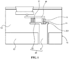
FIG. 1 illustrates a schematic structural diagram of a semiconductor structure according to an exemplary embodiment the disclosure. -
FIG. 2 illustrates a schematic structural diagram of a semiconductor structure after expansion according to an exemplary embodiment of the disclosure. -
FIG. 3 illustrates a schematic structural diagram of a conductive portion of a semiconductor structure according to an exemplary embodiment of the disclosure. -
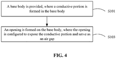
FIG. 4 illustrates a flowchart of a method for manufacturing a semiconductor structure according to an exemplary embodiment of the disclosure. -
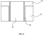
FIG. 5 illustrates a schematic structural diagram of a process for forming a via portion according to the method for manufacturing the semiconductor structure shown in an exemplary embodiment of the disclosure. -
FIG. 6 illustrates a schematic structural diagram of a process for forming a first insulating layer according to the method for manufacturing the semiconductor structure shown in an exemplary embodiment of the disclosure. -
FIG. 7 illustrates a schematic structural diagram of a process for forming a groove according to the method for manufacturing the semiconductor structure shown in an exemplary embodiment of the disclosure. -
FIG. 8 illustrates a schematic structural diagram of a process for forming a first conductive layer according to the method for manufacturing the semiconductor structure shown in an exemplary embodiment of the disclosure. -
FIG. 9 illustrates a schematic structural diagram of a process for forming a second insulating layer according to the method for manufacturing the semiconductor structure shown in an exemplary embodiment of the disclosure. -
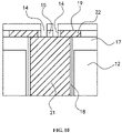
FIG. 10 illustrates a schematic structural diagram of a process for forming an opening according to the method for manufacturing the semiconductor structure shown in an exemplary embodiment of the disclosure. -
FIG. 11 illustrates a schematic structural diagram of a process for forming an insulating covering layer according to the method for manufacturing the semiconductor structure shown in an exemplary embodiment of the disclosure. -
FIG. 12 illustrates a schematic structural diagram of a process for thinning the insulating covering layer according to the method for manufacturing the semiconductor structure shown in an exemplary embodiment of the disclosure. - The reference numerals are explained as follows:
- 10: base; 11: air gap; 12: silicon substrate; 13: insulating layer; 20: conductive portion; 21: via portion; 22: first conductive layer; 221: via; 30: second conductive layer; 31: connecting column;
- 14: opening; 15: first insulating layer; 16: groove; 17: bottom insulating layer; 18: sidewall insulating layer; 19: second insulating layer; 151: insulating covering layer.
- Typical embodiments embodying the features and advantages of the disclosure will be described in detail in the following description. It should be understood that the disclosure can have various changes in different embodiments, which do not depart from the scope of the disclosure, and the description and figures therein are essentially for illustrative purposes, rather than limiting the disclosure.
- In the following description of different exemplary embodiments of the disclosure, reference may be made to the figures, which form a part of the disclosure. And different exemplary structures, systems, and steps that can implement various aspects of the disclosure may be shown by the way of example. It should be understood that other specific solutions of components, structures, exemplary devices, systems, and steps can be used, and structural and functional modifications can be made without departing from the scope of the disclosure. Moreover, although the terms of "above", "between", "within", etc. may be used in the specification to describe different exemplary features and elements of the disclosure, these terms are used herein for convenience only, for example, according to the directions of the examples in the figures. Nothing in the specification should be understood as requiring a specific three-dimensional direction of the structure to fall within the scope of the disclosure.
- An embodiment of the disclosure provides a semiconductor structure. Referring to
FIG. 1 , the semiconductor structure includes abase 10 and aconductive portion 20 arranged in thebase 10, where theconductive portion 20 includes avia portion 21 and a firstconductive layer 22. The firstconductive layer 22 is connected with thevia portion 21 and arranged above thevia portion 21. Anair gap 11 is arranged in thebase 10, and one end of the air gap is configured to expose theconductive portion 20. - The semiconductor structure of the disclosure includes the
base 10 and theconductive portion 20 that includes thevia portion 21 and the firstconductive layer 22. By arranging theair gap 11 in thebase 10 and exposing theair gap 11 to theconductive portion 20 in thebase 10, a part of the conductive material of theconductive portion 20 may enter theair gap 11 during the thermal expansion of the conductive material in thevia portion 21, so as to avoid squeezing the surrounding lattice of thevia portion 21. - Specifically, as shown in
FIG. 1 , in a normal state of theconductive portion 20, there may be no conductive material of theconductive portion 20 in theair gap 11, but when the conductive material of thevia portion 21 and the conductive material of the firstconductive layer 22 may be thermally expanded. As shown inFIG. 2 , part of the conductive material will enter theair gap 11, so as to prevent theconductive portion 20 from squeezing the surrounding lattice of thevia portion 21 or other adjacent conductive layers after the thermal expansion. - In an embodiment, the
via portion 21 may include copper (Cu), tungsten (W) and other conductive materials related to an integrated circuit. Thevia portion 21 may be interpreted as a via formed in thebase 10 where the conductive material is filled in the via. In the embodiment, the via may be filled with copper. - In some embodiments, the
via portion 21 may be a silicon via. - In an embodiment, one end of the
air gap 11 may be configured to expose a top end of thevia portion 21. That is, after thevia portion 21 being thermally expanded, the conductive material of thevia portion 21 may directly enter theair gap 11, thereby prevent the conductive material from squeezing the surrounding lattice of thevia portion 21 or other adjacent conductive layers. - It should be noted that the
air gap 11 may include a first end and a second end. Both of the first end and the second end of theair gap 11 may be arranged in thebase 10, a cavity may be formed in theair gap 11, and the top end of thevia 21 may be directly connected with the first end or the second end of theair gap 11. Therefore, after thevia portion 21 being thermally expanded, part of the conductive material of thevia portion 21 can directly enter theair gap 11, thereby prevent conductive material from squeezing the surrounding lattice of thevia portion 21 or other adjacent conductive layers. - In an embodiment, as shown in
FIGS. 1 and3 , avia 221 may be arranged on the firstconductive layer 22, to expose the top end of thevia portion 21, and at least part of theair gap 11 may be arranged in thevia 221. - Specifically, the
via 221 may be formed inside of the firstconductive layer 22, and part of thevia 221 may be filled, and the other unfilled space may form at least part of theair gap 11. This arrangement can allow one end of theair gap 11 to expose the top end of thevia 21, so as to ensure that part of the conductive materials of thevia portion 21 can directly enter theair gap 11 after thevia 21 being thermally expanded. Moreover, the filled part in thevia 221 may not be the conductive material, so the arrangement of thevia 221 can protect the firstconductive layer 22 and also prevent other problems caused by the deformation (e.g., a fracture) of the firstconductive layer 22. Due to the existence of the via 221, the thermal expansion of the firstconductive layer 22 will also be released, so as to further protect the firstconductive layer 22. - In some embodiments, a height of the
air gap 11 may be equal to a height of the via 221; that is, the height of theair gap 11 may be equal to a thickness of the firstconductive layer 22. - In some embodiments, the height of the
air gap 11 may be greater than the height of the via 221; that is, the height of theair gap 11 may be greater than the thickness of the firstconductive layer 22, so that the height of theair gap 11 will be high enough to form sufficient reserved space, to ensure that the conductive material of the viaportion 21 can have sufficient expansion space after the thermal expansion of the viaportion 21. - In some embodiments, the via 221 may be an edge cut, that is, it can be understood as a cutting part of the material at the edge of the first
conductive layer 22, thereby forming an opening that can expose the top end of the viaportion 21. Therefore, after theair gap 11 being formed, the top end of the viaportion 21 may be exposed by theair gap 11. - In some embodiments, the via 221 may be arranged in a middle of the first
conductive layer 22; that is, the via 221 may be an internal via with a circumferentially closed sidewall formed by the firstconductive layer 22, which can be regarded as digging a via inside of the firstconductive layer 22 to expose the top end of the viaportion 21. Therefore, after theair gap 11 being formed, the top end of the viaportion 21 may be exposed by theair gap 11. - It should be noted that the middle of the first
conductive layer 22 may refer to a location other than the circumferential sidewall of the firstconductive layer 22, which means that the via 221 does not intersect the circumferential sidewall of the firstconductive layer 22. - It should be noted that the specific shape of the via 221 will not be limited, and it may be a polygonal hole, a circular hole, or a special-shaped hole, etc.
- Correspondingly, the specific shape of the
air gap 11 will not be limited, and it may be a polygonal hole, a circular hole, or a special-shaped hole, etc. - In one embodiment, an area of a cross section of the via 221 may be smaller than an area of a cross section of the via
portion 21, so as to ensure that the firstconductive layer 22 can be reliably connected with the viaportion 21, and further to ensure that there will be a space for forming theair gap 11. - In one embodiment, the height of the
air gap 11 may be greater than the thickness of the firstconductive layer 22, so as to ensure that theair gap 11 may have enough space. Therefore, after the viaportion 21 being thermally expanded, part of the conductive material of the viaportion 21 can enter into theair gap 11. - In one embodiment, as shown in
FIG. 1 , the semiconductor structure may further include a secondconductive layer 30 which is arranged in thebase 10. The secondconductive layer 30 may be spaced apart from the firstconductive layer 22, and arranged above the firstconductive layer 22. Theair gap 11 may be arranged under the secondconductive layer 30 and spaced apart from the secondconductive layer 30. Therefore, after the conductive material entering theair gap 11, the secondconductive layer 30 may not be connected with the conductive material in theair gap 11. - As shown in
FIGS. 1 and2 , the firstconductive layer 22 may be connected with the secondconductive layer 30 through a connecting column 31 ( i.e., a conductive structure), and theair gap 11 may be directly arranged under the secondconductive layer 30. In this case, it will be necessary to ensure that theair gap 11 can be spaced apart from the secondconductive layer 30; that is, the top end of theair gap 11 may not expose the secondconductive layer 30. - In one embodiment, the first
conductive layer 22 may include a plurality of sub-conductive layers that are spaced apart from each other, and two adjacent sub-conductive layers from the plurality of sub-conductive layers may be configured to expose the top end of the viaportion 21. At least part of theair gap 11 may be arranged between the two adjacent sub-conductive layers. - Compared with the via 221 arranged on the first
conductive layer 22, this structure may form an exposed space through the plurality of sub-conductive layers that are spaced apart from each other. Therefore, theair gap 11 can be formed between two adjacent sub-conductive layers. For example, a plurality of sub-conductive layers parallel to each other can be provided, and at least part of the plurality of sub-conductive layers may be connected with the viaportion 21. The plurality of sub-conductive layers may be all electrically connected. For example, the conductive layer may be arranged on the plurality of sub-conductive layers for electrical connection, or it may be connected with the secondconductive layer 30 through the connectingcolumn 31. That is, the electrical connection of the plurality of sub-conductive layers can also be realized. The electrical connection manner of the plurality of sub-conductive layers will not be limited here. - In one embodiment, one end of the
air gap 11 may be configured to expose the top end of the firstconductive layer 22, where theair gap 11 may be arranged directly above the viaportion 21. In this way, even if one end of theair gap 11 is not directly connected with the viaportion 21, since the viaportion 21 and theair gap 11 are directly opposed to each other, even if viaportion 21 is thermally expanded to squeeze the firstconductive layer 22 between the viaportion 21 and theair gap 11, the conductive material can be allowed to enter theair gap 11, thereby preventing the conductive material from squeezing the surrounding lattice of the viaportion 21 or other adjacent conductive layers. - In one embodiment, the
air gap 11 may include a plurality of air gap arranged at an interval, and each of the plurality of air gaps may be configured to expose the conductive portion, so that the conductive material can have sufficient expansion space. - In one embodiment, as shown in
FIGS. 1 and2 , thebase 10 may include asilicon substrate 12, where a top end of thesilicon substrate 12 may be higher than an upper surface of thesilicon substrate 12. And the base 10 may further include an insulatinglayer 13, which may be configured to cover the upper surface of thesilicon substrate 12 and cover an outer surface of the viaportion 21. Both of the firstconductive layer 22 and theair gap 11 may be arranged in the insulatinglayer 13. - Specifically, the
silicon substrate 12 may be formed of a silicon-containing material. Thesilicon substrate 12 may be formed of any suitable material, for example, including at least one of silicon, single crystal silicon, amorphous silicon, silicon germanium, single crystal silicon germanium, silicon carbide, and sapphire. - The insulating
layer 13 may include silicon dioxide (SiO2), silicon oxycarbide (SiOC), silicon nitride (SiN), silicon carbonitride (SiCN) and other insulating materials related to the integrated circuit. The insulatinglayer 13 may fill part of thevia 221. - It should be noted that the
silicon substrate 12 and the insulatinglayer 13 may also be provided with other conductive structures, which will not be limited herein, and can be selected according to the requirements in the related art. - The semiconductor structure of the disclosure may relate to a wafer process technology, in particular to a via portion manufacturing technology. In most of the via portion manufacturing technologies, copper metal will be filled in the via portion as the conductive material. However, excessive thermal expansion of copper will affect the surrounding lattice of the via portion or the deformation of the upper metal layer, which can lead to a reduction of the yield or the reliability of the chip in serious cases. Therefore, in related art, the upper metal layer usually does not arrange effective circuits, which wastes the chip design space and also affects the size of the chip. The semiconductor structure of the disclosure uses the air gap to prevent metal protrusions during copper thermal expansion, that is, the
air gap 11 can be used as a buffer space during copper expansion to reduce the impact of metal thermal expansion on the upper circuit. In this way, the upper space of the via portion can be used for circuit design, and thus, the size of the chip design can be reduced. - In some embodiments, the via 221 may be a circular hole, the diameter of the via 221 may be between 1 µm and 10 µm, and the diameter of the via 221 may not be greater than the diameter of the via
portion 21. In some embodiments, the diameter of the via 221 may be equal to half of the diameter of the viaportion 21. - In some embodiments, the
air gap 11 may be a circular hole, the diameter of theair gap 11 may be between 20 nm and 200 nm, and the height may be between 50 nm and 200 nm, and there may be one ormore air gaps 11. - An embodiment of the disclosure further provides a method for manufacturing a semiconductor structure. Referring to
FIG. 4 , the method for manufacturing the semiconductor structure includes the following operations of S101 and S103. - In the operation of S101, a base body is set, where a
conductive portion 20 is formed in the base body, and theconductive portion 20 includes a viaportion 21 and a firstconductive layer 22. The firstconductive layer 22 may be connected with the viaportion 21 and arranged above the viaportion 21. - In the operation of S103, an
opening 14 is formed on the base body, where the opening is configured to expose theconductive portion 20 and serve as anair gap 11. - In the method for manufacturing the semiconductor structure according to one embodiment of the disclosure, by forming the
air gap 11 in the base body, theair gap 11 may be configured to expose theconductive portion 20 arranged in the base body. Therefore, part of the conductive material of theconductive portion 20 can enter theair gap 11 during the thermal expansion of the conductive material of the viaportion 21, so as to avoid squeezing the surrounding lattice of the viaportion 21. - In some embodiments, as shown in
FIG. 5 , the base body may include asilicon substrate 12, a bottom insulatinglayer 17, and asidewall insulating layer 18. The bottom insulatinglayer 17 may be formed on the upper surface of thesilicon substrate 12 and the inside of thesilicon substrate 12. And thesidewall insulating layer 18 may be formed inside of thebottom insulation layer 17 and may cover the sidewall of the viaportion 21. - It should be noted that the bottom insulating
layer 17 and thesidewall insulating layer 18 may include silicon dioxide (SiO2), silicon oxycarbide (SiOC), silicon nitride (SiN), silicon carbonitride (SiCN) and other insulating materials related to the integrated circuit. - The bottom insulating
layer 17 and thesidewall insulating layer 18 may be insulating materials of the same material or insulating materials of different materials. - It should be noted that the forming process of the bottom insulating
layer 17, thesidewall insulating layer 18, and the viaportion 21 can be selected from a Physical Vapor Deposition (PVD) process, a Chemical Vapor Deposition (CVD) process, an Atomic Layer Deposition (ALD) process, an In-Situ Steam Generation (ISSG) process, and a Spin On Dielectric (SOD) process, etc., which will not be limited herein. - In one embodiment, the method for manufacturing the semiconductor structure may further include an operation of forming an insulating
covering layer 151 that may be configured to cover a top end of theopening 14 on the base body, so that theair gap 11 may be formed in the base body. - In one embodiment, the
opening 14 may be configured to expose the top end of the viaportion 21; that is, after the viaportion 21 being thermally expanded, the conductive material of the viaportion 21 can directly enter theair gap 11, thereby preventing the conductive material from squeezing the surrounding lattice of the viaportion 21 or other adjacent conductive layers. - In one embodiment, as shown in
FIG. 6 , a first insulatinglayer 15 may be formed on the bottom insulatinglayer 17, and the first insulatinglayer 15 may be configured to cover the top end of the viaportion 21. - In one embodiment, the operation of forming the
opening 14 may include: forming agroove 16 on the first insulatinglayer 15, to expose part of the top end of the viaportion 21; forming the firstconductive layer 22 in thegroove 16; forming a second insulatinglayer 19 that may be configured to cover the firstconductive layer 22 on the first insulatinglayer 15; and forming theopening 14 on the second insulatinglayer 19 and the first insulatinglayer 15. - Specifically, the remaining part of the first insulating
layer 15 may be surrounded by thegroove 16, and the space occupied by the remaining part of the first insulatinglayer 15 may be the via 221 in the firstconductive layer 22. - As shown in
FIG. 7 , on the basis ofFIG. 6 , thegroove 16 may be formed in the first insulatinglayer 15, and thegroove 16 may be an annular via, thereby exposing a part of the top end of the viaportion 21. - On the basis of
FIG. 7 , the conductive material may be filled in thegroove 16 to form the firstconductive layer 22 as shown inFIG. 8 . At the time, the firstconductive layer 22 may be connected with the viaportion 21. The firstconductive layer 22 may be provided with the first insulatinglayer 15 inside. - On the basis of
FIG. 8 , as shown inFIG. 9 in detail, the second insulatinglayer 19 may be covered on the first insulatinglayer 15 and the firstconductive layer 22. - On the basis of
FIG. 9 , as shown inFIG. 10 , theopening 14 may be formed in the second insulatinglayer 19 and the first insulatinglayer 15, and theopening 14 may also expose the top end of the viaportion 21. - On the basis of
FIG. 10 , as shown inFIG. 11 , acover insulating layer 151 with a larger thickness may be formed on the second insulatinglayer 19, and then the insulatingcovering layer 151 may be thinned to form a structure as shown inFIG. 12 . - It should be noted that the first insulating
layer 15, the second insulatinglayer 19, and the insulatingcovering layer 151 may include silicon dioxide (SiO2), silicon oxycarbide (SiOC), silicon nitride (SiN), silicon carbonitride (SiCN) and other insulating materials related to the integrated circuit. - It should be noted that the forming process of the first insulating
layer 15, the second insulatinglayer 19, and the insulatingcovering layer 151 can be selected from the Physical Vapor Deposition (PVD) process, the Chemical Vapor Deposition (CVD) process, the Atomic Layer Deposition (ALD) process, the In-Situ Steam Generation (ISSG) process, and the Spin On Dielectric (SOD) process, etc., which will not be limited herein. - The forming process of the
opening 14 and thegroove 16 may include a process of photolithography, a process of etching, etc. After each coating being formed, it can be treated in combination with a Chemical Mechanical Polishing (CMP) process to ensure the flatness of the coating. The firstconductive layer 22 may be formed by a process of electroplating or sputtering, which will not be limited herein. - In one embodiment, the semiconductor structure may be formed by the aforementioned method for manufacturing the semiconductor structure. The method for manufacturing the semiconductor structure may further include the operation of forming the second
conductive layer 30, etc., which will not be limited this time. Thesilicon substrate 12 and the aforementioned insulating layers may be all parts of thebase 10. The bottom insulatinglayer 17, thesidewall insulating layer 18, the first insulatinglayer 15, the second insulatinglayer 19 and the insulatingcovering layer 151 may be all parts of the insulatinglayer 13. - After considering the specification and practicing the invention disclosed herein, those skilled in the art would easily conceive of other embodiments of the disclosure. The disclosure aims to cover various variation, usages or adaptive changes of the present invention, which follow the general principles of this disclosure and includes the common technical knowledge or commonly used technical means in the technical field not disclosed in this disclosure. The specification and exemplary embodiments are only considered exemplary, and the actual scope and spirit of the disclosure are pointed out by the preceding claims.
- It should be understood that this disclosure is not limited to the precise structure that has been described above and shown in the figures, and various modifications and changes can be made without departing from the scope. The scope of this disclosure is only limited by the appended claims.
Claims (20)
- A semiconductor structure, comprising:a base; anda conductive portion, arranged in the base, and comprising a via portion and a first conductive layer, where the first conductive layer is connected with the via portion and arranged above the via portion;wherein an air gap is arranged in the base, and one end of the air gap is configured to expose the conductive portion.
- The semiconductor structure of claim 1, wherein one end of the air gap is configured to expose a top end of the via portion.
- The semiconductor structure of claim 2, wherein a via is arranged on the first conductive layer, to expose the top end of the via portion, and at least part of the air gap is arranged in the via.
- The semiconductor structure of claim 3, wherein the via is arranged in a middle of the first conductive layer.
- The semiconductor structure of claim 3, wherein an area of a cross section of the via is smaller than an area of a cross section of the via portion.
- The semiconductor structure of claim 3, wherein a height of the air gap is greater than a thickness of the first conductive layer.
- The semiconductor structure of claim 3, wherein a height of the air gap is equal to a height of the via.
- The semiconductor structure of claim 3, wherein a height of the air gap is greater than a height of the via.
- The semiconductor structure of claim 3, wherein the air gap is a circular hole, a diameter of the air gap is between 20 nm and 200 nm, and a height of the air gap is between 50 nm and 200 nm.
- The semiconductor structure of claim 3, wherein the via is a circular hole, and a diameter of the via is between 1 µm and 10 µm.
- The semiconductor structure of claim 1 or 6, wherein the semiconductor structure further comprises:a second conductive layer, arranged in the base, wherein the second conductive layer is spaced apart from the first conductive layer, and arranged above the first conductive layer;wherein the air gap is arranged under the second conductive layer and spaced apart from the second conductive layer.
- The semiconductor structure of claim 2, wherein the first conductive layer comprises a plurality of sub-conductive layers that are spaced apart from each other, and two adjacent sub-conductive layers from the plurality of the sub-conductive layers are configured to expose the top end of the via portion; and
wherein, at least part of the air gap is arranged between the two adjacent sub-conductive layers. - The semiconductor structure of claim 1, wherein one end of the air gap is configured to expose a top end of the first conductive layer; and
wherein the air gap is arranged directly above the via portion. - The semiconductor structure of claim 1, wherein the air gap comprises a plurality of air gaps arranged at an interval, and each of the plurality of air gaps is configured to expose the conductive portion.
- The semiconductor structure according to claim 1, wherein the base comprising:a silicon substrate, wherein a top end of the silicon substrate is higher than an upper surface of the silicon substrate; andan insulating layer, configured to cover the upper surface of the silicon substrate and cover an outer surface of the via portion;wherein both of the first conductive layer and the air gap are arranged in the insulating layer.
- The semiconductor structure of claim 1, wherein the via portion is a silicon via.
- A method for manufacturing a semiconductor structure, comprising:providing a base body, wherein a conductive portion is formed in the base body, and the conductive portion comprises a via portion and a first conductive layer, wherein the first conductive layer is connected with the via portion and arranged above the via portion; andforming an opening on the base body, wherein the opening is configured to expose the conductive portion and serve as an air gap.
- The method for manufacturing the semiconductor structure of claim 17, further comprising:
forming an insulating covering layer, wherein the insulating covering layer is configured to cover a top end of the opening on the base body. - The method for manufacturing the semiconductor structure of claim 17 or 18, wherein the opening is configured to expose a top end of the via portion.
- The method for manufacturing the semiconductor structure of claim 19, wherein the base body comprises a silicon substrate and a first insulating layer, and wherein forming the opening comprises:forming a groove on the first insulating layer, to expose part of the top end of the via portion;forming the first conductive layer in the groove;forming a second insulating layer, wherein the second insulating layer is configured to cover the first conductive layer on the first insulating layer; andforming the opening on the second insulating layer and the first insulating layer.
Applications Claiming Priority (2)
| Application Number | Priority Date | Filing Date | Title |
|---|---|---|---|
| CN202110259350.XA CN115083999A (en) | 2021-03-10 | 2021-03-10 | Semiconductor structure and manufacturing method thereof |
| PCT/CN2021/110605 WO2022188346A1 (en) | 2021-03-10 | 2021-08-04 | Semiconductor structure and method for manufacturing semiconductor structure |
Publications (3)
| Publication Number | Publication Date |
|---|---|
| EP4084053A1 true EP4084053A1 (en) | 2022-11-02 |
| EP4084053A4 EP4084053A4 (en) | 2022-12-14 |
| EP4084053B1 EP4084053B1 (en) | 2024-01-31 |
Family
ID=83194001
Family Applications (1)
| Application Number | Title | Priority Date | Filing Date |
|---|---|---|---|
| EP21863069.7A Active EP4084053B1 (en) | 2021-03-10 | 2021-08-04 | Semiconductor structure and its method for manufacturing |
Country Status (2)
| Country | Link |
|---|---|
| US (1) | US20220293456A1 (en) |
| EP (1) | EP4084053B1 (en) |
Family Cites Families (4)
| Publication number | Priority date | Publication date | Assignee | Title |
|---|---|---|---|---|
| US7855438B2 (en) * | 2006-09-19 | 2010-12-21 | Infineon Technologies Ag | Deep via construction for a semiconductor device |
| KR101959284B1 (en) * | 2011-11-18 | 2019-03-19 | 삼성전자주식회사 | Semiconductor device and method of forming the same |
| US10847442B2 (en) * | 2014-02-24 | 2020-11-24 | Micron Technology, Inc. | Interconnect assemblies with through-silicon vias and stress-relief features |
| JP6805633B2 (en) * | 2016-08-24 | 2020-12-23 | 富士通株式会社 | Electronic devices and their manufacturing methods |
-
2021
- 2021-08-04 EP EP21863069.7A patent/EP4084053B1/en active Active
-
2022
- 2022-02-10 US US17/668,644 patent/US20220293456A1/en not_active Abandoned
Also Published As
| Publication number | Publication date |
|---|---|
| EP4084053B1 (en) | 2024-01-31 |
| US20220293456A1 (en) | 2022-09-15 |
| EP4084053A4 (en) | 2022-12-14 |
Similar Documents
| Publication | Publication Date | Title |
|---|---|---|
| US8183685B2 (en) | Semiconductor device | |
| US7772123B2 (en) | Through substrate via semiconductor components | |
| US8415806B2 (en) | Semiconductor structure and method for manufacturing the same | |
| CN110648976B (en) | Semiconductor devices and methods of manufacturing same | |
| KR101959284B1 (en) | Semiconductor device and method of forming the same | |
| US20170352592A1 (en) | Integrated circuit structure having deep trench capacitor and through-silicon via and method of forming same | |
| US6077767A (en) | Modified implementation of air-gap low-K dielectric for unlanded via | |
| US9834436B2 (en) | Cap and substrate electrical connection at wafer level | |
| KR20230145955A (en) | Backside or frontside through substrate via (tsv) landing on metal | |
| US20170352618A1 (en) | Integrated circuit structure having deep trench capacitor and through-silicon via and method of forming same | |
| US8765590B2 (en) | Insulative cap for borderless self-aligning contact in semiconductor device | |
| CN113078140B (en) | Manufacturing method of semiconductor structure and semiconductor structure | |
| US10770395B2 (en) | Silicon carbide and silicon nitride interconnects | |
| US9831122B2 (en) | Integrated circuit including wire structure, related method and design structure | |
| EP4084053B1 (en) | Semiconductor structure and its method for manufacturing | |
| CN103378028B (en) | Semiconductor structure with stress protection structure and method of forming same | |
| CN115083999A (en) | Semiconductor structure and manufacturing method thereof | |
| JP7387003B2 (en) | Semiconductor structure and method for manufacturing semiconductor structure | |
| US12100670B2 (en) | Method for manufacturing semiconductor structure and semiconductor structure | |
| US12593677B2 (en) | Semiconductor device structure with energy removable structure and method for preparing the same | |
| US6864582B1 (en) | Semiconductor interconnect and method of providing interconnect using a contact region | |
| EP4117030A1 (en) | Semiconductor structure and method for manufacturing same | |
| TW202527246A (en) | Semiconductor structure and method of manufacturing the same | |
| WO2022188358A1 (en) | Semiconductor structure and manufacturing method for same |
Legal Events
| Date | Code | Title | Description |
|---|---|---|---|
| STAA | Information on the status of an ep patent application or granted ep patent |
Free format text: STATUS: UNKNOWN |
|
| STAA | Information on the status of an ep patent application or granted ep patent |
Free format text: STATUS: THE INTERNATIONAL PUBLICATION HAS BEEN MADE |
|
| PUAI | Public reference made under article 153(3) epc to a published international application that has entered the european phase |
Free format text: ORIGINAL CODE: 0009012 |
|
| STAA | Information on the status of an ep patent application or granted ep patent |
Free format text: STATUS: REQUEST FOR EXAMINATION WAS MADE |
|
| 17P | Request for examination filed |
Effective date: 20220309 |
|
| AK | Designated contracting states |
Kind code of ref document: A1 Designated state(s): AL AT BE BG CH CY CZ DE DK EE ES FI FR GB GR HR HU IE IS IT LI LT LU LV MC MK MT NL NO PL PT RO RS SE SI SK SM TR |
|
| A4 | Supplementary search report drawn up and despatched |
Effective date: 20221116 |
|
| RIC1 | Information provided on ipc code assigned before grant |
Ipc: H01L 23/48 20060101ALI20221110BHEP Ipc: H01L 23/522 20060101ALI20221110BHEP Ipc: H01L 21/768 20060101AFI20221110BHEP |
|
| STAA | Information on the status of an ep patent application or granted ep patent |
Free format text: STATUS: EXAMINATION IS IN PROGRESS |
|
| 17Q | First examination report despatched |
Effective date: 20230302 |
|
| GRAP | Despatch of communication of intention to grant a patent |
Free format text: ORIGINAL CODE: EPIDOSNIGR1 |
|
| STAA | Information on the status of an ep patent application or granted ep patent |
Free format text: STATUS: GRANT OF PATENT IS INTENDED |
|
| DAV | Request for validation of the european patent (deleted) | ||
| DAX | Request for extension of the european patent (deleted) | ||
| INTG | Intention to grant announced |
Effective date: 20230823 |
|
| P01 | Opt-out of the competence of the unified patent court (upc) registered |
Effective date: 20230916 |
|
| GRAS | Grant fee paid |
Free format text: ORIGINAL CODE: EPIDOSNIGR3 |
|
| GRAA | (expected) grant |
Free format text: ORIGINAL CODE: 0009210 |
|
| STAA | Information on the status of an ep patent application or granted ep patent |
Free format text: STATUS: THE PATENT HAS BEEN GRANTED |
|
| AK | Designated contracting states |
Kind code of ref document: B1 Designated state(s): AL AT BE BG CH CY CZ DE DK EE ES FI FR GB GR HR HU IE IS IT LI LT LU LV MC MK MT NL NO PL PT RO RS SE SI SK SM TR |
|
| REG | Reference to a national code |
Ref country code: GB Ref legal event code: FG4D Ref country code: CH Ref legal event code: EP |
|
| REG | Reference to a national code |
Ref country code: DE Ref legal event code: R096 Ref document number: 602021009109 Country of ref document: DE |
|
| REG | Reference to a national code |
Ref country code: IE Ref legal event code: FG4D |
|
| REG | Reference to a national code |
Ref country code: LT Ref legal event code: MG9D |
|
| REG | Reference to a national code |
Ref country code: NL Ref legal event code: MP Effective date: 20240131 |
|
| PG25 | Lapsed in a contracting state [announced via postgrant information from national office to epo] |
Ref country code: IS Free format text: LAPSE BECAUSE OF FAILURE TO SUBMIT A TRANSLATION OF THE DESCRIPTION OR TO PAY THE FEE WITHIN THE PRESCRIBED TIME-LIMIT Effective date: 20240531 |
|
| PG25 | Lapsed in a contracting state [announced via postgrant information from national office to epo] |
Ref country code: LT Free format text: LAPSE BECAUSE OF FAILURE TO SUBMIT A TRANSLATION OF THE DESCRIPTION OR TO PAY THE FEE WITHIN THE PRESCRIBED TIME-LIMIT Effective date: 20240131 |
|
| PG25 | Lapsed in a contracting state [announced via postgrant information from national office to epo] |
Ref country code: GR Free format text: LAPSE BECAUSE OF FAILURE TO SUBMIT A TRANSLATION OF THE DESCRIPTION OR TO PAY THE FEE WITHIN THE PRESCRIBED TIME-LIMIT Effective date: 20240501 |
|
| REG | Reference to a national code |
Ref country code: AT Ref legal event code: MK05 Ref document number: 1654455 Country of ref document: AT Kind code of ref document: T Effective date: 20240131 |
|
| PG25 | Lapsed in a contracting state [announced via postgrant information from national office to epo] |
Ref country code: HR Free format text: LAPSE BECAUSE OF FAILURE TO SUBMIT A TRANSLATION OF THE DESCRIPTION OR TO PAY THE FEE WITHIN THE PRESCRIBED TIME-LIMIT Effective date: 20240131 Ref country code: RS Free format text: LAPSE BECAUSE OF FAILURE TO SUBMIT A TRANSLATION OF THE DESCRIPTION OR TO PAY THE FEE WITHIN THE PRESCRIBED TIME-LIMIT Effective date: 20240430 Ref country code: NL Free format text: LAPSE BECAUSE OF FAILURE TO SUBMIT A TRANSLATION OF THE DESCRIPTION OR TO PAY THE FEE WITHIN THE PRESCRIBED TIME-LIMIT Effective date: 20240131 |
|
| PG25 | Lapsed in a contracting state [announced via postgrant information from national office to epo] |
Ref country code: ES Free format text: LAPSE BECAUSE OF FAILURE TO SUBMIT A TRANSLATION OF THE DESCRIPTION OR TO PAY THE FEE WITHIN THE PRESCRIBED TIME-LIMIT Effective date: 20240131 |
|
| PG25 | Lapsed in a contracting state [announced via postgrant information from national office to epo] |
Ref country code: AT Free format text: LAPSE BECAUSE OF FAILURE TO SUBMIT A TRANSLATION OF THE DESCRIPTION OR TO PAY THE FEE WITHIN THE PRESCRIBED TIME-LIMIT Effective date: 20240131 |
|
| PG25 | Lapsed in a contracting state [announced via postgrant information from national office to epo] |
Ref country code: RS Free format text: LAPSE BECAUSE OF FAILURE TO SUBMIT A TRANSLATION OF THE DESCRIPTION OR TO PAY THE FEE WITHIN THE PRESCRIBED TIME-LIMIT Effective date: 20240430 Ref country code: NO Free format text: LAPSE BECAUSE OF FAILURE TO SUBMIT A TRANSLATION OF THE DESCRIPTION OR TO PAY THE FEE WITHIN THE PRESCRIBED TIME-LIMIT Effective date: 20240430 Ref country code: NL Free format text: LAPSE BECAUSE OF FAILURE TO SUBMIT A TRANSLATION OF THE DESCRIPTION OR TO PAY THE FEE WITHIN THE PRESCRIBED TIME-LIMIT Effective date: 20240131 Ref country code: LT Free format text: LAPSE BECAUSE OF FAILURE TO SUBMIT A TRANSLATION OF THE DESCRIPTION OR TO PAY THE FEE WITHIN THE PRESCRIBED TIME-LIMIT Effective date: 20240131 Ref country code: IS Free format text: LAPSE BECAUSE OF FAILURE TO SUBMIT A TRANSLATION OF THE DESCRIPTION OR TO PAY THE FEE WITHIN THE PRESCRIBED TIME-LIMIT Effective date: 20240531 Ref country code: HR Free format text: LAPSE BECAUSE OF FAILURE TO SUBMIT A TRANSLATION OF THE DESCRIPTION OR TO PAY THE FEE WITHIN THE PRESCRIBED TIME-LIMIT Effective date: 20240131 Ref country code: GR Free format text: LAPSE BECAUSE OF FAILURE TO SUBMIT A TRANSLATION OF THE DESCRIPTION OR TO PAY THE FEE WITHIN THE PRESCRIBED TIME-LIMIT Effective date: 20240501 Ref country code: FI Free format text: LAPSE BECAUSE OF FAILURE TO SUBMIT A TRANSLATION OF THE DESCRIPTION OR TO PAY THE FEE WITHIN THE PRESCRIBED TIME-LIMIT Effective date: 20240131 Ref country code: ES Free format text: LAPSE BECAUSE OF FAILURE TO SUBMIT A TRANSLATION OF THE DESCRIPTION OR TO PAY THE FEE WITHIN THE PRESCRIBED TIME-LIMIT Effective date: 20240131 Ref country code: BG Free format text: LAPSE BECAUSE OF FAILURE TO SUBMIT A TRANSLATION OF THE DESCRIPTION OR TO PAY THE FEE WITHIN THE PRESCRIBED TIME-LIMIT Effective date: 20240131 Ref country code: AT Free format text: LAPSE BECAUSE OF FAILURE TO SUBMIT A TRANSLATION OF THE DESCRIPTION OR TO PAY THE FEE WITHIN THE PRESCRIBED TIME-LIMIT Effective date: 20240131 |
|
| PG25 | Lapsed in a contracting state [announced via postgrant information from national office to epo] |
Ref country code: PL Free format text: LAPSE BECAUSE OF FAILURE TO SUBMIT A TRANSLATION OF THE DESCRIPTION OR TO PAY THE FEE WITHIN THE PRESCRIBED TIME-LIMIT Effective date: 20240131 Ref country code: PT Free format text: LAPSE BECAUSE OF FAILURE TO SUBMIT A TRANSLATION OF THE DESCRIPTION OR TO PAY THE FEE WITHIN THE PRESCRIBED TIME-LIMIT Effective date: 20240531 |
|
| PG25 | Lapsed in a contracting state [announced via postgrant information from national office to epo] |
Ref country code: SE Free format text: LAPSE BECAUSE OF FAILURE TO SUBMIT A TRANSLATION OF THE DESCRIPTION OR TO PAY THE FEE WITHIN THE PRESCRIBED TIME-LIMIT Effective date: 20240131 Ref country code: PT Free format text: LAPSE BECAUSE OF FAILURE TO SUBMIT A TRANSLATION OF THE DESCRIPTION OR TO PAY THE FEE WITHIN THE PRESCRIBED TIME-LIMIT Effective date: 20240531 Ref country code: PL Free format text: LAPSE BECAUSE OF FAILURE TO SUBMIT A TRANSLATION OF THE DESCRIPTION OR TO PAY THE FEE WITHIN THE PRESCRIBED TIME-LIMIT Effective date: 20240131 Ref country code: LV Free format text: LAPSE BECAUSE OF FAILURE TO SUBMIT A TRANSLATION OF THE DESCRIPTION OR TO PAY THE FEE WITHIN THE PRESCRIBED TIME-LIMIT Effective date: 20240131 |
|
| PG25 | Lapsed in a contracting state [announced via postgrant information from national office to epo] |
Ref country code: DK Free format text: LAPSE BECAUSE OF FAILURE TO SUBMIT A TRANSLATION OF THE DESCRIPTION OR TO PAY THE FEE WITHIN THE PRESCRIBED TIME-LIMIT Effective date: 20240131 |
|
| PG25 | Lapsed in a contracting state [announced via postgrant information from national office to epo] |
Ref country code: SM Free format text: LAPSE BECAUSE OF FAILURE TO SUBMIT A TRANSLATION OF THE DESCRIPTION OR TO PAY THE FEE WITHIN THE PRESCRIBED TIME-LIMIT Effective date: 20240131 |
|
| PG25 | Lapsed in a contracting state [announced via postgrant information from national office to epo] |
Ref country code: EE Free format text: LAPSE BECAUSE OF FAILURE TO SUBMIT A TRANSLATION OF THE DESCRIPTION OR TO PAY THE FEE WITHIN THE PRESCRIBED TIME-LIMIT Effective date: 20240131 Ref country code: CZ Free format text: LAPSE BECAUSE OF FAILURE TO SUBMIT A TRANSLATION OF THE DESCRIPTION OR TO PAY THE FEE WITHIN THE PRESCRIBED TIME-LIMIT Effective date: 20240131 |
|
| PG25 | Lapsed in a contracting state [announced via postgrant information from national office to epo] |
Ref country code: SK Free format text: LAPSE BECAUSE OF FAILURE TO SUBMIT A TRANSLATION OF THE DESCRIPTION OR TO PAY THE FEE WITHIN THE PRESCRIBED TIME-LIMIT Effective date: 20240131 |
|
| PG25 | Lapsed in a contracting state [announced via postgrant information from national office to epo] |
Ref country code: SM Free format text: LAPSE BECAUSE OF FAILURE TO SUBMIT A TRANSLATION OF THE DESCRIPTION OR TO PAY THE FEE WITHIN THE PRESCRIBED TIME-LIMIT Effective date: 20240131 Ref country code: SK Free format text: LAPSE BECAUSE OF FAILURE TO SUBMIT A TRANSLATION OF THE DESCRIPTION OR TO PAY THE FEE WITHIN THE PRESCRIBED TIME-LIMIT Effective date: 20240131 Ref country code: RO Free format text: LAPSE BECAUSE OF FAILURE TO SUBMIT A TRANSLATION OF THE DESCRIPTION OR TO PAY THE FEE WITHIN THE PRESCRIBED TIME-LIMIT Effective date: 20240131 Ref country code: EE Free format text: LAPSE BECAUSE OF FAILURE TO SUBMIT A TRANSLATION OF THE DESCRIPTION OR TO PAY THE FEE WITHIN THE PRESCRIBED TIME-LIMIT Effective date: 20240131 Ref country code: DK Free format text: LAPSE BECAUSE OF FAILURE TO SUBMIT A TRANSLATION OF THE DESCRIPTION OR TO PAY THE FEE WITHIN THE PRESCRIBED TIME-LIMIT Effective date: 20240131 Ref country code: CZ Free format text: LAPSE BECAUSE OF FAILURE TO SUBMIT A TRANSLATION OF THE DESCRIPTION OR TO PAY THE FEE WITHIN THE PRESCRIBED TIME-LIMIT Effective date: 20240131 |
|
| REG | Reference to a national code |
Ref country code: DE Ref legal event code: R097 Ref document number: 602021009109 Country of ref document: DE |
|
| PG25 | Lapsed in a contracting state [announced via postgrant information from national office to epo] |
Ref country code: IT Free format text: LAPSE BECAUSE OF FAILURE TO SUBMIT A TRANSLATION OF THE DESCRIPTION OR TO PAY THE FEE WITHIN THE PRESCRIBED TIME-LIMIT Effective date: 20240131 |
|
| PLBE | No opposition filed within time limit |
Free format text: ORIGINAL CODE: 0009261 |
|
| STAA | Information on the status of an ep patent application or granted ep patent |
Free format text: STATUS: NO OPPOSITION FILED WITHIN TIME LIMIT |
|
| PG25 | Lapsed in a contracting state [announced via postgrant information from national office to epo] |
Ref country code: IT Free format text: LAPSE BECAUSE OF FAILURE TO SUBMIT A TRANSLATION OF THE DESCRIPTION OR TO PAY THE FEE WITHIN THE PRESCRIBED TIME-LIMIT Effective date: 20240131 |
|
| 26N | No opposition filed |
Effective date: 20241101 |
|
| REG | Reference to a national code |
Ref country code: CH Ref legal event code: PL |
|
| PG25 | Lapsed in a contracting state [announced via postgrant information from national office to epo] |
Ref country code: LU Free format text: LAPSE BECAUSE OF NON-PAYMENT OF DUE FEES Effective date: 20240804 |
|
| PG25 | Lapsed in a contracting state [announced via postgrant information from national office to epo] |
Ref country code: SI Free format text: LAPSE BECAUSE OF FAILURE TO SUBMIT A TRANSLATION OF THE DESCRIPTION OR TO PAY THE FEE WITHIN THE PRESCRIBED TIME-LIMIT Effective date: 20240131 Ref country code: MC Free format text: LAPSE BECAUSE OF FAILURE TO SUBMIT A TRANSLATION OF THE DESCRIPTION OR TO PAY THE FEE WITHIN THE PRESCRIBED TIME-LIMIT Effective date: 20240131 Ref country code: CH Free format text: LAPSE BECAUSE OF NON-PAYMENT OF DUE FEES Effective date: 20240831 |
|
| REG | Reference to a national code |
Ref country code: BE Ref legal event code: MM Effective date: 20240831 |
|
| PG25 | Lapsed in a contracting state [announced via postgrant information from national office to epo] |
Ref country code: BE Free format text: LAPSE BECAUSE OF NON-PAYMENT OF DUE FEES Effective date: 20240831 |
|
| PG25 | Lapsed in a contracting state [announced via postgrant information from national office to epo] |
Ref country code: FR Free format text: LAPSE BECAUSE OF NON-PAYMENT OF DUE FEES Effective date: 20240831 |
|
| PG25 | Lapsed in a contracting state [announced via postgrant information from national office to epo] |
Ref country code: IE Free format text: LAPSE BECAUSE OF NON-PAYMENT OF DUE FEES Effective date: 20240804 |
|
| PGFP | Annual fee paid to national office [announced via postgrant information from national office to epo] |
Ref country code: DE Payment date: 20250820 Year of fee payment: 5 |
|
| REG | Reference to a national code |
Ref country code: DE Ref legal event code: R079 Ref document number: 602021009109 Country of ref document: DE Free format text: PREVIOUS MAIN CLASS: H01L0021768000 Ipc: H10W0020000000 |
|
| PG25 | Lapsed in a contracting state [announced via postgrant information from national office to epo] |
Ref country code: CY Free format text: LAPSE BECAUSE OF FAILURE TO SUBMIT A TRANSLATION OF THE DESCRIPTION OR TO PAY THE FEE WITHIN THE PRESCRIBED TIME-LIMIT; INVALID AB INITIO Effective date: 20210804 |
|
| PG25 | Lapsed in a contracting state [announced via postgrant information from national office to epo] |
Ref country code: HU Free format text: LAPSE BECAUSE OF FAILURE TO SUBMIT A TRANSLATION OF THE DESCRIPTION OR TO PAY THE FEE WITHIN THE PRESCRIBED TIME-LIMIT; INVALID AB INITIO Effective date: 20210804 |
|
| GBPC | Gb: european patent ceased through non-payment of renewal fee |
Effective date: 20250804 |