EP4080723A1 - Power circuit for battery powered wearable device - Google Patents
Power circuit for battery powered wearable device Download PDFInfo
- Publication number
- EP4080723A1 EP4080723A1 EP22169219.7A EP22169219A EP4080723A1 EP 4080723 A1 EP4080723 A1 EP 4080723A1 EP 22169219 A EP22169219 A EP 22169219A EP 4080723 A1 EP4080723 A1 EP 4080723A1
- Authority
- EP
- European Patent Office
- Prior art keywords
- power
- switch
- battery
- switched
- charger
- Prior art date
- Legal status (The legal status is an assumption and is not a legal conclusion. Google has not performed a legal analysis and makes no representation as to the accuracy of the status listed.)
- Pending
Links
Images




Classifications
-
- H—ELECTRICITY
- H02—GENERATION; CONVERSION OR DISTRIBUTION OF ELECTRIC POWER
- H02J—ELECTRIC POWER NETWORKS; CIRCUIT ARRANGEMENTS OR SYSTEMS FOR SUPPLYING OR DISTRIBUTING ELECTRIC POWER; SYSTEMS FOR STORING ELECTRIC ENERGY
- H02J9/00—Circuit arrangements for emergency or stand-by power supply, e.g. for emergency lighting
- H02J9/005—Circuit arrangements for emergency or stand-by power supply, e.g. for emergency lighting using a power saving mode
-
- H—ELECTRICITY
- H02—GENERATION; CONVERSION OR DISTRIBUTION OF ELECTRIC POWER
- H02J—ELECTRIC POWER NETWORKS; CIRCUIT ARRANGEMENTS OR SYSTEMS FOR SUPPLYING OR DISTRIBUTING ELECTRIC POWER; SYSTEMS FOR STORING ELECTRIC ENERGY
- H02J7/00—Circuit arrangements for charging or discharging batteries or for supplying loads from batteries
- H02J7/90—Regulation of charging or discharging current or voltage
-
- H—ELECTRICITY
- H02—GENERATION; CONVERSION OR DISTRIBUTION OF ELECTRIC POWER
- H02J—ELECTRIC POWER NETWORKS; CIRCUIT ARRANGEMENTS OR SYSTEMS FOR SUPPLYING OR DISTRIBUTING ELECTRIC POWER; SYSTEMS FOR STORING ELECTRIC ENERGY
- H02J7/00—Circuit arrangements for charging or discharging batteries or for supplying loads from batteries
- H02J7/855—Circuit arrangements for charging or discharging batteries or for supplying loads from batteries with circuits adapted for supplying loads from the battery
-
- G—PHYSICS
- G01—MEASURING; TESTING
- G01R—MEASURING ELECTRIC VARIABLES; MEASURING MAGNETIC VARIABLES
- G01R31/00—Arrangements for testing electric properties; Arrangements for locating electric faults; Arrangements for electrical testing characterised by what is being tested not provided for elsewhere
- G01R31/36—Arrangements for testing, measuring or monitoring the electrical condition of accumulators or electric batteries, e.g. capacity or state of charge [SoC]
- G01R31/374—Arrangements for testing, measuring or monitoring the electrical condition of accumulators or electric batteries, e.g. capacity or state of charge [SoC] with means for correcting the measurement for temperature or ageing
-
- G—PHYSICS
- G06—COMPUTING OR CALCULATING; COUNTING
- G06F—ELECTRIC DIGITAL DATA PROCESSING
- G06F1/00—Details not covered by groups G06F3/00 - G06F13/00 and G06F21/00
- G06F1/16—Constructional details or arrangements
- G06F1/1613—Constructional details or arrangements for portable computers
- G06F1/163—Wearable computers, e.g. on a belt
-
- G—PHYSICS
- G06—COMPUTING OR CALCULATING; COUNTING
- G06F—ELECTRIC DIGITAL DATA PROCESSING
- G06F1/00—Details not covered by groups G06F3/00 - G06F13/00 and G06F21/00
- G06F1/26—Power supply means, e.g. regulation thereof
- G06F1/32—Means for saving power
-
- H—ELECTRICITY
- H02—GENERATION; CONVERSION OR DISTRIBUTION OF ELECTRIC POWER
- H02J—ELECTRIC POWER NETWORKS; CIRCUIT ARRANGEMENTS OR SYSTEMS FOR SUPPLYING OR DISTRIBUTING ELECTRIC POWER; SYSTEMS FOR STORING ELECTRIC ENERGY
- H02J7/00—Circuit arrangements for charging or discharging batteries or for supplying loads from batteries
- H02J7/60—Circuit arrangements for charging or discharging batteries or for supplying loads from batteries including safety or protection arrangements
- H02J7/663—Circuit arrangements for charging or discharging batteries or for supplying loads from batteries including safety or protection arrangements using battery or load disconnect circuits
-
- H—ELECTRICITY
- H02—GENERATION; CONVERSION OR DISTRIBUTION OF ELECTRIC POWER
- H02J—ELECTRIC POWER NETWORKS; CIRCUIT ARRANGEMENTS OR SYSTEMS FOR SUPPLYING OR DISTRIBUTING ELECTRIC POWER; SYSTEMS FOR STORING ELECTRIC ENERGY
- H02J7/00—Circuit arrangements for charging or discharging batteries or for supplying loads from batteries
- H02J7/70—Circuit arrangements for charging or discharging batteries or for supplying loads from batteries characterised by the mechanical construction
- H02J7/731—Circuit arrangements for charging or discharging batteries or for supplying loads from batteries characterised by the mechanical construction specially adapted for holding portable devices containing batteries
-
- H—ELECTRICITY
- H02—GENERATION; CONVERSION OR DISTRIBUTION OF ELECTRIC POWER
- H02J—ELECTRIC POWER NETWORKS; CIRCUIT ARRANGEMENTS OR SYSTEMS FOR SUPPLYING OR DISTRIBUTING ELECTRIC POWER; SYSTEMS FOR STORING ELECTRIC ENERGY
- H02J7/00—Circuit arrangements for charging or discharging batteries or for supplying loads from batteries
- H02J7/865—Battery or charger load switching, e.g. concurrent charging and load supply
-
- H—ELECTRICITY
- H02—GENERATION; CONVERSION OR DISTRIBUTION OF ELECTRIC POWER
- H02J—ELECTRIC POWER NETWORKS; CIRCUIT ARRANGEMENTS OR SYSTEMS FOR SUPPLYING OR DISTRIBUTING ELECTRIC POWER; SYSTEMS FOR STORING ELECTRIC ENERGY
- H02J7/00—Circuit arrangements for charging or discharging batteries or for supplying loads from batteries
- H02J7/90—Regulation of charging or discharging current or voltage
- H02J7/971—Regulation of charging or discharging current or voltage the charge cycle being controlled or terminated in response to non-electric parameters
- H02J7/975—Regulation of charging or discharging current or voltage the charge cycle being controlled or terminated in response to non-electric parameters in response to temperature
- H02J7/977—Regulation of charging or discharging current or voltage the charge cycle being controlled or terminated in response to non-electric parameters in response to temperature of the battery
-
- H—ELECTRICITY
- H02—GENERATION; CONVERSION OR DISTRIBUTION OF ELECTRIC POWER
- H02J—ELECTRIC POWER NETWORKS; CIRCUIT ARRANGEMENTS OR SYSTEMS FOR SUPPLYING OR DISTRIBUTING ELECTRIC POWER; SYSTEMS FOR STORING ELECTRIC ENERGY
- H02J2105/00—Networks for supplying or distributing electric power characterised by their spatial reach or by the load
- H02J2105/40—Networks for supplying or distributing electric power characterised by their spatial reach or by the load characterised by the loads connecting to the networks or being supplied by the networks
- H02J2105/44—Portable electronic devices
-
- H—ELECTRICITY
- H02—GENERATION; CONVERSION OR DISTRIBUTION OF ELECTRIC POWER
- H02J—ELECTRIC POWER NETWORKS; CIRCUIT ARRANGEMENTS OR SYSTEMS FOR SUPPLYING OR DISTRIBUTING ELECTRIC POWER; SYSTEMS FOR STORING ELECTRIC ENERGY
- H02J7/00—Circuit arrangements for charging or discharging batteries or for supplying loads from batteries
- H02J7/50—Circuit arrangements for charging or discharging batteries or for supplying loads from batteries acting upon multiple batteries simultaneously or sequentially
- H02J7/575—Parallel/serial switching of connection of batteries to charge or load circuit
-
- H—ELECTRICITY
- H02—GENERATION; CONVERSION OR DISTRIBUTION OF ELECTRIC POWER
- H02J—ELECTRIC POWER NETWORKS; CIRCUIT ARRANGEMENTS OR SYSTEMS FOR SUPPLYING OR DISTRIBUTING ELECTRIC POWER; SYSTEMS FOR STORING ELECTRIC ENERGY
- H02J7/00—Circuit arrangements for charging or discharging batteries or for supplying loads from batteries
- H02J7/80—Circuit arrangements for charging or discharging batteries or for supplying loads from batteries including monitoring or indicating arrangements
-
- H—ELECTRICITY
- H02—GENERATION; CONVERSION OR DISTRIBUTION OF ELECTRIC POWER
- H02J—ELECTRIC POWER NETWORKS; CIRCUIT ARRANGEMENTS OR SYSTEMS FOR SUPPLYING OR DISTRIBUTING ELECTRIC POWER; SYSTEMS FOR STORING ELECTRIC ENERGY
- H02J7/00—Circuit arrangements for charging or discharging batteries or for supplying loads from batteries
- H02J7/90—Regulation of charging or discharging current or voltage
- H02J7/971—Regulation of charging or discharging current or voltage the charge cycle being controlled or terminated in response to non-electric parameters
- H02J7/975—Regulation of charging or discharging current or voltage the charge cycle being controlled or terminated in response to non-electric parameters in response to temperature
Definitions
- the present disclosure generally relates to the field of wearable devices, and in particular to, a power circuit for a battery powered wearable device.
- a power circuit of a battery powered wearable device may mainly include, e.g., a battery, a charger, a voltage regulator, a USB port, and a switch.
- the battery powers the wearable device, and the charger is used for charging the battery via an external power source.
- the external power source is usually connected to the wearable device via the USB port.
- the voltage regulator converts a battery voltage to some voltages for system components of the wearable device. When the wearable device is powered off, the power supply is cut off by a switch.
- an existing battery powered wearable device When an existing battery powered wearable device is switched off, usually there will be two designs. One design is that when the wearable device is powered off, the wearable device enters a sleep mode. The other design is that when the wearable device is powered off, the power supply is physically cut off. In the first design, the system components of the wearable device will still consume power in the sleep mode. In this case, the battery may be deeply discharged after certain time. In the second design, if the power supply is physically cut off, the system components of the device except for the battery itself will not consume any power. However, in this case, due to the immediate physical power-off, some UX (user interaction) functions before the device is powered off, such as power-off audio tone, cannot be implemented, nor may some data be stored. In addition, for the sake of safety, when a user is wearing and using the wearable device such as an earbud, it is often impossible to charge the wearable device.
- UX user interaction
- an improved technical solution is required, such that when the wearable device is powered off, the system components (except for the battery itself) consume no power, while providing the UX functions and guaranteeing that data is properly stored.
- an improved technical solution is further required, such that the wearable device can be safely used while being charged.
- a power circuit for a battery powered wearable device may include a first switch and a second switch.
- the first switch and the second switch are successively coupled between the battery of the wearable device and a power output terminal of the power circuit.
- the power circuit may further include a control unit.
- the control unit is configured to receive a detection signal indicating that a power switch is switched off, and send, after completing required data processing before the wearable device is powered off based on the detection signal, a first control signal to the first switch, to control the first switch to be switched off and cause the second switch to be switched off, thereby cutting off power supply of the battery via the power output terminal.
- the power circuit may further include a delay circuit coupled between the power switch and the first switch.
- the delay circuit may send, in response to the power switch being switched off and after delay time, a delay control signal to the first switch to control the first switch to be switched off and cause the second switch to be switched off, thereby cutting off the power supply of the battery via the power output terminal.
- the power circuit may further include a pulse circuit coupled between the power switch and the first switch.
- the pulse circuit may send, in response to the power switch being switched on, a pulse signal to the first switch to control the first switch to be closed and cause the second switch to be closed, such that the battery supplies power via the power output terminal.
- control unit may be activated in response to the power supply of the battery, and send, after being activated, a second control signal to the first switch, such that the first switch remains closed until the power switch is switched off.
- the power circuit may further include a charger for charging the battery, and the control unit may set different values for a charging parameter of the charger based on whether the wearable device is in a power-on charging mode or a power-off charging mode.
- control unit receives a first battery temperature detection signal, and controls a charging process based on the first battery temperature detection signal; and/or the charger receives a second battery temperature detection signal, and controls the charging process based on the second battery temperature detection signal.
- the power circuit may further include a diode.
- the diode is switched on to enable an external power source to not only supply power to the charger but also supply power to the power output terminal, where the charger charges the battery.
- An anode of the diode is coupled to an interface for connecting an external power source, and a cathode of the diode is coupled to the power output terminal.
- the power circuit further includes a diode.
- the diode is switched on to enable the external power source to power the charger.
- the charger causes the second switch to be closed while charging the battery, and thus supplies power to the power output terminal.
- the anode of the diode is coupled to the charger, and the cathode of the diode is coupled to the power output terminal.
- Couple may include any method or apparatus on or in or to or with which an intervening element, or one or more members are fixed, combined, bonded, fastened, attached, united, inserted, formed, or communicated, or otherwise any method or apparatus which is directly or indirectly mechanically, magnetically, electrically, chemically, or operatively associated with an intervening element, or one or more members, or may include, but is not limited to, any method or apparatus in which one member is integrated with another member.
- the coupling may occur in any direction, including rotational occurrence.
- the terms “including” and “such as” are illustrative, instead of limiting. Unless otherwise stated, the term “may” means “may, but not necessarily.”
- the present disclosure provides a power circuit for a battery powered wearable device.
- the power circuit includes a control switch and a control unit arranged between a battery and a power output terminal supplying power to an electrical component.
- the control unit may detect a power-off signal of a power switch, and when detecting the power-off signal of the power switch, first guarantees that a working system of the wearable device completes required relevant processing before power-off, such as storing data, and generating and playing a power-off audio, and then the control unit sends a control signal to the control switch to switch off the control switch, thereby completely cutting off the power supply of the battery to the electrical component via the power output terminal.
- the power circuit of the present disclosure not only can guarantee the timely storage of working data and the implementation of functions related to user interaction when the wearable device is switched off, but also can completely cut off power supply of the battery to the electrical component, thereby reducing power consumption of the battery.
- the power circuit provided in the present disclosure further can not only enable, when connecting with an external power source for charging, the control unit of the power circuit to monitor a battery temperature, but also enable a charger of the power circuit to monitor the battery temperature as well. Both the control unit and the charger can control the charging of the battery based on a monitoring result of the battery temperature, thereby improving the use safety of a user, guaranteeing that the wearable device can be safely charged while being used by the user, and further providing ease of use for the user.
- Fig. 1 shows a schematic functional block diagram of a power circuit according to one or more examples of an embodiment of the present disclosure.
- the present disclosure divides the power circuit into two portions based on main functions for description, for example, description of a circuit portion used for switching and a portion used for charging respectively.
- the example schematic functional block diagram of the power circuit is provided only for contributing to clear and comprehensive understanding of the content of the present disclosure, and is not intended to limit the present disclosure.
- the circuit portion used for switch state switching in the power circuit may mainly include a first switch (SW1) 102, a second switch (SW2) 104, a third switch (SW3) 106, and a control unit 108 (e.g., a micro control unit MCU).
- the third switch SW3 is a power switch.
- the first switch SW1 102 and the second switch SW2 104 are electronic switches, e.g., may be triode switches or field effect transistor switches.
- the first switch SW1 102 and the second switch SW2 104 may be coupled between a battery 110 of the power circuit and a power output terminal supplying power to an electrical component of the wearable device.
- the power output terminal supplying power to an electrical component may be connected to a voltage regulator 128 to convert a supply voltage (e.g., VCC) to a voltage for a system component of the wearable device.
- the control unit MCU 108 may detect a state of the power switch SW3 106, and upon receiving a detection signal (e.g., PWR_OFF_DET) indicating that the power switch is switched off, first executes required system processing before the device is powered off, and then sends a control signal (e.g., PWR_OFF) to the first switch SW1 102, where the control signal may control the first switch SW1 to be switched off, thereby cutting off the power supply of the battery 110 to the electrical component of the system via the power output terminal.
- the second switch SW2 may be switched off accordingly following the first switch SW2.
- the circuit portion for switching in the power circuit may include a pulse circuit 112.
- the pulse circuit 112 is coupled between the power switch SW3 106 and the first switch SW1 102, and sends, in response to the power switch 106 being switched on, a pulse signal to the first switch SW1 102 to control the first switch SW1 102 to be closed.
- the circuit portion for switching in the power circuit further includes a delay circuit 114.
- the delay circuit 114 is coupled between the power switch SW3 106 and the first switch SW1 102 to send, in response to the power switch 106 being switched off for a period of delay time, a control signal to the first switch SW1 102 to control the first switch SW1 102 to be switched off.
- Fig. 2 shows a working process of the power circuit in power-on and power-off of a wearable device according to one or more embodiments of the present disclosure.
- Working processes of a circuit portion for switching in the power circuit in a power-on process and a power-off process of the wearable device will be further described below respectively with reference to Fig. 1 and Fig. 2 .
- the pulse circuit 112 will output a pulse signal to the first switch SW1 102.
- the first switch SW1 102 will be closed.
- the second switch SW2 104 will be switched off accordingly following the first switch SW1 102.
- the battery 110 will power an electrical component of the system.
- a battery voltage VBAT is provided to the power output terminal, and the power output terminal may supply power to a system component of the wearable device with a supply voltage VCC to start the system.
- the control unit MCU 108 will start to work and output a control signal (PWR_ON), such that the first switch SW1 remains closed until the wearable device is switched off again. In this case, the wearable device completes the power-on process.
- a duration of the pulse signal generated by the pulse circuit 112 may be equal to or longer than system startup time of the wearable device.
- the control unit MCU 108 will detect a signal indicating that the power switch is switched off, such as a PWR_OFF_DET signal. In this case, before the power-off, the control unit MCU 108 will execute some required processing, e.g., UX-related processing or processing such as storing data. For example, before the power-off, an earbud will play a power-off audio tone. After completing processing operations similar to the above, the MCU 108 will send a PWR_OFF signal to switch off the first switch SW1 102.
- the second switch SW2 104 is also switched off, thereby cutting off power supply of the battery 110 to the electrical component of the system via the power output terminal, i.e., disconnecting a VCC terminal from a VBAT terminal.
- the battery level may be notified to the control unit MCU 108 based on a VBAT_LEVEL signal.
- the delay circuit 114 may be further arranged to send, after the power switch SW3 106 is switched off for a period of time (e.g., delay time), a control signal to the first switch SW1 104 to control the first switch SW1 104 to be switched off.
- the delay circuit may be arranged to guarantee that the first switch SW1 104 is switched off after a period of delay time when the control unit MCU 108 may not be able to switch off the first switch SW1 104. That is to say, the delay circuit may guarantee, in the case of software power-off failure, the complete power-off of the wearable device by hardware power-off, i.e., guarantee that all system components except for the battery no longer consume power.
- the delay time may be set to be equal to or longer than the system power-off time.
- the charging process may mainly involve a charger 116, the control unit MCU 108, a NTC 118 (e.g., a negative temperature coefficient sensing device), the first switch SW1 102, the second switch SW2 104, and a diode D1 126.
- An anode of the diode D1 126 is coupled to the interface (e.g., the USB interface) 120, and a cathode of the diode is coupled to the power output terminal VCC.
- the power circuit may be connected to an external power source through the USB interface 120 to charge the battery 110.
- VBUS is a voltage provided by the external power source via the USB interface 120.
- the VUSB When the external power source is connected via the USB interface 120, the VUSB will output a high-level signal as a control signal to switch off the second switch SW2 104, thereby cutting off the power supply of the battery 110.
- the diode D1 126 connected between the USB interface 120 and the power output terminal VCC is switched on.
- the external power source will power the electrical component of the system of the wearable device by switching on the diode D1 126.
- an overvoltage protection circuit OVP 122 and an overcurrent protection circuit OCP 124 may also be provided between the USB interface 120 and the charger 116, such that the external power source may power the charger 116 through the overvoltage protection circuit OVP 122 and the overcurrent protection circuit OCP 124.
- the overvoltage protection circuit OVP 122 may be an IC for overvoltage protection.
- the overcurrent protection circuit OCP 124 may be an IC for overcurrent protection.
- the overvoltage protection circuit OVP 122 and the overcurrent protection circuit OCP 124 may be provided between the anode of the diode D1 126 and the USB interface 120.
- a connection between the power circuit and the external power source is cut off, i.e., a power supply connection between the external power source and the charger and a power supply connection between the external power source and the electrical component of the system are both cut off.
- the VBUS will be disconnected from the VUSB, and the VBUS will be disconnected from the VCC.
- control unit MCU 108 may detect whether an external power source is plugged into the USB interface 120 based on the USB detection signal (USB_DET).
- control unit MCU 108 may communicate with the charger 116 based on I2C, SPI, GPIO or other protocols.
- the control unit MCU 108 may set a charging parameter and control the charging.
- Both the control unit MCU 108 and the charger 116 monitor the battery temperature based on the NTC 118.
- a NTC 116 may be driven by a current source or driven by a voltage source. If the NTC 116 is driven by a current source, one NTC is enough. If the NTC 116 is driven by a voltage source, it is necessary to set two NTCs.
- Both the control unit MCU 108 and the charger 116 may control the charging process based on the monitored battery temperature.
- the NTC 118 may provide battery temperature detection signals, e.g., BAT_TEMP1 and BAT_TEMP2, to the control unit MCU 108 and the charger 116, respectively. Based on the battery temperature detection signals, both the control unit MCU108 and the charger 116 may control the charging process.
- the charging process may be enabled or disabled, and different charging parameters, such as charging current, may be set based on the battery temperature.
- the power circuit designed in the present disclosure can enable the battery of the wearable device to be charged in both a power-on state and a power-off state. That is, there are two charging modes, one is a power-on charging mode, and the other is a power-off charging mode. Different values may be set for the charging parameter in the two modes. For example, the charging current in the power-on mode shall be lower than the charging current in the power-off mode, thereby reducing the temperature rise and improving the safety. To improve the safety, the power-on charging mode may have stricter temperature control. The charging process in the power-on mode and the charging process in the power-off mode will be further described in detail below respectively.
- the charging process in the power-on mode is as follows. For example, in the power-on state, both the first switch SW1 102 and the second switch SW2 104 are closed. When connected to the external power source through the USB interface 120, the second switch SW2 104 is switched off under the control of a high-level control signal, thereby cutting off the power supply of the battery 110 to the electrical component of the system via the power output terminal.
- the diode D1 126 When the power circuit is connected to the external power source through the USB interface 120, the diode D1 126 is switched on, and then the external power source may power the electrical component of the system via the USB interface 120, the OVP 122 and the OCP 124 (one or both of the two may be selected based on actual needs), the diode D1 126, and the voltage stabilizer 128 (optionally provided as required). Further, the external power source may power the charger 116 through the USB interface 120, the OVP 122, and the OCP 124. The charger 116 charges the battery.
- the charging process in the power-off mode is as follows.
- the first switch SW1 102 and the second switch SW2 104 are both disconnected, and the external power source can power the charger 116 only through the USB interface 120, the OVP 122 and the OCP 124 (one or both of the two may be selected based on actual needs).
- An output terminal of the charger 116 outputs electric energy, thus charging the battery 110.
- the battery 110 is disconnected from the electrical component of the system, thus failing to power the electrical component of the system.
- Fig. 3 shows a schematic diagram of charging management of the power circuit according to one or more embodiments of the present disclosure.
- Fig. 3 shows different management of charging processes when the wearable device is in a power-on state and in a power-off state, respectively.
- charging parameters are set respectively, and different charging management is performed for the power-on charging mode and the power-off charging mode based on different management conditions.
- the charging parameters may include, but are not limited to, a charging voltage parameter, a pre-charging current parameter, a charging termination current parameter, a recharging threshold voltage parameter, a charging safety timer parameter, a pre-charging safety timer parameter, and the like.
- the battery temperature is monitored based on NTC. For example, when the temperature is lower than 0 °C, charging is disabled. When the temperature is higher than 0 °C and lower than 10 °C, the charging current may be set as 0.1C. When the temperature is higher than 10 °C and lower than 40 °C, the charging current may be set as 0.2C. When the temperature is higher than 40 °C and lower than 45 °C, the charging current may be set as 0.1C. When the temperature is higher than 45 °C, charging may be disabled.
- the battery temperature is monitored based on the NTC. For example, when the temperature is lower than 0 °C, charging is disabled. When the temperature is higher than 0 °C and lower than 10 °C, the charging current may be set as 0.2C. When the temperature is higher than 10 °C and lower than 45 °C, the charging current may be set as 0.8C. When the temperature is higher than 45 °C, charging may be disabled.
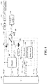
- Fig. 4 schematically shows a functional block diagram of a power circuit according to one or more examples of an embodiment of the present disclosure.
- a working principle of the switching circuit portion is the same as that in Fig. 1 . That is, the circuit working principle involving a first switch SW1 402, a second switch SW2 404, a power switch SW3 406, a control unit 408, a pulse circuit 412, and a delay circuit 414 is the same as that in Fig. 1 .
- the solution on the switching circuit portion set forth with reference to Fig. 2 and Fig. 3 also applies to one or more examples of the embodiment of Fig. 4.
- Fig. 4 differs from Fig. 1 in a charging-associated circuit portion. In order to save space, the description of the same portion will not be repeated.
- the circuit portion associated with the charging process in Fig. 4 will be described below.
- the external power source when an external power source is connected through a USB interface 420, the external power source powers a charger 416.
- output of the charger 416 is split into two portions, one portion is used for charging a battery 410, and the other portion is used for supplying power to an electrical component of the system. Compared with Fig. 1 , this is implemented by changing a connection mode of a diode D1 426 and a control terminal of the second switch SW2 404. The detailed description will be provided below.
- an anode of the diode D1 426 is connected to one output terminal of the charger 416, and a cathode of the diode is connected to a power output terminal (VCC).
- the other output terminal of the charger 416 is coupled to the battery.
- a control signal of the second switch SW2 404 is a high-level voltage signal from the other terminal of the charger.
- a part of the electrical energy outputted from the charger is used for charging the battery, and another part of the electrical energy outputted from the charger is used for supplying power to the electrical component, and in this case, the battery is disconnected from the electrical component.
- the power circuit designed in Fig. 4 still can enable the battery of the wearable device to be charged in both the power-on state and the power-off state. That is, there are two charging modes, one is a power-on charging mode, and the other is a power-off charging mode. Different values may be set for the charging parameters in the two modes. For example, the charging current in the power-on mode shall be lower than the charging current in the power-off mode, thereby reducing the temperature rise and improving the safety. To improve the safety, the power-on charging mode may have stricter temperature control. Working principles of the charging process in the power-on mode and the charging process in the power-off mode will be further described in detail below.
- the charging process in the power-on mode is as follows. For example, in the power-on state, both the first switch SW1 402 and the second switch SW2 402 are closed.
- the external power source may power the charger 416.
- An output voltage of one output terminal of the charger 416 switches on the diode D1 426, and the high-level voltage signal outputted from the other output terminal switches off the second switch SW2 404.
- the power supply of the battery 410 to the electrical component is cut off. Instead, the voltage outputted from one output terminal of the charger supplies power to the electrical component of the system through the conducting diode D1. And, the other output terminal of the charger charges the battery 410.
- the charging process in the power-off mode is as follows.
- the first switch SW1 402 and the second switch SW2 404 are both switched off.
- the external power source may power the charger 416.
- the other output terminal of the charger charges the battery 410.
- a high-level signal is still provided to the second switch SW2 404, such that the SW2 is still in an off state.
- the battery 410 is also disconnected from the electrical component in the power-off charging mode.
- Fig. 5 and Fig. 6 show schematic diagrams of implementations of example circuits corresponding to the functional block diagram of Fig. 1 , respectively. It is understandable that Fig. 5 and Fig. 6 are only schematic diagrams of implementations of example circuits given for those skilled in the art to better understand and implement the teachings of the present disclosure, rather than specific limitations to the technical solutions of the present disclosure.
- the voltage VBUS shown in the upper part of the figure is from a VBUS pin of a USB interface.
- U1 is an overvoltage protection IC, i.e., an overvoltage protection circuit OVP.
- U2 is an overcurrent protection IC, i.e., an overcurrent protection circuit OCP.
- J1 in the figure is a battery connector, and U3 is a charger.
- a battery has two NTCs.
- NTC1 is connected to MCU, and NCT2 is connected to the charger.
- the charger may communicate with the MCU via I2C.
- V3V3 is generated by a voltage regulator.
- the voltage regulator is powered by VCC.
- SW3 is a power switch.
- Pin1 is an OFF electrode
- Pin2 is an ON electrode
- Pin3 is a common electrode.
- a first switch SW1 is implemented by a field effect transistor (MOSFET_P) Q1.
- a second switch SW2 is implemented by a field effect transistor (MOSFET_P) Q2.
- a pulse circuit includes a resistor R15 and a capacitor C11.
- a duration of a pulse signal generated by the pulse circuit depends on values of the resistor R15 and the capacitor C11. For example, the duration may approximately be a value of a product of the R15 and the C11, i.e., R15 ⁇ C11.
- a delay circuit mainly includes a gate inverter U4, a field effect transistor Q3, a resistor R17, and a capacitor C9.
- Delay time of the delay circuit depends on values of the R17 and the capacitor C9. For example, the delay time may approximately be a value of a product of the R17 and the C9, i.e., R17 ⁇ C9.
- Fig. 6 shows another implementation example.
- the voltage VBUS shown in the upper part of the figure is from a VBUS pin of a USB interface.
- U1 is an overvoltage protection IC, i.e., an overvoltage protection circuit OVP.
- U2 is an overcurrent protection IC, i.e., an overcurrent protection circuit OCP.
- J1 in the figure is a battery connector, and U3 is a charger.
- a battery has two NTCs.
- NTC1 is connected to MCU, and NCT2 is connected to the charger.
- the charger may communicate with the MCU via I2C.
- V3V3 is generated by a voltage regulator.
- the voltage regulator is powered by VCC.
- SW3 is a power switch.
- Pin1 is an OFF electrode
- Pin2 is an ON electrode
- Pin3 is a common electrode.
- a first switch SW1 is implemented by a field effect transistor (MOSFET_P) Q3.
- MOSFET_P field effect transistor
- a second switch SW2 is implemented by a field effect transistor (MOSFET_P) Q4.
- MOSFET_P field effect transistor
- a pulse circuit includes a field effect transistor Q2, a field effect transistor Q6, a resistor R11, a resistor R14, a capacitor C12, a diode D1, and a diode D3.
- a duration of a pulse signal generated by the pulse circuit depends on values of the resistor R14 and the capacitor C12. For example, the duration may approximately be a value of a product of the R14 and the C12, i.e., R14 ⁇ C12.
- a delay circuit mainly includes a gate inverter U4, a field effect transistor Q1, a field effect transistor Q5, a resistor R19, and a capacitor C9.
- Delay time of the delay circuit depends on values of the R19 and the capacitor C9. For example, the delay time may approximately be a value of a product of the R19 and the C9, i.e., R19 ⁇ C9.
Landscapes
- Engineering & Computer Science (AREA)
- Power Engineering (AREA)
- Theoretical Computer Science (AREA)
- Physics & Mathematics (AREA)
- General Physics & Mathematics (AREA)
- General Engineering & Computer Science (AREA)
- Computer Hardware Design (AREA)
- Business, Economics & Management (AREA)
- Emergency Management (AREA)
- Human Computer Interaction (AREA)
- Charge And Discharge Circuits For Batteries Or The Like (AREA)
Abstract
Description
- The present disclosure generally relates to the field of wearable devices, and in particular to, a power circuit for a battery powered wearable device.
- Generally, a power circuit of a battery powered wearable device may mainly include, e.g., a battery, a charger, a voltage regulator, a USB port, and a switch. The battery powers the wearable device, and the charger is used for charging the battery via an external power source. The external power source is usually connected to the wearable device via the USB port. The voltage regulator converts a battery voltage to some voltages for system components of the wearable device. When the wearable device is powered off, the power supply is cut off by a switch.
- When an existing battery powered wearable device is switched off, usually there will be two designs. One design is that when the wearable device is powered off, the wearable device enters a sleep mode. The other design is that when the wearable device is powered off, the power supply is physically cut off. In the first design, the system components of the wearable device will still consume power in the sleep mode. In this case, the battery may be deeply discharged after certain time. In the second design, if the power supply is physically cut off, the system components of the device except for the battery itself will not consume any power. However, in this case, due to the immediate physical power-off, some UX (user interaction) functions before the device is powered off, such as power-off audio tone, cannot be implemented, nor may some data be stored. In addition, for the sake of safety, when a user is wearing and using the wearable device such as an earbud, it is often impossible to charge the wearable device.
- Therefore, an improved technical solution is required, such that when the wearable device is powered off, the system components (except for the battery itself) consume no power, while providing the UX functions and guaranteeing that data is properly stored. In addition, an improved technical solution is further required, such that the wearable device can be safely used while being charged.
- According to an aspect of the present disclosure, a power circuit for a battery powered wearable device is provided. The power circuit may include a first switch and a second switch. The first switch and the second switch are successively coupled between the battery of the wearable device and a power output terminal of the power circuit. The power circuit may further include a control unit. The control unit is configured to receive a detection signal indicating that a power switch is switched off, and send, after completing required data processing before the wearable device is powered off based on the detection signal, a first control signal to the first switch, to control the first switch to be switched off and cause the second switch to be switched off, thereby cutting off power supply of the battery via the power output terminal.
- According to one or more embodiments, the power circuit may further include a delay circuit coupled between the power switch and the first switch. The delay circuit may send, in response to the power switch being switched off and after delay time, a delay control signal to the first switch to control the first switch to be switched off and cause the second switch to be switched off, thereby cutting off the power supply of the battery via the power output terminal.
- According to one or more embodiments, the power circuit may further include a pulse circuit coupled between the power switch and the first switch. The pulse circuit may send, in response to the power switch being switched on, a pulse signal to the first switch to control the first switch to be closed and cause the second switch to be closed, such that the battery supplies power via the power output terminal.
- According to one or more embodiments, the control unit may be activated in response to the power supply of the battery, and send, after being activated, a second control signal to the first switch, such that the first switch remains closed until the power switch is switched off.
- According to one or more embodiments, the power circuit may further include a charger for charging the battery, and the control unit may set different values for a charging parameter of the charger based on whether the wearable device is in a power-on charging mode or a power-off charging mode.
- According to one or more embodiments, the control unit receives a first battery temperature detection signal, and controls a charging process based on the first battery temperature detection signal; and/or the charger receives a second battery temperature detection signal, and controls the charging process based on the second battery temperature detection signal.
- According to one or more embodiments, the power circuit may further include a diode. The diode is switched on to enable an external power source to not only supply power to the charger but also supply power to the power output terminal, where the charger charges the battery. An anode of the diode is coupled to an interface for connecting an external power source, and a cathode of the diode is coupled to the power output terminal.
- According to one or more embodiments, the power circuit further includes a diode. The diode is switched on to enable the external power source to power the charger. The charger causes the second switch to be closed while charging the battery, and thus supplies power to the power output terminal. The anode of the diode is coupled to the charger, and the cathode of the diode is coupled to the power output terminal.
- The present disclosure can be better understood by reading the following description of nonlimiting embodiments with reference to the accompanying drawings.
-
Fig. 1 schematically shows a functional block diagram of a power circuit according to one or more examples of an embodiment of the present disclosure; -
Fig. 2 schematically shows a working process of switching circuit switching of a power circuit in power-on/power-off of a wearable device according to one or more embodiments of the present disclosure; -
Fig. 3 shows a schematic diagram of charging management of the power circuit according to one or more embodiments of the present disclosure; -
Fig. 4 schematically shows a functional block diagram of the power circuit according to one or more examples of another embodiment of the present disclosure; -
Fig. 5 illustrates an example circuit corresponding to the functional block diagram ofFig. 1 ; and -
Fig. 6 illustrates another example circuit corresponding to the functional block diagram ofFig. 1 . - It should be understood that the following description of embodiments is given for illustrative purposes only, instead of limitations. The example division of functional blocks, modules, or units shown in the figures should not be construed as implying that these functional blocks, modules, or units must be implemented as physically separate units. The functional blocks, modules, or units that are shown or described may be implemented as separate units, circuits, chips, functional blocks, modules, or circuit elements. One or more functional blocks or units may also be implemented in a common circuit, chip, circuit element, or unit.
- The use of singular terms (such as, but not limited to, "a") is not intended to limit the number of items. The use of relational terms, such as, but not limited to, "top," "bottom," "left," "right," "upper part," "lower part," "downward," "upward," "side," "first," "second," ("third", etc.) "entry," "exit," and the like, for written descriptions is for clearness in specific reference to the accompanying drawings, and is not intended to limit the scope of the present disclosure or the appended claims, unless otherwise specified. The terms "couple," "coupling," "coupled," "coupler," and similar terms are widely used herein, and may include any method or apparatus on or in or to or with which an intervening element, or one or more members are fixed, combined, bonded, fastened, attached, united, inserted, formed, or communicated, or otherwise any method or apparatus which is directly or indirectly mechanically, magnetically, electrically, chemically, or operatively associated with an intervening element, or one or more members, or may include, but is not limited to, any method or apparatus in which one member is integrated with another member. The coupling may occur in any direction, including rotational occurrence. The terms "including" and "such as" are illustrative, instead of limiting. Unless otherwise stated, the term "may" means "may, but not necessarily." Although any other language may be used in the present disclosure, the embodiments shown in the accompanying drawings are examples given for purposes of illustration and explanation, and are not the only embodiments of the subject matter herein.
- In order to overcome the defects of the existing technical solutions, the present disclosure provides a power circuit for a battery powered wearable device. The power circuit includes a control switch and a control unit arranged between a battery and a power output terminal supplying power to an electrical component. The control unit may detect a power-off signal of a power switch, and when detecting the power-off signal of the power switch, first guarantees that a working system of the wearable device completes required relevant processing before power-off, such as storing data, and generating and playing a power-off audio, and then the control unit sends a control signal to the control switch to switch off the control switch, thereby completely cutting off the power supply of the battery to the electrical component via the power output terminal. The power circuit of the present disclosure not only can guarantee the timely storage of working data and the implementation of functions related to user interaction when the wearable device is switched off, but also can completely cut off power supply of the battery to the electrical component, thereby reducing power consumption of the battery. In addition, the power circuit provided in the present disclosure further can not only enable, when connecting with an external power source for charging, the control unit of the power circuit to monitor a battery temperature, but also enable a charger of the power circuit to monitor the battery temperature as well. Both the control unit and the charger can control the charging of the battery based on a monitoring result of the battery temperature, thereby improving the use safety of a user, guaranteeing that the wearable device can be safely charged while being used by the user, and further providing ease of use for the user.
- Power circuits in a plurality of examples of a plurality of embodiments of the present disclosure will be described in detail below with reference to the accompanying drawings.
Fig. 1 shows a schematic functional block diagram of a power circuit according to one or more examples of an embodiment of the present disclosure. For ease of understanding, the present disclosure divides the power circuit into two portions based on main functions for description, for example, description of a circuit portion used for switching and a portion used for charging respectively. Those skilled in the art may understand that the example schematic functional block diagram of the power circuit is provided only for contributing to clear and comprehensive understanding of the content of the present disclosure, and is not intended to limit the present disclosure. - In some embodiments, for example, the circuit portion used for switch state switching in the power circuit may mainly include a first switch (SW1) 102, a second switch (SW2) 104, a third switch (SW3) 106, and a control unit 108 (e.g., a micro control unit MCU). The third switch SW3 is a power switch. The
first switch SW1 102 and thesecond switch SW2 104 are electronic switches, e.g., may be triode switches or field effect transistor switches. Thefirst switch SW1 102 and thesecond switch SW2 104 may be coupled between abattery 110 of the power circuit and a power output terminal supplying power to an electrical component of the wearable device. In some embodiments, for example, the power output terminal supplying power to an electrical component may be connected to avoltage regulator 128 to convert a supply voltage (e.g., VCC) to a voltage for a system component of the wearable device. In some embodiments, the control unit MCU 108 may detect a state of thepower switch SW3 106, and upon receiving a detection signal (e.g., PWR_OFF_DET) indicating that the power switch is switched off, first executes required system processing before the device is powered off, and then sends a control signal (e.g., PWR_OFF) to thefirst switch SW1 102, where the control signal may control the first switch SW1 to be switched off, thereby cutting off the power supply of thebattery 110 to the electrical component of the system via the power output terminal. In this case, the second switch SW2 may be switched off accordingly following the first switch SW2. - In some embodiments, the circuit portion for switching in the power circuit may include a
pulse circuit 112. Thepulse circuit 112 is coupled between thepower switch SW3 106 and thefirst switch SW1 102, and sends, in response to thepower switch 106 being switched on, a pulse signal to thefirst switch SW1 102 to control thefirst switch SW1 102 to be closed. In some embodiments, the circuit portion for switching in the power circuit further includes adelay circuit 114. Thedelay circuit 114 is coupled between thepower switch SW3 106 and thefirst switch SW1 102 to send, in response to thepower switch 106 being switched off for a period of delay time, a control signal to thefirst switch SW1 102 to control thefirst switch SW1 102 to be switched off. -
Fig. 2 shows a working process of the power circuit in power-on and power-off of a wearable device according to one or more embodiments of the present disclosure. Working processes of a circuit portion for switching in the power circuit in a power-on process and a power-off process of the wearable device will be further described below respectively with reference toFig. 1 andFig. 2 . - For example, in the power-on process of the wearable device, when the
power switch SW3 106 is switched on, thepulse circuit 112 will output a pulse signal to thefirst switch SW1 102. After receiving the pulse signal, thefirst switch SW1 102 will be closed. After thefirst switch SW1 102 is switched off, and when no external power source is connected through, for example, aUSB interface 120, thesecond switch SW2 104 will be switched off accordingly following thefirst switch SW1 102. Then, thebattery 110 will power an electrical component of the system. Due to the closure of thefirst switch SW1 102 and thesecond switch SW2 104, a battery voltage VBAT is provided to the power output terminal, and the power output terminal may supply power to a system component of the wearable device with a supply voltage VCC to start the system. After the system of the wearable device is started, the control unit MCU 108 will start to work and output a control signal (PWR_ON), such that the first switch SW1 remains closed until the wearable device is switched off again. In this case, the wearable device completes the power-on process. A duration of the pulse signal generated by thepulse circuit 112 may be equal to or longer than system startup time of the wearable device. - For example, in the power-off process of the wearable device, when the
power switch SW3 106 is switched off (the power switch SW3 is switched from ON to OFF), the control unit MCU 108 will detect a signal indicating that the power switch is switched off, such as a PWR_OFF_DET signal. In this case, before the power-off, the control unit MCU 108 will execute some required processing, e.g., UX-related processing or processing such as storing data. For example, before the power-off, an earbud will play a power-off audio tone. After completing processing operations similar to the above, the MCU 108 will send a PWR_OFF signal to switch off thefirst switch SW1 102. Then, thesecond switch SW2 104 is also switched off, thereby cutting off power supply of thebattery 110 to the electrical component of the system via the power output terminal, i.e., disconnecting a VCC terminal from a VBAT terminal. In this case, all components of the system, except for the battery itself, are completely powered off, thereby avoiding further consumption of battery power. The battery level may be notified to the control unit MCU 108 based on a VBAT_LEVEL signal. In some embodiments, thedelay circuit 114 may be further arranged to send, after thepower switch SW3 106 is switched off for a period of time (e.g., delay time), a control signal to thefirst switch SW1 104 to control thefirst switch SW1 104 to be switched off. The delay circuit may be arranged to guarantee that thefirst switch SW1 104 is switched off after a period of delay time when the control unit MCU 108 may not be able to switch off thefirst switch SW1 104. That is to say, the delay circuit may guarantee, in the case of software power-off failure, the complete power-off of the wearable device by hardware power-off, i.e., guarantee that all system components except for the battery no longer consume power. In some embodiments, the delay time may be set to be equal to or longer than the system power-off time. - Further referring to
Fig. 1 , the circuit portion for charging in the power circuit will be further described below. For example, the charging process may mainly involve acharger 116, the control unit MCU 108, a NTC 118 (e.g., a negative temperature coefficient sensing device), thefirst switch SW1 102, thesecond switch SW2 104, and adiode D1 126. An anode of thediode D1 126 is coupled to the interface (e.g., the USB interface) 120, and a cathode of the diode is coupled to the power output terminal VCC. - For example, as shown in the figures, the power circuit may be connected to an external power source through the
USB interface 120 to charge thebattery 110. VBUS is a voltage provided by the external power source via theUSB interface 120. When the external power source is connected via theUSB interface 120, the VUSB will output a high-level signal as a control signal to switch off thesecond switch SW2 104, thereby cutting off the power supply of thebattery 110. At the same time, thediode D1 126 connected between theUSB interface 120 and the power output terminal VCC is switched on. Thus, the external power source will power the electrical component of the system of the wearable device by switching on thediode D1 126. - In some examples, an overvoltage
protection circuit OVP 122 and an overcurrentprotection circuit OCP 124 may also be provided between theUSB interface 120 and thecharger 116, such that the external power source may power thecharger 116 through the overvoltageprotection circuit OVP 122 and the overcurrentprotection circuit OCP 124. For example, the overvoltageprotection circuit OVP 122 may be an IC for overvoltage protection. The overcurrentprotection circuit OCP 124 may be an IC for overcurrent protection. In some examples, the overvoltageprotection circuit OVP 122 and the overcurrentprotection circuit OCP 124 may be provided between the anode of thediode D1 126 and theUSB interface 120. Once the voltage VBUS provided by the external power source is higher than an overvoltage threshold, or a current provided by the external power source is higher than an overcurrent threshold, a connection between the power circuit and the external power source is cut off, i.e., a power supply connection between the external power source and the charger and a power supply connection between the external power source and the electrical component of the system are both cut off. For example, referring toFig. 1 , the VBUS will be disconnected from the VUSB, and the VBUS will be disconnected from the VCC. - For example, the control unit MCU 108 may detect whether an external power source is plugged into the
USB interface 120 based on the USB detection signal (USB_DET). In addition, the control unit MCU 108 may communicate with thecharger 116 based on I2C, SPI, GPIO or other protocols. The control unit MCU 108 may set a charging parameter and control the charging. - Both the control unit MCU 108 and the
charger 116 monitor the battery temperature based on theNTC 118. For example, aNTC 116 may be driven by a current source or driven by a voltage source. If theNTC 116 is driven by a current source, one NTC is enough. If theNTC 116 is driven by a voltage source, it is necessary to set two NTCs. Both the control unit MCU 108 and thecharger 116 may control the charging process based on the monitored battery temperature. For example, theNTC 118 may provide battery temperature detection signals, e.g., BAT_TEMP1 and BAT_TEMP2, to the control unit MCU 108 and thecharger 116, respectively. Based on the battery temperature detection signals, both the control unit MCU108 and thecharger 116 may control the charging process. The charging process may be enabled or disabled, and different charging parameters, such as charging current, may be set based on the battery temperature. - The power circuit designed in the present disclosure can enable the battery of the wearable device to be charged in both a power-on state and a power-off state. That is, there are two charging modes, one is a power-on charging mode, and the other is a power-off charging mode. Different values may be set for the charging parameter in the two modes. For example, the charging current in the power-on mode shall be lower than the charging current in the power-off mode, thereby reducing the temperature rise and improving the safety. To improve the safety, the power-on charging mode may have stricter temperature control. The charging process in the power-on mode and the charging process in the power-off mode will be further described in detail below respectively.
- The charging process in the power-on mode is as follows. For example, in the power-on state, both the
first switch SW1 102 and thesecond switch SW2 104 are closed. When connected to the external power source through theUSB interface 120, thesecond switch SW2 104 is switched off under the control of a high-level control signal, thereby cutting off the power supply of thebattery 110 to the electrical component of the system via the power output terminal. When the power circuit is connected to the external power source through theUSB interface 120, thediode D1 126 is switched on, and then the external power source may power the electrical component of the system via theUSB interface 120, theOVP 122 and the OCP 124 (one or both of the two may be selected based on actual needs), thediode D1 126, and the voltage stabilizer 128 (optionally provided as required). Further, the external power source may power thecharger 116 through theUSB interface 120, theOVP 122, and theOCP 124. Thecharger 116 charges the battery. - The charging process in the power-off mode is as follows. For example, in the power-off state, the
first switch SW1 102 and thesecond switch SW2 104 are both disconnected, and the external power source can power thecharger 116 only through theUSB interface 120, theOVP 122 and the OCP 124 (one or both of the two may be selected based on actual needs). An output terminal of thecharger 116 outputs electric energy, thus charging thebattery 110. In this case, thebattery 110 is disconnected from the electrical component of the system, thus failing to power the electrical component of the system. -
Fig. 3 shows a schematic diagram of charging management of the power circuit according to one or more embodiments of the present disclosure.Fig. 3 shows different management of charging processes when the wearable device is in a power-on state and in a power-off state, respectively. In a power-on charging mode and a power-off charging mode, charging parameters are set respectively, and different charging management is performed for the power-on charging mode and the power-off charging mode based on different management conditions. - For example, the charging parameters may include, but are not limited to, a charging voltage parameter, a pre-charging current parameter, a charging termination current parameter, a recharging threshold voltage parameter, a charging safety timer parameter, a pre-charging safety timer parameter, and the like.
- As shown in
Fig. 3 , in the power-on charging mode, the battery temperature is monitored based on NTC. For example, when the temperature is lower than 0 °C, charging is disabled. When the temperature is higher than 0 °C and lower than 10 °C, the charging current may be set as 0.1C. When the temperature is higher than 10 °C and lower than 40 °C, the charging current may be set as 0.2C. When the temperature is higher than 40 °C and lower than 45 °C, the charging current may be set as 0.1C. When the temperature is higher than 45 °C, charging may be disabled. - In the power-off charging mode, the battery temperature is monitored based on the NTC. For example, when the temperature is lower than 0 °C, charging is disabled. When the temperature is higher than 0 °C and lower than 10 °C, the charging current may be set as 0.2C. When the temperature is higher than 10 °C and lower than 45 °C, the charging current may be set as 0.8C. When the temperature is higher than 45 °C, charging may be disabled.
-
Fig. 4 schematically shows a functional block diagram of a power circuit according to one or more examples of an embodiment of the present disclosure. InFig. 4 , a working principle of the switching circuit portion is the same as that inFig. 1 . That is, the circuit working principle involving afirst switch SW1 402, asecond switch SW2 404, apower switch SW3 406, acontrol unit 408, apulse circuit 412, and adelay circuit 414 is the same as that inFig. 1 . The solution on the switching circuit portion set forth with reference toFig. 2 andFig. 3 also applies to one or more examples of the embodiment ofFig. 4. Fig. 4 differs fromFig. 1 in a charging-associated circuit portion. In order to save space, the description of the same portion will not be repeated. The circuit portion associated with the charging process inFig. 4 will be described below. - In the embodiment shown in
Fig. 4 , when an external power source is connected through aUSB interface 420, the external power source powers acharger 416. In one or more examples of the embodiment ofFig. 4 , output of thecharger 416 is split into two portions, one portion is used for charging a battery 410, and the other portion is used for supplying power to an electrical component of the system. Compared withFig. 1 , this is implemented by changing a connection mode of adiode D1 426 and a control terminal of thesecond switch SW2 404. The detailed description will be provided below. - Specifically, for example, an anode of the
diode D1 426 is connected to one output terminal of thecharger 416, and a cathode of the diode is connected to a power output terminal (VCC). The other output terminal of thecharger 416 is coupled to the battery. Further, a control signal of thesecond switch SW2 404 is a high-level voltage signal from the other terminal of the charger. When the external power source charges the wearable device through theUSB interface 420, a voltage VBUS provided by the external power source contributes the charger to outputting a high-level voltage through anOVP 422 and anOCP 424, and the outputted high-level voltage switches off thesecond switch SW2 404 and switches on the diode D1. Therefore, in the power-on state, a part of the electrical energy outputted from the charger is used for charging the battery, and another part of the electrical energy outputted from the charger is used for supplying power to the electrical component, and in this case, the battery is disconnected from the electrical component. - The power circuit designed in
Fig. 4 still can enable the battery of the wearable device to be charged in both the power-on state and the power-off state. That is, there are two charging modes, one is a power-on charging mode, and the other is a power-off charging mode. Different values may be set for the charging parameters in the two modes. For example, the charging current in the power-on mode shall be lower than the charging current in the power-off mode, thereby reducing the temperature rise and improving the safety. To improve the safety, the power-on charging mode may have stricter temperature control. Working principles of the charging process in the power-on mode and the charging process in the power-off mode will be further described in detail below. - The charging process in the power-on mode is as follows. For example, in the power-on state, both the
first switch SW1 402 and thesecond switch SW2 402 are closed. When the external power source is connected through theUSB interface 420, the external power source may power thecharger 416. An output voltage of one output terminal of thecharger 416 switches on thediode D1 426, and the high-level voltage signal outputted from the other output terminal switches off thesecond switch SW2 404. In this case, the power supply of the battery 410 to the electrical component is cut off. Instead, the voltage outputted from one output terminal of the charger supplies power to the electrical component of the system through the conducting diode D1. And, the other output terminal of the charger charges the battery 410. - The charging process in the power-off mode is as follows. In the power-off state, the
first switch SW1 402 and thesecond switch SW2 404 are both switched off. When the external power source is connected through theUSB interface 420, the external power source may power thecharger 416. The other output terminal of the charger charges the battery 410. In this case, a high-level signal is still provided to thesecond switch SW2 404, such that the SW2 is still in an off state. The battery 410 is also disconnected from the electrical component in the power-off charging mode. -
Fig. 5 andFig. 6 show schematic diagrams of implementations of example circuits corresponding to the functional block diagram ofFig. 1 , respectively. It is understandable thatFig. 5 andFig. 6 are only schematic diagrams of implementations of example circuits given for those skilled in the art to better understand and implement the teachings of the present disclosure, rather than specific limitations to the technical solutions of the present disclosure. - For example, referring to the example of
Fig. 5 , the voltage VBUS shown in the upper part of the figure is from a VBUS pin of a USB interface. U1 is an overvoltage protection IC, i.e., an overvoltage protection circuit OVP. U2 is an overcurrent protection IC, i.e., an overcurrent protection circuit OCP. J1 in the figure is a battery connector, and U3 is a charger. In the implementation ofFig. 5 , a battery has two NTCs. For example, NTC1 is connected to MCU, and NCT2 is connected to the charger. The charger may communicate with the MCU via I2C. V3V3 is generated by a voltage regulator. The voltage regulator is powered by VCC. SW3 is a power switch. For example, in the SW3, Pin1 is an OFF electrode, Pin2 is an ON electrode, and Pin3 is a common electrode. - In the lower part of
Fig. 5 , several dashed blocks are shown. For example, enclosed by a dashedblock 502, a first switch SW1 is implemented by a field effect transistor (MOSFET_P) Q1. Enclosed by a dashed block 504, a second switch SW2 is implemented by a field effect transistor (MOSFET_P) Q2. - Enclosed by a dashed block 506, a pulse circuit includes a resistor R15 and a capacitor C11. A duration of a pulse signal generated by the pulse circuit depends on values of the resistor R15 and the capacitor C11. For example, the duration may approximately be a value of a product of the R15 and the C11, i.e., R15∗C11.
- Enclosed by a dashed
block 508, a delay circuit mainly includes a gate inverter U4, a field effect transistor Q3, a resistor R17, and a capacitor C9. Delay time of the delay circuit depends on values of the R17 and the capacitor C9. For example, the delay time may approximately be a value of a product of the R17 and the C9, i.e., R17∗C9. -
Fig. 6 shows another implementation example. For example, referring to the example ofFig. 6 , the voltage VBUS shown in the upper part of the figure is from a VBUS pin of a USB interface. U1 is an overvoltage protection IC, i.e., an overvoltage protection circuit OVP. U2 is an overcurrent protection IC, i.e., an overcurrent protection circuit OCP. J1 in the figure is a battery connector, and U3 is a charger. In the implementation ofFig. 6 , a battery has two NTCs. For example, NTC1 is connected to MCU, and NCT2 is connected to the charger. The charger may communicate with the MCU via I2C. V3V3 is generated by a voltage regulator. The voltage regulator is powered by VCC. SW3 is a power switch. For example, in the SW3, Pin1 is an OFF electrode, Pin2 is an ON electrode, and Pin3 is a common electrode. - In the lower part of
Fig. 6 , several dashed blocks are shown. For example, enclosed by a dashedblock 602, a first switch SW1 is implemented by a field effect transistor (MOSFET_P) Q3. - Enclosed by a dashed
block 604, a second switch SW2 is implemented by a field effect transistor (MOSFET_P) Q4. - Enclosed by a dashed block 606, a pulse circuit includes a field effect transistor Q2, a field effect transistor Q6, a resistor R11, a resistor R14, a capacitor C12, a diode D1, and a diode D3. A duration of a pulse signal generated by the pulse circuit depends on values of the resistor R14 and the capacitor C12. For example, the duration may approximately be a value of a product of the R14 and the C12, i.e., R14∗C12.
- Enclosed by a dashed
block 608, a delay circuit mainly includes a gate inverter U4, a field effect transistor Q1, a field effect transistor Q5, a resistor R19, and a capacitor C9. Delay time of the delay circuit depends on values of the R19 and the capacitor C9. For example, the delay time may approximately be a value of a product of the R19 and the C9, i.e., R19∗C9. -
- Example 1. A power circuit for a battery powered wearable device, comprising:
- a first switch and a second switch successively coupled between the battery of the wearable device and a power output terminal of the power circuit; and
- a control unit configured to receive a detection signal indicating that a power switch is switched off, and send, after completing required data processing before the wearable device is powered off based on the detection signal, a first control signal to the first switch, to control the first switch to be switched off and cause the second switch to be switched off, thereby cutting off power supply of the battery via the power output terminal.
- Example 2. The power circuit according to example 1, further comprising a delay circuit coupled between the power switch and the first switch, wherein the delay circuit sends, in response to the power switch being switched off and after delay time, a delay control signal to the first switch to control the first switch to be switched off and cause the second switch to be switched off, thereby cutting off the power supply of the battery via the power output terminal.
- Example 3. The power circuit according to example 1 or 2, further comprising a pulse circuit coupled between the power switch and the first switch, wherein the pulse circuit sends, in response to the power switch being switched on, a pulse signal to the first switch to control the first switch to be closed and cause the second switch to be closed, such that the battery supplies power via the power output terminal.
- Example 4. The power circuit according to example 3, wherein the control unit is activated in response to the power supply of the battery, and sends, after being activated, a second control signal to the first switch, such that the first switch remains closed until the power switch is switched off.
- Example 5. The power circuit according to example 1 or 2, further comprising a charger for charging the battery, and the control unit setting different values for a charging parameter of the charger based on whether the wearable device is in a power-on charging mode or a power-off charging mode.
- Example 6. The power circuit according to example 5, wherein
- the control unit receives a first battery temperature detection signal, and controls a charging process based on the first battery temperature detection signal; and/or
- the charger receives a second battery temperature detection signal, and controls the charging process based on the second battery temperature detection signal.
- Example 7. The power circuit according to example 6, further comprising a diode, wherein the diode is switched on to enable an external power source to not only supply power to the charger but also supply power to the power output terminal, wherein the charger charges the battery.
- Example 8. The power circuit according to example 7, wherein an anode of the diode is coupled to an interface for connecting an external power source, and a cathode of the diode is coupled to the power output terminal.
- Example 9. The power circuit according to example 6, further comprising a diode, wherein the diode is switched on to enable an external power source to power the charger, and the charger causes the second switch to be closed while charging the battery, and thus supplies power to the power output terminal.
- Example 10. The power circuit according to example 9, wherein the anode of the diode is coupled to the charger, and the cathode of the diode is coupled to the power output terminal.
- The description of embodiments has been presented for the purposes of illustration and description. Appropriate modifications and alterations to the embodiments may be executed in light of the above description, or may be acquired by practice. The described methods and associated actions may also be executed in various sequences other than the sequence described herein, in parallel, and/or concurrently. The described system is essentially an example, and may include additional elements and/or omit elements. The subject matter of the present disclosure includes all novel and non-obvious combinations of the various disclosed systems and configurations and additional features, functions, and/or properties.
- As used herein, an element or step recited in a singular form and preceded by a word "a/an" should be understood as not excluding a plurality of said elements or steps, unless such exclusion is indicated. Further, the reference to "an embodiment" or "an example" of the present disclosure is not intended to be interpreted as excluding the existence of additional embodiments that also incorporate the recited features. The present disclosure has been described above with reference to particular embodiments. However, as will be appreciated by those of ordinary skills in the art, various modifications and alterations may be made to the present disclosure without departing from the broad spirit and scope of the present disclosure as set forth in the appended claims.
Claims (10)
- A power circuit for a battery powered wearable device, comprising:a first switch and a second switch successively coupled between the battery of the wearable device and a power output terminal of the power circuit; anda control unit configured to receive a detection signal indicating that a power switch is switched off, and send, after completing required data processing before the wearable device is powered off based on the detection signal, a first control signal to the first switch, to control the first switch to be switched off and cause the second switch to be switched off, thereby cutting off power supply of the battery via the power output terminal.
- The power circuit according to claim 1, further comprising a delay circuit coupled between the power switch and the first switch, wherein the delay circuit sends, in response to the power switch being switched off and after delay time, a delay control signal to the first switch to control the first switch to be switched off and cause the second switch to be switched off, thereby cutting off the power supply of the battery via the power output terminal.
- The power circuit according to claim 1 or 2, further comprising a pulse circuit coupled between the power switch and the first switch, wherein the pulse circuit sends, in response to the power switch being switched on, a pulse signal to the first switch to control the first switch to be closed and cause the second switch to be closed, such that the battery supplies power via the power output terminal.
- The power circuit according to claim 3, wherein the control unit is activated in response to the power supply of the battery, and sends, after being activated, a second control signal to the first switch, such that the first switch remains closed until the power switch is switched off.
- The power circuit according to claim 1 or 2, further comprising a charger for charging the battery, and the control unit setting different values for a charging parameter of the charger based on whether the wearable device is in a power-on charging mode or a power-off charging mode.
- The power circuit according to claim 5, whereinthe control unit receives a first battery temperature detection signal, and controls a charging process based on the first battery temperature detection signal; and/orthe charger receives a second battery temperature detection signal, and controls the charging process based on the second battery temperature detection signal.
- The power circuit according to claim 6, further comprising a diode, wherein the diode is switched on to enable an external power source to not only supply power to the charger but also supply power to the power output terminal, wherein the charger charges the battery.
- The power circuit according to claim 7, wherein an anode of the diode is coupled to an interface for connecting an external power source, and a cathode of the diode is coupled to the power output terminal.
- The power circuit according to claim 6, further comprising a diode, wherein the diode is switched on to enable an external power source to power the charger, and the charger causes the second switch to be closed while charging the battery, and thus supplies power to the power output terminal.
- The power circuit according to claim 9, wherein the anode of the diode is coupled to the charger, and the cathode of the diode is coupled to the power output terminal.
Applications Claiming Priority (1)
| Application Number | Priority Date | Filing Date | Title |
|---|---|---|---|
| CN202110463469.9A CN115241941A (en) | 2021-04-23 | 2021-04-23 | Power supply circuit for battery powered wearable device |
Publications (1)
| Publication Number | Publication Date |
|---|---|
| EP4080723A1 true EP4080723A1 (en) | 2022-10-26 |
Family
ID=81346119
Family Applications (1)
| Application Number | Title | Priority Date | Filing Date |
|---|---|---|---|
| EP22169219.7A Pending EP4080723A1 (en) | 2021-04-23 | 2022-04-21 | Power circuit for battery powered wearable device |
Country Status (4)
| Country | Link |
|---|---|
| US (1) | US20220344948A1 (en) |
| EP (1) | EP4080723A1 (en) |
| KR (1) | KR20220146339A (en) |
| CN (1) | CN115241941A (en) |
Citations (8)
| Publication number | Priority date | Publication date | Assignee | Title |
|---|---|---|---|---|
| US20010007417A1 (en) * | 1998-02-20 | 2001-07-12 | Seiya Kitagawa | Power supply apparatus with chargeable battery and charge/discharge method |
| US20070120525A1 (en) * | 2005-11-30 | 2007-05-31 | Hiroyuki Tsuji | Electronic device with auxiliary unit that is usable detached from main unit of electronic device |
| JP2014036531A (en) * | 2012-08-09 | 2014-02-24 | Sharp Corp | Battery power supply device and electronic apparatus |
| CN104111719A (en) * | 2014-06-25 | 2014-10-22 | 小米科技有限责任公司 | Method and device for controlling battery to be disconnected from main equipment |
| US20160064958A1 (en) * | 2014-09-02 | 2016-03-03 | Samsung Electronics Co., Ltd. | Method and apparatus for battery charging |
| US20170179746A1 (en) * | 2015-12-09 | 2017-06-22 | Le Holdings (Beijing) Co., Ltd. | Battery shutdown method and device and mobile terminal |
| US20180026438A1 (en) * | 2015-04-03 | 2018-01-25 | Shanghai Sim-Bcd Semiconductor Manufacturing Co., Ltd. | Embedded battery protection system |
| CN105629825B (en) * | 2015-11-17 | 2018-10-30 | 深圳市沃特沃德股份有限公司 | A kind of management method and management system of wearable smart machine power-supply system |
Family Cites Families (4)
| Publication number | Priority date | Publication date | Assignee | Title |
|---|---|---|---|---|
| JP5427521B2 (en) * | 2009-09-04 | 2014-02-26 | 株式会社マキタ | Battery pack |
| KR102365769B1 (en) * | 2014-12-04 | 2022-02-21 | 삼성전자주식회사 | Method and apparatus for cutting off dark current in battery management system |
| WO2019187848A1 (en) * | 2018-03-30 | 2019-10-03 | 工機ホールディングス株式会社 | Work device |
| US11349474B1 (en) * | 2021-03-23 | 2022-05-31 | Infineon Technologies Austria Ag | Cascaded gate driver outputs for power conversion circuits |
-
2021
- 2021-04-23 CN CN202110463469.9A patent/CN115241941A/en active Pending
-
2022
- 2022-04-20 US US17/659,989 patent/US20220344948A1/en active Pending
- 2022-04-21 EP EP22169219.7A patent/EP4080723A1/en active Pending
- 2022-04-21 KR KR1020220049243A patent/KR20220146339A/en active Pending
Patent Citations (8)
| Publication number | Priority date | Publication date | Assignee | Title |
|---|---|---|---|---|
| US20010007417A1 (en) * | 1998-02-20 | 2001-07-12 | Seiya Kitagawa | Power supply apparatus with chargeable battery and charge/discharge method |
| US20070120525A1 (en) * | 2005-11-30 | 2007-05-31 | Hiroyuki Tsuji | Electronic device with auxiliary unit that is usable detached from main unit of electronic device |
| JP2014036531A (en) * | 2012-08-09 | 2014-02-24 | Sharp Corp | Battery power supply device and electronic apparatus |
| CN104111719A (en) * | 2014-06-25 | 2014-10-22 | 小米科技有限责任公司 | Method and device for controlling battery to be disconnected from main equipment |
| US20160064958A1 (en) * | 2014-09-02 | 2016-03-03 | Samsung Electronics Co., Ltd. | Method and apparatus for battery charging |
| US20180026438A1 (en) * | 2015-04-03 | 2018-01-25 | Shanghai Sim-Bcd Semiconductor Manufacturing Co., Ltd. | Embedded battery protection system |
| CN105629825B (en) * | 2015-11-17 | 2018-10-30 | 深圳市沃特沃德股份有限公司 | A kind of management method and management system of wearable smart machine power-supply system |
| US20170179746A1 (en) * | 2015-12-09 | 2017-06-22 | Le Holdings (Beijing) Co., Ltd. | Battery shutdown method and device and mobile terminal |
Also Published As
| Publication number | Publication date |
|---|---|
| KR20220146339A (en) | 2022-11-01 |
| US20220344948A1 (en) | 2022-10-27 |
| CN115241941A (en) | 2022-10-25 |
Similar Documents
| Publication | Publication Date | Title |
|---|---|---|
| KR100193736B1 (en) | Battery pack with battery protection | |
| US7795842B2 (en) | Adjustable cut-off voltage for mobile device battery | |
| CN115085325A (en) | Battery protection chip, battery pack and electronic device | |
| US20050007711A1 (en) | Power adapter interface circuitry for protecting a battery operated system | |
| CN112039153A (en) | On-chip system, battery pack and electronic device | |
| CN111987772A (en) | A system-on-chip, battery assembly and electronic device | |
| CN113474965A (en) | Intelligent connecting device, starting power supply and storage battery clamp | |
| JP2012039701A (en) | Battery pack and overcurrent detection method | |
| CN111987773B (en) | On-chip system, battery pack and electronic device | |
| CN111987771A (en) | On-chip system, battery pack and electronic device | |
| EP4080723A1 (en) | Power circuit for battery powered wearable device | |
| CN216056797U (en) | Output circuit, starting power supply device and battery clamp device | |
| CN103124097A (en) | Intelligent lithium ion charger | |
| CN103107577B (en) | Battery management circuit and terminal | |
| CN119561218A (en) | Control circuit and control method for realizing fast startup based on supercapacitor | |
| CN214337577U (en) | A power supply circuit for a mobile terminal and the mobile terminal | |
| KR102765888B1 (en) | Temperature monitoring apparatus for battery | |
| EP3985462B1 (en) | Battery power-on circuit | |
| CN216751251U (en) | Lithium battery power supply system and electric vehicle | |
| CN215528627U (en) | Smart Links, Starter Power and Battery Clips | |
| WO2023184067A1 (en) | Power supply circuit, battery management system, battery pack and electronic apparatus | |
| CN102104245B (en) | Method and system for protecting power battery | |
| CN223309582U (en) | Battery protection circuit, battery protection board, battery assembly and electronic device | |
| CN222852036U (en) | USB charging circuit and computer | |
| CN219496914U (en) | Intelligent watch capable of lighting screen by charging after battery is over-discharged |
Legal Events
| Date | Code | Title | Description |
|---|---|---|---|
| PUAI | Public reference made under article 153(3) epc to a published international application that has entered the european phase |
Free format text: ORIGINAL CODE: 0009012 |
|
| STAA | Information on the status of an ep patent application or granted ep patent |
Free format text: STATUS: THE APPLICATION HAS BEEN PUBLISHED |
|
| AK | Designated contracting states |
Kind code of ref document: A1 Designated state(s): AL AT BE BG CH CY CZ DE DK EE ES FI FR GB GR HR HU IE IS IT LI LT LU LV MC MK MT NL NO PL PT RO RS SE SI SK SM TR |
|
| STAA | Information on the status of an ep patent application or granted ep patent |
Free format text: STATUS: REQUEST FOR EXAMINATION WAS MADE |
|
| 17P | Request for examination filed |
Effective date: 20230313 |
|
| RBV | Designated contracting states (corrected) |
Designated state(s): AL AT BE BG CH CY CZ DE DK EE ES FI FR GB GR HR HU IE IS IT LI LT LU LV MC MK MT NL NO PL PT RO RS SE SI SK SM TR |