EP4080583A1 - Semiconductor device and method of making a semiconductor device - Google Patents
Semiconductor device and method of making a semiconductor device Download PDFInfo
- Publication number
- EP4080583A1 EP4080583A1 EP22161830.9A EP22161830A EP4080583A1 EP 4080583 A1 EP4080583 A1 EP 4080583A1 EP 22161830 A EP22161830 A EP 22161830A EP 4080583 A1 EP4080583 A1 EP 4080583A1
- Authority
- EP
- European Patent Office
- Prior art keywords
- spacer
- gate
- proximal
- distal
- spacer portion
- Prior art date
- Legal status (The legal status is an assumption and is not a legal conclusion. Google has not performed a legal analysis and makes no representation as to the accuracy of the status listed.)
- Pending
Links
Images


Classifications
-
- H—ELECTRICITY
- H10—SEMICONDUCTOR DEVICES; ELECTRIC SOLID-STATE DEVICES NOT OTHERWISE PROVIDED FOR
- H10D—INORGANIC ELECTRIC SEMICONDUCTOR DEVICES
- H10D30/00—Field-effect transistors [FET]
- H10D30/01—Manufacture or treatment
- H10D30/021—Manufacture or treatment of FETs having insulated gates [IGFET]
- H10D30/0221—Manufacture or treatment of FETs having insulated gates [IGFET] having asymmetry in the channel direction, e.g. lateral high-voltage MISFETs having drain offset region or extended-drain MOSFETs [EDMOS]
-
- H—ELECTRICITY
- H10—SEMICONDUCTOR DEVICES; ELECTRIC SOLID-STATE DEVICES NOT OTHERWISE PROVIDED FOR
- H10D—INORGANIC ELECTRIC SEMICONDUCTOR DEVICES
- H10D30/00—Field-effect transistors [FET]
- H10D30/01—Manufacture or treatment
- H10D30/021—Manufacture or treatment of FETs having insulated gates [IGFET]
- H10D30/028—Manufacture or treatment of FETs having insulated gates [IGFET] of double-diffused metal oxide semiconductor [DMOS] FETs
- H10D30/0281—Manufacture or treatment of FETs having insulated gates [IGFET] of double-diffused metal oxide semiconductor [DMOS] FETs of lateral DMOS [LDMOS] FETs
-
- H—ELECTRICITY
- H10—SEMICONDUCTOR DEVICES; ELECTRIC SOLID-STATE DEVICES NOT OTHERWISE PROVIDED FOR
- H10D—INORGANIC ELECTRIC SEMICONDUCTOR DEVICES
- H10D30/00—Field-effect transistors [FET]
- H10D30/60—Insulated-gate field-effect transistors [IGFET]
- H10D30/601—Insulated-gate field-effect transistors [IGFET] having lightly-doped drain or source extensions, e.g. LDD IGFETs or DDD IGFETs
- H10D30/603—Insulated-gate field-effect transistors [IGFET] having lightly-doped drain or source extensions, e.g. LDD IGFETs or DDD IGFETs having asymmetry in the channel direction, e.g. lateral high-voltage MISFETs having drain offset region or extended drain IGFETs [EDMOS]
-
- H—ELECTRICITY
- H10—SEMICONDUCTOR DEVICES; ELECTRIC SOLID-STATE DEVICES NOT OTHERWISE PROVIDED FOR
- H10D—INORGANIC ELECTRIC SEMICONDUCTOR DEVICES
- H10D30/00—Field-effect transistors [FET]
- H10D30/60—Insulated-gate field-effect transistors [IGFET]
- H10D30/64—Double-diffused metal-oxide semiconductor [DMOS] FETs
- H10D30/65—Lateral DMOS [LDMOS] FETs
-
- H—ELECTRICITY
- H10—SEMICONDUCTOR DEVICES; ELECTRIC SOLID-STATE DEVICES NOT OTHERWISE PROVIDED FOR
- H10D—INORGANIC ELECTRIC SEMICONDUCTOR DEVICES
- H10D62/00—Semiconductor bodies, or regions thereof, of devices having potential barriers
- H10D62/10—Shapes, relative sizes or dispositions of the regions of the semiconductor bodies; Shapes of the semiconductor bodies
- H10D62/102—Constructional design considerations for preventing surface leakage or controlling electric field concentration
- H10D62/103—Constructional design considerations for preventing surface leakage or controlling electric field concentration for increasing or controlling the breakdown voltage of reverse-biased devices
-
- H—ELECTRICITY
- H10—SEMICONDUCTOR DEVICES; ELECTRIC SOLID-STATE DEVICES NOT OTHERWISE PROVIDED FOR
- H10D—INORGANIC ELECTRIC SEMICONDUCTOR DEVICES
- H10D64/00—Electrodes of devices having potential barriers
- H10D64/01—Manufacture or treatment
- H10D64/013—Manufacture or treatment of electrodes having a conductor capacitively coupled to a semiconductor by an insulator
- H10D64/01302—Manufacture or treatment of electrodes having a conductor capacitively coupled to a semiconductor by an insulator the insulator being formed after the semiconductor body, the semiconductor being silicon
- H10D64/01354—Manufacture or treatment of electrodes having a conductor capacitively coupled to a semiconductor by an insulator the insulator being formed after the semiconductor body, the semiconductor being silicon passivation or protection of the electrode, e.g. using re-oxidation
-
- H—ELECTRICITY
- H10—SEMICONDUCTOR DEVICES; ELECTRIC SOLID-STATE DEVICES NOT OTHERWISE PROVIDED FOR
- H10D—INORGANIC ELECTRIC SEMICONDUCTOR DEVICES
- H10D64/00—Electrodes of devices having potential barriers
- H10D64/01—Manufacture or treatment
- H10D64/015—Manufacture or treatment removing at least parts of gate spacers, e.g. disposable spacers
-
- H—ELECTRICITY
- H10—SEMICONDUCTOR DEVICES; ELECTRIC SOLID-STATE DEVICES NOT OTHERWISE PROVIDED FOR
- H10D—INORGANIC ELECTRIC SEMICONDUCTOR DEVICES
- H10D64/00—Electrodes of devices having potential barriers
- H10D64/01—Manufacture or treatment
- H10D64/021—Manufacture or treatment using multiple gate spacer layers, e.g. bilayered sidewall spacers
Definitions
- the present specification relates to a laterally-diffused metal-oxide semiconductor, "LDMOS”, device and to a method of making a laterally-diffused metal-oxide semiconductor, "LDMOS", device.
- LDMOS laterally-diffused metal-oxide semiconductor
- LDMOS laterally-diffused metal-oxide semiconductor
- the method may include:
- the method may include removing the sacrificial gate portion after forming the second spacer.
- the method may include:
- the method may include forming the drain drift region after removal of the sacrificial gate portion.
- the sacrificial gate portion may be laterally separated from the gate by a distance that is greater than a lateral width of the first spacer and smaller than twice the lateral width of the first spacer.
- the proximal spacer portion may adjoin the distal spacer portion at the center region of the second spacer.
- the sacrificial gate portion may be laterally separated from the gate by a distance that is greater than twice a lateral width of the first spacer.
- the proximal spacer portion may be laterally separated from the distal spacer portion.
- the method may include:
- the second oxide spacer part may at least partially fill a space located between the proximal spacer portion and the distal spacer portion.
- the method may include:
- the method may include depositing a layer of dielectric to completely cover the gate, the first spacer and the second spacer.
- LDMOS laterally-diffused metal-oxide semiconductor
- a lateral width of the second spacer may be greater than a lateral width of the first spacer and smaller than twice the lateral width of the first spacer.
- the proximal spacer portion may adjoin the distal spacer portion at the center region of the second spacer.
- a lateral width of the second spacer may be greater than twice a lateral width of the first spacer.
- the proximal spacer portion may be laterally separated from the distal spacer portion.
- the LDMOS device may include an oxide spacer part that overlies at least the center region of the second spacer.
- the oxide spacer part may at least partially fill a space located between the proximal spacer portion and the distal spacer portion.
- the LDMOS device may include a layer of dielectric completely covering the gate, the first spacer and the second spacer.
- a method of making a semiconductor device comprising:
- the second spacer may include a proximal spacer portion and a distal spacer portion.
- the proximal spacer portion may be located between the gate and the distal spacer portion.
- the proximal spacer portion and the distal spacer portion may define a recess located in a center region of the second spacer.
- the sacrificial gate portion may be laterally separated from the gate by a distance that is greater than a lateral width of the first spacer and smaller than twice the lateral width of the first spacer.
- the proximal spacer portion may adjoin the distal spacer portion at the center region of the second spacer.
- the sacrificial gate portion may be laterally separated from the gate by a distance that is greater than twice a lateral width of the first spacer.
- the proximal spacer portion may be laterally separated from the distal spacer portion.
- FIG. 1 shows an example of a laterally-diffused metal-oxide semiconductor, "LDMOS", device 10.
- the semiconductor device 10 includes a semiconductor (e.g., silicon) substrate 2.
- the substrate 2 has a major surface 100.
- the semiconductor device 10 also includes a gate 8 located on the major surface 100.
- a gate dielectric 18 e.g., an oxide
- the gate is provided with spacers 14, 16.
- the gate dielectric may also extend between the spacers and the gate, and between the spacers 14, 16 and the major surface 100.
- the semiconductor device 10 further includes a source region 4, which is located on a first side (the left-hand side of the gate 8 as viewed in the example of Figure 1 ) of the gate 8.
- the source region 4 may include an extension region 4A located substantially beneath the spacer 14 on the first side of the gate 8.
- the semiconductor device 10 further includes a drain including a drain drift region 6, which is located on a second side of the gate 8 opposite the first side (the right-hand side of the gate 8 as viewed in the example of Figure 1 ).
- the breakdown voltage of a self-aligned LDMOS device 10 of the kind shown in Figure 1 may generally be limited by the gate oxide 18 thickness of the semiconductor device 10.
- FIG. 2 shows a laterally-diffused metal-oxide, "LDMOS", device 10 according to an embodiment of this disclosure.
- the semiconductor device 10 includes a semiconductor (e.g., silicon) substrate 2.
- the substrate 2 has a major surface 100.
- the substrate 2 has a first doped region 2A and a second doped region 2B.
- the first doped region 2A corresponds substantially to a gate channel region of the device 10, while the second doped region contains a drain drift region 6 of the device 10.
- the first doped region 2A may be doped to have a first conductivity type and the second doped region 2B may be doped to have a second conductivity type.
- the first conductivity type is p-type
- the second conductivity type is n-type.
- the semiconductor device 10 also includes a gate 8 located on the major surface 100.
- the gate 8 may be located above the first doped region 2A.
- a gate dielectric 18 e.g., an oxide
- the gate 8 is provided with spacers 14, 26.
- the first spacer 14 is located adjacent to a first sidewall of the gate 8 on a first side of the gate 8 (the left-hand side of the gate 8 as viewed in the example of Figure 2 ).
- the second spacer 26 is located adjacent to a second sidewall of the gate 8 on a second side of the gate 8 (the right-hand side of the gate 8 as viewed in the example of Figure 2 ) opposite the first side of the gate 8.
- Dielectric may extend between the spacers 14, 26 and the gate 8, and between the spacers 14, 26 and the major surface 100.
- the semiconductor device 10 further includes a source region 4, which is located on the first side of the gate 8.
- the source region 4 may include an extension region 4A located substantially beneath the spacer 14 on the first side of the gate 8.
- the source region 4 and the extension region 4A may be doped regions having the second conductivity type (n-type, in this embodiment).
- the semiconductor device 10 further includes a drain including a drain drift region 6, which is located on the second side of the gate 8.
- the drain drift region 6 may be a doped region having the second conductivity type (n-type, in this embodiment).
- the source region 4, the extension region 4A and the drain drift region 6 may be more highly doped than the second doped region 2B.
- the gate 8 may be covered with a dielectric region 130.
- the dielectric region 130 may include conductive interconnects for making electrical connections to the source region 4, the drain drift region 6 and the gate 8.
- the dielectric region 130 may also cover the spacers 14, 26, as well as at least part of the source region 4 and the drain drift region 6.
- the second spacer 26 is located between the gate 8 and the drain drift 6 region when viewed from above the major surface 100.
- the second spacer 26 has a proximal spacer portion 34A and a distal spacer portion 34B.
- the proximal spacer portion 34A is proximal to the gate 8 and is located between the gate 8 and the distal spacer portion 34B.
- the distal spacer portion 34B may be located between the proximal spacer portion 34A and the drain drift region 6 when viewed from above the major surface 100.
- the proximal spacer portion 34A and the distal spacer portion 34B define a recess 22.
- the recess 22 is located in a center region of the second spacer 26.
- the recess 22 may be filled with dielectric (e.g., oxide), for instance the dielectric of the dielectric region 130.
- a lateral width (measured along the dimension of the channel region of the device 10) of the second spacer 26 is greater than a lateral width of the first spacer 14 and smaller than twice the lateral width of the first spacer 14.
- proximal spacer portion 34A and the distal spacer portion 34B of the second spacer 26 may each be formed using a similar or the same process as the process for forming the first spacer 14.
- the proximal spacer portion 34A adjoins the distal spacer portion 34B at the center region of the second spacer 26.
- the recess 22 may thus be formed at the point at which the proximal spacer portion 34A meets the distal spacer portion 34B.
- FIG 3 shows a laterally-diffused metal-oxide, "LDMOS", device 10 according to another embodiment of this disclosure.
- the device 10 in this embodiment is similar in some respects to the device shown in Figure 2 , and only the differences will be described here in detail.
- the gate 8 in this embodiment is again provided with spacers 14, 26.
- the first spacer 14 is located adjacent to a first sidewall of the gate 8 on a first side of the gate 8 (the left-hand side of the gate 8 as viewed in the example of Figure 3 ).
- the second spacer 26 is located adjacent to a second sidewall of the gate 8 on a second side of the gate 8 (the right-hand side of the gate 8 as viewed in the example of Figure 3 ) opposite the first side of the gate 8.
- dielectric may extend between the spacers 14, 26 and the gate 8, and between the spacers 14, 26 and the major surface 100.
- the second spacer 26 is again located between the gate 8 and the drain drift 6 region when viewed from above the major surface 100.
- the second spacer 26 in this embodiment again has a proximal spacer portion 34A and a distal spacer portion 34B.
- the proximal spacer portion 34A is proximal to the gate 8 and is located between the gate 8 and the distal spacer portion 34B.
- the distal spacer portion 34B may be located between the proximal spacer portion 34A and the drain drift region 6 when viewed from above the major surface 100.
- the proximal spacer portion 34A and the distal spacer portion 34B define a recess.
- the recess is located in a center region of the second spacer 26.
- the recess may be at least partially filled with dielectric (e.g., oxide), for instance the dielectric of the dielectric region 130, thereby to form an oxide spacer part that overlies at least the center region of the second spacer 26.
- the recess forms a space or gap 38, which laterally separates the proximal spacer portion 34A from the distal spacer portion 34.
- the space 38 may be chosen to have a lateral width according to the desired overall lateral width of the second spacer 26. Note that in this embodiment, the lateral width of the second spacer 26 is greater than twice a lateral width of the first spacer 14.
- the vertical height (e.g., measured from the major surface 100 of the substrate 2 in Figure 1 ) of spacers provided on the sidewalls of gates may taper (reduce) with increasing distance from the gate.
- the first spacer 14 of the embodiments shown in Figures 2 and 3 may taper conventionally in this way.
- the second spacer 26 in the embodiments of Figures 2 and 3 does not taper in this way, owing to the presence of the recess 22.
- the proximal spacer portion 34A may have a vertical height (e.g., measured from the major surface 100 of the substrate 2 in Figures 2 and 3 ) which tapers (reduces) with increasing distance from the gate 8 while the distal spacer portion 34B may have a vertical height (e.g., measured from the major surface 100 of the substrate 2 in Figures 2 and 3 ) which tapers (reduces) with decreasing distance from the gate 8.
- the opposite directions of the tapering of the proximal spacer portion 34A and the distal spacer portion 34B may form the recess 22 of the second spacer 26.
- the vertical heights of the proximal spacer portion 34A and the distal spacer portion 34B do not taper to zero, since the proximal spacer portion 34A adjoins the distal spacer portion 34B.
- the vertical heights of the proximal spacer portion 34A and the distal spacer portion 34B may taper to zero or nearly zero, thereby to form the space or gap 38, which laterally separates the proximal spacer portion 34A from the distal spacer portion 34.
- Figures 4A-4F show a method of making an LDMOS device 10 of the kind shown in Figure 2 , according to an embodiment of this disclosure.
- a semiconductor (e.g., silicon) substrate 2 is provided.
- the substrate 2 has a major surface 100.
- the substrate 2 has a first doped region 2A and a second doped region 2B, which may be formed using masking and ion implantation steps.
- the first doped region 2A corresponds substantially to a gate channel region of the device 10, while the second doped region contains a drain drift region 6 of the device 10.
- the first doped region 2A may be doped to have a first conductivity type and the second doped region 2B may be doped to have a second conductivity type.
- the first conductivity type is p-type
- the second conductivity type is n-type.
- the gate 8 of the device 10 may be formed. This may involve depositing a gate dielectric 112 on the major surface 100 of the substrate 2 and then depositing a gate (electrode) material, such as polysilicon, onto the gate dielectric 112. As can be seen in Figure 4A , the formation of the gate may also involve forming a sacrificial part 28, e.g., from the same material as the gate 8. The gate 8 and sacrificial part 28 may be formed using a number of mask and etch steps. For instance, following the deposition of the gate material on the major surface 100, a mask 110 may be formed on the gate material.
- the mask 110 may have openings through which the gate material may be etched away, thereby arriving at the arrangement shown in Figure 4A .
- the mask may be patterned such that, after etching the gate material, the gate 8 is located above the first doped region 2A and the sacrificial part 28 is located on the second side of the gate 8, above the second doped region 2B and laterally separated from the gate by a space. This space will subsequently be used to define the second spacer 26.
- the lateral width of the space between the gate 28 and the sacrificial part 28 may thus be chosen according to the desired lateral width of the second spacer 26.
- the lateral width of the space between the gate 28 and the sacrificial part 28 is chosen to be greater than a lateral width of the first spacer 14 and smaller than twice the lateral width of the first spacer 14, to be formed subsequently.
- the mask 110 may be removed.
- the first spacer 14 and the second spacer 26 are formed.
- dielectric may be grown on the sidewalls of the gate 8 and the sacrificial part 28.
- the spacer material may then be deposited over the gate and the sacrificial part 28. Note that the spacer material substantially fills the space between the gate 8 and the sacrificial part 28.
- the spacer material may then be etched back. In one embodiment, the etching of the spacer material may be performed with an anisotropic etch. In terms of the first spacer 14, the etching back may conventionally form a tapered spacer.
- the etching back of the spacer material leads to the formation of the proximal spacer portion 34A which tapers from the edge of the gate 8 and the formation of the distal spacer portion 34B, which tapers from the edge of the sacrificial part 29. This leads to the formation of the recess 22.
- a masking material 170 such as photoresist is deposited and patterned such that an edge of the masking material 170 falls between the gate 8 and the sacrificial part 28.
- a dielectric layer 120 may be formed over the gate 8, the spacers 14, 26 and/or the sacrificial part 28.
- the sacrificial part 28 may be removed by etching.
- the masking material 170 may protect the gate 8 form etching during this stage.
- the masing material may then be removed. Further etching may be used to remove the dielectric 120 and the parts of the gate dielectric which are not located beneath the gate 8 and spacers 14, 26.
- the source region 4, extension region 4A and drain drift region 6 may be formed e.g., using ion implantation followed by an anneal to activate the dopants.
- the spacer 14 defines the edge of the source region 4 closest to the gate 8 in a self-aligned manner.
- the spacer 26 defines the edge of the drain drift region 6 closest to the gate 8 in a self-aligned manner. Note that, because the lateral width of the second spacer 26 is greater than the lateral width of a conventional spacer (e.g., spacer 14) the edge of the drain drift region 6 may be located further away from the gate 8. This may allow the device 10 to have a relatively high breakdown voltage.
- the dielectric region 130 may be deposited and patterned.
- the dielectric region 130 may include conductive interconnects for making electrical connections to the source region 4, the drain drift region 6 and the gate 8. Note that the dielectric region 130 may substantially fill the recess 22.
- Figures 5A-5J show a method of making an LDMOS device 10 of the kind shown in Figure 3 , according to an embodiment of this disclosure.
- the lateral width of the space between the gate 28 and the sacrificial part 28 is chosen to be greater than twice a lateral width of the first spacer 14, to be formed subsequently.
- the first spacer 14 and the second spacer 26 are formed.
- dielectric may be grown on the sidewalls of the gate 8 and the sacrificial part 28.
- the spacer material may then be deposited over the gate and the sacrificial part 28. Note that the spacer material substantially fills the space between the gate 8 and the sacrificial part 28.
- the gate material may then be etched back. In terms of the first spacer 14, the etching back may conventionally form a tapered spacer.
- the etching back of the spacer material leads to the formation of the proximal spacer portion 34A which tapers from the edge of the gate 8 and the formation of the distal spacer portion 34B, which tapers from the edge of the sacrificial part 29.
- the lateral width of the space between the gate 28 and the sacrificial part 28 is chosen to be greater than twice a lateral width of the first spacer 14
- the vertical height of both the proximal spacer portion 34A and the distal spacer portion 34B may reduce to zero (or near zero) such that the recess 22 between the proximal spacer portion 34A and the distal spacer portion 34B takes the form of the space or gap 38 described above in relation to Figure 3 .
- the space 38 may be chosen to have a lateral width according to the desired overall lateral width of the second spacer 26, and this may be determined by the lateral spacing between the gate 8 and the sacrificial part 28.
- dielectric 140 e.g., Tetraethyl orthosilicate (TEOS)
- TEOS Tetraethyl orthosilicate
- a dielectric layer 114 may be formed over the gate 8, the spacers 14, 26 and/or the sacrificial part 28. This may protect, for example, the gate 8 during the etching described below in relation to Figure 5E .
- the dielectric 140 may be etched back to form further spacer parts 150, 160.
- the further spacer part 150 may cover the first spacer 14 and may taper downwardly from the edge of the gate 8, although at a slower tapering rate than the first spacer 14, such the further spacer part 150 extends further from the gate 8 than the first spacer 14.
- the further spacer part 160 may substantially fill the space or gap 38 and may cover the proximal spacer portion 34A and the distal spacer portion 34B. As with the further spacer part 150, the further spacer part 160 may taper away from the gate 8 and the sacrificial part 28 at a slower rate than the proximal spacer portion 34A and the distal spacer portion 34B. Note that a recess may be located in the further spacer part 160, similar to the recess 22 in the second spacer 22.
- a masking material 152 such as photoresist may be deposited and patterned such that an edge of the masking material 152 falls above the gate 8.
- the further spacer part 150 may then be removed by etching. After the further spacer part 150 has been etched away, the masking material 152 may be removed (the dielectric layer 114 may also be removed), leading to the arrangement shown in Figure 5F .
- a masking material 170 such as photoresist is deposited and patterned such that an edge of the masking material 170 falls between the gate 8 and the sacrificial part 28.
- a dielectric layer 180 may be formed over the gate 8, the spacers 14, 26 and/or the sacrificial part 28.
- the sacrificial part 28 may be removed by etching.
- the masking material 170 may protect the gate 8 form etching during this stage.
- the masking material 170 may then be removed. Further etching may be used to remove the dielectric 180 and the parts of the gate dielectric 112 which are not located beneath the gate 8 and spacers 14, 26.
- the source region 4, extension region 4A and drain drift region 6 may be formed e.g., using ion implantation followed by an anneal to activate the dopants.
- the spacer 14 defines the edge of the source region 4 closest to the gate 8 in a self-aligned manner.
- the spacer 26 defines the edge of the drain drift region 6 closest to the gate 8 in a self-aligned manner. Note that, because the lateral width of the second spacer 26 may be chosen as described above, the edge of the drain drift region 6 may be located further away from the gate 8, when compared to a conventional spacer. This may allow the device 10 to have a relatively high breakdown voltage. In contrast to the embodiment of Figures 2 and 4 , the present embodiment may allow for a greater spacing between the drain drift region 6 and the gate 8.
- the dielectric region 130 may be deposited and patterned.
- the dielectric region 130 may include conductive interconnects for making electrical connections to the source region 4, the drain drift region 6 and the gate 8. Note that the dielectric region 130 in this embodiment may sit above the further spacer part 160. In this way, the material filling the space 38 may be chosen to be different to the material of the dielectric region 130.
- the device includes a gate located on a major surface of a semiconductor die, a source region located in the die on a first side of the gate, a drain drift region located in the die on a second side of the gate opposite the first side, a first spacer located adjacent to a first sidewall of the gate on the first side of the gate, and a second spacer located adjacent to a second sidewall of the gate on the second side of the gate.
- the second spacer is located between the gate and the drain drift region.
- the second spacer comprises a proximal spacer portion and a distal spacer portion.
- the proximal spacer portion is located between the gate and the distal spacer portion.
- the proximal spacer portion and the distal spacer portion define a recess.
Landscapes
- Insulated Gate Type Field-Effect Transistor (AREA)
Abstract
Description
- The present specification relates to a laterally-diffused metal-oxide semiconductor, "LDMOS", device and to a method of making a laterally-diffused metal-oxide semiconductor, "LDMOS", device.
- In recent years, automotive, industrial, and consumer applications have placed increasing demands on Smart Power technologies, which integrate digital, analog, and high-voltage power transistors in one chip, to seek to lower the manufacturing costs. This particularly applies to low voltage range (5-10V) technologies, which are attractive for consumer electronics applications.
- Self-aligned laterally-diffused metal-oxide semiconductor (hereinafter, LDMOS) devices are popular devices in this voltage range. The breakdown voltage of a self-aligned LDMOS device may generally be limited by the gate oxide thickness of the device.
- Aspects of the present disclosure are set out in the accompanying independent and dependent claims. Combinations of features from the dependent claims may be combined with features of the independent claims as appropriate and not merely as explicitly set out in the claims.
- According to an aspect of the present disclosure, there is provided a method of making a laterally-diffused metal-oxide semiconductor, "LDMOS", device, the method comprising:
- providing a semiconductor die having a major surface;
- forming a gate on the major surface of the semiconductor die;
- forming a first spacer located adjacent to a first sidewall of the gate on a first side of the gate;
- forming a second spacer located adjacent to a second sidewall of the gate on a second side of the gate opposite said first side of the gate;
- forming a source region located in the semiconductor die on said first side of the gate; and
- forming a drain drift region located in the semiconductor die on said second side of the gate,
- wherein the second spacer is located between the gate and the drain drift region when viewed from above said major surface of the semiconductor die, wherein the second spacer comprises a proximal spacer portion and a distal spacer portion, wherein the proximal spacer portion is located between the gate and the distal spacer portion, and wherein the proximal spacer portion and the distal spacer portion define a recess located in a center region of the second spacer.
- The method may include:
- forming the gate includes forming a sacrificial gate portion laterally separated from the gate on the second side of the gate; and
- forming the second spacer comprises forming the proximal spacer portion adjacent to the second sidewall of the gate and forming the distal spacer portion adjacent to a sidewall of the sacrificial gate portion facing the second sidewall of the gate.
- The method may include removing the sacrificial gate portion after forming the second spacer.
- The method may include:
- depositing a mask on the gate, the first spacer and at least part of the second spacer; and
- removing the sacrificial gate portion by etching.
- The method may include forming the drain drift region after removal of the sacrificial gate portion.
- The sacrificial gate portion may be laterally separated from the gate by a distance that is greater than a lateral width of the first spacer and smaller than twice the lateral width of the first spacer. The proximal spacer portion may adjoin the distal spacer portion at the center region of the second spacer.
- The sacrificial gate portion may be laterally separated from the gate by a distance that is greater than twice a lateral width of the first spacer. The proximal spacer portion may be laterally separated from the distal spacer portion.
- The method may include:
- depositing an oxide layer over the gate, the sacrificial gate portion, the first spacer and the second spacer; and
- etching the oxide layer back, to form:
- a first oxide spacer part that overlies at least part of the first spacer; and
- a second oxide spacer part that overlies at least the center region of the second spacer.
- The second oxide spacer part may at least partially fill a space located between the proximal spacer portion and the distal spacer portion.
- The method may include:
- masking the second spacer; and
- removing the first oxide spacer part from the first spacer.
- The method may include depositing a layer of dielectric to completely cover the gate, the first spacer and the second spacer.
- According to another aspect of the present disclosure, there is provided a laterally-diffused metal-oxide semiconductor, "LDMOS", device comprising:
- a gate located on a major surface of a semiconductor die;
- a source region located in the semiconductor die on a first side of the gate
- a drain drift region located in the semiconductor die on a second side of the gate opposite said first side of the gate;
- a first spacer located adjacent to a first sidewall of the gate on said first side of the gate; and
- a second spacer located adjacent to a second sidewall of the gate on said second side of the gate,
- wherein the second spacer is located between the gate and the drain drift region when viewed from above said major surface of the semiconductor die, wherein the second spacer comprises a proximal spacer portion and a distal spacer portion, wherein the proximal spacer portion is located between the gate and the distal spacer portion, and wherein the proximal spacer portion and the distal spacer portion define a recess located in a center region of the second spacer.
- A lateral width of the second spacer may be greater than a lateral width of the first spacer and smaller than twice the lateral width of the first spacer. The proximal spacer portion may adjoin the distal spacer portion at the center region of the second spacer.
- A lateral width of the second spacer may be greater than twice a lateral width of the first spacer. The proximal spacer portion may be laterally separated from the distal spacer portion.
- The LDMOS device may include an oxide spacer part that overlies at least the center region of the second spacer.
- The oxide spacer part may at least partially fill a space located between the proximal spacer portion and the distal spacer portion.
- The LDMOS device may include a layer of dielectric completely covering the gate, the first spacer and the second spacer.
- According to a further aspect of the present disclosure, there is provided a method of making a semiconductor device, the method comprising:
- providing a semiconductor die having a major surface;
- depositing a gate dielectric and a gate electrode layer on the major surface;
- masking the gate electrode layer;
- etching the gate electrode layer through the mask to form a gate and a sacrificial gate portion laterally separated from the gate;
- forming a first spacer located adjacent to a first sidewall of the gate on a first side of the gate;
- forming a second spacer located adjacent to a second sidewall of the gate on a second side of the gate opposite said first side of the gate, wherein the second spacer adjoins both the gate and the sacrificial gate portion;
- removing the sacrificial gate portion;
- forming a source region located in the semiconductor die on said first side of the gate; and
- forming a drain drift region located in the semiconductor die on said second side of the gate, wherein the second spacer is located between the gate and the drain drift region when viewed from above said major surface of the semiconductor die.
- The second spacer may include a proximal spacer portion and a distal spacer portion. The proximal spacer portion may be located between the gate and the distal spacer portion. The proximal spacer portion and the distal spacer portion may define a recess located in a center region of the second spacer.
- The sacrificial gate portion may be laterally separated from the gate by a distance that is greater than a lateral width of the first spacer and smaller than twice the lateral width of the first spacer. The proximal spacer portion may adjoin the distal spacer portion at the center region of the second spacer. The sacrificial gate portion may be laterally separated from the gate by a distance that is greater than twice a lateral width of the first spacer. The proximal spacer portion may be laterally separated from the distal spacer portion.
- Embodiments of this disclosure will be described hereinafter, by way of example only, with reference to the accompanying drawings in which like reference signs relate to like elements and in which:
-
Figure 1 shows an example of an LDMOS device; -
Figure 2 shows an LDMOS device according to an embodiment of this disclosure; -
Figure 3 shows an LDMOS device according to another embodiment of this disclosure; -
Figures 4A-4F show a method of making an LDMOS device of the kind shown inFigure 2 , according to an embodiment of this disclosure; and -
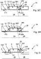
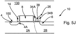
Figures 5A-5J show a method of making an LDMOS device of the kind shown inFigure 3 , according to an embodiment of this disclosure. - Embodiments of this disclosure are described in the following with reference to the accompanying drawings.
-
Figure 1 shows an example of a laterally-diffused metal-oxide semiconductor, "LDMOS",device 10. Thesemiconductor device 10 includes a semiconductor (e.g., silicon)substrate 2. Thesubstrate 2 has amajor surface 100. Thesemiconductor device 10 also includes agate 8 located on themajor surface 100. A gate dielectric 18 (e.g., an oxide) is located in between thegate 8 and themajor surface 100. The gate is provided withspacers spacers major surface 100. - The
semiconductor device 10 further includes asource region 4, which is located on a first side (the left-hand side of thegate 8 as viewed in the example ofFigure 1 ) of thegate 8. Thesource region 4 may include anextension region 4A located substantially beneath thespacer 14 on the first side of thegate 8. - The
semiconductor device 10 further includes a drain including adrain drift region 6, which is located on a second side of thegate 8 opposite the first side (the right-hand side of thegate 8 as viewed in the example ofFigure 1 ). - The breakdown voltage of a self-aligned
LDMOS device 10 of the kind shown inFigure 1 may generally be limited by thegate oxide 18 thickness of thesemiconductor device 10. -
Figure 2 shows a laterally-diffused metal-oxide, "LDMOS",device 10 according to an embodiment of this disclosure. - The
semiconductor device 10 includes a semiconductor (e.g., silicon)substrate 2. Thesubstrate 2 has amajor surface 100. Thesubstrate 2 has a firstdoped region 2A and a seconddoped region 2B. The firstdoped region 2A corresponds substantially to a gate channel region of thedevice 10, while the second doped region contains adrain drift region 6 of thedevice 10. The firstdoped region 2A may be doped to have a first conductivity type and the seconddoped region 2B may be doped to have a second conductivity type. In this embodiment, the first conductivity type is p-type, and the second conductivity type is n-type. - The
semiconductor device 10 also includes agate 8 located on themajor surface 100. In particular, thegate 8 may be located above the firstdoped region 2A. A gate dielectric 18 (e.g., an oxide) is located in between thegate 8 and themajor surface 100. Thegate 8 is provided withspacers first spacer 14 is located adjacent to a first sidewall of thegate 8 on a first side of the gate 8 (the left-hand side of thegate 8 as viewed in the example ofFigure 2 ). Thesecond spacer 26 is located adjacent to a second sidewall of thegate 8 on a second side of the gate 8 (the right-hand side of thegate 8 as viewed in the example ofFigure 2 ) opposite the first side of thegate 8. Dielectric may extend between thespacers gate 8, and between thespacers major surface 100. - The
semiconductor device 10 further includes asource region 4, which is located on the first side of thegate 8. Thesource region 4 may include anextension region 4A located substantially beneath thespacer 14 on the first side of thegate 8. Thesource region 4 and theextension region 4A may be doped regions having the second conductivity type (n-type, in this embodiment). - The
semiconductor device 10 further includes a drain including adrain drift region 6, which is located on the second side of thegate 8. Thedrain drift region 6 may be a doped region having the second conductivity type (n-type, in this embodiment). Thesource region 4, theextension region 4A and thedrain drift region 6 may be more highly doped than the seconddoped region 2B. - The
gate 8 may be covered with adielectric region 130. Thedielectric region 130 may include conductive interconnects for making electrical connections to thesource region 4, thedrain drift region 6 and thegate 8. Thedielectric region 130 may also cover thespacers source region 4 and thedrain drift region 6. - The
second spacer 26 is located between thegate 8 and thedrain drift 6 region when viewed from above themajor surface 100. - The
second spacer 26 has aproximal spacer portion 34A and adistal spacer portion 34B. Theproximal spacer portion 34A is proximal to thegate 8 and is located between thegate 8 and thedistal spacer portion 34B. Thedistal spacer portion 34B may be located between theproximal spacer portion 34A and thedrain drift region 6 when viewed from above themajor surface 100. As shown inFigure 2 , theproximal spacer portion 34A and thedistal spacer portion 34B define arecess 22. Therecess 22 is located in a center region of thesecond spacer 26. Therecess 22 may be filled with dielectric (e.g., oxide), for instance the dielectric of thedielectric region 130. - In the present embodiment, a lateral width (measured along the dimension of the channel region of the device 10) of the
second spacer 26 is greater than a lateral width of thefirst spacer 14 and smaller than twice the lateral width of thefirst spacer 14. As will be described below,proximal spacer portion 34A and thedistal spacer portion 34B of thesecond spacer 26 may each be formed using a similar or the same process as the process for forming thefirst spacer 14. In the present embodiment, theproximal spacer portion 34A adjoins thedistal spacer portion 34B at the center region of thesecond spacer 26. Therecess 22 may thus be formed at the point at which theproximal spacer portion 34A meets thedistal spacer portion 34B. -
Figure 3 shows a laterally-diffused metal-oxide, "LDMOS",device 10 according to another embodiment of this disclosure. Thedevice 10 in this embodiment is similar in some respects to the device shown inFigure 2 , and only the differences will be described here in detail. - The
gate 8 in this embodiment is again provided withspacers first spacer 14 is located adjacent to a first sidewall of thegate 8 on a first side of the gate 8 (the left-hand side of thegate 8 as viewed in the example ofFigure 3 ). As in the embodiment ofFigure 2 , thesecond spacer 26 is located adjacent to a second sidewall of thegate 8 on a second side of the gate 8 (the right-hand side of thegate 8 as viewed in the example ofFigure 3 ) opposite the first side of thegate 8. Again, dielectric may extend between thespacers gate 8, and between thespacers major surface 100. - The
second spacer 26 is again located between thegate 8 and thedrain drift 6 region when viewed from above themajor surface 100. Thesecond spacer 26 in this embodiment again has aproximal spacer portion 34A and adistal spacer portion 34B. Theproximal spacer portion 34A is proximal to thegate 8 and is located between thegate 8 and thedistal spacer portion 34B. Thedistal spacer portion 34B may be located between theproximal spacer portion 34A and thedrain drift region 6 when viewed from above themajor surface 100. - As shown in
Figure 3 , theproximal spacer portion 34A and thedistal spacer portion 34B define a recess. The recess is located in a center region of thesecond spacer 26. The recess may be at least partially filled with dielectric (e.g., oxide), for instance the dielectric of thedielectric region 130, thereby to form an oxide spacer part that overlies at least the center region of thesecond spacer 26. Note that in this embodiment, the recess forms a space orgap 38, which laterally separates theproximal spacer portion 34A from the distal spacer portion 34. Thespace 38 may be chosen to have a lateral width according to the desired overall lateral width of thesecond spacer 26. Note that in this embodiment, the lateral width of thesecond spacer 26 is greater than twice a lateral width of thefirst spacer 14. - As is known in the art, the vertical height (e.g., measured from the
major surface 100 of thesubstrate 2 inFigure 1 ) of spacers provided on the sidewalls of gates may taper (reduce) with increasing distance from the gate. Thefirst spacer 14 of the embodiments shown inFigures 2 and 3 may taper conventionally in this way. However, thesecond spacer 26 in the embodiments ofFigures 2 and 3 does not taper in this way, owing to the presence of therecess 22. - To form the
recess 22, theproximal spacer portion 34A may have a vertical height (e.g., measured from themajor surface 100 of thesubstrate 2 inFigures 2 and 3 ) which tapers (reduces) with increasing distance from thegate 8, while thedistal spacer portion 34B may have a vertical height (e.g., measured from themajor surface 100 of thesubstrate 2 inFigures 2 and 3 ) which tapers (reduces) with decreasing distance from thegate 8. Thus, the opposite directions of the tapering of theproximal spacer portion 34A and thedistal spacer portion 34B may form therecess 22 of thesecond spacer 26. In the embodiment ofFigure 2 , the vertical heights of theproximal spacer portion 34A and thedistal spacer portion 34B do not taper to zero, since theproximal spacer portion 34A adjoins thedistal spacer portion 34B. However, in the embodiment ofFigure 3 , the vertical heights of theproximal spacer portion 34A and thedistal spacer portion 34B may taper to zero or nearly zero, thereby to form the space orgap 38, which laterally separates theproximal spacer portion 34A from the distal spacer portion 34. -
Figures 4A-4F show a method of making anLDMOS device 10 of the kind shown inFigure 2 , according to an embodiment of this disclosure. - In a first stage, shown in
Figure 4A , a semiconductor (e.g., silicon)substrate 2 is provided. Thesubstrate 2 has amajor surface 100. Thesubstrate 2 has a firstdoped region 2A and a seconddoped region 2B, which may be formed using masking and ion implantation steps. The firstdoped region 2A corresponds substantially to a gate channel region of thedevice 10, while the second doped region contains adrain drift region 6 of thedevice 10. The firstdoped region 2A may be doped to have a first conductivity type and the seconddoped region 2B may be doped to have a second conductivity type. In this embodiment, the first conductivity type is p-type, and the second conductivity type is n-type. - In the first stage, the
gate 8 of thedevice 10 may be formed. This may involve depositing agate dielectric 112 on themajor surface 100 of thesubstrate 2 and then depositing a gate (electrode) material, such as polysilicon, onto thegate dielectric 112. As can be seen inFigure 4A , the formation of the gate may also involve forming asacrificial part 28, e.g., from the same material as thegate 8. Thegate 8 andsacrificial part 28 may be formed using a number of mask and etch steps. For instance, following the deposition of the gate material on themajor surface 100, amask 110 may be formed on the gate material. Themask 110 may have openings through which the gate material may be etched away, thereby arriving at the arrangement shown inFigure 4A . The mask may be patterned such that, after etching the gate material, thegate 8 is located above the firstdoped region 2A and thesacrificial part 28 is located on the second side of thegate 8, above the seconddoped region 2B and laterally separated from the gate by a space. This space will subsequently be used to define thesecond spacer 26. The lateral width of the space between thegate 28 and thesacrificial part 28 may thus be chosen according to the desired lateral width of thesecond spacer 26. In the present embodiment, the lateral width of the space between thegate 28 and thesacrificial part 28 is chosen to be greater than a lateral width of thefirst spacer 14 and smaller than twice the lateral width of thefirst spacer 14, to be formed subsequently. After the etching of the gate material, themask 110 may be removed. - In a next stage, shown in
Figure 4B , thefirst spacer 14 and thesecond spacer 26 are formed. Prior to the deposition of the spacer material, dielectric may be grown on the sidewalls of thegate 8 and thesacrificial part 28. The spacer material may then be deposited over the gate and thesacrificial part 28. Note that the spacer material substantially fills the space between thegate 8 and thesacrificial part 28. The spacer material may then be etched back. In one embodiment, the etching of the spacer material may be performed with an anisotropic etch. In terms of thefirst spacer 14, the etching back may conventionally form a tapered spacer. However, for thesecond spacer 26, the etching back of the spacer material leads to the formation of theproximal spacer portion 34A which tapers from the edge of thegate 8 and the formation of thedistal spacer portion 34B, which tapers from the edge of the sacrificial part 29. This leads to the formation of therecess 22. - In a next stage, shown in
Figure 4C , a maskingmaterial 170 such as photoresist is deposited and patterned such that an edge of the maskingmaterial 170 falls between thegate 8 and thesacrificial part 28. Prior to the deposition of the maskingmaterial 170, adielectric layer 120 may be formed over thegate 8, thespacers sacrificial part 28. - In a next stage, shown in
Figure 4D , thesacrificial part 28 may be removed by etching. Note that the maskingmaterial 170 may protect thegate 8 form etching during this stage. The masing material may then be removed. Further etching may be used to remove the dielectric 120 and the parts of the gate dielectric which are not located beneath thegate 8 andspacers - In a next stage, shown in
Figure 4E , thesource region 4,extension region 4A and draindrift region 6 may be formed e.g., using ion implantation followed by an anneal to activate the dopants. Thespacer 14 defines the edge of thesource region 4 closest to thegate 8 in a self-aligned manner. Similarly, thespacer 26 defines the edge of thedrain drift region 6 closest to thegate 8 in a self-aligned manner. Note that, because the lateral width of thesecond spacer 26 is greater than the lateral width of a conventional spacer (e.g., spacer 14) the edge of thedrain drift region 6 may be located further away from thegate 8. This may allow thedevice 10 to have a relatively high breakdown voltage. - In a next stage, shown in
Figure 4F , thedielectric region 130 may be deposited and patterned. Thedielectric region 130 may include conductive interconnects for making electrical connections to thesource region 4, thedrain drift region 6 and thegate 8. Note that thedielectric region 130 may substantially fill therecess 22. -
Figures 5A-5J show a method of making anLDMOS device 10 of the kind shown inFigure 3 , according to an embodiment of this disclosure. - This stage of the method may be substantially as described above in relation to
Figure 4A . However, unlike inFigure 4A , in the present embodiment, the lateral width of the space between thegate 28 and thesacrificial part 28 is chosen to be greater than twice a lateral width of thefirst spacer 14, to be formed subsequently. - In a next stage, shown in
Figure 5B , thefirst spacer 14 and thesecond spacer 26 are formed. Prior to the deposition of the spacer material, dielectric may be grown on the sidewalls of thegate 8 and thesacrificial part 28. The spacer material may then be deposited over the gate and thesacrificial part 28. Note that the spacer material substantially fills the space between thegate 8 and thesacrificial part 28. The gate material may then be etched back. In terms of thefirst spacer 14, the etching back may conventionally form a tapered spacer. - However, for the
second spacer 26, the etching back of the spacer material leads to the formation of theproximal spacer portion 34A which tapers from the edge of thegate 8 and the formation of thedistal spacer portion 34B, which tapers from the edge of the sacrificial part 29. Moreover, because the lateral width of the space between thegate 28 and thesacrificial part 28 is chosen to be greater than twice a lateral width of thefirst spacer 14, the vertical height of both theproximal spacer portion 34A and thedistal spacer portion 34B may reduce to zero (or near zero) such that therecess 22 between theproximal spacer portion 34A and thedistal spacer portion 34B takes the form of the space orgap 38 described above in relation toFigure 3 . Thespace 38 may be chosen to have a lateral width according to the desired overall lateral width of thesecond spacer 26, and this may be determined by the lateral spacing between thegate 8 and thesacrificial part 28. - In a next stage, shown in
Figure 5C , dielectric 140 (e.g., Tetraethyl orthosilicate (TEOS)), may be deposited over the arrangement shown inFigure 5B . Prior to the deposition of the dielectric 140, adielectric layer 114 may be formed over thegate 8, thespacers sacrificial part 28. This may protect, for example, thegate 8 during the etching described below in relation toFigure 5E . - In a next stage, shown in
Figure 5D , the dielectric 140 may be etched back to formfurther spacer parts - The
further spacer part 150 may cover thefirst spacer 14 and may taper downwardly from the edge of thegate 8, although at a slower tapering rate than thefirst spacer 14, such thefurther spacer part 150 extends further from thegate 8 than thefirst spacer 14. - The
further spacer part 160 may substantially fill the space orgap 38 and may cover theproximal spacer portion 34A and thedistal spacer portion 34B. As with thefurther spacer part 150, thefurther spacer part 160 may taper away from thegate 8 and thesacrificial part 28 at a slower rate than theproximal spacer portion 34A and thedistal spacer portion 34B. Note that a recess may be located in thefurther spacer part 160, similar to therecess 22 in thesecond spacer 22. - In a next stage, shown in
Figure 5E , a maskingmaterial 152 such as photoresist may be deposited and patterned such that an edge of the maskingmaterial 152 falls above thegate 8. Thefurther spacer part 150 may then be removed by etching. After thefurther spacer part 150 has been etched away, the maskingmaterial 152 may be removed (thedielectric layer 114 may also be removed), leading to the arrangement shown inFigure 5F . - In a next stage, shown in
Figure 5G , a maskingmaterial 170 such as photoresist is deposited and patterned such that an edge of the maskingmaterial 170 falls between thegate 8 and thesacrificial part 28. Prior to the deposition of the maskingmaterial 170, adielectric layer 180 may be formed over thegate 8, thespacers sacrificial part 28. - In a next stage, shown in
Figure 5H , thesacrificial part 28 may be removed by etching. Note that the maskingmaterial 170 may protect thegate 8 form etching during this stage. The maskingmaterial 170 may then be removed. Further etching may be used to remove the dielectric 180 and the parts of thegate dielectric 112 which are not located beneath thegate 8 andspacers - In a next stage, shown in
Figure 5I , thesource region 4,extension region 4A and draindrift region 6 may be formed e.g., using ion implantation followed by an anneal to activate the dopants. Thespacer 14 defines the edge of thesource region 4 closest to thegate 8 in a self-aligned manner. Similarly, thespacer 26 defines the edge of thedrain drift region 6 closest to thegate 8 in a self-aligned manner. Note that, because the lateral width of thesecond spacer 26 may be chosen as described above, the edge of thedrain drift region 6 may be located further away from thegate 8, when compared to a conventional spacer. This may allow thedevice 10 to have a relatively high breakdown voltage. In contrast to the embodiment ofFigures 2 and4 , the present embodiment may allow for a greater spacing between thedrain drift region 6 and thegate 8. - In a next stage, shown in
Figure 5J , thedielectric region 130 may be deposited and patterned. Thedielectric region 130 may include conductive interconnects for making electrical connections to thesource region 4, thedrain drift region 6 and thegate 8. Note that thedielectric region 130 in this embodiment may sit above thefurther spacer part 160. In this way, the material filling thespace 38 may be chosen to be different to the material of thedielectric region 130. - Accordingly, there has been described a laterally-diffused metal-oxide semiconductor, "LDMOS", device and a method of making the same. The device includes a gate located on a major surface of a semiconductor die, a source region located in the die on a first side of the gate, a drain drift region located in the die on a second side of the gate opposite the first side, a first spacer located adjacent to a first sidewall of the gate on the first side of the gate, and a second spacer located adjacent to a second sidewall of the gate on the second side of the gate. The second spacer is located between the gate and the drain drift region. The second spacer comprises a proximal spacer portion and a distal spacer portion. The proximal spacer portion is located between the gate and the distal spacer portion. The proximal spacer portion and the distal spacer portion define a recess.
- Although particular embodiments of this disclosure have been described, it will be appreciated that many modifications/additions and/or substitutions may be made within the scope of the claims.
Claims (15)
- A method of making a laterally-diffused metal-oxide semiconductor, "LDMOS", device, the method comprising:providing a semiconductor die having a major surface;forming a gate on the maj or surface of the semiconductor die;forming a first spacer located adjacent to a first sidewall of the gate on a first side of the gate;forming a second spacer located adjacent to a second sidewall of the gate on a second side of the gate opposite said first side of the gate;forming a source region located in the semiconductor die on said first side of the gate; andforming a drain drift region located in the semiconductor die on said second side of the gate,wherein the second spacer is located between the gate and the drain drift region when viewed from above said major surface of the semiconductor die, wherein the second spacer comprises a proximal spacer portion and a distal spacer portion, wherein the proximal spacer portion is located between the gate and the distal spacer portion, and wherein the proximal spacer portion and the distal spacer portion define a recess located in a center region of the second spacer.
- The method of claim 1, wherein:forming the gate includes forming a sacrificial gate portion laterally separated from the gate on the second side of the gate; andforming the second spacer comprises forming the proximal spacer portion adjacent to the second sidewall of the gate and forming the distal spacer portion adjacent to a sidewall of the sacrificial gate portion facing the second sidewall of the gate.
- The method of claim 2, further comprising removing the sacrificial gate portion after forming the second spacer.
- The method of claim 3, comprising:depositing a mask on the gate, the first spacer and at least part of the second spacer; andremoving the sacrificial gate portion by etching.
- The method of claim 3 or 4, comprising forming the drain drift region after removal of the sacrificial gate portion.
- The method of any one of claims 2 to 5, wherein the sacrificial gate portion is laterally separated from the gate by a distance that is greater than a lateral width of the first spacer and smaller than twice the lateral width of the first spacer, and wherein the proximal spacer portion adjoins the distal spacer portion at the center region of the second spacer.
- The method of any one of claims 2 to 5, wherein the sacrificial gate portion is laterally separated from the gate by a distance that is greater than twice a lateral width of the first spacer, and wherein the proximal spacer portion is laterally separated from the distal spacer portion.
- The method of claim 7, further comprising:depositing an oxide layer over the gate, the sacrificial gate portion, the first spacer and the second spacer; andetching the oxide layer back, to form:a first oxide spacer part that overlies at least part of the first spacer; anda second oxide spacer part that overlies at least the center region of the second spacer.
- The method of claim 8, wherein the second oxide spacer part at least partially fills a space located between the proximal spacer portion and the distal spacer portion.
- The method of claim 9, further comprising:masking the second spacer; andremoving the first oxide spacer part from the first spacer.
- The method of any preceding claim, further comprising depositing a layer of dielectric to completely cover the gate, the first spacer and the second spacer.
- A laterally-diffused metal-oxide semiconductor, "LDMOS", device comprising:a gate located on a major surface of a semiconductor die;a source region located in the semiconductor die on a first side of the gatea drain drift region located in the semiconductor die on a second side of the gate opposite said first side of the gate;a first spacer located adjacent to a first sidewall of the gate on said first side of the gate; anda second spacer located adjacent to a second sidewall of the gate on said second side of the gate,wherein the second spacer is located between the gate and the drain drift region when viewed from above said major surface of the semiconductor die, wherein the second spacer comprises a proximal spacer portion and a distal spacer portion, wherein the proximal spacer portion is located between the gate and the distal spacer portion, and wherein the proximal spacer portion and the distal spacer portion define a recess located in a center region of the second spacer.
- The LDMOS device of claim 12, wherein a lateral width of the second spacer is greater than a lateral width of the first spacer and smaller than twice the lateral width of the first spacer, and wherein the proximal spacer portion adjoins the distal spacer portion at the center region of the second spacer.
- The LDMOS device of claim 12, wherein a lateral width of the second spacer is greater than twice a lateral width of the first spacer, and wherein the proximal spacer portion is laterally separated from the distal spacer portion.
- The LDMOS device of claim 14, comprising an oxide spacer part that overlies at least the center region of the second spacer.
Applications Claiming Priority (1)
| Application Number | Priority Date | Filing Date | Title |
|---|---|---|---|
| US17/237,389 US20220344506A1 (en) | 2021-04-22 | 2021-04-22 | Semiconductor device and method of making a semiconductor device |
Publications (1)
| Publication Number | Publication Date |
|---|---|
| EP4080583A1 true EP4080583A1 (en) | 2022-10-26 |
Family
ID=80738927
Family Applications (1)
| Application Number | Title | Priority Date | Filing Date |
|---|---|---|---|
| EP22161830.9A Pending EP4080583A1 (en) | 2021-04-22 | 2022-03-14 | Semiconductor device and method of making a semiconductor device |
Country Status (3)
| Country | Link |
|---|---|
| US (1) | US20220344506A1 (en) |
| EP (1) | EP4080583A1 (en) |
| CN (1) | CN115241068A (en) |
Citations (3)
| Publication number | Priority date | Publication date | Assignee | Title |
|---|---|---|---|---|
| US20090261426A1 (en) * | 2008-04-17 | 2009-10-22 | International Business Machines Corporation | Lateral diffusion field effect transistor with drain region self-aligned to gate electrode |
| WO2012066695A1 (en) * | 2010-11-18 | 2012-05-24 | パナソニック株式会社 | Semiconductor device and method for manufacturing same |
| US20170077250A1 (en) * | 2015-09-15 | 2017-03-16 | United Microelectronics Corp. | High-voltage metal-oxide-semiconductor transistor device and manufacturing method thereof |
-
2021
- 2021-04-22 US US17/237,389 patent/US20220344506A1/en not_active Abandoned
-
2022
- 2022-03-14 EP EP22161830.9A patent/EP4080583A1/en active Pending
- 2022-04-22 CN CN202210430382.6A patent/CN115241068A/en active Pending
Patent Citations (3)
| Publication number | Priority date | Publication date | Assignee | Title |
|---|---|---|---|---|
| US20090261426A1 (en) * | 2008-04-17 | 2009-10-22 | International Business Machines Corporation | Lateral diffusion field effect transistor with drain region self-aligned to gate electrode |
| WO2012066695A1 (en) * | 2010-11-18 | 2012-05-24 | パナソニック株式会社 | Semiconductor device and method for manufacturing same |
| US20170077250A1 (en) * | 2015-09-15 | 2017-03-16 | United Microelectronics Corp. | High-voltage metal-oxide-semiconductor transistor device and manufacturing method thereof |
Also Published As
| Publication number | Publication date |
|---|---|
| CN115241068A (en) | 2022-10-25 |
| US20220344506A1 (en) | 2022-10-27 |
Similar Documents
| Publication | Publication Date | Title |
|---|---|---|
| EP3745467B1 (en) | Super-junction power semiconductor device and method of manufacture | |
| US10777661B2 (en) | Method of manufacturing shielded gate trench MOSFET devices | |
| CN100365826C (en) | Trench Power Metal Oxide Semiconductor Gate Devices | |
| JP5111744B2 (en) | Metal oxide semiconductor device with enhanced shielding structure | |
| US20040232481A1 (en) | Structure and method for forming a trench MOSFET having self-aligned features | |
| US20090085107A1 (en) | Trench MOSFET with thick bottom oxide tub | |
| US20110233659A1 (en) | Semiconductor power device and manufacturing method thereof | |
| CN113519054B (en) | Method of manufacturing a shielded gate trench MOSFET device | |
| US10840331B2 (en) | Semiconductor device | |
| KR20190037148A (en) | Semiconductor structure and associated fabricating method | |
| JP2005503023A (en) | Trench gate semiconductor device and its manufacture | |
| CN114446791B (en) | Method for manufacturing power semiconductor device with split gate structure | |
| US9991378B2 (en) | Trench power semiconductor device | |
| US8017494B2 (en) | Termination trench structure for mosgated device and process for its manufacture | |
| CN102593002A (en) | Vertical transistor manufacturing method and vertical transistor | |
| US6977413B2 (en) | Bar-type field effect transistor and method for the production thereof | |
| US20250089311A1 (en) | High voltage mosfet using shallow-shallow trench isolation structure | |
| CN114078956A (en) | Transistor device with buried field electrode connection | |
| WO2007072405A2 (en) | Semiconductor device with recessed field plate and method of manufacturing the same | |
| WO2001069685A2 (en) | Trench-gate semiconductor devices | |
| US20220344506A1 (en) | Semiconductor device and method of making a semiconductor device | |
| US11949009B2 (en) | Semiconductor die and method of manufacturing the same | |
| CN116741824A (en) | Semiconductor components and methods of forming the same | |
| US20060046389A1 (en) | Manufacturing process and structure of integrated circuit | |
| US20260122933A1 (en) | Method for manufacturing a trench schottky diode with adjustable forward voltage |
Legal Events
| Date | Code | Title | Description |
|---|---|---|---|
| PUAI | Public reference made under article 153(3) epc to a published international application that has entered the european phase |
Free format text: ORIGINAL CODE: 0009012 |
|
| STAA | Information on the status of an ep patent application or granted ep patent |
Free format text: STATUS: THE APPLICATION HAS BEEN PUBLISHED |
|
| AK | Designated contracting states |
Kind code of ref document: A1 Designated state(s): AL AT BE BG CH CY CZ DE DK EE ES FI FR GB GR HR HU IE IS IT LI LT LU LV MC MK MT NL NO PL PT RO RS SE SI SK SM TR |
|
| STAA | Information on the status of an ep patent application or granted ep patent |
Free format text: STATUS: REQUEST FOR EXAMINATION WAS MADE |
|
| 17P | Request for examination filed |
Effective date: 20230426 |
|
| RBV | Designated contracting states (corrected) |
Designated state(s): AL AT BE BG CH CY CZ DE DK EE ES FI FR GB GR HR HU IE IS IT LI LT LU LV MC MK MT NL NO PL PT RO RS SE SI SK SM TR |