EP4079711A1 - Copper/ceramic joined body and insulated circuit board - Google Patents
Copper/ceramic joined body and insulated circuit board Download PDFInfo
- Publication number
- EP4079711A1 EP4079711A1 EP20902360.5A EP20902360A EP4079711A1 EP 4079711 A1 EP4079711 A1 EP 4079711A1 EP 20902360 A EP20902360 A EP 20902360A EP 4079711 A1 EP4079711 A1 EP 4079711A1
- Authority
- EP
- European Patent Office
- Prior art keywords
- copper
- ceramic
- active metal
- bonded
- present
- Prior art date
- Legal status (The legal status is an assumption and is not a legal conclusion. Google has not performed a legal analysis and makes no representation as to the accuracy of the status listed.)
- Granted
Links
Images




Classifications
-
- H—ELECTRICITY
- H05—ELECTRIC TECHNIQUES NOT OTHERWISE PROVIDED FOR
- H05K—PRINTED CIRCUITS; CASINGS OR CONSTRUCTIONAL DETAILS OF ELECTRIC APPARATUS; MANUFACTURE OF ASSEMBLAGES OF ELECTRICAL COMPONENTS
- H05K1/00—Printed circuits
- H05K1/02—Details
- H05K1/09—Use of materials for the conductive, e.g. metallic pattern
-
- C—CHEMISTRY; METALLURGY
- C04—CEMENTS; CONCRETE; ARTIFICIAL STONE; CERAMICS; REFRACTORIES
- C04B—LIME, MAGNESIA; SLAG; CEMENTS; COMPOSITIONS THEREOF, e.g. MORTARS, CONCRETE OR LIKE BUILDING MATERIALS; ARTIFICIAL STONE; CERAMICS; REFRACTORIES; TREATMENT OF NATURAL STONE
- C04B37/00—Joining burned ceramic articles with other burned ceramic articles or other articles by heating
- C04B37/02—Joining burned ceramic articles with other burned ceramic articles or other articles by heating with metallic articles
- C04B37/023—Joining burned ceramic articles with other burned ceramic articles or other articles by heating with metallic articles characterised by the interlayer used
- C04B37/026—Joining burned ceramic articles with other burned ceramic articles or other articles by heating with metallic articles characterised by the interlayer used consisting of metals or metal salts
-
- B—PERFORMING OPERATIONS; TRANSPORTING
- B23—MACHINE TOOLS; METAL-WORKING NOT OTHERWISE PROVIDED FOR
- B23K—SOLDERING OR UNSOLDERING; WELDING; CLADDING OR PLATING BY SOLDERING OR WELDING; CUTTING BY APPLYING HEAT LOCALLY, e.g. FLAME CUTTING; WORKING BY LASER BEAM
- B23K1/00—Soldering, e.g. brazing, or unsoldering
- B23K1/0008—Soldering, e.g. brazing, or unsoldering specially adapted for particular articles or work
- B23K1/0016—Soldering of electronic components
-
- B—PERFORMING OPERATIONS; TRANSPORTING
- B23—MACHINE TOOLS; METAL-WORKING NOT OTHERWISE PROVIDED FOR
- B23K—SOLDERING OR UNSOLDERING; WELDING; CLADDING OR PLATING BY SOLDERING OR WELDING; CUTTING BY APPLYING HEAT LOCALLY, e.g. FLAME CUTTING; WORKING BY LASER BEAM
- B23K1/00—Soldering, e.g. brazing, or unsoldering
- B23K1/008—Soldering within a furnace
-
- B—PERFORMING OPERATIONS; TRANSPORTING
- B23—MACHINE TOOLS; METAL-WORKING NOT OTHERWISE PROVIDED FOR
- B23K—SOLDERING OR UNSOLDERING; WELDING; CLADDING OR PLATING BY SOLDERING OR WELDING; CUTTING BY APPLYING HEAT LOCALLY, e.g. FLAME CUTTING; WORKING BY LASER BEAM
- B23K1/00—Soldering, e.g. brazing, or unsoldering
- B23K1/19—Soldering, e.g. brazing, or unsoldering taking account of the properties of the materials to be soldered
-
- B—PERFORMING OPERATIONS; TRANSPORTING
- B23—MACHINE TOOLS; METAL-WORKING NOT OTHERWISE PROVIDED FOR
- B23K—SOLDERING OR UNSOLDERING; WELDING; CLADDING OR PLATING BY SOLDERING OR WELDING; CUTTING BY APPLYING HEAT LOCALLY, e.g. FLAME CUTTING; WORKING BY LASER BEAM
- B23K20/00—Non-electric welding by applying impact or other pressure, with or without the application of heat, e.g. cladding or plating
- B23K20/02—Non-electric welding by applying impact or other pressure, with or without the application of heat, e.g. cladding or plating by means of a press ; Diffusion bonding
- B23K20/023—Thermo-compression bonding
- B23K20/026—Thermo-compression bonding with diffusion of soldering material
-
- B—PERFORMING OPERATIONS; TRANSPORTING
- B23—MACHINE TOOLS; METAL-WORKING NOT OTHERWISE PROVIDED FOR
- B23K—SOLDERING OR UNSOLDERING; WELDING; CLADDING OR PLATING BY SOLDERING OR WELDING; CUTTING BY APPLYING HEAT LOCALLY, e.g. FLAME CUTTING; WORKING BY LASER BEAM
- B23K20/00—Non-electric welding by applying impact or other pressure, with or without the application of heat, e.g. cladding or plating
- B23K20/16—Non-electric welding by applying impact or other pressure, with or without the application of heat, e.g. cladding or plating with interposition of special material to facilitate connection of the parts, e.g. material for absorbing or producing gas
-
- B—PERFORMING OPERATIONS; TRANSPORTING
- B23—MACHINE TOOLS; METAL-WORKING NOT OTHERWISE PROVIDED FOR
- B23K—SOLDERING OR UNSOLDERING; WELDING; CLADDING OR PLATING BY SOLDERING OR WELDING; CUTTING BY APPLYING HEAT LOCALLY, e.g. FLAME CUTTING; WORKING BY LASER BEAM
- B23K20/00—Non-electric welding by applying impact or other pressure, with or without the application of heat, e.g. cladding or plating
- B23K20/22—Non-electric welding by applying impact or other pressure, with or without the application of heat, e.g. cladding or plating taking account of the properties of the materials to be welded
- B23K20/233—Non-electric welding by applying impact or other pressure, with or without the application of heat, e.g. cladding or plating taking account of the properties of the materials to be welded without ferrous layer
-
- B—PERFORMING OPERATIONS; TRANSPORTING
- B32—LAYERED PRODUCTS
- B32B—LAYERED PRODUCTS, i.e. PRODUCTS BUILT-UP OF STRATA OF FLAT OR NON-FLAT, e.g. CELLULAR OR HONEYCOMB, FORM
- B32B15/00—Layered products comprising a layer of metal
-
- H—ELECTRICITY
- H05—ELECTRIC TECHNIQUES NOT OTHERWISE PROVIDED FOR
- H05K—PRINTED CIRCUITS; CASINGS OR CONSTRUCTIONAL DETAILS OF ELECTRIC APPARATUS; MANUFACTURE OF ASSEMBLAGES OF ELECTRICAL COMPONENTS
- H05K1/00—Printed circuits
- H05K1/02—Details
- H05K1/0201—Thermal arrangements, e.g. for cooling, heating or preventing overheating
- H05K1/0203—Cooling of mounted components
- H05K1/0209—External configuration of printed circuit board adapted for heat dissipation, e.g. lay-out of conductors, coatings
-
- H—ELECTRICITY
- H05—ELECTRIC TECHNIQUES NOT OTHERWISE PROVIDED FOR
- H05K—PRINTED CIRCUITS; CASINGS OR CONSTRUCTIONAL DETAILS OF ELECTRIC APPARATUS; MANUFACTURE OF ASSEMBLAGES OF ELECTRICAL COMPONENTS
- H05K1/00—Printed circuits
- H05K1/02—Details
- H05K1/03—Use of materials for the substrate
- H05K1/0306—Inorganic insulating substrates, e.g. ceramic, glass
-
- H—ELECTRICITY
- H05—ELECTRIC TECHNIQUES NOT OTHERWISE PROVIDED FOR
- H05K—PRINTED CIRCUITS; CASINGS OR CONSTRUCTIONAL DETAILS OF ELECTRIC APPARATUS; MANUFACTURE OF ASSEMBLAGES OF ELECTRICAL COMPONENTS
- H05K1/00—Printed circuits
- H05K1/18—Printed circuits structurally associated with non-printed electric components
- H05K1/181—Printed circuits structurally associated with non-printed electric components associated with surface mounted components
-
- H—ELECTRICITY
- H05—ELECTRIC TECHNIQUES NOT OTHERWISE PROVIDED FOR
- H05K—PRINTED CIRCUITS; CASINGS OR CONSTRUCTIONAL DETAILS OF ELECTRIC APPARATUS; MANUFACTURE OF ASSEMBLAGES OF ELECTRICAL COMPONENTS
- H05K3/00—Apparatus or processes for manufacturing printed circuits
- H05K3/38—Improvement of the adhesion between the insulating substrate and the metal
-
- H—ELECTRICITY
- H05—ELECTRIC TECHNIQUES NOT OTHERWISE PROVIDED FOR
- H05K—PRINTED CIRCUITS; CASINGS OR CONSTRUCTIONAL DETAILS OF ELECTRIC APPARATUS; MANUFACTURE OF ASSEMBLAGES OF ELECTRICAL COMPONENTS
- H05K3/00—Apparatus or processes for manufacturing printed circuits
- H05K3/38—Improvement of the adhesion between the insulating substrate and the metal
- H05K3/388—Improvement of the adhesion between the insulating substrate and the metal by the use of a metallic or inorganic thin film adhesion layer
-
- H—ELECTRICITY
- H10—SEMICONDUCTOR DEVICES; ELECTRIC SOLID-STATE DEVICES NOT OTHERWISE PROVIDED FOR
- H10W—GENERIC PACKAGES, INTERCONNECTIONS, CONNECTORS OR OTHER CONSTRUCTIONAL DETAILS OF DEVICES COVERED BY CLASS H10
- H10W70/00—Package substrates; Interposers; Redistribution layers [RDL]
- H10W70/60—Insulating or insulated package substrates; Interposers; Redistribution layers
- H10W70/67—Insulating or insulated package substrates; Interposers; Redistribution layers characterised by their insulating layers or insulating parts
- H10W70/68—Shapes or dispositions thereof
-
- B—PERFORMING OPERATIONS; TRANSPORTING
- B23—MACHINE TOOLS; METAL-WORKING NOT OTHERWISE PROVIDED FOR
- B23K—SOLDERING OR UNSOLDERING; WELDING; CLADDING OR PLATING BY SOLDERING OR WELDING; CUTTING BY APPLYING HEAT LOCALLY, e.g. FLAME CUTTING; WORKING BY LASER BEAM
- B23K2101/00—Articles made by soldering, welding or cutting
- B23K2101/36—Electric or electronic devices
- B23K2101/40—Semiconductor devices
-
- B—PERFORMING OPERATIONS; TRANSPORTING
- B23—MACHINE TOOLS; METAL-WORKING NOT OTHERWISE PROVIDED FOR
- B23K—SOLDERING OR UNSOLDERING; WELDING; CLADDING OR PLATING BY SOLDERING OR WELDING; CUTTING BY APPLYING HEAT LOCALLY, e.g. FLAME CUTTING; WORKING BY LASER BEAM
- B23K2101/00—Articles made by soldering, welding or cutting
- B23K2101/36—Electric or electronic devices
- B23K2101/42—Printed circuits
-
- B—PERFORMING OPERATIONS; TRANSPORTING
- B23—MACHINE TOOLS; METAL-WORKING NOT OTHERWISE PROVIDED FOR
- B23K—SOLDERING OR UNSOLDERING; WELDING; CLADDING OR PLATING BY SOLDERING OR WELDING; CUTTING BY APPLYING HEAT LOCALLY, e.g. FLAME CUTTING; WORKING BY LASER BEAM
- B23K2103/00—Materials to be soldered, welded or cut
- B23K2103/08—Non-ferrous metals or alloys
- B23K2103/12—Copper or alloys thereof
-
- B—PERFORMING OPERATIONS; TRANSPORTING
- B23—MACHINE TOOLS; METAL-WORKING NOT OTHERWISE PROVIDED FOR
- B23K—SOLDERING OR UNSOLDERING; WELDING; CLADDING OR PLATING BY SOLDERING OR WELDING; CUTTING BY APPLYING HEAT LOCALLY, e.g. FLAME CUTTING; WORKING BY LASER BEAM
- B23K2103/00—Materials to be soldered, welded or cut
- B23K2103/18—Dissimilar materials
-
- B—PERFORMING OPERATIONS; TRANSPORTING
- B23—MACHINE TOOLS; METAL-WORKING NOT OTHERWISE PROVIDED FOR
- B23K—SOLDERING OR UNSOLDERING; WELDING; CLADDING OR PLATING BY SOLDERING OR WELDING; CUTTING BY APPLYING HEAT LOCALLY, e.g. FLAME CUTTING; WORKING BY LASER BEAM
- B23K2103/00—Materials to be soldered, welded or cut
- B23K2103/50—Inorganic materials other than metals or composite materials
- B23K2103/52—Ceramics
-
- C—CHEMISTRY; METALLURGY
- C04—CEMENTS; CONCRETE; ARTIFICIAL STONE; CERAMICS; REFRACTORIES
- C04B—LIME, MAGNESIA; SLAG; CEMENTS; COMPOSITIONS THEREOF, e.g. MORTARS, CONCRETE OR LIKE BUILDING MATERIALS; ARTIFICIAL STONE; CERAMICS; REFRACTORIES; TREATMENT OF NATURAL STONE
- C04B2235/00—Aspects relating to ceramic starting mixtures or sintered ceramic products
- C04B2235/65—Aspects relating to heat treatments of ceramic bodies such as green ceramics or pre-sintered ceramics, e.g. burning, sintering or melting processes
- C04B2235/658—Atmosphere during thermal treatment
- C04B2235/6581—Total pressure below 1 atmosphere, e.g. vacuum
-
- C—CHEMISTRY; METALLURGY
- C04—CEMENTS; CONCRETE; ARTIFICIAL STONE; CERAMICS; REFRACTORIES
- C04B—LIME, MAGNESIA; SLAG; CEMENTS; COMPOSITIONS THEREOF, e.g. MORTARS, CONCRETE OR LIKE BUILDING MATERIALS; ARTIFICIAL STONE; CERAMICS; REFRACTORIES; TREATMENT OF NATURAL STONE
- C04B2235/00—Aspects relating to ceramic starting mixtures or sintered ceramic products
- C04B2235/70—Aspects relating to sintered or melt-casted ceramic products
- C04B2235/96—Properties of ceramic products, e.g. mechanical properties such as strength, toughness, wear resistance
-
- C—CHEMISTRY; METALLURGY
- C04—CEMENTS; CONCRETE; ARTIFICIAL STONE; CERAMICS; REFRACTORIES
- C04B—LIME, MAGNESIA; SLAG; CEMENTS; COMPOSITIONS THEREOF, e.g. MORTARS, CONCRETE OR LIKE BUILDING MATERIALS; ARTIFICIAL STONE; CERAMICS; REFRACTORIES; TREATMENT OF NATURAL STONE
- C04B2237/00—Aspects relating to ceramic laminates or to joining of ceramic articles with other articles by heating
- C04B2237/02—Aspects relating to interlayers, e.g. used to join ceramic articles with other articles by heating
- C04B2237/04—Ceramic interlayers
- C04B2237/08—Non-oxidic interlayers
-
- C—CHEMISTRY; METALLURGY
- C04—CEMENTS; CONCRETE; ARTIFICIAL STONE; CERAMICS; REFRACTORIES
- C04B—LIME, MAGNESIA; SLAG; CEMENTS; COMPOSITIONS THEREOF, e.g. MORTARS, CONCRETE OR LIKE BUILDING MATERIALS; ARTIFICIAL STONE; CERAMICS; REFRACTORIES; TREATMENT OF NATURAL STONE
- C04B2237/00—Aspects relating to ceramic laminates or to joining of ceramic articles with other articles by heating
- C04B2237/02—Aspects relating to interlayers, e.g. used to join ceramic articles with other articles by heating
- C04B2237/12—Metallic interlayers
- C04B2237/122—Metallic interlayers based on refractory metals
-
- C—CHEMISTRY; METALLURGY
- C04—CEMENTS; CONCRETE; ARTIFICIAL STONE; CERAMICS; REFRACTORIES
- C04B—LIME, MAGNESIA; SLAG; CEMENTS; COMPOSITIONS THEREOF, e.g. MORTARS, CONCRETE OR LIKE BUILDING MATERIALS; ARTIFICIAL STONE; CERAMICS; REFRACTORIES; TREATMENT OF NATURAL STONE
- C04B2237/00—Aspects relating to ceramic laminates or to joining of ceramic articles with other articles by heating
- C04B2237/02—Aspects relating to interlayers, e.g. used to join ceramic articles with other articles by heating
- C04B2237/12—Metallic interlayers
- C04B2237/123—Metallic interlayers based on iron group metals, e.g. steel
-
- C—CHEMISTRY; METALLURGY
- C04—CEMENTS; CONCRETE; ARTIFICIAL STONE; CERAMICS; REFRACTORIES
- C04B—LIME, MAGNESIA; SLAG; CEMENTS; COMPOSITIONS THEREOF, e.g. MORTARS, CONCRETE OR LIKE BUILDING MATERIALS; ARTIFICIAL STONE; CERAMICS; REFRACTORIES; TREATMENT OF NATURAL STONE
- C04B2237/00—Aspects relating to ceramic laminates or to joining of ceramic articles with other articles by heating
- C04B2237/02—Aspects relating to interlayers, e.g. used to join ceramic articles with other articles by heating
- C04B2237/12—Metallic interlayers
- C04B2237/125—Metallic interlayers based on noble metals, e.g. silver
-
- C—CHEMISTRY; METALLURGY
- C04—CEMENTS; CONCRETE; ARTIFICIAL STONE; CERAMICS; REFRACTORIES
- C04B—LIME, MAGNESIA; SLAG; CEMENTS; COMPOSITIONS THEREOF, e.g. MORTARS, CONCRETE OR LIKE BUILDING MATERIALS; ARTIFICIAL STONE; CERAMICS; REFRACTORIES; TREATMENT OF NATURAL STONE
- C04B2237/00—Aspects relating to ceramic laminates or to joining of ceramic articles with other articles by heating
- C04B2237/02—Aspects relating to interlayers, e.g. used to join ceramic articles with other articles by heating
- C04B2237/12—Metallic interlayers
- C04B2237/126—Metallic interlayers wherein the active component for bonding is not the largest fraction of the interlayer
- C04B2237/128—The active component for bonding being silicon
-
- C—CHEMISTRY; METALLURGY
- C04—CEMENTS; CONCRETE; ARTIFICIAL STONE; CERAMICS; REFRACTORIES
- C04B—LIME, MAGNESIA; SLAG; CEMENTS; COMPOSITIONS THEREOF, e.g. MORTARS, CONCRETE OR LIKE BUILDING MATERIALS; ARTIFICIAL STONE; CERAMICS; REFRACTORIES; TREATMENT OF NATURAL STONE
- C04B2237/00—Aspects relating to ceramic laminates or to joining of ceramic articles with other articles by heating
- C04B2237/30—Composition of layers of ceramic laminates or of ceramic or metallic articles to be joined by heating, e.g. Si substrates
- C04B2237/32—Ceramic
- C04B2237/36—Non-oxidic
- C04B2237/368—Silicon nitride
-
- C—CHEMISTRY; METALLURGY
- C04—CEMENTS; CONCRETE; ARTIFICIAL STONE; CERAMICS; REFRACTORIES
- C04B—LIME, MAGNESIA; SLAG; CEMENTS; COMPOSITIONS THEREOF, e.g. MORTARS, CONCRETE OR LIKE BUILDING MATERIALS; ARTIFICIAL STONE; CERAMICS; REFRACTORIES; TREATMENT OF NATURAL STONE
- C04B2237/00—Aspects relating to ceramic laminates or to joining of ceramic articles with other articles by heating
- C04B2237/30—Composition of layers of ceramic laminates or of ceramic or metallic articles to be joined by heating, e.g. Si substrates
- C04B2237/40—Metallic
- C04B2237/407—Copper
-
- C—CHEMISTRY; METALLURGY
- C04—CEMENTS; CONCRETE; ARTIFICIAL STONE; CERAMICS; REFRACTORIES
- C04B—LIME, MAGNESIA; SLAG; CEMENTS; COMPOSITIONS THEREOF, e.g. MORTARS, CONCRETE OR LIKE BUILDING MATERIALS; ARTIFICIAL STONE; CERAMICS; REFRACTORIES; TREATMENT OF NATURAL STONE
- C04B2237/00—Aspects relating to ceramic laminates or to joining of ceramic articles with other articles by heating
- C04B2237/50—Processing aspects relating to ceramic laminates or to the joining of ceramic articles with other articles by heating
- C04B2237/60—Forming at the joining interface or in the joining layer specific reaction phases or zones, e.g. diffusion of reactive species from the interlayer to the substrate or from a substrate to the joining interface, carbide forming at the joining interface
-
- C—CHEMISTRY; METALLURGY
- C04—CEMENTS; CONCRETE; ARTIFICIAL STONE; CERAMICS; REFRACTORIES
- C04B—LIME, MAGNESIA; SLAG; CEMENTS; COMPOSITIONS THEREOF, e.g. MORTARS, CONCRETE OR LIKE BUILDING MATERIALS; ARTIFICIAL STONE; CERAMICS; REFRACTORIES; TREATMENT OF NATURAL STONE
- C04B2237/00—Aspects relating to ceramic laminates or to joining of ceramic articles with other articles by heating
- C04B2237/50—Processing aspects relating to ceramic laminates or to the joining of ceramic articles with other articles by heating
- C04B2237/70—Forming laminates or joined articles comprising layers of a specific, unusual thickness
- C04B2237/704—Forming laminates or joined articles comprising layers of a specific, unusual thickness of one or more of the ceramic layers or articles
-
- C—CHEMISTRY; METALLURGY
- C04—CEMENTS; CONCRETE; ARTIFICIAL STONE; CERAMICS; REFRACTORIES
- C04B—LIME, MAGNESIA; SLAG; CEMENTS; COMPOSITIONS THEREOF, e.g. MORTARS, CONCRETE OR LIKE BUILDING MATERIALS; ARTIFICIAL STONE; CERAMICS; REFRACTORIES; TREATMENT OF NATURAL STONE
- C04B2237/00—Aspects relating to ceramic laminates or to joining of ceramic articles with other articles by heating
- C04B2237/50—Processing aspects relating to ceramic laminates or to the joining of ceramic articles with other articles by heating
- C04B2237/70—Forming laminates or joined articles comprising layers of a specific, unusual thickness
- C04B2237/706—Forming laminates or joined articles comprising layers of a specific, unusual thickness of one or more of the metallic layers or articles
-
- C—CHEMISTRY; METALLURGY
- C04—CEMENTS; CONCRETE; ARTIFICIAL STONE; CERAMICS; REFRACTORIES
- C04B—LIME, MAGNESIA; SLAG; CEMENTS; COMPOSITIONS THEREOF, e.g. MORTARS, CONCRETE OR LIKE BUILDING MATERIALS; ARTIFICIAL STONE; CERAMICS; REFRACTORIES; TREATMENT OF NATURAL STONE
- C04B35/00—Shaped ceramic products characterised by their composition; Ceramics compositions; Processing powders of inorganic compounds preparatory to the manufacturing of ceramic products
- C04B35/622—Forming processes; Processing powders of inorganic compounds preparatory to the manufacturing of ceramic products
- C04B35/64—Burning or sintering processes
- C04B35/645—Pressure sintering
-
- H—ELECTRICITY
- H05—ELECTRIC TECHNIQUES NOT OTHERWISE PROVIDED FOR
- H05K—PRINTED CIRCUITS; CASINGS OR CONSTRUCTIONAL DETAILS OF ELECTRIC APPARATUS; MANUFACTURE OF ASSEMBLAGES OF ELECTRICAL COMPONENTS
- H05K2201/00—Indexing scheme relating to printed circuits covered by H05K1/00
- H05K2201/01—Dielectrics
- H05K2201/0137—Materials
- H05K2201/0175—Inorganic, non-metallic layer, e.g. resist or dielectric for printed capacitor
-
- H—ELECTRICITY
- H05—ELECTRIC TECHNIQUES NOT OTHERWISE PROVIDED FOR
- H05K—PRINTED CIRCUITS; CASINGS OR CONSTRUCTIONAL DETAILS OF ELECTRIC APPARATUS; MANUFACTURE OF ASSEMBLAGES OF ELECTRICAL COMPONENTS
- H05K2201/00—Indexing scheme relating to printed circuits covered by H05K1/00
- H05K2201/06—Thermal details
- H05K2201/066—Heatsink mounted on the surface of the printed circuit board [PCB]
-
- H—ELECTRICITY
- H10—SEMICONDUCTOR DEVICES; ELECTRIC SOLID-STATE DEVICES NOT OTHERWISE PROVIDED FOR
- H10W—GENERIC PACKAGES, INTERCONNECTIONS, CONNECTORS OR OTHER CONSTRUCTIONAL DETAILS OF DEVICES COVERED BY CLASS H10
- H10W40/00—Arrangements for thermal protection or thermal control
- H10W40/20—Arrangements for cooling
- H10W40/25—Arrangements for cooling characterised by their materials
- H10W40/255—Arrangements for cooling characterised by their materials having a laminate or multilayered structure, e.g. direct bond copper [DBC] ceramic substrates
Definitions
- the present invention relates to a copper/ceramic bonded body in which a copper member made of copper or a copper alloy and a ceramic member made of silicon-containing ceramics are bonded to each other, and an insulating circuit substrate in which a copper sheet made of copper or a copper alloy is bonded to a surface of a ceramic substrate made of silicon-containing ceramics.
- a power module, an LED module, and a thermoelectric module have a structure in which a power semiconductor element, an LED element, and a thermoelectric element are bonded to an insulating circuit substrate in which a circuit layer made of a conductive material is formed on one surface of an insulating layer.
- a power semiconductor element for high-power control used for controlling a wind power generation, an electric vehicle, a hybrid vehicle, or the like has a large amount of heat generated during operation. Therefore, as a substrate on which the power semiconductor element is mounted, an insulating circuit substrate including a ceramic substrate and a circuit layer formed by bonding a metal plate having excellent conductivity to one surface of the ceramic substrate has been widely used in the related art. As the insulating circuit substrate, one having a metal layer formed by bonding a metal plate to the other surface of the ceramic substrate is also provided.
- Patent Document 1 proposes a power module substrate in which a first metal plate and the second metal plate constituting a circuit layer and a metal layer are made of a copper sheet, and the copper sheet is directly bonded to a ceramic substrate by a DBC method.
- the copper sheet and the ceramic substrate are bonded to each other by forming a liquid phase at an interface between the copper sheet and the ceramic substrate by using a eutectic reaction of copper with a copper oxide.
- Patent Document 2 proposes an insulating circuit substrate in which a circuit layer and a metal layer are formed by bonding a copper sheet to one surface and the other surface of a ceramic substrate.
- the copper sheet is disposed on one surface and the other surface of the ceramic substrate with an Ag-Cu-Ti-based brazing material interposed therebetween, and the copper sheet is bonded thereto by performing a heating treatment (so-called active metal brazing method).
- active metal brazing method since the brazing material containing Ti is used as an active metal, the wettability between the molten brazing material and the ceramic substrate is improved, and the ceramic substrate and the copper sheet are satisfactorily bonded to each other.
- Patent Document 3 proposes a power module substrate in which a copper sheet made of copper or a copper alloy and a ceramic substrate made of silicon nitride are bonded to each other using a bonding material containing Ag and Ti, and in which a nitride compound layer and an Ag-Cu eutectic layer are formed at a bonded interface, and a thickness of the nitride compound layer is in a range of 0.15 ⁇ m or more and 1.0 ⁇ m or less.
- the bonding temperature needs to be set to 1065°C or higher (equal to or higher than eutectic point temperature of copper and copper oxide), so that there is a concern that the ceramic substrate deteriorates during bonding.
- a bonding temperature is set to a relatively high temperature of at 900°C, so that there is a problem that the ceramic substrate deteriorates.
- Patent Document 3 since the copper sheet made of copper or a copper alloy and the ceramic substrate made of silicon nitride are bonded to each other by using the bonding material containing Ag and Ti, the ceramic member and the copper member can be bonded to each other at a relatively low temperature condition, and deterioration of the ceramic member during bonding can be suppressed.
- the present invention has been made in view of the above-described circumstances, and an objective of the present invention is to provide a copper/ceramic bonded body and an insulating circuit substrate, which have a high brazing bonding strength and particularly excellent reliability of a thermal cycle (ceramic substrate is less likely to break).
- a copper/ceramic bonded body includes: a copper member made of copper or a copper alloy; and a ceramic member made of silicon-containing ceramics, the copper member and the ceramic member being bonded to each other, in which a maximum indentation hardness in a region is set to be in a range of 70 mgf/ ⁇ m 2 or more and 150 mgf/ ⁇ m 2 or less, the region being from 10 ⁇ m to 50 ⁇ m with reference to a bonded interface between the copper member and the ceramic member toward the copper member side.
- the maximum indentation hardness in the region from 10 ⁇ m to 50 ⁇ m from the bonded interface between the copper member and the ceramic member to the copper member side is set to 70 mgf/ ⁇ m 2 or more, the copper in the vicinity of the bonded interface is sufficiently melted, to form a liquid phase, and the ceramic member and the copper member are firmly bonded to each other.
- the maximum indentation hardness in the above-described region is suppressed to 150 mgf/ ⁇ m 2 or less, the vicinity of the bonded interface is not harder than necessary, and the generation of cracks during loading of the thermal cycle can be suppressed.
- an active metal compound layer containing a compound of one or more active metals selected from the group consisting of Ti, Zr, Nb, and Hf is formed on a ceramic member side, and that the maximum particle size of the active metal compound particles in the active metal compound layer is 180 nm or less.
- a proportion of a grain boundary region (metal phase) having a relatively low hardness in the active metal compound layer increases, and the impact resistance of the active metal compound layer is improved.
- a terminal material is ultrasonically bonded to the copper member, it is possible to suppress the generation of cracks in the active metal compound layer, and to suppress peeling of the copper member from the ceramic member and the generation of cracks in the ceramic member.
- the copper/ceramic bonded body according to the present invention it is preferable that Si, Cu, and Ag are present in the active metal compound layer.
- An insulating circuit substrate includes: a copper sheet made of copper or a copper alloy; and a ceramic substrate made of silicon-containing ceramics, the copper sheet being bonded to a surface of the ceramic substrate, in which a maximum indentation hardness in a region is set to be in a range of 70 mgf/ ⁇ m 2 or more and 150 mgf/ ⁇ m 2 or less, the region being from 10 ⁇ m to 50 ⁇ m with reference to a bonded interface between the copper sheet and the ceramic substrate toward the copper sheet side.
- the maximum indentation hardness in the region from 10 ⁇ m to 50 ⁇ m from the bonded interface between the copper sheet and the ceramic substrate to the copper sheet side is set to 70 mgf/ ⁇ m 2 or more, the copper in the vicinity of the bonded interface is sufficiently melted, to form a liquid phase, and the ceramic substrate and the copper sheet are firmly bonded to each other.
- the maximum indentation hardness in the above-described region is suppressed to 150 mgf/ ⁇ m 2 or less, the vicinity of the bonded interface is not harder than necessary, and the generation of cracks during loading of the thermal cycle can be suppressed.
- an active metal compound layer containing a compound of one or more active metals selected from the group consisting of Ti, Zr, Nb, and Hf is formed on a ceramic substrate side, and that the maximum particle size of the active metal compound particles in the active metal compound layer is 180 nm or less.
- a proportion of a grain boundary region (metal phase) having a relatively low hardness in the active metal compound layer increases, and impact resistance of the active metal compound layer is improved.
- a terminal material is ultrasonically bonded to the copper sheet, it is possible to suppress the generation of cracks in the active metal compound layer, and to suppress peeling of the copper sheet from the ceramic substrate and the generation of cracks in the ceramic substrate.
- the active metal compound layer it is preferable that Si, Cu, and Ag are present in the active metal compound layer.
- a copper/ceramic bonded body and an insulating circuit substrate which have a high brazing bonding strength and particularly excellent reliability of a thermal cycle.
- a copper/ceramic bonded body according to the present embodiment is an insulating circuit substrate 10 formed by bonding a ceramic substrate 11 as a ceramic member made of ceramics to a copper sheet 22 (circuit layer 12) and a copper sheet 23 (metal layer 13) as a copper member made of copper or a copper alloy.
- Fig. 1 shows a power module 1 including the insulating circuit substrate 10 according to the present embodiment.
- the power module 1 includes the insulating circuit substrate 10 on which the circuit layer 12 and the metal layer 13 are disposed, a semiconductor element 3 bonded to one surface (upper surface in Fig. 1 ) of the circuit layer 12 with a bonding layer 2 interposed therebetween, and a heat sink 30 disposed on the other side (lower side in Fig. 1 ) of the metal layer 13.
- the semiconductor element 3 is made of a semiconductor material such as Si.
- the semiconductor element 3 and the circuit layer 12 are bonded to each other with the bonding layer 2 interposed therebetween.
- the bonding layer 2 is made of, for example, a Sn-Ag-based, Sn-In-based, or Sn-Ag-Cu-based solder material.
- the heat sink 30 dissipates heat from the above-mentioned insulating circuit substrate 10.
- the heat sink 30 is made of copper or a copper alloy, and in the present embodiment, the heat sink 30 is made of phosphorus deoxidized copper.
- the heat sink 30 is provided with a passage 31 through which a cooling fluid flows.
- the heat sink 30 and the metal layer 13 are bonded to each other by a solder layer 32 made of a solder material.
- the solder layer 32 is made of, for example, a Sn-Ag-based, Sn-In-based, or Sn-Ag-Cu-based solder material.
- the insulating circuit substrate 10 includes the ceramic substrate 11, the circuit layer 12 disposed on one surface (upper surface in Fig. 1 ) of the ceramic substrate 11, and the metal layer 13 disposed on the other surface (lower surface in Fig. 1 ) of the ceramic substrate 11.
- the ceramic substrate 11 is made of silicon-containing ceramics having excellent insulating properties and heat radiation, and in the present embodiment, the ceramic substrate 11 is made of silicon nitride (Si 3 N 4 ).
- the thickness of the ceramic substrate 11 is set to be in a range of, for example, 0.2 mm or more and 1.5 mm or less, and in the present embodiment, the thickness is set to 0.32 mm.
- the circuit layer 12 is formed by bonding the copper sheet 22 made of copper or a copper alloy to one surface (upper surface in Fig. 6 ) of the ceramic substrate 11.
- the circuit layer 12 is formed by bonding the copper sheet 22 made of a rolled plate of oxygen-free copper to the ceramic substrate 11.
- the thickness of the copper sheet 22 serving as the circuit layer 12 is set to be in a range of 0.1 mm or more and 2.0 mm or less, and in the present embodiment, the thickness is set to 0.6 mm.
- the metal layer 13 is formed by bonding the copper sheet 23 made of copper or a copper alloy to the other surface (lower surface in Fig. 6 ) of the ceramic substrate 11.
- the metal layer 13 is formed by bonding the copper sheet 23 made of a rolled plate of oxygen-free copper to the ceramic substrate 11.
- the thickness of the copper sheet 23 serving as the metal layer 13 is set to be in a range of 0.1 mm or more and 2.0 mm or less, and in the present embodiment, the thickness is set to 0.6 mm.
- an active metal compound layer 41 containing a compound of one or more active metals selected from the group consisting of Ti, Zr, Nb, and Hf is formed.
- the active metal compound layer 41 is formed by reacting an active metal contained in a bonding material with the ceramic substrate 11.
- Ti is used as the active metal and the ceramic substrate 11 is made of aluminum nitride, so that the active metal compound layer 41 becomes a titanium nitride (TiN) layer.
- TiN titanium nitride
- the maximum indentation hardness in a region from 10 ⁇ m to 50 ⁇ m from the bonded interface between the circuit layer 12 (metal layer 13) and the ceramic substrate 11 to the circuit layer 12 (metal layer 13) side is in a range of 70 mgf/ ⁇ m 2 or more and 150 mgf/ ⁇ m 2 or less.
- the lower limit of the maximum indentation hardness is preferably 75 mgf/ ⁇ m 2 or more, and more preferably 85 mgf/ ⁇ m 2 or more.
- the upper limit of the maximum indentation hardness is preferably 135 mgf/ ⁇ m 2 or less, and more preferably 125 mgf/ ⁇ m 2 or less.
- the maximum particle size of active metal compound particles 45 in the active metal compound layer 41 is 180 nm or less. Grain boundaries between the active metal compound particles 45 form a metal phase. Since the maximum particle size of the active metal compound particles 45 is 180 nm or less, a proportion of a metal phase having a relatively low hardness increases, and impact resistance of the active metal compound layer 41 is improved. As a result, for example, when a terminal material is ultrasonically bonded to the copper member, it is possible to suppress the generation of cracks in the active metal compound layer 41, and to suppress peeling of the copper member from the ceramic member and the generation of cracks in the ceramic member.
- the maximum particle size of the active metal compound particles 45 in the active metal compound layer 41 is more preferably 150 nm or less, and still more preferably 120 nm or less.
- the active metal compound layer 41 it is preferable that Si, Cu, and Ag are present in the active metal compound layer 41.
- Si, Cu, and Ag present in the active metal compound layer 41 can be confirmed by observing the interparticles and the grain boundaries of the active metal compound particles 45 in the active metal compound layer 41 using a transmission electron microscope and obtaining an EDS spectrum.
- An example of the EDS spectrum of the active metal compound layer 41 is shown in Fig. 4 . Peaks of Si, Cu, and Ag are confirmed, and it can be seen that Si, Cu, and Ag are present in the active metal compound layer 41.
- the ceramic substrate 11 made of silicon nitride (Si 3 N 4 ) is prepared, and as shown in Fig. 6 , an Ag-Ti-based brazing material (Ag-Cu-Ti-based brazing material) 24 is disposed between the copper sheet 22 serving as the circuit layer 12 and the ceramic substrate 11, and between the copper sheet 23 serving as the metal layer 13 and the ceramic substrate 11.
- Ag-Ti-based brazing material Ag-Cu-Ti-based brazing material
- the Ag-Ti-based brazing material (Ag-Cu-Ti-based brazing material) 24 for example, it is preferable to use a composition containing Cu in a range of 0 mass% or more and 32 mass% or less, Ti as an active metal in a range of 0.5 mass% or more and 20 mass% or less, and a balance being Ag and inevitable impurities.
- the thickness of the Ag-Cu-Ti-based brazing material 24 is preferably in a range of 2 ⁇ m or more and 10 ⁇ m or less.
- the copper sheet 22 and the ceramic substrate 11 are heated in a heating furnace in a vacuum atmosphere in a state of being pressed, to melt the Ag-Ti-based brazing material (Ag-Cu-Ti-based brazing material) 24.
- a heating temperature in the heating step S02 is in a range of the eutectic point temperature of Cu and Si or more and 850°C or less.
- a temperature integration value at the above-described heating temperature is in a range of 1 °C ⁇ h or higher and 110 °C ⁇ h or lower.
- a pressing load in the heating step S02 is in a range of 0.029 MPa or more and 2.94 MPa or less.
- the molten Ag-Ti-based brazing material (Ag-Cu-Ti-based brazing material) 24 is solidified by cooling.
- a cooling rate in the cooling step S03 is preferably in a range of 2 °C/min or higher and 10 °C/min or lower.
- a eutectic liquid phase is present at the grain boundary of TiN in the active metal compound layer 41, and Si on the ceramic substrate 11 side and Ag, Cu, and Ti of the Ag-Cu-Ti-based brazing material 24 diffuse into each other by using the eutectic liquid phase as a diffusion path, thereby promoting the interfacial reaction of the ceramic substrate 11.
- the maximum indentation hardness in a region from 10 ⁇ m to 50 ⁇ m from the bonded interface with the ceramic substrate 11 to the circuit layer 12 (metal layer 13) side is in a range of 70 mgf/ ⁇ m 2 or more and 150 mgf/ ⁇ m 2 or less.
- the ceramic substrate 11 and the copper sheets 22 and 23 are bonded to each other by the laminating step S01, the heating step S02, and the cooling step S03, thereby producing the insulating circuit substrate 10 according to the present embodiment.
- the heat sink 30 is bonded to the other surface side of the metal layer 13 of the insulating circuit substrate 10.
- the insulating circuit substrate 10 and the heat sink 30 are laminated with a solder material interposed therebetween and are loaded into a heating furnace such that the insulating circuit substrate 10 and the heat sink 30 are solder-bonded to each other with the solder layer 32 interposed therebetween.
- the semiconductor element 3 is bonded to one surface of the circuit layer 12 of the insulating circuit substrate 10 by soldering.
- the power module 1 shown in Fig. 1 is produced by the above steps.
- the insulating circuit substrate 10 (copper/ceramic bonded body) according to the present embodiment having the above configuration, since the maximum indentation hardness in the region from 10 ⁇ m to 50 ⁇ m from the bonded interface between the circuit layer 12 (metal layer 13) and the ceramic substrate 11 to the circuit layer 12 (metal layer 13) is set to 70 mgf/ ⁇ m 2 or more, the copper in the vicinity of the bonded interface is sufficiently melted to form a liquid phase, and the ceramic substrate 11 and the circuit layer 12 (metal layer 13) are more firmly bonded to each other.
- the maximum indentation hardness is suppressed to 150 mgf/ ⁇ m 2 or less, the vicinity of the bonded interface is not harder than necessary, and the generation of cracks during loading of the thermal cycle can be suppressed.
- the maximum particle size of the active metal compound particles 45 in the active metal compound layer 41 formed at the bonded interface between the ceramic substrate 11 and the circuit layer 12 (metal layer 13) is 180 nm or less, a proportion of a grain boundary region formed of a metal phase having a relatively low hardness in the active metal compound layer 41 increases, and impact resistance of the active metal compound layer 41 can be secured.
- a terminal material is ultrasonically bonded to the circuit layer 12 (metal layer 13)
- the insulating circuit substrate 10 in a case where Si, Cu, and Ag are present in the active metal compound layer 41, it is possible to suppress the generation of cracks in the active metal compound layer 41, and to obtain an insulating circuit substrate 10 having a high brazing bonding strength because no unreacted portion is formed at the bonded interface between the ceramic substrate 11 and the circuit layer 12 (metal layer 13).
- the semiconductor element is mounted on the insulating circuit substrate to form the power module, but the present embodiment is not limited thereto.
- an LED element may be mounted on the circuit layer of the insulating circuit substrate to form an LED module, or a thermoelectric element may be mounted on the circuit layer of the insulating circuit substrate to form a thermoelectric module.
- the circuit layer and the metal layer are both made of a copper sheet made of copper or a copper alloy, but the present invention is not limited thereto.
- the circuit layer and the ceramic substrate are made of the copper/ceramic bonded body according to the present invention
- the material and the bonding method of the metal layer there is no limitation on the material and the bonding method of the metal layer.
- the metal layer may be made of aluminum or an aluminum alloy, or may be made of a laminate of copper and aluminum.
- the metal layer and the ceramic substrate are made of the copper/ceramic bonded body according to the present invention
- the material and the bonding method of the circuit layer there is no limitation on the material and the bonding method of the circuit layer.
- the circuit layer may be made of aluminum or an aluminum alloy, or may be made of a laminate of copper and aluminum.
- the Ag-Ti-based brazing material (Ag-Cu-Ti-based brazing material) 24 is disposed between the copper sheets 22 and 23 and the ceramic substrate 11 in the laminating step S01, but the present invention is not limited thereto, and a bonding material containing another active metal may be used.
- the ceramic substrate is made of silicon nitride (Si 3 N 4 ), but the present invention is not limited thereto, and the ceramic substrate may be made of other silicon-containing ceramics.
- a ceramic substrate 40 mm ⁇ 40 mm ⁇ 0.32 mm
- silicon nitride Si 3 N 4
- a copper sheet (37 mm ⁇ 37 mm ⁇ thickness of 1.0 mm) made of oxygen-free copper was bonded to both surfaces of the ceramic substrate under the conditions shown in Table 1 by using an Ag-Cu-based brazing material containing an active metal shown in Table 1, to obtain an insulating circuit substrate (copper/ceramic bonded body).
- the degree of vacuum of a vacuum furnace at the time of bonding was set to 5 ⁇ 10 -3 Pa.
- the maximum indentation hardness in the vicinity of a bonded interface, and the reliability of the thermal cycle were evaluated as follows.
- the maximum indentation hardness was measured in a region from 10 ⁇ m to 50 ⁇ m from the bonded interface between the copper sheet and the ceramic substrate to the copper sheet side by using an indentation hardness tester (ENT-1100a manufactured by Elionix Inc.).
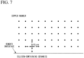
- a target section was exposed by buffing to make a measuring surface, and as shown in Fig. 7 , the indentation hardness was measured at 50 measurement points at intervals of 10 ⁇ m, and the maximum value of the indentation hardness among them was confirmed.
- a load applied in the indenter indentation process and an indentation depth can be continuously measured, and information such as plasticity/elasticity/creep can be obtained from a load-displacement curve.
- the bonded interface between the copper sheet and the ceramic substrate was inspected by SAT inspection, and the presence or absence of ceramic breaking was determined. ⁇ 78 ° C ⁇ 2 minutes ⁇ ⁇ 350 ° C ⁇ 2 minutes
- a ceramic substrate (40 mm ⁇ 40 mm ⁇ 0.32 mm) made of silicon nitride (Si 3 N 4 ) was prepared.
- a copper sheet (37 mm ⁇ 37 mm ⁇ thickness of 0.2 mm) made of oxygen-free copper was bonded to both surfaces of the ceramic substrate under the conditions shown in Table 2 by using an Ag-Cu-based brazing material containing an active metal shown in Table 2, to obtain an insulating circuit substrate (copper/ceramic bonded body).
- a degree of vacuum of a vacuum furnace at the time of bonding was set to 5 ⁇ 10 -3 Pa.
- the maximum indentation hardness in the vicinity of a bonded interface was evaluated by the same method as in Example 1.
- the maximum particle size of the active metal compound particles in the active metal compound layer was evaluated by the method shown below.
- the active metal compound layer was observed at a magnification of 500,000x by using a transmission electron microscope (Titan ChemiSTEM manufactured by FEI Company), to obtain a HAADF image.
- the grain boundaries in the active metal compound layer were integrated for 1100 frames at an acceleration voltage of 200 kV, a magnification of 500,000x to 700,000x, and 7 ⁇ s per point by using a transmission electron microscope (Titan ChemiSTEM manufactured by FEI Company). In the EDS spectrum, in a case where Si, Ag, and Cu were 0.15 cps/eV, Si, Ag, and Cu were evaluated as "present".
- a copper terminal (10 mm ⁇ 20 mm ⁇ 2.0 mm in thickness) was ultrasonically bonded to the insulating circuit substrate by using an ultrasonic metal bonding machine (60C-904 manufactured by Ultrasonic Engineering Co., Ltd.) under the conditions of a load of 850 N, a collapse amount of 0.7 mm, and a bonding area of 5 mm ⁇ 5 mm. Fifty copper terminals were bonded at a time.
- the bonded interface between the copper sheet and the ceramic substrate was inspected by using an ultrasonic flaw detector (FineSAT200 manufactured by Hitachi Solutions, Ltd.).
- a case where peeling of the copper sheet from the ceramic substrate or ceramic breaking was observed in 5 pieces or more out of 50 pieces was evaluated as "D”
- a case where peeling of the copper sheet from the ceramic substrate or ceramic breaking was observed in 3 pieces or more and 4 pieces or less out of 50 pieces was evaluated as "C”
- a case where peeling of the copper sheet from the ceramic substrate or ceramic breaking was observed in 1 piece or more and 2 pieces or less out of 50 pieces was evaluated as "B”
- a case where peeling of the copper sheet from the ceramic substrate or ceramic breaking was not observed in all 50 pieces was evaluated as "A”.
- the evaluation results are shown in Table 2.
Landscapes
- Engineering & Computer Science (AREA)
- Chemical & Material Sciences (AREA)
- Microelectronics & Electronic Packaging (AREA)
- Mechanical Engineering (AREA)
- Ceramic Engineering (AREA)
- Materials Engineering (AREA)
- Structural Engineering (AREA)
- Organic Chemistry (AREA)
- Manufacturing & Machinery (AREA)
- Inorganic Chemistry (AREA)
- Ceramic Products (AREA)
- Manufacturing Of Printed Wiring (AREA)
Abstract
Description
- The present invention relates to a copper/ceramic bonded body in which a copper member made of copper or a copper alloy and a ceramic member made of silicon-containing ceramics are bonded to each other, and an insulating circuit substrate in which a copper sheet made of copper or a copper alloy is bonded to a surface of a ceramic substrate made of silicon-containing ceramics.
- Priority is claimed on
Japanese Patent Application No. 2019-228780, filed December 19, 2019 Japanese Patent Application No. 2020-196300, filed November 26, 2020 - A power module, an LED module, and a thermoelectric module have a structure in which a power semiconductor element, an LED element, and a thermoelectric element are bonded to an insulating circuit substrate in which a circuit layer made of a conductive material is formed on one surface of an insulating layer.
- For example, a power semiconductor element for high-power control used for controlling a wind power generation, an electric vehicle, a hybrid vehicle, or the like has a large amount of heat generated during operation. Therefore, as a substrate on which the power semiconductor element is mounted, an insulating circuit substrate including a ceramic substrate and a circuit layer formed by bonding a metal plate having excellent conductivity to one surface of the ceramic substrate has been widely used in the related art. As the insulating circuit substrate, one having a metal layer formed by bonding a metal plate to the other surface of the ceramic substrate is also provided.
- For example, Patent Document 1 proposes a power module substrate in which a first metal plate and the second metal plate constituting a circuit layer and a metal layer are made of a copper sheet, and the copper sheet is directly bonded to a ceramic substrate by a DBC method. In this DBC method, the copper sheet and the ceramic substrate are bonded to each other by forming a liquid phase at an interface between the copper sheet and the ceramic substrate by using a eutectic reaction of copper with a copper oxide.
- In addition,
Patent Document 2 proposes an insulating circuit substrate in which a circuit layer and a metal layer are formed by bonding a copper sheet to one surface and the other surface of a ceramic substrate. In Patent Document 1, the copper sheet is disposed on one surface and the other surface of the ceramic substrate with an Ag-Cu-Ti-based brazing material interposed therebetween, and the copper sheet is bonded thereto by performing a heating treatment (so-called active metal brazing method). In the active metal brazing method, since the brazing material containing Ti is used as an active metal, the wettability between the molten brazing material and the ceramic substrate is improved, and the ceramic substrate and the copper sheet are satisfactorily bonded to each other. - Further,
Patent Document 3 proposes a power module substrate in which a copper sheet made of copper or a copper alloy and a ceramic substrate made of silicon nitride are bonded to each other using a bonding material containing Ag and Ti, and in which a nitride compound layer and an Ag-Cu eutectic layer are formed at a bonded interface, and a thickness of the nitride compound layer is in a range of 0.15 µm or more and 1.0 µm or less. -
- [Patent Document 1]
Japanese Unexamined Patent Application, First Publication No. H04-162756 - [Patent Document 2]
Japanese Patent No. 3211856 - [Patent Document 3]
Japanese Unexamined Patent Application, First Publication No. 2018-008869 - However, as disclosed in Patent Document 1, when the ceramic substrate and the copper sheet are bonded to each other by the DBC method, the bonding temperature needs to be set to 1065°C or higher (equal to or higher than eutectic point temperature of copper and copper oxide), so that there is a concern that the ceramic substrate deteriorates during bonding.
- In addition, as disclosed in
Patent Document 2, when the ceramic substrate and the copper sheet are bonded to each other by the active metal brazing method, a bonding temperature is set to a relatively high temperature of at 900°C, so that there is a problem that the ceramic substrate deteriorates. - Here, in
Patent Document 3, since the copper sheet made of copper or a copper alloy and the ceramic substrate made of silicon nitride are bonded to each other by using the bonding material containing Ag and Ti, the ceramic member and the copper member can be bonded to each other at a relatively low temperature condition, and deterioration of the ceramic member during bonding can be suppressed. - By the way, recently, depending on the application of the insulating circuit substrate, a thermal cycle that is more severe than in the related art is loaded.
- Therefore, there is a demand for an insulating circuit substrate that has a high brazing bonding strength and does not cause cracks in the ceramic substrate even during loading of a thermal cycle, even in an application where a thermal cycle that is more severe than in the related art is loaded.
- The present invention has been made in view of the above-described circumstances, and an objective of the present invention is to provide a copper/ceramic bonded body and an insulating circuit substrate, which have a high brazing bonding strength and particularly excellent reliability of a thermal cycle (ceramic substrate is less likely to break).
- In order to solve the above-described problem, a copper/ceramic bonded body according to the present invention includes: a copper member made of copper or a copper alloy; and a ceramic member made of silicon-containing ceramics, the copper member and the ceramic member being bonded to each other, in which a maximum indentation hardness in a region is set to be in a range of 70 mgf/µm2 or more and 150 mgf/µm2 or less, the region being from 10 µm to 50 µm with reference to a bonded interface between the copper member and the ceramic member toward the copper member side.
- According to the copper/ceramic bonded body according to the present invention, since the maximum indentation hardness in the region from 10 µm to 50 µm from the bonded interface between the copper member and the ceramic member to the copper member side is set to 70 mgf/µm2 or more, the copper in the vicinity of the bonded interface is sufficiently melted, to form a liquid phase, and the ceramic member and the copper member are firmly bonded to each other.
- On the other hand, since the maximum indentation hardness in the above-described region is suppressed to 150 mgf/µm2 or less, the vicinity of the bonded interface is not harder than necessary, and the generation of cracks during loading of the thermal cycle can be suppressed.
- Therefore, it is possible to provide a copper/ceramic bonded body having a high brazing bonding strength and particularly excellent reliability of a thermal cycle.
- Here, in the copper/ceramic bonded body according to the present invention, it is preferable that, at the bonded interface between the ceramic member and the copper member, an active metal compound layer containing a compound of one or more active metals selected from the group consisting of Ti, Zr, Nb, and Hf is formed on a ceramic member side, and that the maximum particle size of the active metal compound particles in the active metal compound layer is 180 nm or less.
- In this case, a proportion of a grain boundary region (metal phase) having a relatively low hardness in the active metal compound layer increases, and the impact resistance of the active metal compound layer is improved. As a result, for example, when a terminal material is ultrasonically bonded to the copper member, it is possible to suppress the generation of cracks in the active metal compound layer, and to suppress peeling of the copper member from the ceramic member and the generation of cracks in the ceramic member.
- In the copper/ceramic bonded body according to the present invention, it is preferable that Si, Cu, and Ag are present in the active metal compound layer.
- In this case, since Si, Cu, and Ag are present in the active metal compound layer, it is possible to suppress the generation of cracks in the active metal compound layer, and to obtain a copper/ceramic bonded body having a high brazing bonding strength because no unreacted portion is formed at the bonded interface between the copper member and the ceramic member.
- An insulating circuit substrate according to the present invention includes: a copper sheet made of copper or a copper alloy; and a ceramic substrate made of silicon-containing ceramics, the copper sheet being bonded to a surface of the ceramic substrate, in which a maximum indentation hardness in a region is set to be in a range of 70 mgf/µm2 or more and 150 mgf/µm2 or less, the region being from 10 µm to 50 µm with reference to a bonded interface between the copper sheet and the ceramic substrate toward the copper sheet side.
- According to the insulating circuit substrate according to the present invention, since the maximum indentation hardness in the region from 10 µm to 50 µm from the bonded interface between the copper sheet and the ceramic substrate to the copper sheet side is set to 70 mgf/µm2 or more, the copper in the vicinity of the bonded interface is sufficiently melted, to form a liquid phase, and the ceramic substrate and the copper sheet are firmly bonded to each other.
- On the other hand, since the maximum indentation hardness in the above-described region is suppressed to 150 mgf/µm2 or less, the vicinity of the bonded interface is not harder than necessary, and the generation of cracks during loading of the thermal cycle can be suppressed.
- Therefore, it is possible to provide an insulating circuit substrate having a high brazing bonding strength and particularly excellent reliability of a thermal cycle.
- Here, in the insulating circuit substrate according to the present invention, it is preferable that, at the bonded interface between the copper sheet and the ceramic substrate, an active metal compound layer containing a compound of one or more active metals selected from the group consisting of Ti, Zr, Nb, and Hf is formed on a ceramic substrate side, and that the maximum particle size of the active metal compound particles in the active metal compound layer is 180 nm or less.
- In this case, a proportion of a grain boundary region (metal phase) having a relatively low hardness in the active metal compound layer increases, and impact resistance of the active metal compound layer is improved. As a result, for example, when a terminal material is ultrasonically bonded to the copper sheet, it is possible to suppress the generation of cracks in the active metal compound layer, and to suppress peeling of the copper sheet from the ceramic substrate and the generation of cracks in the ceramic substrate.
- In the insulating circuit substrate according to the present invention, it is preferable that Si, Cu, and Ag are present in the active metal compound layer.
- In this case, since Si, Cu, and Ag are present in the active metal compound layer, it is possible to suppress the generation of cracks in the active metal compound layer, and to obtain an insulating circuit substrate having a high brazing bonding strength because no unreacted portion is formed at the bonded interface between the copper sheet and the ceramic substrate.
- According to the present invention, it is possible to provide a copper/ceramic bonded body and an insulating circuit substrate, which have a high brazing bonding strength and particularly excellent reliability of a thermal cycle.
-
-
Fig. 1 is a schematic explanatory view of a power module using an insulating circuit substrate according to an embodiment of the present invention. -
Fig. 2 is an enlarged explanatory view of a bonded interface between a circuit layer (metal layer) and a ceramic substrate of the insulating circuit substrate according to the embodiment of the present invention. -
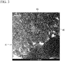
Fig. 3 is an observation photograph of an active metal compound layer formed at the bonded interface between the circuit layer (metal layer) and the ceramic substrate of the insulating circuit substrate according to the embodiment of the present invention. -
Fig. 4 is an example of an EDS spectrum of the active metal compound layer. -
Fig. 5 is a flowchart of a production method of the insulating circuit substrate according to the embodiment of the present invention. -
Fig. 6 is a schematic explanatory view of the production method of the insulating circuit substrate according to the embodiment of the present invention. -
Fig. 7 is an explanatory view showing a measurement point of the maximum indentation hardness in the vicinity of a bonded interface in Examples. -
Fig. 8 is an explanatory view showing a measurement principle of an indentation hardness test in Examples. - Hereinafter, an embodiment of the present invention will be described with reference to the accompanying drawings.
- A copper/ceramic bonded body according to the present embodiment is an
insulating circuit substrate 10 formed by bonding aceramic substrate 11 as a ceramic member made of ceramics to a copper sheet 22 (circuit layer 12) and a copper sheet 23 (metal layer 13) as a copper member made of copper or a copper alloy.Fig. 1 shows a power module 1 including theinsulating circuit substrate 10 according to the present embodiment. - The power module 1 includes the
insulating circuit substrate 10 on which thecircuit layer 12 and themetal layer 13 are disposed, asemiconductor element 3 bonded to one surface (upper surface inFig. 1 ) of thecircuit layer 12 with abonding layer 2 interposed therebetween, and aheat sink 30 disposed on the other side (lower side inFig. 1 ) of themetal layer 13. - The
semiconductor element 3 is made of a semiconductor material such as Si. Thesemiconductor element 3 and thecircuit layer 12 are bonded to each other with thebonding layer 2 interposed therebetween. - The
bonding layer 2 is made of, for example, a Sn-Ag-based, Sn-In-based, or Sn-Ag-Cu-based solder material. - The
heat sink 30 dissipates heat from the above-mentionedinsulating circuit substrate 10. Theheat sink 30 is made of copper or a copper alloy, and in the present embodiment, theheat sink 30 is made of phosphorus deoxidized copper. Theheat sink 30 is provided with apassage 31 through which a cooling fluid flows. - In the present embodiment, the
heat sink 30 and themetal layer 13 are bonded to each other by asolder layer 32 made of a solder material. Thesolder layer 32 is made of, for example, a Sn-Ag-based, Sn-In-based, or Sn-Ag-Cu-based solder material. - As shown in
Fig. 1 , the insulatingcircuit substrate 10 according to the present embodiment includes theceramic substrate 11, thecircuit layer 12 disposed on one surface (upper surface inFig. 1 ) of theceramic substrate 11, and themetal layer 13 disposed on the other surface (lower surface inFig. 1 ) of theceramic substrate 11. - The
ceramic substrate 11 is made of silicon-containing ceramics having excellent insulating properties and heat radiation, and in the present embodiment, theceramic substrate 11 is made of silicon nitride (Si3N4). The thickness of theceramic substrate 11 is set to be in a range of, for example, 0.2 mm or more and 1.5 mm or less, and in the present embodiment, the thickness is set to 0.32 mm. - As shown in
Fig. 6 , thecircuit layer 12 is formed by bonding thecopper sheet 22 made of copper or a copper alloy to one surface (upper surface inFig. 6 ) of theceramic substrate 11. - In the present embodiment, the
circuit layer 12 is formed by bonding thecopper sheet 22 made of a rolled plate of oxygen-free copper to theceramic substrate 11. - The thickness of the
copper sheet 22 serving as thecircuit layer 12 is set to be in a range of 0.1 mm or more and 2.0 mm or less, and in the present embodiment, the thickness is set to 0.6 mm. - As shown in
Fig. 6 , themetal layer 13 is formed by bonding thecopper sheet 23 made of copper or a copper alloy to the other surface (lower surface inFig. 6 ) of theceramic substrate 11. - In the present embodiment, the
metal layer 13 is formed by bonding thecopper sheet 23 made of a rolled plate of oxygen-free copper to theceramic substrate 11. - The thickness of the
copper sheet 23 serving as themetal layer 13 is set to be in a range of 0.1 mm or more and 2.0 mm or less, and in the present embodiment, the thickness is set to 0.6 mm. - At the bonded interface between the
ceramic substrate 11 and the circuit layer 12 (metal layer 13), as shown inFig. 2 , an activemetal compound layer 41 containing a compound of one or more active metals selected from the group consisting of Ti, Zr, Nb, and Hf is formed. - The active
metal compound layer 41 is formed by reacting an active metal contained in a bonding material with theceramic substrate 11. - In the present embodiment, Ti is used as the active metal and the
ceramic substrate 11 is made of aluminum nitride, so that the activemetal compound layer 41 becomes a titanium nitride (TiN) layer. - In the insulating
circuit substrate 10 according to the present embodiment, the maximum indentation hardness in a region from 10 µm to 50 µm from the bonded interface between the circuit layer 12 (metal layer 13) and theceramic substrate 11 to the circuit layer 12 (metal layer 13) side is in a range of 70 mgf/µm2 or more and 150 mgf/µm2 or less. - The lower limit of the maximum indentation hardness is preferably 75 mgf/µm2 or more, and more preferably 85 mgf/µm2 or more. On the other hand, the upper limit of the maximum indentation hardness is preferably 135 mgf/µm2 or less, and more preferably 125 mgf/µm2 or less.
- In the insulating
circuit substrate 10 according to the present embodiment, as shown inFig. 3 , it is preferable that the maximum particle size of activemetal compound particles 45 in the activemetal compound layer 41 is 180 nm or less. Grain boundaries between the activemetal compound particles 45 form a metal phase. Since the maximum particle size of the activemetal compound particles 45 is 180 nm or less, a proportion of a metal phase having a relatively low hardness increases, and impact resistance of the activemetal compound layer 41 is improved. As a result, for example, when a terminal material is ultrasonically bonded to the copper member, it is possible to suppress the generation of cracks in the activemetal compound layer 41, and to suppress peeling of the copper member from the ceramic member and the generation of cracks in the ceramic member. - The maximum particle size of the active
metal compound particles 45 in the activemetal compound layer 41 is more preferably 150 nm or less, and still more preferably 120 nm or less. - Further, in the insulating
circuit substrate 10 according to the present embodiment, it is preferable that Si, Cu, and Ag are present in the activemetal compound layer 41. - Si, Cu, and Ag present in the active
metal compound layer 41 can be confirmed by observing the interparticles and the grain boundaries of the activemetal compound particles 45 in the activemetal compound layer 41 using a transmission electron microscope and obtaining an EDS spectrum. An example of the EDS spectrum of the activemetal compound layer 41 is shown inFig. 4 . Peaks of Si, Cu, and Ag are confirmed, and it can be seen that Si, Cu, and Ag are present in the activemetal compound layer 41. - Hereinafter, a production method of the insulating
circuit substrate 10 according to the present embodiment will be described with reference toFigs. 5 and6 . - First, the
ceramic substrate 11 made of silicon nitride (Si3N4) is prepared, and as shown inFig. 6 , an Ag-Ti-based brazing material (Ag-Cu-Ti-based brazing material) 24 is disposed between thecopper sheet 22 serving as thecircuit layer 12 and theceramic substrate 11, and between thecopper sheet 23 serving as themetal layer 13 and theceramic substrate 11. - As the Ag-Ti-based brazing material (Ag-Cu-Ti-based brazing material) 24, for example, it is preferable to use a composition containing Cu in a range of 0 mass% or more and 32 mass% or less, Ti as an active metal in a range of 0.5 mass% or more and 20 mass% or less, and a balance being Ag and inevitable impurities. The thickness of the Ag-Cu-Ti-based
brazing material 24 is preferably in a range of 2 µm or more and 10 µm or less. - Next, the
copper sheet 22 and theceramic substrate 11 are heated in a heating furnace in a vacuum atmosphere in a state of being pressed, to melt the Ag-Ti-based brazing material (Ag-Cu-Ti-based brazing material) 24. - Here, a heating temperature in the heating step S02 is in a range of the eutectic point temperature of Cu and Si or more and 850°C or less. In the heating step S02, a temperature integration value at the above-described heating temperature is in a range of 1 °C·h or higher and 110 °C·h or lower.
- A pressing load in the heating step S02 is in a range of 0.029 MPa or more and 2.94 MPa or less.
- Then, after the heating step S02, the molten Ag-Ti-based brazing material (Ag-Cu-Ti-based brazing material) 24 is solidified by cooling.
- A cooling rate in the cooling step S03 is preferably in a range of 2 °C/min or higher and 10 °C/min or lower.
- Here, in the heating step S02, a eutectic liquid phase is present at the grain boundary of TiN in the active
metal compound layer 41, and Si on theceramic substrate 11 side and Ag, Cu, and Ti of the Ag-Cu-Ti-basedbrazing material 24 diffuse into each other by using the eutectic liquid phase as a diffusion path, thereby promoting the interfacial reaction of theceramic substrate 11. - As a result, the maximum indentation hardness in a region from 10 µm to 50 µm from the bonded interface with the
ceramic substrate 11 to the circuit layer 12 (metal layer 13) side is in a range of 70 mgf/µm2 or more and 150 mgf/µm2 or less. - As described above, the
ceramic substrate 11 and thecopper sheets circuit substrate 10 according to the present embodiment. - Next, the
heat sink 30 is bonded to the other surface side of themetal layer 13 of the insulatingcircuit substrate 10. - The insulating
circuit substrate 10 and theheat sink 30 are laminated with a solder material interposed therebetween and are loaded into a heating furnace such that the insulatingcircuit substrate 10 and theheat sink 30 are solder-bonded to each other with thesolder layer 32 interposed therebetween. - Next, the
semiconductor element 3 is bonded to one surface of thecircuit layer 12 of the insulatingcircuit substrate 10 by soldering. - The power module 1 shown in
Fig. 1 is produced by the above steps. - According to the insulating circuit substrate 10 (copper/ceramic bonded body) according to the present embodiment having the above configuration, since the maximum indentation hardness in the region from 10 µm to 50 µm from the bonded interface between the circuit layer 12 (metal layer 13) and the
ceramic substrate 11 to the circuit layer 12 (metal layer 13) is set to 70 mgf/µm2 or more, the copper in the vicinity of the bonded interface is sufficiently melted to form a liquid phase, and theceramic substrate 11 and the circuit layer 12 (metal layer 13) are more firmly bonded to each other. - On the other hand, since the maximum indentation hardness is suppressed to 150 mgf/µm2 or less, the vicinity of the bonded interface is not harder than necessary, and the generation of cracks during loading of the thermal cycle can be suppressed.
- In the insulating
circuit substrate 10 according to the present embodiment, in a case where the maximum particle size of the activemetal compound particles 45 in the activemetal compound layer 41 formed at the bonded interface between theceramic substrate 11 and the circuit layer 12 (metal layer 13) is 180 nm or less, a proportion of a grain boundary region formed of a metal phase having a relatively low hardness in the activemetal compound layer 41 increases, and impact resistance of the activemetal compound layer 41 can be secured. As a result, for example, when a terminal material is ultrasonically bonded to the circuit layer 12 (metal layer 13), it is possible to suppress the generation of cracks in the activemetal compound layer 41, and to suppress peeling of the circuit layer 12 (metal layer 13) from theceramic substrate 11 and the generation of cracks in theceramic substrate 11. - In the insulating
circuit substrate 10 according to the present embodiment, in a case where Si, Cu, and Ag are present in the activemetal compound layer 41, it is possible to suppress the generation of cracks in the activemetal compound layer 41, and to obtain an insulatingcircuit substrate 10 having a high brazing bonding strength because no unreacted portion is formed at the bonded interface between theceramic substrate 11 and the circuit layer 12 (metal layer 13). - The embodiment of the present invention has been described, but the present invention is not limited thereto, and can be appropriately changed without departing from the technical ideas of the present invention.
- For example, in the present embodiment, the semiconductor element is mounted on the insulating circuit substrate to form the power module, but the present embodiment is not limited thereto. For example, an LED element may be mounted on the circuit layer of the insulating circuit substrate to form an LED module, or a thermoelectric element may be mounted on the circuit layer of the insulating circuit substrate to form a thermoelectric module.
- In the insulating circuit substrate according to the present embodiment, it has been described that the circuit layer and the metal layer are both made of a copper sheet made of copper or a copper alloy, but the present invention is not limited thereto.
- For example, in a case where the circuit layer and the ceramic substrate are made of the copper/ceramic bonded body according to the present invention, there is no limitation on the material and the bonding method of the metal layer. There may be no metal layer, the metal layer may be made of aluminum or an aluminum alloy, or may be made of a laminate of copper and aluminum.
- On the other hand, in a case where the metal layer and the ceramic substrate are made of the copper/ceramic bonded body according to the present invention, there is no limitation on the material and the bonding method of the circuit layer. The circuit layer may be made of aluminum or an aluminum alloy, or may be made of a laminate of copper and aluminum.
- In the present embodiment, it has been described that the Ag-Ti-based brazing material (Ag-Cu-Ti-based brazing material) 24 is disposed between the
copper sheets ceramic substrate 11 in the laminating step S01, but the present invention is not limited thereto, and a bonding material containing another active metal may be used. - In the present embodiment, it has been described that the ceramic substrate is made of silicon nitride (Si3N4), but the present invention is not limited thereto, and the ceramic substrate may be made of other silicon-containing ceramics.
- Hereinafter, results of confirmation experiments performed to confirm the effects of the present invention will be described.
- First, a ceramic substrate (40 mm × 40 mm × 0.32 mm) made of silicon nitride (Si3N4) was prepared.
- A copper sheet (37 mm × 37 mm × thickness of 1.0 mm) made of oxygen-free copper was bonded to both surfaces of the ceramic substrate under the conditions shown in Table 1 by using an Ag-Cu-based brazing material containing an active metal shown in Table 1, to obtain an insulating circuit substrate (copper/ceramic bonded body). The degree of vacuum of a vacuum furnace at the time of bonding was set to 5 × 10⁻³ Pa.
- For the obtained insulating circuit substrate (copper/ceramic bonded body), the maximum indentation hardness in the vicinity of a bonded interface, and the reliability of the thermal cycle were evaluated as follows.
- The maximum indentation hardness was measured in a region from 10 µm to 50 µm from the bonded interface between the copper sheet and the ceramic substrate to the copper sheet side by using an indentation hardness tester (ENT-1100a manufactured by Elionix Inc.). The measurement condition was Fmax = 5000 mgf (number of divisions = 500, step interval = 20 ms) using a Berkovich indenter. A target section was exposed by buffing to make a measuring surface, and as shown in
Fig. 7 , the indentation hardness was measured at 50 measurement points at intervals of 10 µm, and the maximum value of the indentation hardness among them was confirmed. - In this indentation hardness test, as shown in
Fig. 8 , a load applied in the indenter indentation process and an indentation depth can be continuously measured, and information such as plasticity/elasticity/creep can be obtained from a load-displacement curve. - After holding in the following atmosphere, the bonded interface between the copper sheet and the ceramic substrate was inspected by SAT inspection, and the presence or absence of ceramic breaking was determined.

- The number of cycles in which breaking occurred was evaluated. A case where breaking was confirmed in less than 6 times of cycle was evaluated as "C", and a case where breaking was not confirmed even in 6 times or more of cycle was evaluated as "A". The evaluation results are shown in Table 1.
[Table 1] Active metal Heating step Maximum indentation hardness at bonded interface (kgf/µm2)
Reliability of thermal cycle Load (MPa) Temperature integration value (°C·h) Present Invention Example 1 Ti 2.94 100 70 A Present Invention Example 2 Ti 0.098 1 150 A Present Invention Example 3 Ti 1.96 78 100 A Present Invention Example 4 Hf 1.47 22 134 A Present Invention Example 5 Zr 0.49 88 91 A Present Invention Example 6 Zr 0.49 56 124 A Present Invention Example 7 Nb 0.049 8 144 A Present Invention Example 8 Zr 0.98 70 101 A Comparative Example 1 Ti 0.098 0.5 173 c Comparative Example 2 Zr 0.49 0.7 160 c Maximum indentation hardness in region from 10 µm to 50 µm from bonded interface between copper sheet and ceramic substrate to copper sheet side
- In Comparative Example 1 in which a temperature integration value in the heating step was 0.5 °C·h using Ti as the active metal, the maximum indentation hardness of the bonded interface was 174 mgf/µm2, which was larger than the range of the present invention, and the reliability of the thermal cycle was "C".
- In Comparative Example 2 in which a temperature integration value in the heating step was 0.7 °C·h using Zr as the active metal, the maximum indentation hardness of the bonded interface was 160 mgf/µm2, which was larger than the range of the present invention, and the reliability of the thermal cycle was "C".
- On the other hand, in Present Invention Examples 1 to 8 in which the maximum indentation hardness of the bonded interface was in a range of 70 mgf/µm2 or more and 150 mgf/µm2 or less, the reliability of the thermal cycle was "A" regardless of the type of the active metal.
- A ceramic substrate (40 mm × 40 mm × 0.32 mm) made of silicon nitride (Si3N4) was prepared.
- A copper sheet (37 mm × 37 mm × thickness of 0.2 mm) made of oxygen-free copper was bonded to both surfaces of the ceramic substrate under the conditions shown in Table 2 by using an Ag-Cu-based brazing material containing an active metal shown in Table 2, to obtain an insulating circuit substrate (copper/ceramic bonded body). A degree of vacuum of a vacuum furnace at the time of bonding was set to 5 × 10⁻³ Pa.
- For the obtained insulating circuit substrate (copper/ceramic bonded body), the maximum indentation hardness in the vicinity of a bonded interface was evaluated by the same method as in Example 1.
- In addition, the maximum particle size of the active metal compound particles in the active metal compound layer, the presence or absence of Si, Ag, and Cu in the active metal compound layer, and ultrasonic welding were evaluated by the method shown below.
- The active metal compound layer was observed at a magnification of 500,000x by using a transmission electron microscope (Titan ChemiSTEM manufactured by FEI Company), to obtain a HAADF image.
- By image analysis of the HAADF image, the equivalent circle diameter of the active metal compound particles was calculated. From the results of image analysis in 10 fields of view, the maximum equivalent circle diameter of the observed active metal compound particles is shown in Table 2 as the maximum particle size.
- The grain boundaries in the active metal compound layer were integrated for 1100 frames at an acceleration voltage of 200 kV, a magnification of 500,000x to 700,000x, and 7 µs per point by using a transmission electron microscope (Titan ChemiSTEM manufactured by FEI Company). In the EDS spectrum, in a case where Si, Ag, and Cu were 0.15 cps/eV, Si, Ag, and Cu were evaluated as "present".
- A copper terminal (10 mm × 20 mm × 2.0 mm in thickness) was ultrasonically bonded to the insulating circuit substrate by using an ultrasonic metal bonding machine (60C-904 manufactured by Ultrasonic Engineering Co., Ltd.) under the conditions of a load of 850 N, a collapse amount of 0.7 mm, and a bonding area of 5 mm × 5 mm. Fifty copper terminals were bonded at a time.
- After bonding, the bonded interface between the copper sheet and the ceramic substrate was inspected by using an ultrasonic flaw detector (FineSAT200 manufactured by Hitachi Solutions, Ltd.). A case where peeling of the copper sheet from the ceramic substrate or ceramic breaking was observed in 5 pieces or more out of 50 pieces was evaluated as "D", a case where peeling of the copper sheet from the ceramic substrate or ceramic breaking was observed in 3 pieces or more and 4 pieces or less out of 50 pieces was evaluated as "C", a case where peeling of the copper sheet from the ceramic substrate or ceramic breaking was observed in 1 piece or more and 2 pieces or less out of 50 pieces was evaluated as "B", and a case where peeling of the copper sheet from the ceramic substrate or ceramic breaking was not observed in all 50 pieces was evaluated as "A". The evaluation results are shown in Table 2.
[Table 2] Active metal Heating step Active metal compound layer Maximum indentation hardness at bonded interface (kgf/µm2)Evaluation of ultrasonic welding Load (MPa) Temperature integration value (°C·h) Heating temperature (°C) Material Si, Ag, and Cu Maximum particle size (µm) Present Invention Example 11 Ti 0.098 1 825 TiN Present 89 150 A Present Invention Example 12 Ti 0.098 10 825 TiN Present 102 136 A Present Invention Example 13 Ti 0.098 26 835 TiN Present 131 123 B Present Invention Example 14 Hf 1.47 22 825 HfN Present 118 134 A Present Invention Example 15 Hf 1.47 37 835 HfN Present 150 121 B Present Invention Example 16 Hf 1.47 60 815 HfN Present 115 116 A Present Invention Example 17 Zr 0.49 56 835 ZrN Present 156 124 c Present Invention Example 18 Zr 0.49 72 835 ZrN Present 179 110 c Present Invention Example 19 Zr 0.49 110 850 ZrN Present 213 91 D Maximum indentation hardness in region from 10 µm to 50 µm from bonded interface between copper sheet and ceramic substrate to copper sheet side - From the comparison among Present Invention Examples 11 to 13 in which the active metal is Ti, among Present Invention Examples 14 to 16 in which the active metal is Hf, and among Present Invention Examples 17 to 19 in which the active metal is Zr, it is confirmed that the maximum particle size of the active metal compound particles in the active metal compound layer is reduced, whereby the peeling of the copper sheet from the ceramic substrate and the generation of cracks in the ceramic substrate during ultrasonic welding can be suppressed.
- As described above, according to Present Invention Examples, it was confirmed that it is possible to provide a copper/ceramic bonded body and an insulating circuit substrate, which have a high brazing bonding strength and a particularly reliable thermal cycle.
-
- 10: Insulating circuit substrate (copper/ceramic bonded body)
- 11: Ceramic substrate (ceramic member)
- 12: Circuit layer (copper member)
- 13: Metal layer (copper member)
- 41: Active metal compound layer
- 45: Active metal compound particles
Claims (6)
- A copper/ceramic bonded body comprising:a copper member made of copper or a copper alloy; anda ceramic member made of silicon-containing ceramics, the copper member and the ceramic member being bonded to each other,wherein a maximum indentation hardness in a region is set to be in a range of 70 mgf/µm2 or more and 150 mgf/µm2 or less, the region being from 10 µm to 50 µm with reference to a bonded interface between the copper member and the ceramic member toward the copper member side.
- The copper/ceramic bonded body according to Claim 1,wherein, at the bonded interface between the ceramic member and the copper member, an active metal compound layer containing a compound of one or more active metals selected from the group consisting of Ti, Zr, Nb, and Hf is formed on the ceramic member side, anda maximum particle size of particles of the active metal compound in the active metal compound layer is 180 nm or less.
- The copper/ceramic bonded body according to Claim 1 or 2,
wherein Si, Cu, and Ag are present in the active metal compound layer. - An insulating circuit substrate comprising:a copper sheet made of copper or a copper alloy; anda ceramic substrate made of silicon-containing ceramics, the copper sheet being bonded to a surface of the ceramic substrate,wherein a maximum indentation hardness in a region is set to be in a range of 70 mgf/µm2 or more and 150 mgf/µm2 or less, the region being from 10 µm to 50 µm with reference to a bonded interface between the copper sheet and the ceramic substrate toward the copper sheet side.
- The insulating circuit substrate according to Claim 4,wherein, at the bonded interface between the copper sheet and the ceramic substrate, an active metal compound layer containing a compound of one or more active metals selected from the group consisting of Ti, Zr, Nb, and Hf is formed on the ceramic substrate side, anda maximum particle size of particles of the active metal compound in the active metal compound layer is 180 nm or less.
- The insulating circuit substrate according to Claim 4 or 5,
wherein Si, Cu, and Ag are present in the active metal compound layer.
Applications Claiming Priority (3)
| Application Number | Priority Date | Filing Date | Title |
|---|---|---|---|
| JP2019228780 | 2019-12-19 | ||
| JP2020196300A JP6939973B2 (en) | 2019-12-19 | 2020-11-26 | Copper / ceramic joints and insulated circuit boards |
| PCT/JP2020/045199 WO2021124923A1 (en) | 2019-12-19 | 2020-12-04 | Copper/ceramic joined body and insulated circuit board |
Publications (3)
| Publication Number | Publication Date |
|---|---|
| EP4079711A1 true EP4079711A1 (en) | 2022-10-26 |
| EP4079711A4 EP4079711A4 (en) | 2024-02-28 |
| EP4079711B1 EP4079711B1 (en) | 2026-03-11 |
Family
ID=76477312
Family Applications (1)
| Application Number | Title | Priority Date | Filing Date |
|---|---|---|---|
| EP20902360.5A Active EP4079711B1 (en) | 2019-12-19 | 2020-12-04 | Copper/ceramic joined body and insulated circuit board |
Country Status (6)
| Country | Link |
|---|---|
| US (1) | US20230022285A1 (en) |
| EP (1) | EP4079711B1 (en) |
| KR (1) | KR20220116213A (en) |
| CN (1) | CN114845977B (en) |
| TW (1) | TW202142523A (en) |
| WO (1) | WO2021124923A1 (en) |
Families Citing this family (6)
| Publication number | Priority date | Publication date | Assignee | Title |
|---|---|---|---|---|
| CN120097746A (en) * | 2020-10-07 | 2025-06-06 | 株式会社东芝 | Joint body, ceramic circuit substrate and semiconductor device |
| EP4040480A1 (en) * | 2021-02-09 | 2022-08-10 | AT & S Austria Technologie & Systemtechnik Aktiengesellschaft | Electronic device with metallically connected component carrier and fluid cooling member |
| JP7793893B2 (en) * | 2021-04-19 | 2026-01-06 | 三菱マテリアル株式会社 | Copper/ceramic bonded body and insulated circuit board |
| JP7739805B2 (en) * | 2021-07-16 | 2025-09-17 | 三菱マテリアル株式会社 | Copper/ceramic bonded body and insulated circuit board |
| JP2023013631A (en) * | 2021-07-16 | 2023-01-26 | 三菱マテリアル株式会社 | Copper/ceramic bonded body, insulated circuit board, method for manufacturing copper/ceramic bonded body, and manufacturing method of insulated circuit board |
| JP7760851B2 (en) * | 2021-07-16 | 2025-10-28 | 三菱マテリアル株式会社 | Copper/ceramic bonded body and insulated circuit board |
Family Cites Families (18)
| Publication number | Priority date | Publication date | Assignee | Title |
|---|---|---|---|---|
| JP2539787B2 (en) * | 1985-11-19 | 1996-10-02 | 住友電気工業株式会社 | Sintered diamond tool manufacturing method |
| JPH04162756A (en) | 1990-10-26 | 1992-06-08 | Toshiba Corp | Semiconductor module |
| JP3211856B2 (en) | 1994-11-02 | 2001-09-25 | 電気化学工業株式会社 | Circuit board |
| JP2000183476A (en) * | 1998-12-14 | 2000-06-30 | Japan Science & Technology Corp | Ceramic circuit board |
| JP4345054B2 (en) * | 2003-10-09 | 2009-10-14 | 日立金属株式会社 | Brazing material for ceramic substrate, ceramic circuit board using the same, and power semiconductor module |
| JP2009170930A (en) * | 2009-03-12 | 2009-07-30 | Hitachi Metals Ltd | Ceramic circuit board and power semiconductor module using the same |
| CN102060556B (en) * | 2010-11-30 | 2012-11-21 | 哈尔滨工业大学 | Method for Brazing Ti2AlC Ceramics and Copper Using Ag-Cu Eutectic Solder |
| JP5899725B2 (en) * | 2011-09-07 | 2016-04-06 | 三菱マテリアル株式会社 | Power module substrate, power module substrate manufacturing method, power module substrate with heat sink, and power module |
| JP2014172802A (en) * | 2013-03-12 | 2014-09-22 | Mitsubishi Materials Corp | Paste for joining copper member, joined body, and substrate for power module |
| KR101758586B1 (en) * | 2014-02-12 | 2017-07-14 | 미쓰비시 마테리알 가부시키가이샤 | Copper/ceramic bond and power module substrate |
| EP3471517B1 (en) * | 2016-06-10 | 2024-08-21 | Tanaka Kikinzoku Kogyo K.K. | Ceramic circuit substrate and method for producing ceramic circuit substrate |
| JP6904088B2 (en) * | 2016-06-30 | 2021-07-14 | 三菱マテリアル株式会社 | Copper / ceramic joints and insulated circuit boards |
| CN109476556B (en) * | 2016-07-28 | 2022-03-01 | 株式会社东芝 | Bonded body, circuit board, and semiconductor device |
| JP6965768B2 (en) * | 2017-02-28 | 2021-11-10 | 三菱マテリアル株式会社 | Copper / Ceramics Joint, Insulated Circuit Board, Copper / Ceramics Joint Manufacturing Method, Insulated Circuit Board Manufacturing Method |
| JP7144405B2 (en) * | 2017-04-25 | 2022-09-29 | デンカ株式会社 | CERAMIC CIRCUIT BOARD, MANUFACTURING METHOD THEREOF, AND MODULE USING THE SAME |
| US11570890B2 (en) * | 2017-05-30 | 2023-01-31 | Denka Company Limited | Ceramic circuit board and module using same |
| JP7230432B2 (en) * | 2017-11-02 | 2023-03-01 | 三菱マテリアル株式会社 | Joined body and insulating circuit board |
| JP7484088B2 (en) | 2019-05-31 | 2024-05-16 | 日産自動車株式会社 | Vehicle battery mounting structure |
-
2020
- 2020-12-04 CN CN202080087117.1A patent/CN114845977B/en active Active
- 2020-12-04 EP EP20902360.5A patent/EP4079711B1/en active Active
- 2020-12-04 KR KR1020227023238A patent/KR20220116213A/en not_active Withdrawn
- 2020-12-04 WO PCT/JP2020/045199 patent/WO2021124923A1/en not_active Ceased
- 2020-12-04 US US17/786,132 patent/US20230022285A1/en not_active Abandoned
- 2020-12-09 TW TW109143441A patent/TW202142523A/en unknown
Also Published As
| Publication number | Publication date |
|---|---|
| CN114845977A (en) | 2022-08-02 |
| WO2021124923A1 (en) | 2021-06-24 |
| KR20220116213A (en) | 2022-08-22 |
| US20230022285A1 (en) | 2023-01-26 |
| EP4079711A4 (en) | 2024-02-28 |
| EP4079711B1 (en) | 2026-03-11 |
| TW202142523A (en) | 2021-11-16 |
| CN114845977B (en) | 2023-08-25 |
Similar Documents
| Publication | Publication Date | Title |
|---|---|---|
| EP4079711B1 (en) | Copper/ceramic joined body and insulated circuit board | |
| EP3590909B1 (en) | Copper/ceramic joined body insulated circuit board, method for producing copper/ceramic joined body, and method for producing insulated circuit board | |
| EP3632879B1 (en) | Ceramic circuit board and method of production | |
| EP3480844A1 (en) | Copper-ceramic joined body, and insulation circuit substrate | |
| EP3845509B1 (en) | Copper/ceramic bonded body, insulating circuit board, method for producing copper/ceramic bonded body, and method for manufacturing insulating circuit board | |
| EP3845510A1 (en) | Copper/ceramic bonded body, insulated circuit board, and method for producing copper/ceramic bonded body, and method for manufacturing insulated circuit board | |
| EP3744705A1 (en) | Copper/ceramic bonded body, insulating circuit board, copper/ceramic bonded body production method, and insulating circuit board production method | |
| EP4019483A1 (en) | Copper/ceramic assembly, insulated circuit board, method for producing copper/ceramic assembly, and method for producing insulated circuit board | |
| EP4071128B1 (en) | Copper/ceramic bonded body, insulating circuit board, method for producing copper/ceramic bonded body, and method for producing insulating circuit board | |
| EP3992170A1 (en) | Copper/ceramic joined body, insulation circuit board, copper/ceramic joined body production method, and insulation circuit board manufacturing method | |
| EP3578535A1 (en) | Ceramic/aluminum conjugate, insulated circuit board, led module, ceramic member, method for producing ceramic/aluminum conjugate, and method for producing insulated circuit board | |
| EP4053091A1 (en) | Copper/ceramic assembly, insulated circuit board, method for producing copper/ceramic assembly, and method for producing insulated circuit board | |
| EP4585581A1 (en) | Copper/ceramic bonded body and insulated circuit board | |
| JP6928297B2 (en) | Copper / ceramic joints and insulated circuit boards | |
| EP4026820A1 (en) | Copper/ceramic joined body and insulative circuit board | |
| EP3845511B1 (en) | Copper/ceramic bonded body, insulating circuit board, method for producing copper/ceramic bonded body, and method for manufacturing insulating circuit board | |
| JP6939973B2 (en) | Copper / ceramic joints and insulated circuit boards | |
| EP3960722A1 (en) | Copper/ceramic joined body, insulating circuit substrate, copper/ceramic joined body production method, and insulating circuit substrate production method | |
| EP4074678B1 (en) | Copper/ceramic assembly and insulated circuit board | |
| EP4071127A1 (en) | Copper/ceramic assembly, insulated circuit board, method for producing copper/ceramic assembly, and method for producing insulated circuit board | |
| EP4378914A1 (en) | Copper/ceramic bonded body and insulated circuit board | |
| EP4328208A1 (en) | Copper/ceramic bonded body and insulated circuit board | |
| EP3754701B1 (en) | Copper/titanium/aluminum joint, insulating circuit board, insulating circuit board with heat sink, power module, led module, and thermoelectric module | |
| JP2025065004A (en) | Copper/ceramic bonded body and insulated circuit board |
Legal Events
| Date | Code | Title | Description |
|---|---|---|---|
| STAA | Information on the status of an ep patent application or granted ep patent |
Free format text: STATUS: THE INTERNATIONAL PUBLICATION HAS BEEN MADE |
|
| PUAI | Public reference made under article 153(3) epc to a published international application that has entered the european phase |
Free format text: ORIGINAL CODE: 0009012 |
|
| STAA | Information on the status of an ep patent application or granted ep patent |
Free format text: STATUS: REQUEST FOR EXAMINATION WAS MADE |
|
| 17P | Request for examination filed |
Effective date: 20220627 |
|
| AK | Designated contracting states |
Kind code of ref document: A1 Designated state(s): AL AT BE BG CH CY CZ DE DK EE ES FI FR GB GR HR HU IE IS IT LI LT LU LV MC MK MT NL NO PL PT RO RS SE SI SK SM TR |
|
| DAV | Request for validation of the european patent (deleted) | ||
| DAX | Request for extension of the european patent (deleted) | ||
| A4 | Supplementary search report drawn up and despatched |
Effective date: 20240125 |
|
| RIC1 | Information provided on ipc code assigned before grant |
Ipc: H05K 3/38 20060101ALI20240119BHEP Ipc: H01L 23/13 20060101ALI20240119BHEP Ipc: C04B 37/02 20060101AFI20240119BHEP |
|
| TPAC | Observations filed by third parties |
Free format text: ORIGINAL CODE: EPIDOSNTIPA |
|
| STAA | Information on the status of an ep patent application or granted ep patent |
Free format text: STATUS: EXAMINATION IS IN PROGRESS |
|
| 17Q | First examination report despatched |
Effective date: 20250522 |
|
| GRAP | Despatch of communication of intention to grant a patent |
Free format text: ORIGINAL CODE: EPIDOSNIGR1 |
|
| STAA | Information on the status of an ep patent application or granted ep patent |
Free format text: STATUS: GRANT OF PATENT IS INTENDED |
|
| INTG | Intention to grant announced |
Effective date: 20251222 |
|
| RIN1 | Information on inventor provided before grant (corrected) |
Inventor name: TERASAKI, NOBUYUKI |
|
| GRAS | Grant fee paid |
Free format text: ORIGINAL CODE: EPIDOSNIGR3 |
|
| GRAA | (expected) grant |
Free format text: ORIGINAL CODE: 0009210 |
|
| STAA | Information on the status of an ep patent application or granted ep patent |
Free format text: STATUS: THE PATENT HAS BEEN GRANTED |
|
| AK | Designated contracting states |
Kind code of ref document: B1 Designated state(s): AL AT BE BG CH CY CZ DE DK EE ES FI FR GB GR HR HU IE IS IT LI LT LU LV MC MK MT NL NO PL PT RO RS SE SI SK SM TR |
|
| REG | Reference to a national code |
Ref country code: CH Ref legal event code: F10 Free format text: ST27 STATUS EVENT CODE: U-0-0-F10-F00 (AS PROVIDED BY THE NATIONAL OFFICE) Effective date: 20260311 Ref country code: GB Ref legal event code: FG4D |
|
| REG | Reference to a national code |
Ref country code: DE Ref legal event code: R096 Ref document number: 602020068605 Country of ref document: DE |
|
| REG | Reference to a national code |
Ref country code: IE Ref legal event code: FG4D |