EP4075652A1 - Inverter circuit for an electrical ac motor, electrical drive and method for controlling an electrical drive - Google Patents
Inverter circuit for an electrical ac motor, electrical drive and method for controlling an electrical drive Download PDFInfo
- Publication number
- EP4075652A1 EP4075652A1 EP21168334.7A EP21168334A EP4075652A1 EP 4075652 A1 EP4075652 A1 EP 4075652A1 EP 21168334 A EP21168334 A EP 21168334A EP 4075652 A1 EP4075652 A1 EP 4075652A1
- Authority
- EP
- European Patent Office
- Prior art keywords
- semiconductor switches
- voltage
- inverter circuit
- motor
- electrical
- Prior art date
- Legal status (The legal status is an assumption and is not a legal conclusion. Google has not performed a legal analysis and makes no representation as to the accuracy of the status listed.)
- Pending
Links
- 238000000034 method Methods 0.000 title claims abstract description 19
- 239000004065 semiconductor Substances 0.000 claims abstract description 93
- 238000004146 energy storage Methods 0.000 claims abstract description 23
- 230000002159 abnormal effect Effects 0.000 claims abstract description 8
- 239000003990 capacitor Substances 0.000 claims description 11
- 230000004044 response Effects 0.000 claims description 7
- 230000001052 transient effect Effects 0.000 claims description 7
- 238000002955 isolation Methods 0.000 claims description 6
- 230000004913 activation Effects 0.000 claims description 5
- 230000005284 excitation Effects 0.000 claims description 3
- 230000001360 synchronised effect Effects 0.000 claims description 2
- 238000004904 shortening Methods 0.000 claims 1
- 230000006378 damage Effects 0.000 description 5
- 238000010586 diagram Methods 0.000 description 3
- 238000009987 spinning Methods 0.000 description 3
- 230000008901 benefit Effects 0.000 description 2
- 238000012986 modification Methods 0.000 description 2
- 230000004048 modification Effects 0.000 description 2
- 230000021715 photosynthesis, light harvesting Effects 0.000 description 2
- 230000009467 reduction Effects 0.000 description 2
- 238000009825 accumulation Methods 0.000 description 1
- 230000003213 activating effect Effects 0.000 description 1
- 239000002800 charge carrier Substances 0.000 description 1
- 238000001816 cooling Methods 0.000 description 1
- 230000003247 decreasing effect Effects 0.000 description 1
- 238000001514 detection method Methods 0.000 description 1
- 230000000694 effects Effects 0.000 description 1
- 230000005684 electric field Effects 0.000 description 1
- 238000010438 heat treatment Methods 0.000 description 1
- 230000006872 improvement Effects 0.000 description 1
- 230000001788 irregular Effects 0.000 description 1
- 230000007774 longterm Effects 0.000 description 1
- 238000013021 overheating Methods 0.000 description 1
- 230000002035 prolonged effect Effects 0.000 description 1
- 230000036632 reaction speed Effects 0.000 description 1
Images


Classifications
-
- H—ELECTRICITY
- H02—GENERATION; CONVERSION OR DISTRIBUTION OF ELECTRIC POWER
- H02M—APPARATUS FOR CONVERSION BETWEEN AC AND AC, BETWEEN AC AND DC, OR BETWEEN DC AND DC, AND FOR USE WITH MAINS OR SIMILAR POWER SUPPLY SYSTEMS; CONVERSION OF DC OR AC INPUT POWER INTO SURGE OUTPUT POWER; CONTROL OR REGULATION THEREOF
- H02M1/00—Details of apparatus for conversion
- H02M1/32—Means for protecting converters other than automatic disconnection
-
- B—PERFORMING OPERATIONS; TRANSPORTING
- B60—VEHICLES IN GENERAL
- B60L—PROPULSION OF ELECTRICALLY-PROPELLED VEHICLES; SUPPLYING ELECTRIC POWER FOR AUXILIARY EQUIPMENT OF ELECTRICALLY-PROPELLED VEHICLES; ELECTRODYNAMIC BRAKE SYSTEMS FOR VEHICLES IN GENERAL; MAGNETIC SUSPENSION OR LEVITATION FOR VEHICLES; MONITORING OPERATING VARIABLES OF ELECTRICALLY-PROPELLED VEHICLES; ELECTRIC SAFETY DEVICES FOR ELECTRICALLY-PROPELLED VEHICLES
- B60L3/00—Electric devices on electrically-propelled vehicles for safety purposes; Monitoring operating variables, e.g. speed, deceleration or energy consumption
- B60L3/0023—Detecting, eliminating, remedying or compensating for drive train abnormalities, e.g. failures within the drive train
- B60L3/003—Detecting, eliminating, remedying or compensating for drive train abnormalities, e.g. failures within the drive train relating to inverters
-
- H—ELECTRICITY
- H02—GENERATION; CONVERSION OR DISTRIBUTION OF ELECTRIC POWER
- H02M—APPARATUS FOR CONVERSION BETWEEN AC AND AC, BETWEEN AC AND DC, OR BETWEEN DC AND DC, AND FOR USE WITH MAINS OR SIMILAR POWER SUPPLY SYSTEMS; CONVERSION OF DC OR AC INPUT POWER INTO SURGE OUTPUT POWER; CONTROL OR REGULATION THEREOF
- H02M1/00—Details of apparatus for conversion
- H02M1/08—Circuits specially adapted for the generation of control voltages for semiconductor devices incorporated in static converters
-
- H—ELECTRICITY
- H02—GENERATION; CONVERSION OR DISTRIBUTION OF ELECTRIC POWER
- H02M—APPARATUS FOR CONVERSION BETWEEN AC AND AC, BETWEEN AC AND DC, OR BETWEEN DC AND DC, AND FOR USE WITH MAINS OR SIMILAR POWER SUPPLY SYSTEMS; CONVERSION OF DC OR AC INPUT POWER INTO SURGE OUTPUT POWER; CONTROL OR REGULATION THEREOF
- H02M7/00—Conversion of ac power input into dc power output; Conversion of dc power input into ac power output
- H02M7/42—Conversion of dc power input into ac power output without possibility of reversal
- H02M7/44—Conversion of dc power input into ac power output without possibility of reversal by static converters
- H02M7/48—Conversion of dc power input into ac power output without possibility of reversal by static converters using discharge tubes with control electrode or semiconductor devices with control electrode
- H02M7/53—Conversion of dc power input into ac power output without possibility of reversal by static converters using discharge tubes with control electrode or semiconductor devices with control electrode using devices of a triode or transistor type requiring continuous application of a control signal
- H02M7/537—Conversion of dc power input into ac power output without possibility of reversal by static converters using discharge tubes with control electrode or semiconductor devices with control electrode using devices of a triode or transistor type requiring continuous application of a control signal using semiconductor devices only, e.g. single switched pulse inverters
- H02M7/5387—Conversion of dc power input into ac power output without possibility of reversal by static converters using discharge tubes with control electrode or semiconductor devices with control electrode using devices of a triode or transistor type requiring continuous application of a control signal using semiconductor devices only, e.g. single switched pulse inverters in a bridge configuration
-
- H—ELECTRICITY
- H02—GENERATION; CONVERSION OR DISTRIBUTION OF ELECTRIC POWER
- H02M—APPARATUS FOR CONVERSION BETWEEN AC AND AC, BETWEEN AC AND DC, OR BETWEEN DC AND DC, AND FOR USE WITH MAINS OR SIMILAR POWER SUPPLY SYSTEMS; CONVERSION OF DC OR AC INPUT POWER INTO SURGE OUTPUT POWER; CONTROL OR REGULATION THEREOF
- H02M7/00—Conversion of ac power input into dc power output; Conversion of dc power input into ac power output
- H02M7/66—Conversion of ac power input into dc power output; Conversion of dc power input into ac power output with possibility of reversal
- H02M7/68—Conversion of ac power input into dc power output; Conversion of dc power input into ac power output with possibility of reversal by static converters
- H02M7/72—Conversion of ac power input into dc power output; Conversion of dc power input into ac power output with possibility of reversal by static converters using discharge tubes with control electrode or semiconductor devices with control electrode
- H02M7/79—Conversion of ac power input into dc power output; Conversion of dc power input into ac power output with possibility of reversal by static converters using discharge tubes with control electrode or semiconductor devices with control electrode using devices of a triode or transistor type requiring continuous application of a control signal
- H02M7/797—Conversion of ac power input into dc power output; Conversion of dc power input into ac power output with possibility of reversal by static converters using discharge tubes with control electrode or semiconductor devices with control electrode using devices of a triode or transistor type requiring continuous application of a control signal using semiconductor devices only
-
- H—ELECTRICITY
- H02—GENERATION; CONVERSION OR DISTRIBUTION OF ELECTRIC POWER
- H02P—CONTROL OR REGULATION OF ELECTRIC MOTORS, ELECTRIC GENERATORS OR DYNAMO-ELECTRIC CONVERTERS; CONTROLLING TRANSFORMERS, REACTORS OR CHOKE COILS
- H02P27/00—Arrangements or methods for the control of AC motors characterised by the kind of supply voltage
- H02P27/04—Arrangements or methods for the control of AC motors characterised by the kind of supply voltage using variable-frequency supply voltage, e.g. inverter or converter supply voltage
- H02P27/06—Arrangements or methods for the control of AC motors characterised by the kind of supply voltage using variable-frequency supply voltage, e.g. inverter or converter supply voltage using dc to ac converters or inverters
-
- H—ELECTRICITY
- H02—GENERATION; CONVERSION OR DISTRIBUTION OF ELECTRIC POWER
- H02P—CONTROL OR REGULATION OF ELECTRIC MOTORS, ELECTRIC GENERATORS OR DYNAMO-ELECTRIC CONVERTERS; CONTROLLING TRANSFORMERS, REACTORS OR CHOKE COILS
- H02P29/00—Arrangements for regulating or controlling electric motors, appropriate for both AC and DC motors
- H02P29/02—Providing protection against overload without automatic interruption of supply
- H02P29/024—Detecting a fault condition, e.g. short circuit, locked rotor, open circuit or loss of load
-
- B—PERFORMING OPERATIONS; TRANSPORTING
- B60—VEHICLES IN GENERAL
- B60L—PROPULSION OF ELECTRICALLY-PROPELLED VEHICLES; SUPPLYING ELECTRIC POWER FOR AUXILIARY EQUIPMENT OF ELECTRICALLY-PROPELLED VEHICLES; ELECTRODYNAMIC BRAKE SYSTEMS FOR VEHICLES IN GENERAL; MAGNETIC SUSPENSION OR LEVITATION FOR VEHICLES; MONITORING OPERATING VARIABLES OF ELECTRICALLY-PROPELLED VEHICLES; ELECTRIC SAFETY DEVICES FOR ELECTRICALLY-PROPELLED VEHICLES
- B60L2220/00—Electrical machine types; Structures or applications thereof
- B60L2220/10—Electrical machine types
- B60L2220/14—Synchronous machines
-
- B—PERFORMING OPERATIONS; TRANSPORTING
- B60—VEHICLES IN GENERAL
- B60L—PROPULSION OF ELECTRICALLY-PROPELLED VEHICLES; SUPPLYING ELECTRIC POWER FOR AUXILIARY EQUIPMENT OF ELECTRICALLY-PROPELLED VEHICLES; ELECTRODYNAMIC BRAKE SYSTEMS FOR VEHICLES IN GENERAL; MAGNETIC SUSPENSION OR LEVITATION FOR VEHICLES; MONITORING OPERATING VARIABLES OF ELECTRICALLY-PROPELLED VEHICLES; ELECTRIC SAFETY DEVICES FOR ELECTRICALLY-PROPELLED VEHICLES
- B60L2240/00—Control parameters of input or output; Target parameters
- B60L2240/40—Drive Train control parameters
- B60L2240/52—Drive Train control parameters related to converters
- B60L2240/527—Voltage
Definitions
- the present disclosure relates to an inverter circuit for an electrical AC motor with permanent magnets, the circuit comprising a primary energy storage device, a plurality of switching stages, a drive control circuit and an emergency control circuit.
- the present disclosure further relates to an electrical drive comprising an inverter circuit and at least one AC motor with permanent magnets controlled by the inverter circuit.
- the present disclosure further relates to a method for controlling an electrical drive.
- Document EP 0 742 637 A1 relates to a method and device for safe braking of an electrical drive. Using a clock control signal, the reaction speed and braking duration can be optimized.
- Embodiments of the disclosure relate to improved circuits and methods for controlling an electrical drive, which are better suited to high power applications. For example, it is desirable to limit the thermal load on switching stages of an inverter circuit during abnormal operation states.
- an inverter circuit for an electrical AC motor with permanent magnets comprises a primary energy storage device, a plurality of switching stages, a drive control circuit and an emergency control circuit.
- Each switching stage comprises a first semiconductor switch and a second semiconductor switch, the first semiconductor switches of the plurality of switching stages connected between a first terminal of the primary energy storage device and one of a plurality of phase lines of the electrical AC motor with permanent magnets, and the second semiconductor switches of the plurality of switching stages connected between a second terminal of the primary energy storage device and one of the plurality of phase lines.
- the drive control circuit is configured to selectively switch the first semiconductor switches and the second semiconductor switches to control a torque of the electrical motor during normal operation of the inverter circuit.
- the emergency control circuit is configured to switch on all of the first semiconductor switches or the second semiconductor switches by providing a short-term control voltage VGSelevated to control gates of the first semiconductor switches or the second semiconductor switches, respectively, to electrically connect the phase lines in case of an abnormal condition of the drive control circuit.
- the short-term control voltage VGSelevated exceeds a regular switch-on voltage VGSon provided to the control gates by the drive control circuit during normal operation of the inverter circuit.
- the internal resistance of the semiconductor switches can be reduced, resulting in a reduced energy dissipation in the semiconductor switches of the switching stages. This in turn leads to a lower thermal load on the switching stages and helps to sustain a current generated by the electrical motor over a longer time period.
- a maximum transient voltage VGSmax specified for the first semiconductor switches or the second semiconductor switches may be used as the short-term control voltage VGSelevated.
- Use of the maximum transient voltage VGSmax e.g. a maximum voltage specified by the semiconductor switch manufacturer, has the advantage that it does not lead to a significantly reduction of the lifetime of the semiconductor switches.
- the emergency control circuit is further configured to alternate between a first switching stage and a second switching stage.
- the short-term control voltage VGSelevated is provided to all of the first semiconductor switches
- the short-term control voltage VGSelevated is provided to all of the second semiconductor switches.
- an electrical drive comprises an inverter circuit according to the first aspect and at least one AC motor with permanent magnets controlled by the inverter circuit.
- Such an electrical drive can survive an abnormal operation state for a longer time period without the need to provide a stronger inverter circuit for a given motor power or to provide a smaller motor for a given inverter strength.
- the electrical drive further comprises an emergency response unit, configured to be activated in case of an abnormal condition of the drive control circuit, the emergency response unit having a predetermined activation time, wherein the emergency control circuit is configured to provide the short-term control voltage VGSelevated to control gates of the first semiconductor switches or the second semiconductor switches during the predetermined activation time.
- Provision of a relatively slow emergency response unit, such as a braking device, a brake chopper or an isolation relay, in addition to a faster acting emergency control circuit allows the primary energy storage to be protected rapidly during the onset of an abnormal operation condition.
- the emergency response unit can take further actions to protect the inverter circuit itself from damage resulting from relatively high currents generated by the temporarily uncontrolled permanent field excitation motor.
- a method for controlling an electrical drive comprises:
- the devices and methods described above are suitable for high power applications, such as electrical drives of electrical vehicles or industrial equipment.
- the present disclosure comprises several aspects of an invention. Every feature described with respect to one of the aspects is also disclosed herein with respect to the other aspects, even if the respective feature is not explicitly mentioned in the context of the specific aspect.
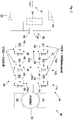
- FIG. 1 shows, in a schematic manner, an inverter circuit 10 according to an embodiment of the present disclosure.
- the inverter circuit 10 comprises a primary energy storage device 12, a plurality of switching stages 14, a drive control circuit 16 and an emergency control circuit 18.
- terminals of the energy storage device 12 and each of the switching stages 14 are connected by two different supply lines 20 and 22 for providing a direct current.
- Each of the switching stages 14 comprises a first semiconductor switch 24 connected to the positive supply line 20 and a second semiconductor switch 26 connected to the negative supply line 22.
- the drive control circuit 16 controls each one of the semiconductor switches 24 and 26 of each one of the switching stages 14 to generate a multi-phase AC signal for an external, electrical motor (not shown in Fig. 1 ), provided through a plurality of phase lines 28.
- an external, electrical motor not shown in Fig. 1
- phase lines 28 For example, in the case that a three-phase motor is to be controlled by the inverter circuit 10, three phase lines 28 connected to three corresponding switching stages 14 are used. Similarly, in the case of a six-phase electrical motor, six switching stages 14 and six corresponding phase lines 28 are used.
- the emergency control circuit 18 remains passive. That is to say, no control signals are provided by the emergency control circuit 18, and its output terminals remain in a high impedance state.
- the emergency control circuit 18 monitors the provision of control signals by the drive control circuit 16. In the case of a fault of the drive control circuit 16, the emergency control circuit 18 takes over control of the switching stages 14 of the inverter circuit 10. For example, if the control circuit 16 provides no or irregular output signals, the emergency control circuit 18 will provide control signals for the first semiconductor switches 24 and the second semiconductor switches 26 of all switching stages 14. To avoid any damage to the semiconductor switches 24 and 26, in this emergency operating mode, also referred to as active short circuit (ASC) mode, all phase lines 28 are shortened, either by the set of all first semiconductor switches 24 or all second semiconductor switches 26.
- ASC active short circuit
- FIG. 2 shows a circuit diagram of the electrical drive 30 comprising an inverter circuit 10 according to an embodiment of the present disclosure.
- the inverter circuit 10 of the electrical drive 30 comprises two energy storage devices, a battery 31, for example a rechargeable main battery of an electrical vehicle, and a direct current (DC) link capacitor 42 placed in electrical and physical proximity to the switching stages of the inverter circuit 10.
- the electrical drive 30 further comprises an alternating current (AC) motor 32 with permanent magnets such as an electrically commutated motor and/or a permanent field excitation motor.
- the AC motor 32 is an electric three-phase permanent-magnet synchronous motor (PMSM) connected to three switching stages 14a to 14c of the inverter circuit 10.
- PMSM permanent-magnet synchronous motor
- each of the switching stages 14a to 14c comprises two n-channel MOSFETs 34 and 36 respectively (as an alternative MISFETs may exemplarily be used).
- the first, in Figure 1 upper, n-channel MOSFET 34 of each of the stages 14a to 14c is connected in series with the second, in Figure 2 lower, n-channel MOSFET 36 of the same stage between a positive terminal 38 and a negative terminal 40 of a DC link capacitor 42.
- Each one of three phase lines 28a to 28c of the three-phase AC motor 32 is connected between the first MOSFET 34 and the second MOSFET 36 of one of the three switching stages 14a to 14c, respectively.
- the first n-channel MOSFETs 34 of the three switching stages 14a to 14c form a positive half-bridge 44 of the inverter circuit 10.
- the second n-channel MOSFETs 36 of the three switching stages 14a to 14c form a negative half-bridge 46 of the inverter circuit 10.
- switches S1 to S6 of the inverter circuit 10 provided by the MOSFETs 34 and 36, respectively are controlled by a drive control circuit (not shown in Figure 2 ) by selectively switching on individual switches as required to provide a desired torque of the AC motor 32.
- each one of the phase lines 28a to 28c can be selectively connected to the positive terminal 38 or the negative terminal 40 of the DC link capacitor 42 and/or another primary energy storage device, such as the battery 31.
- Suitable methods for the control of a three-phase AC motors 32 are known from the prior art and are therefore not described in detail here. In essence, a rotating electrical field is created within the electrical motor to control the speed and torque of its rotor as desired.
- a specific gate-source signal or voltage VGS in the following referred to as switch-on voltage VGSon, is provided to a terminal 48 of the respective switch.
- a second, typically lower gate-source signal VGS referred to as switch-off voltage VGSoff is provided to the respective gate terminal 48.
- the specific voltages may differ.
- VGSon corresponds to a voltage of +15 V
- VGSoff corresponds to a voltage of -4 V with respect to a reference potential such as electrical ground.
- other semiconductor switching elements may also be used.
- the switch-on voltage VGSon usually corresponds to +15 V and the switch-off voltage VGSoff corresponds to -15 V.
- such values are specified by the manufacturer of a given semiconductor switch.
- a fault occurs in the electrical drive 30, for example a fault in the drive control circuit 16 used to control the gate terminals 48 of the switches S1 to S6, the general control electronic of the electrical drive 30, or some other unexpected event, such as a lack of feedback within the control circuitry, the AC motor 32 will typically be free-spinning, and therefore act as a generator for the circuit shown in Figure 2 .
- a current generated by the free-spinning AC motor 32 can be used to recharge the DC link capacitor 42 or other primary energy storage devices to recuperate some of the kinetic energy of the system as electrical energy.
- controlled braking of the vehicle may be used to recharge a rechargeable main battery of the vehicle through controlled operation of the inverter circuit 10.
- the inverter circuit 10 by default will enter a state where all the MOSFETs 34 and 36 are turned off. In this case, the rotating energy of the motor will flow through the body diodes of the MOSFETs 34 and 36 or, in case IBGTs are used as switches S1 to S6, through their antiparallel diodes, and will start charging the DC link capacitor 42 and/or other primary energy storage device 10, such as the battery 31. This is a non-desired behavior because of a danger of overstressing the DC link capacitor 42 or charging the battery 31 with an overcurrent.
- an emergency control circuit (not shown in Figure 2 ) will take over control of the switches S1 to S6 to avoid an unacceptably high load current to the DC link capacitor 42 and/or battery 31.
- all first n-channel MOSFETs 34 are activated by providing a short-term control voltage VGSelevated to the gate terminals 48 of high-side switches S1, S3 and S5.
- VGSmax a maximum transient voltage allowed by the individual manufacturer of the MOSFETs 34. This has the advantage that it does not reduce the lifetime of the semiconductor switches. Using a significantly higher gate control voltage could result in overstressing the gates of the n-channel MOSFETs 34.
- a switch-off voltage VGSoff is provided to the gate terminals 48 of the second n-channel MOSFETs 36 corresponding to low-side switches S2, S4 and S6.
- the short-term control voltage VGSelevated provided to the gates 48 of the MOSFETs 34 during the relatively short ASC event is increased with respect to the normal switch-on voltage VGSon.
- a control voltage of 19 V is used, which is 4 V or around 25 % higher than the typical switch-on voltage of 15 V.
- the specific value of the short-term control voltage VGSelevated to be used in the ASC mode may differ depending on the type of semiconductor switch used. For example, for many commercially available semiconductor switches, a maximum allowable peak voltage or maximum transient voltage VGSmax for short-term provision to the gate terminal 48 may be specified by the respective manufacturer and used as the short-term control voltage VGSelevated.
- Figure 3 shows the output characteristic of a single semiconductor switch for two different gate control voltages, i.e. 15 V and 19 V.
- the voltage drop or bias voltage between the source and drain terminals of the respective switch is lower for the higher control gate supply.
- the channel resistance RDSon for a current of 180 A is reduced from 21.9 Q to 19.2 Q, an improvement by 14 %.
- This also gives a 14 % margin to the current part of the equation above, because the maximum energy is depending on the MOSFET chip geometry and therefore remains the same.
- a free-spinning AC motor with permanent magnets essentially acts as a current source.
- increasing a gate control voltage for a given speed of the AC motor 32 will result in a reduction of energy being dissipated in the channel region of the corresponding semiconductor switch.
- the amount of energy that can be safely dissipated by a semiconductor switch during a short-term event, such as an ASC event may also be specified by the manufacturer, allowing to safely dimension the components of the electrical drive 30.
- the emergency control circuit 18 quickly activates corresponding semiconductor switches 24 or 26 by the provision of a corresponding control voltage to the control gates 48 of high-side switches S1, S3 and S5, leading to a rapid increase of a current through these switches.
- the high-side switches S1, S3 and S5 are deactivated again, leading to a decrease of a current through these switches. Note that there is a time lag for both events, caused by the accumulation of charge carriers in a channel of the respective semiconductor switches.
- the energy E ASC being absorbed by the inverter circuit 10 is limited to a value determined by the maximum current and length of the ASC event. This energy level differs, depending on the provided gate voltage.
- the inverter circuit 10 absorbs an energy E ASC of 130 J during the ASC event. In case the gate terminals 48 of high-side switches S1, S3 and S5 are biased with 15 V, the inverter circuit 10 absorbs an energy E ASC of 160 J during the ASC event, i.e. 30 J or 23 % more energy.
- the electrical drive 30 may comprise further components to avoid any damage on the components of the inverter circuit 10 caused by a prolonged operation of the inverter circuit 10 in the ASC mode. While the ASC emergency mode is very fast to respond, as shown in Figure 4 , it does not provide a long-term solution for the control of the AC motor 32 in the case that the normal drive control circuit 16 cannot be reactivated quickly. Accordingly, the electrical drive 30 may comprise further components, such as a mechanical brake 50 which can be used to stop the electrical AC motor 32. Alternatively or in addition, one or several isolation relays 52 may be used to permanently disconnect the switching stages 14a to 14c from the battery 31 to avoid any damage to it, for example by overcharging.
- a braking chopper 54 may be used to shorten the positive terminal 38 and the negative terminal 40 of the DC link capacitor 42 using a shunt resistor.
- the isolation relays 52 are implemented as electromechanical relays and therefore have higher activation times than the semiconductor switches formed by the MOSFETs 34 or 36.
- the energy dissipated by the inverter circuit 10 can also be distributed over different switch groups as detailed below.
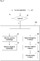
- FIG. 5 shows a flowchart of a method for operating the electrical drive 30.
- the electrical drive 30 is operated in a normal operation mode M1.
- the drive unit 30 switches to an ASC mode M2 of operation, wherein an emergency control circuit 18 takes over control of the inverter circuit 10.
- a step 62 all first semiconductor switches 24 of a positive half-bridge 44 are shortened to avoid a feedback of a high current to a primary energy storage device 12.
- the second semiconductor switches 26 of a negative half-bridge 46 are switched off to electrically separate the primary energy storage device 12 from the AC motor 32. This state is maintained for a predetermined amount of time, for example a few milliseconds, e.g. 2 to 5 ms.
- the second semiconductor switches 26 of the negative half-bridge 46 are shortened in a step 63 and the first semiconductor switches 24 of the positive half-bridge 44 are deactivated.
- one or more other emergency measures may be taken by the emergency control circuit 18.
- a mechanical brake 50 may be employed to slow down the AC motor 32.
- one or more isolation relays 52 may be controlled to physically disconnect a rechargeable battery 31 from the switching stages 14 of the inverter circuit 10.
- a braking chopper 54 may be used to electrically shorten terminals 38 and 40 of a DC link capacitor 42.
Abstract
Description
- The present disclosure relates to an inverter circuit for an electrical AC motor with permanent magnets, the circuit comprising a primary energy storage device, a plurality of switching stages, a drive control circuit and an emergency control circuit. The present disclosure further relates to an electrical drive comprising an inverter circuit and at least one AC motor with permanent magnets controlled by the inverter circuit. The present disclosure further relates to a method for controlling an electrical drive.
-
Document EP 0 742 637 A1 relates to a method and device for safe braking of an electrical drive. Using a clock control signal, the reaction speed and braking duration can be optimized. - Embodiments of the disclosure relate to improved circuits and methods for controlling an electrical drive, which are better suited to high power applications. For example, it is desirable to limit the thermal load on switching stages of an inverter circuit during abnormal operation states.
- According to a first aspect, an inverter circuit for an electrical AC motor with permanent magnets is provided. The inverter circuit comprises a primary energy storage device, a plurality of switching stages, a drive control circuit and an emergency control circuit. Each switching stage comprises a first semiconductor switch and a second semiconductor switch, the first semiconductor switches of the plurality of switching stages connected between a first terminal of the primary energy storage device and one of a plurality of phase lines of the electrical AC motor with permanent magnets, and the second semiconductor switches of the plurality of switching stages connected between a second terminal of the primary energy storage device and one of the plurality of phase lines. The drive control circuit is configured to selectively switch the first semiconductor switches and the second semiconductor switches to control a torque of the electrical motor during normal operation of the inverter circuit. The emergency control circuit is configured to switch on all of the first semiconductor switches or the second semiconductor switches by providing a short-term control voltage VGSelevated to control gates of the first semiconductor switches or the second semiconductor switches, respectively, to electrically connect the phase lines in case of an abnormal condition of the drive control circuit. The short-term control voltage VGSelevated exceeds a regular switch-on voltage VGSon provided to the control gates by the drive control circuit during normal operation of the inverter circuit.
- By providing a short-term control voltage VGSelevated that exceeds a regular switch-on voltage VGSon, the internal resistance of the semiconductor switches can be reduced, resulting in a reduced energy dissipation in the semiconductor switches of the switching stages. This in turn leads to a lower thermal load on the switching stages and helps to sustain a current generated by the electrical motor over a longer time period.
- According to at least one embodiment, a maximum transient voltage VGSmax specified for the first semiconductor switches or the second semiconductor switches may be used as the short-term control voltage VGSelevated. Use of the maximum transient voltage VGSmax, e.g. a maximum voltage specified by the semiconductor switch manufacturer, has the advantage that it does not lead to a significantly reduction of the lifetime of the semiconductor switches.
- According to at least one embodiment, the emergency control circuit is further configured to alternate between a first switching stage and a second switching stage. In the first switching stage, the short-term control voltage VGSelevated is provided to all of the first semiconductor switches, and in the second switching stage the short-term control voltage VGSelevated is provided to all of the second semiconductor switches. By alternating between activating the first and second semiconductor switches over time, the energy distribution can be spread over multiple semiconductor devices, thus further reducing the electrical and thermal load on individual switches.
- According to a second aspect of the disclosure, an electrical drive comprises an inverter circuit according to the first aspect and at least one AC motor with permanent magnets controlled by the inverter circuit. Such an electrical drive can survive an abnormal operation state for a longer time period without the need to provide a stronger inverter circuit for a given motor power or to provide a smaller motor for a given inverter strength.
- In at least one embodiment, the electrical drive further comprises an emergency response unit, configured to be activated in case of an abnormal condition of the drive control circuit, the emergency response unit having a predetermined activation time, wherein the emergency control circuit is configured to provide the short-term control voltage VGSelevated to control gates of the first semiconductor switches or the second semiconductor switches during the predetermined activation time. Provision of a relatively slow emergency response unit, such as a braking device, a brake chopper or an isolation relay, in addition to a faster acting emergency control circuit allows the primary energy storage to be protected rapidly during the onset of an abnormal operation condition. At the same time, the emergency response unit can take further actions to protect the inverter circuit itself from damage resulting from relatively high currents generated by the temporarily uncontrolled permanent field excitation motor.
- According to a third aspect, a method for controlling an electrical drive is provided. The method comprises:
- in a normal operating mode M1, selectively controlling at least one of first semiconductor switches and second semiconductor switches of a first half-bridge and a second half-bridge of an inverter circuit, respectively, to control an electrically AC motor with permanent magnets of the electrical drive; and
- in an active short circuit (ASC) mode M2, selectively switching on all of the first semiconductor switches or the second semiconductor switches to electrically shorten phase lines of the AC motor, wherein, in the ASC mode, a short-term control voltage VGSelevated is provided to control gates of the first semiconductor switches or the second semiconductor switches, wherein the short-term control voltage VGSelevated exceeds a regular switch-on voltage VGSon provided to the control gates during the normal operation mode M1.
- The devices and methods described above are suitable for high power applications, such as electrical drives of electrical vehicles or industrial equipment.
- As detailed above, the present disclosure comprises several aspects of an invention. Every feature described with respect to one of the aspects is also disclosed herein with respect to the other aspects, even if the respective feature is not explicitly mentioned in the context of the specific aspect.
- The accompanying figures are included to provide a further understanding. In the figures, elements of the same structure and/or functionality may be referenced by the same reference signs. It is to be understood that the embodiments shown in the figures are illustrative representations and are not necessarily drawn to scale.
-
Figure 1 shows, in a schematic manner, an inverter circuit according to an embodiment of the present disclosure. -
Figure 2 shows a circuit diagram of an electrical drive according to an embodiment of the present disclosure. -
Figure 3 shows an output characteristic of a single semiconductor switching element. -
Figure 4 shows an amount of energy dissipated over time by an inverter circuit. -
Figure 5 shows, in a schematic manner, a flowchart of a method for controlling an electrical drive. - While the invention is amenable to various modifications and alternative forms, specifics thereof have been shown by way of example in the figures and will be described in detail. It should be understood, however, that the intention is not to limit the invention to the exemplary embodiments described. On the contrary, the intention is to cover all modifications, equivalents, and alternatives falling within the scope of the invention defined by the appended claims.
-
Figure 1 shows, in a schematic manner, aninverter circuit 10 according to an embodiment of the present disclosure. Theinverter circuit 10 comprises a primaryenergy storage device 12, a plurality ofswitching stages 14, adrive control circuit 16 and anemergency control circuit 18. - As shown in
Figure 1 , terminals of theenergy storage device 12 and each of theswitching stages 14 are connected by twodifferent supply lines switching stages 14 comprises afirst semiconductor switch 24 connected to thepositive supply line 20 and asecond semiconductor switch 26 connected to thenegative supply line 22. - In a normal operation state, the
drive control circuit 16 controls each one of thesemiconductor switches switching stages 14 to generate a multi-phase AC signal for an external, electrical motor (not shown inFig. 1 ), provided through a plurality ofphase lines 28. For example, in the case that a three-phase motor is to be controlled by theinverter circuit 10, threephase lines 28 connected to threecorresponding switching stages 14 are used. Similarly, in the case of a six-phase electrical motor, sixswitching stages 14 and sixcorresponding phase lines 28 are used. During normal operation of theinverter circuit 10, theemergency control circuit 18 remains passive. That is to say, no control signals are provided by theemergency control circuit 18, and its output terminals remain in a high impedance state. - While the
inverter circuit 10 is operating, theemergency control circuit 18 monitors the provision of control signals by thedrive control circuit 16. In the case of a fault of thedrive control circuit 16, theemergency control circuit 18 takes over control of theswitching stages 14 of theinverter circuit 10. For example, if thecontrol circuit 16 provides no or irregular output signals, theemergency control circuit 18 will provide control signals for thefirst semiconductor switches 24 and thesecond semiconductor switches 26 of allswitching stages 14. To avoid any damage to thesemiconductor switches phase lines 28 are shortened, either by the set of allfirst semiconductor switches 24 or allsecond semiconductor switches 26. This is achieved by providing a short-term control voltage VGSelevated to control gates of the first orsecond semiconductor switches second semiconductor switches drive control circuit 16 during normal operation of theinverter circuit 10. - Details of the
inverter circuit 10 and its operation are explained below with regard to anelectrical drive 30.Figure 2 shows a circuit diagram of theelectrical drive 30 comprising aninverter circuit 10 according to an embodiment of the present disclosure. In the described embodiment, theinverter circuit 10 of theelectrical drive 30 comprises two energy storage devices, abattery 31, for example a rechargeable main battery of an electrical vehicle, and a direct current (DC)link capacitor 42 placed in electrical and physical proximity to the switching stages of theinverter circuit 10. Theelectrical drive 30 further comprises an alternating current (AC)motor 32 with permanent magnets such as an electrically commutated motor and/or a permanent field excitation motor. In the described embodiment, theAC motor 32 is an electric three-phase permanent-magnet synchronous motor (PMSM) connected to threeswitching stages 14a to 14c of theinverter circuit 10. - In the embodiment shown in
Figure 2 , each of theswitching stages 14a to 14c comprises two n-channel MOSFETs Figure 1 upper, n-channel MOSFET 34 of each of thestages 14a to 14c is connected in series with the second, inFigure 2 lower, n-channel MOSFET 36 of the same stage between apositive terminal 38 and anegative terminal 40 of aDC link capacitor 42. Each one of threephase lines 28a to 28c of the three-phase AC motor 32 is connected between thefirst MOSFET 34 and thesecond MOSFET 36 of one of the threeswitching stages 14a to 14c, respectively. Together, the first n-channel MOSFETs 34 of the three switchingstages 14a to 14c form a positive half-bridge 44 of theinverter circuit 10. Correspondingly, the second n-channel MOSFETs 36 of the three switchingstages 14a to 14c form a negative half-bridge 46 of theinverter circuit 10. During normal operation of theelectrical drive 30, switches S1 to S6 of theinverter circuit 10 provided by theMOSFETs Figure 2 ) by selectively switching on individual switches as required to provide a desired torque of theAC motor 32. For this purpose, each one of thephase lines 28a to 28c can be selectively connected to thepositive terminal 38 or thenegative terminal 40 of theDC link capacitor 42 and/or another primary energy storage device, such as thebattery 31. Suitable methods for the control of a three-phase AC motors 32 are known from the prior art and are therefore not described in detail here. In essence, a rotating electrical field is created within the electrical motor to control the speed and torque of its rotor as desired. - To switch on one of the switches S1 to S6, a specific gate-source signal or voltage VGS, in the following referred to as switch-on voltage VGSon, is provided to a
terminal 48 of the respective switch. Inversely, to deactivate one of the switches, a second, typically lower gate-source signal VGS, referred to as switch-off voltage VGSoff is provided to therespective gate terminal 48. Depending on the type of the semiconductor switch used, the specific voltages may differ. For example, for the n-channel MOSFETs Figure 2 , VGSon corresponds to a voltage of +15 V, and VGSoff corresponds to a voltage of -4 V with respect to a reference potential such as electrical ground. However, other semiconductor switching elements may also be used. For example, in the case that IGBTs are used as switching elements, the switch-on voltage VGSon usually corresponds to +15 V and the switch-off voltage VGSoff corresponds to -15 V. Typically, such values are specified by the manufacturer of a given semiconductor switch. - If a fault occurs in the
electrical drive 30, for example a fault in thedrive control circuit 16 used to control thegate terminals 48 of the switches S1 to S6, the general control electronic of theelectrical drive 30, or some other unexpected event, such as a lack of feedback within the control circuitry, theAC motor 32 will typically be free-spinning, and therefore act as a generator for the circuit shown inFigure 2 . In a controlled mode of operation, a current generated by the free-spinningAC motor 32 can be used to recharge theDC link capacitor 42 or other primary energy storage devices to recuperate some of the kinetic energy of the system as electrical energy. For example, for an electrical vehicle, controlled braking of the vehicle may be used to recharge a rechargeable main battery of the vehicle through controlled operation of theinverter circuit 10. - However, if no gate-source voltage VGS is provided to the switches S1 to S6, the
inverter circuit 10 by default will enter a state where all the MOSFETs 34 and 36 are turned off. In this case, the rotating energy of the motor will flow through the body diodes of theMOSFETs DC link capacitor 42 and/or other primaryenergy storage device 10, such as thebattery 31. This is a non-desired behavior because of a danger of overstressing theDC link capacitor 42 or charging thebattery 31 with an overcurrent. Thus, in the case that theinverter circuit 10 cannot be controlled in a suitable manner, an emergency control circuit (not shown inFigure 2 ) will take over control of the switches S1 to S6 to avoid an unacceptably high load current to theDC link capacitor 42 and/orbattery 31. - For this purpose, all semiconductor switches of one of the positive or negative half-
bridges phase lines 28a to 28c of theAC motor 32. In this way, the rotating energy of theAC motor 32 at the time of the fault is transformed into heat on the switches S1 to S6 and dissipated at a cooling system of theinverter circuit 10. - In the example shown in
Figure 2 , all first n-channel MOSFETs 34 are activated by providing a short-term control voltage VGSelevated to thegate terminals 48 of high-side switches S1, S3 and S5. In the described example, a maximum transient voltage allowed by the individual manufacturer of theMOSFETs 34, referred to as VGSmax, is used. This has the advantage that it does not reduce the lifetime of the semiconductor switches. Using a significantly higher gate control voltage could result in overstressing the gates of the n-channel MOSFETs 34. At the same time, a switch-off voltage VGSoff is provided to thegate terminals 48 of the second n-channel MOSFETs 36 corresponding to low-side switches S2, S4 and S6. However, as detailed later, it is also possible to activate the switches of the negative half-bridge 46 and open the switches of the positive half-bridge 44. - In this ASC mode of operation, a relatively high current flows from the
respective phase lines 28 of theAC motor 32 through theMOSFETs 34 in a short-circuit, resulting in a high energy dissipation and thus heating of the semiconductor body of each one of theMOSFETs 34. If theMOSFETs 34 temperature rises above a certain level, destruction of the semiconductor chip will occur due to the elevated temperature. The capability of theMOSFETs 34 and by extension, theinverter circuit 10, to survive such an ASC event is given by the maximum energy which theMOSFETs 34 can sustain. The energy dissipated by theMOSFETs 34 during the ASC event of time duration t1 is given by
drive 30 by other means as detailed below. - To reduce the internal channel resistance RDSon of the
MOSFETs 34, the short-term control voltage VGSelevated provided to thegates 48 of theMOSFETs 34 during the relatively short ASC event is increased with respect to the normal switch-on voltage VGSon. For example, in the described embodiment, a control voltage of 19 V is used, which is 4 V or around 25 % higher than the typical switch-on voltage of 15 V. - It is noted that the specific value of the short-term control voltage VGSelevated to be used in the ASC mode may differ depending on the type of semiconductor switch used. For example, for many commercially available semiconductor switches, a maximum allowable peak voltage or maximum transient voltage VGSmax for short-term provision to the
gate terminal 48 may be specified by the respective manufacturer and used as the short-term control voltage VGSelevated. - The effects of such a control method is shown in
Figures 3 and 4. Figure 3 shows the output characteristic of a single semiconductor switch for two different gate control voltages, i.e. 15 V and 19 V. Taking a 750 V SiC MOSFET as an example, it can be seen that, for the same current flowing through the semiconductor switch, the voltage drop or bias voltage between the source and drain terminals of the respective switch is lower for the higher control gate supply. For example, the channel resistance RDSon for a current of 180 A is reduced from 21.9 Q to 19.2 Q, an improvement by 14 %. This also gives a 14 % margin to the current part of the equation above, because the maximum energy is depending on the MOSFET chip geometry and therefore remains the same. Decreasing the channel resistance RDSon by 14 % allows the ASC event current to increase to
AC motor 32 will result in a reduction of energy being dissipated in the channel region of the corresponding semiconductor switch. The amount of energy that can be safely dissipated by a semiconductor switch during a short-term event, such as an ASC event, may also be specified by the manufacturer, allowing to safely dimension the components of theelectrical drive 30. - This is shown in more detail in
Figure 4 , showing the total amount of energy being dissipated in theinverter circuit 10 during an ASC event. In the example, the ASC event results in a current of 1800 A and last for 10 ms. After this time, other means of control take over as described in further detail below. - After detection of the loss of control at t=0 ms, the
emergency control circuit 18 quickly activates corresponding semiconductor switches 24 or 26 by the provision of a corresponding control voltage to thecontrol gates 48 of high-side switches S1, S3 and S5, leading to a rapid increase of a current through these switches. At t=10 ms, the high-side switches S1, S3 and S5 are deactivated again, leading to a decrease of a current through these switches. Note that there is a time lag for both events, caused by the accumulation of charge carriers in a channel of the respective semiconductor switches. The energy EASC being absorbed by theinverter circuit 10 is limited to a value determined by the maximum current and length of the ASC event. This energy level differs, depending on the provided gate voltage. In the described example, in case thegate terminals 48 of high-side switches S1, S3 and S5 are biased with 19 V, theinverter circuit 10 absorbs an energy EASC of 130 J during the ASC event. In case thegate terminals 48 of high-side switches S1, S3 and S5 are biased with 15 V, theinverter circuit 10 absorbs an energy EASC of 160 J during the ASC event, i.e. 30 J or 23 % more energy. - Coming back to the circuit diagram of
Figure 2 , theelectrical drive 30 may comprise further components to avoid any damage on the components of theinverter circuit 10 caused by a prolonged operation of theinverter circuit 10 in the ASC mode. While the ASC emergency mode is very fast to respond, as shown inFigure 4 , it does not provide a long-term solution for the control of theAC motor 32 in the case that the normaldrive control circuit 16 cannot be reactivated quickly. Accordingly, theelectrical drive 30 may comprise further components, such as amechanical brake 50 which can be used to stop theelectrical AC motor 32. Alternatively or in addition, one or several isolation relays 52 may be used to permanently disconnect the switching stages 14a to 14c from thebattery 31 to avoid any damage to it, for example by overcharging. Moreover, abraking chopper 54 may be used to shorten thepositive terminal 38 and thenegative terminal 40 of theDC link capacitor 42 using a shunt resistor. Typically, the isolation relays 52 are implemented as electromechanical relays and therefore have higher activation times than the semiconductor switches formed by theMOSFETs inverter circuit 10 can also be distributed over different switch groups as detailed below. -
Figure 5 shows a flowchart of a method for operating theelectrical drive 30. Initially, theelectrical drive 30 is operated in a normal operation mode M1. In case a failure during normal operation is detected instep 61, thedrive unit 30 switches to an ASC mode M2 of operation, wherein anemergency control circuit 18 takes over control of theinverter circuit 10. - In the example shown in
Figure 4 , in astep 62, all first semiconductor switches 24 of a positive half-bridge 44 are shortened to avoid a feedback of a high current to a primaryenergy storage device 12. At the same time, the second semiconductor switches 26 of a negative half-bridge 46 are switched off to electrically separate the primaryenergy storage device 12 from theAC motor 32. This state is maintained for a predetermined amount of time, for example a few milliseconds, e.g. 2 to 5 ms. Thereafter, to avoid overheating of the first semiconductor switches 24, the second semiconductor switches 26 of the negative half-bridge 46 are shortened in astep 63 and the first semiconductor switches 24 of the positive half-bridge 44 are deactivated. - In
optional steps emergency control circuit 18. For example, instep 64, amechanical brake 50 may be employed to slow down theAC motor 32. Moreover, in astep 65, one or more isolation relays 52 may be controlled to physically disconnect arechargeable battery 31 from the switching stages 14 of theinverter circuit 10. In astep 66, abraking chopper 54 may be used to electrically shortenterminals DC link capacitor 42. - The embodiments shown in the
Figures 1 to 5 as stated represent exemplary embodiments of the improved devices and methods for their operation. Therefore, they do not constitute a complete list of all embodiments according to the improved devices and methods. Actual devices and methods may vary from the embodiments shown in terms of their specific components, configurations, signals and processing steps, for example. -
- 10
- inverter
- 12
- primary energy storage device
- 14
- switching stage
- 16
- drive control circuit
- 18
- emergency control circuit
- 20
- positive supply line
- 22
- negative supply line
- 24
- first semiconductor switch
- 26
- second semiconductor switch
- 28
- phase line
- 30
- electrical drive
- 31
- battery
- 32
- AC motor
- 34
- first (n-channel) MOSFET
- 36
- second (n-channel) MOSFET
- 38
- positive terminal
- 40
- negative terminal
- 42
- DC link capacitor
- 44
- positive half-bridge
- 46
- negative half-bridge
- 48
- gate terminal
- 50
- mechanical brake
- 52
- isolation relay
- 54
- braking chopper
- 61-66
- method steps
- M1
- normal operation mode
- M2
- ASC mode
- VGS
- gate-source voltage
- VGSon
- switch-on voltage
- VGSoff
- switch-off voltage
- VGSmax
- maximum transient voltage
- VGSelevated
- short-term control voltage
Claims (15)
- An inverter circuit (10) for an electrical AC motor (32) with permanent magnets, comprising- a primary energy storage device (12);- a plurality of switching stages (14), each switching stage (14) comprising a first semiconductor switch (24) and a second semiconductor switch (26), the first semiconductor switches (24) connected between a first terminal of the primary energy storage device (12) and one of a plurality of phase lines (28) of the electrical AC motor (32) with permanent magnets, and the second semiconductor switches (26) connected between a second terminal of the primary energy storage device (12) and one of the plurality of phase lines (28;- a drive control circuit (16), configured to selectively switch the first semiconductor switches (24) and the second semiconductor switches (26) to control a torque of the electrical AC motor (32) during normal operation of the inverter circuit (10); and- an emergency control circuit (18), configured to switch on all of the first semiconductor switches (24) or the second semiconductor switches (26) by providing a short-term control voltage VGSelevated to control gates (48) of the first semiconductor switches (24) or the second semiconductor switches (26), respectively, to electrically connect the phase lines (28) in case of an abnormal condition of the drive control circuit (16), wherein the short-term control voltage VGSelevated exceeds a regular switch-on voltage VGSon provided to the control gates (48) by the drive control circuit (16) during normal operation of the inverter circuit (10).
- The inverter circuit (10) of claim 1, wherein the short-term control voltage VGSelevated corresponds to a maximum transient voltage VGSmax specified for the first semiconductor switches (24) or the second semiconductor switches (26).
- The inverter circuit (10) of claim 1 or 2, wherein the short-term control voltage VGSelevated exceeds the regular switch-on voltage VGSon by at least one of 15 % or 4 V.
- The inverter circuit (10) of any one of claims 1 to 3, wherein the emergency control circuit (18) is configured, in a first switching state during a first time period, to provide the short-term control voltage VGSelevated to the control gates (48) of all first semiconductor switches (24), and to provide a switch-off voltage VGSoff to the control gates (48) of all second semiconductor switches (26).
- The inverter circuit (10) of claim 4, wherein the emergency control circuit (18) is further configured, in a second switching state during a second time period, to provide the short-term control voltage VGSelevated to the control gates (48) of all second semiconductor switches (26) and to provide the switch-off voltage VGSoff to the control gates (48) of all first semiconductor switches (24), the second time period following the first time period.
- The inverter circuit (10) of claim 5, wherein the emergency control circuit (18) is further configured to alternate between the first switching state and the second switching state.
- The inverter of any one of claims 1 to 6, wherein the primary energy storage device (10) comprises at least one of a DC link capacitor (42) or a rechargeable battery (31) configured for storing electrical energy recuperated during deceleration of the electrical AC motor (32) during normal operation of the inverter circuit (10).
- The inverter circuit (10) of any one of claims 1 to 7, wherein the first semiconductor switches (24) and the second semiconductor switches (26) comprise at least one of MISFETs, MOSFETs or IGBTs (36, 34) having a maximum allowed gate voltage exceeding the switch-on voltage VGSon.
- An electrical drive (30), comprising:- an inverter circuit (10) according to one of claims 1 to 8; and- at least one AC motor (32) with permanent magnets controlled by the inverter circuit (10).
- The electrical drive (30) of claim 9, further comprising an emergency response unit, configured to be activated in case of an abnormal condition of the drive control circuit (16), the emergency response unit having a predetermined activation time, wherein the emergency control circuit (18) is configured to provide the short-term control voltage VGSelevated to the control gates (48) of the first semiconductor switches (24) or the second semiconductor switches (26) during the predetermined activation time.
- The electrical drive (30) of claim 10, wherein the emergency response unit comprises at least one of the following:- a braking device for the AC motor (32);- at least one electrical isolation switch for electrically isolating at least parts of the primary energy storage device (12) from the plurality of switching stages (14); and- a braking chopper (54) for electrically bypassing at least parts of the primary energy storage device (12).
- The electrical drive (30) of any one of claims 9 to 11, wherein the AC motor (32) comprises at least one of an electrically commutated motor, a permanent field excitation motor, and a permanent-magnet synchronous motor (PMSM).
- A method for controlling an electrical drive (30), comprising:- in a normal operating mode M1, selectively controlling at least one of first semiconductor switches (24) and second semiconductor switches (26) of a first half-bridge (44) and a second half-bridge (46) of an inverter circuit (10), respectively, to control an AC motor (32) with permanent magnets of the electrical drive (30); and- in an active short circuit, ASC, mode M2, selectively switching on all of the first second semiconductor switches (24) or the second semiconductor switches (26) to electrically shorten phase lines (28) of the AC motor (32), wherein, in the ASC mode M2, a short-term control voltage VGSelevated is provided to control gates (48) of the first semiconductor switches (24) or the second semiconductor switches (26), wherein the short-term control voltage VGSelevated exceeds a regular switch-on voltage VGSon provided to the control gates (48) during the normal operation mode M1.
- The method of claim 13, further comprising:- electrically isolating or shortening a primary energy storage device (12) connected to a primary side of the inverter circuit (10) during the ASC mode M2.
- The method of claim 13 or 14, wherein the short-term control voltage VGSelevated corresponds to a maximum transient voltage VGSmax specified for the first semiconductor switches (24) or the second semiconductor switches (26).
Priority Applications (3)
| Application Number | Priority Date | Filing Date | Title |
|---|---|---|---|
| EP21168334.7A EP4075652A1 (en) | 2021-04-14 | 2021-04-14 | Inverter circuit for an electrical ac motor, electrical drive and method for controlling an electrical drive |
| PCT/EP2022/056477 WO2022218627A1 (en) | 2021-04-14 | 2022-03-14 | Inverter circuit for an electrical ac motor, electrical drive and method for controlling an electrical drive |
| JP2023600138U JP3246096U (en) | 2021-04-14 | 2022-03-14 | Inverter circuit for electric AC motor, electric drive and method for controlling electric drive |
Applications Claiming Priority (1)
| Application Number | Priority Date | Filing Date | Title |
|---|---|---|---|
| EP21168334.7A EP4075652A1 (en) | 2021-04-14 | 2021-04-14 | Inverter circuit for an electrical ac motor, electrical drive and method for controlling an electrical drive |
Publications (1)
| Publication Number | Publication Date |
|---|---|
| EP4075652A1 true EP4075652A1 (en) | 2022-10-19 |
Family
ID=75529855
Family Applications (1)
| Application Number | Title | Priority Date | Filing Date |
|---|---|---|---|
| EP21168334.7A Pending EP4075652A1 (en) | 2021-04-14 | 2021-04-14 | Inverter circuit for an electrical ac motor, electrical drive and method for controlling an electrical drive |
Country Status (3)
| Country | Link |
|---|---|
| EP (1) | EP4075652A1 (en) |
| JP (1) | JP3246096U (en) |
| WO (1) | WO2022218627A1 (en) |
Citations (6)
| Publication number | Priority date | Publication date | Assignee | Title |
|---|---|---|---|---|
| EP0742637A1 (en) | 1995-05-11 | 1996-11-13 | Siemens Aktiengesellschaft | Method and device for safely braking of an electric drive |
| WO2011139269A1 (en) * | 2010-05-04 | 2011-11-10 | Johnson Controls Technology Company | Variable speed drive |
| US20130181731A1 (en) * | 2012-01-13 | 2013-07-18 | Takao Kanzaki | Inverter |
| US20170093323A1 (en) * | 2014-03-31 | 2017-03-30 | Aisin Aw Co., Ltd. | Inverter control device |
| CN109130864A (en) * | 2018-07-25 | 2019-01-04 | 江苏力信电气技术有限公司 | Electric car low pressure power-down protection circuit |
| US20190137347A1 (en) * | 2016-04-29 | 2019-05-09 | Robert Bosch Gmbh | Switching element having temperature monitoring and method for temperature monitoring |
Family Cites Families (1)
| Publication number | Priority date | Publication date | Assignee | Title |
|---|---|---|---|---|
| DE102012224336A1 (en) * | 2012-12-21 | 2014-06-26 | Ge Energy Power Conversion Gmbh | Method for operating an electric power converter and electric power converters |
-
2021
- 2021-04-14 EP EP21168334.7A patent/EP4075652A1/en active Pending
-
2022
- 2022-03-14 WO PCT/EP2022/056477 patent/WO2022218627A1/en active Application Filing
- 2022-03-14 JP JP2023600138U patent/JP3246096U/en active Active
Patent Citations (6)
| Publication number | Priority date | Publication date | Assignee | Title |
|---|---|---|---|---|
| EP0742637A1 (en) | 1995-05-11 | 1996-11-13 | Siemens Aktiengesellschaft | Method and device for safely braking of an electric drive |
| WO2011139269A1 (en) * | 2010-05-04 | 2011-11-10 | Johnson Controls Technology Company | Variable speed drive |
| US20130181731A1 (en) * | 2012-01-13 | 2013-07-18 | Takao Kanzaki | Inverter |
| US20170093323A1 (en) * | 2014-03-31 | 2017-03-30 | Aisin Aw Co., Ltd. | Inverter control device |
| US20190137347A1 (en) * | 2016-04-29 | 2019-05-09 | Robert Bosch Gmbh | Switching element having temperature monitoring and method for temperature monitoring |
| CN109130864A (en) * | 2018-07-25 | 2019-01-04 | 江苏力信电气技术有限公司 | Electric car low pressure power-down protection circuit |
Also Published As
| Publication number | Publication date |
|---|---|
| JP3246096U (en) | 2024-03-21 |
| WO2022218627A1 (en) | 2022-10-20 |
Similar Documents
| Publication | Publication Date | Title |
|---|---|---|
| US9154051B2 (en) | Operating state circuit for an inverter and method for setting operating states of an inverter | |
| CN107508528B (en) | Self-limiting active discharge circuit of electric vehicle inverter | |
| JP6761014B2 (en) | Inverter for electric vehicles | |
| US9640972B2 (en) | Controlled switch-off of a power switch | |
| US9548675B2 (en) | Method and device for discharging an inverter capacitor | |
| US20170302189A1 (en) | Device for temporarily taking over electrical current from an energy transfer or distribution device, when needed | |
| US20110260534A1 (en) | SSPC for AC Power Distribution | |
| US20220348084A1 (en) | Discharge apparatus for an electrical drive arrangement of a vehicle and electrical drive arrangement comprising the discharge apparatus | |
| JP2007533284A (en) | Inverter / bridge short-circuit protection scheme | |
| CN109075581B (en) | Battery disconnection circuit and method for controlling battery disconnection circuit | |
| US11368083B2 (en) | Method and device for discharging a DC-link capacitor | |
| EP2149988B1 (en) | Switching device, high power supply system and methods for switching high power | |
| CN111591140A (en) | Battery management system and vehicle | |
| JP2013198256A (en) | Electric vehicle | |
| CN110073592B (en) | Protection device for an electric drive system, electric drive system and method for operating an electric drive system | |
| US20120229068A1 (en) | Inverter | |
| KR20180128155A (en) | Power converting apparatus | |
| EP4075652A1 (en) | Inverter circuit for an electrical ac motor, electrical drive and method for controlling an electrical drive | |
| US20120217918A1 (en) | Inverter | |
| CN112534720A (en) | Driving circuit | |
| US11271495B2 (en) | Intermediate circuit coupling in drive assemblies | |
| WO2019145044A1 (en) | Protection of switching cells for a voltage source converter | |
| US8598835B2 (en) | Protection circuit for a drive circuit of a permanent magnet motor and corresponding system | |
| US20240088812A1 (en) | Active Discharge of the DC Link Capacitor of a Three-Phase Inverter by Way of Rotating Half-Bridge Short-Circuits | |
| CN113852047A (en) | Inverter for an electric machine, electric machine having such an inverter, and steering system having such an electric machine |
Legal Events
| Date | Code | Title | Description |
|---|---|---|---|
| PUAI | Public reference made under article 153(3) epc to a published international application that has entered the european phase |
Free format text: ORIGINAL CODE: 0009012 |
|
| STAA | Information on the status of an ep patent application or granted ep patent |
Free format text: STATUS: THE APPLICATION HAS BEEN PUBLISHED |
|
| AK | Designated contracting states |
Kind code of ref document: A1 Designated state(s): AL AT BE BG CH CY CZ DE DK EE ES FI FR GB GR HR HU IE IS IT LI LT LU LV MC MK MT NL NO PL PT RO RS SE SI SK SM TR |
|
| STAA | Information on the status of an ep patent application or granted ep patent |
Free format text: STATUS: REQUEST FOR EXAMINATION WAS MADE |
|
| 17P | Request for examination filed |
Effective date: 20221017 |
|
| RBV | Designated contracting states (corrected) |
Designated state(s): AL AT BE BG CH CY CZ DE DK EE ES FI FR GB GR HR HU IE IS IT LI LT LU LV MC MK MT NL NO PL PT RO RS SE SI SK SM TR |
|
| STAA | Information on the status of an ep patent application or granted ep patent |
Free format text: STATUS: EXAMINATION IS IN PROGRESS |
|
| 17Q | First examination report despatched |
Effective date: 20230118 |
|
| P01 | Opt-out of the competence of the unified patent court (upc) registered |
Effective date: 20230527 |
|
| RAP1 | Party data changed (applicant data changed or rights of an application transferred) |
Owner name: HITACHI ENERGY LTD |
|
| GRAP | Despatch of communication of intention to grant a patent |
Free format text: ORIGINAL CODE: EPIDOSNIGR1 |
|
| STAA | Information on the status of an ep patent application or granted ep patent |
Free format text: STATUS: GRANT OF PATENT IS INTENDED |
|
| RIC1 | Information provided on ipc code assigned before grant |
Ipc: H02P 27/06 20060101ALI20240112BHEP Ipc: H02M 1/08 20060101ALI20240112BHEP Ipc: B60L 3/00 20190101ALI20240112BHEP Ipc: H02M 7/5387 20070101ALI20240112BHEP Ipc: H02M 1/32 20070101AFI20240112BHEP |
|
| INTG | Intention to grant announced |
Effective date: 20240129 |