EP4075475A1 - Spherical aberration adjustment cathode lens, spherical aberration correction electrostatic lens, electron spectroscope, and photoemission electron microscope - Google Patents
Spherical aberration adjustment cathode lens, spherical aberration correction electrostatic lens, electron spectroscope, and photoemission electron microscope Download PDFInfo
- Publication number
- EP4075475A1 EP4075475A1 EP20903239.0A EP20903239A EP4075475A1 EP 4075475 A1 EP4075475 A1 EP 4075475A1 EP 20903239 A EP20903239 A EP 20903239A EP 4075475 A1 EP4075475 A1 EP 4075475A1
- Authority
- EP
- European Patent Office
- Prior art keywords
- lens
- spherical aberration
- electrode
- point source
- electrostatic lens
- Prior art date
- Legal status (The legal status is an assumption and is not a legal conclusion. Google has not performed a legal analysis and makes no representation as to the accuracy of the status listed.)
- Pending
Links
- 230000004075 alteration Effects 0.000 title claims description 182
- 238000012937 correction Methods 0.000 title claims description 109
- 238000000605 extraction Methods 0.000 claims abstract description 94
- 239000002245 particle Substances 0.000 claims abstract description 40
- 230000005684 electric field Effects 0.000 claims description 23
- 230000001133 acceleration Effects 0.000 claims description 17
- 239000000284 extract Substances 0.000 claims description 3
- 238000009826 distribution Methods 0.000 description 55
- 238000010586 diagram Methods 0.000 description 27
- 238000005259 measurement Methods 0.000 description 22
- 241001232464 Delma Species 0.000 description 13
- 238000000034 method Methods 0.000 description 13
- 230000035945 sensitivity Effects 0.000 description 12
- 239000007787 solid Substances 0.000 description 11
- 238000001228 spectrum Methods 0.000 description 11
- 238000004458 analytical method Methods 0.000 description 10
- 230000000694 effects Effects 0.000 description 7
- 238000003384 imaging method Methods 0.000 description 7
- 239000000463 material Substances 0.000 description 7
- 230000008859 change Effects 0.000 description 6
- 239000006185 dispersion Substances 0.000 description 6
- 238000010894 electron beam technology Methods 0.000 description 6
- 238000002834 transmittance Methods 0.000 description 6
- 238000013459 approach Methods 0.000 description 5
- 230000007423 decrease Effects 0.000 description 5
- 238000013461 design Methods 0.000 description 5
- 238000011161 development Methods 0.000 description 5
- 239000010409 thin film Substances 0.000 description 5
- 238000004002 angle-resolved photoelectron spectroscopy Methods 0.000 description 4
- 238000001093 holography Methods 0.000 description 4
- 238000001420 photoelectron spectroscopy Methods 0.000 description 4
- 239000000126 substance Substances 0.000 description 4
- OKTJSMMVPCPJKN-UHFFFAOYSA-N Carbon Chemical compound [C] OKTJSMMVPCPJKN-UHFFFAOYSA-N 0.000 description 3
- 239000006096 absorbing agent Substances 0.000 description 3
- 238000004364 calculation method Methods 0.000 description 3
- 238000001514 detection method Methods 0.000 description 3
- 230000001678 irradiating effect Effects 0.000 description 3
- 238000013507 mapping Methods 0.000 description 3
- 230000003287 optical effect Effects 0.000 description 3
- 238000001478 photoelectron diffraction Methods 0.000 description 3
- 238000012545 processing Methods 0.000 description 3
- 238000004611 spectroscopical analysis Methods 0.000 description 3
- 230000005469 synchrotron radiation Effects 0.000 description 3
- 238000004833 X-ray photoelectron spectroscopy Methods 0.000 description 2
- 239000011358 absorbing material Substances 0.000 description 2
- 230000000903 blocking effect Effects 0.000 description 2
- 239000002019 doping agent Substances 0.000 description 2
- 238000001941 electron spectroscopy Methods 0.000 description 2
- 238000005516 engineering process Methods 0.000 description 2
- 229910002804 graphite Inorganic materials 0.000 description 2
- 239000010439 graphite Substances 0.000 description 2
- 150000002500 ions Chemical class 0.000 description 2
- 238000004519 manufacturing process Methods 0.000 description 2
- 239000000203 mixture Substances 0.000 description 2
- 238000011160 research Methods 0.000 description 2
- 238000004402 ultra-violet photoelectron spectroscopy Methods 0.000 description 2
- 238000009825 accumulation Methods 0.000 description 1
- 230000009471 action Effects 0.000 description 1
- 238000004774 atomic orbital Methods 0.000 description 1
- 230000008901 benefit Effects 0.000 description 1
- 230000005540 biological transmission Effects 0.000 description 1
- 230000015572 biosynthetic process Effects 0.000 description 1
- 230000003247 decreasing effect Effects 0.000 description 1
- 238000011156 evaluation Methods 0.000 description 1
- 230000005284 excitation Effects 0.000 description 1
- 229910021389 graphene Inorganic materials 0.000 description 1
- 239000012212 insulator Substances 0.000 description 1
- 238000005457 optimization Methods 0.000 description 1
- 239000011368 organic material Substances 0.000 description 1
- 239000011148 porous material Substances 0.000 description 1
- 230000008569 process Effects 0.000 description 1
- 230000005855 radiation Effects 0.000 description 1
- 238000000682 scanning probe acoustic microscopy Methods 0.000 description 1
- 239000004065 semiconductor Substances 0.000 description 1
- 238000010200 validation analysis Methods 0.000 description 1
Images


Classifications
-
- H—ELECTRICITY
- H01—ELECTRIC ELEMENTS
- H01J—ELECTRIC DISCHARGE TUBES OR DISCHARGE LAMPS
- H01J37/00—Discharge tubes with provision for introducing objects or material to be exposed to the discharge, e.g. for the purpose of examination or processing thereof
- H01J37/02—Details
- H01J37/04—Arrangements of electrodes and associated parts for generating or controlling the discharge, e.g. electron-optical arrangement or ion-optical arrangement
- H01J37/10—Lenses
- H01J37/12—Lenses electrostatic
-
- H—ELECTRICITY
- H01—ELECTRIC ELEMENTS
- H01J—ELECTRIC DISCHARGE TUBES OR DISCHARGE LAMPS
- H01J37/00—Discharge tubes with provision for introducing objects or material to be exposed to the discharge, e.g. for the purpose of examination or processing thereof
- H01J37/02—Details
- H01J37/04—Arrangements of electrodes and associated parts for generating or controlling the discharge, e.g. electron-optical arrangement or ion-optical arrangement
- H01J37/05—Electron or ion-optical arrangements for separating electrons or ions according to their energy or mass
-
- H—ELECTRICITY
- H01—ELECTRIC ELEMENTS
- H01J—ELECTRIC DISCHARGE TUBES OR DISCHARGE LAMPS
- H01J37/00—Discharge tubes with provision for introducing objects or material to be exposed to the discharge, e.g. for the purpose of examination or processing thereof
- H01J37/02—Details
- H01J37/04—Arrangements of electrodes and associated parts for generating or controlling the discharge, e.g. electron-optical arrangement or ion-optical arrangement
- H01J37/153—Electron-optical or ion-optical arrangements for the correction of image defects, e.g. stigmators
-
- H—ELECTRICITY
- H01—ELECTRIC ELEMENTS
- H01J—ELECTRIC DISCHARGE TUBES OR DISCHARGE LAMPS
- H01J37/00—Discharge tubes with provision for introducing objects or material to be exposed to the discharge, e.g. for the purpose of examination or processing thereof
- H01J37/26—Electron or ion microscopes; Electron or ion diffraction tubes
- H01J37/285—Emission microscopes, e.g. field-emission microscopes
-
- H—ELECTRICITY
- H01—ELECTRIC ELEMENTS
- H01J—ELECTRIC DISCHARGE TUBES OR DISCHARGE LAMPS
- H01J49/00—Particle spectrometers or separator tubes
- H01J49/02—Details
- H01J49/06—Electron- or ion-optical arrangements
- H01J49/067—Ion lenses, apertures, skimmers
-
- H—ELECTRICITY
- H01—ELECTRIC ELEMENTS
- H01J—ELECTRIC DISCHARGE TUBES OR DISCHARGE LAMPS
- H01J49/00—Particle spectrometers or separator tubes
- H01J49/26—Mass spectrometers or separator tubes
- H01J49/28—Static spectrometers
- H01J49/284—Static spectrometers using electrostatic and magnetic sectors with simple focusing, e.g. with parallel fields such as Aston spectrometer
- H01J49/286—Static spectrometers using electrostatic and magnetic sectors with simple focusing, e.g. with parallel fields such as Aston spectrometer with energy analysis, e.g. Castaing filter
-
- H—ELECTRICITY
- H01—ELECTRIC ELEMENTS
- H01J—ELECTRIC DISCHARGE TUBES OR DISCHARGE LAMPS
- H01J49/00—Particle spectrometers or separator tubes
- H01J49/44—Energy spectrometers, e.g. alpha-, beta-spectrometers
-
- H—ELECTRICITY
- H01—ELECTRIC ELEMENTS
- H01J—ELECTRIC DISCHARGE TUBES OR DISCHARGE LAMPS
- H01J2237/00—Discharge tubes exposing object to beam, e.g. for analysis treatment, etching, imaging
- H01J2237/10—Lenses
- H01J2237/12—Lenses electrostatic
- H01J2237/121—Lenses electrostatic characterised by shape
-
- H—ELECTRICITY
- H01—ELECTRIC ELEMENTS
- H01J—ELECTRIC DISCHARGE TUBES OR DISCHARGE LAMPS
- H01J2237/00—Discharge tubes exposing object to beam, e.g. for analysis treatment, etching, imaging
- H01J2237/153—Correcting image defects, e.g. stigmators
- H01J2237/1534—Aberrations
Definitions
- the present invention relates to an electrostatic lens to accept and focus charged particles emitted from a sample by irradiation with light such as ultraviolet rays and X-rays or an electron beam, photoelectron spectroscopy apparatuses such as ultraviolet photoelectron spectroscopy (UPS) and X-ray photoelectron spectroscopy (XPS), an Auger electron spectroscopy apparatus, an angle-resolved photoelectron spectroscopy apparatus, a photoelectron diffraction device, and a photoemission electron microscope.
- photoelectron spectroscopy apparatuses such as ultraviolet photoelectron spectroscopy (UPS) and X-ray photoelectron spectroscopy (XPS)
- UPS ultraviolet photoelectron spectroscopy
- XPS X-ray photoelectron spectroscopy
- sensitivity is one of the most important performances along with energy resolution.
- SN ratio signal-to-noise ratio
- micro region analysis using a microprobe or a field limiting aperture is important.
- a decrease in signal intensity is unavoidable when trying to measure a smaller area.
- improving sensitivity is one of the most important points in the development of new electron spectroscopy apparatuses.
- an electron spectroscopy apparatus it is possible to measure the emission angle distribution in addition to the measurement of the energy distribution of electrons emitted from a sample.
- Information on the composition of elements can be obtained by measuring the energy distribution, and information on the composition in the depth direction and electronic state information can be obtained by measuring the emission angle distribution.
- information on the momentum of electrons in the substance can be obtained by measuring the kinetic energy of the photoelectrons and the emission angle.
- the emission angle distribution is measured by various methods.
- concentric hemispherical analyzers that accept and analyze only electrons in a specific direction have been widely used. While this concentric hemispherical analyzer can achieve high energy resolution, the measurement of emission angle distribution is performed by rotating the sample or analyzer little by little, so it takes a huge amount of time to acquire data over a wide solid angle. So, it was difficult to measure a wide area of the reciprocal lattice space.
- angle-resolved photoelectron spectroscopy has been developed since around 1990 by two different approaches. One was to introduce new technology in the flow of development of the above “high resolution photoelectron spectroscopy", and the other was to develop a new method focusing on angle distribution measurement.
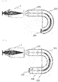
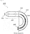
- FIG. 16 is a schematic view of an angle-resolved electron spectrometer developed based on the former idea.
- the basic part of the angle-resolved electron spectrometer 100 is composed of an input lens 102 that accepts and focuses electrons emitted from the sample 101, a concentric hemispherical analyzer (CHA) 103 composed of an inner sphere and an outer sphere, a slit 104 provided at the entrance of the concentric hemispherical analyzer 103 and a detector 105 provided at the exit of the concentric hemispherical analyzer 103.
- CHA concentric hemispherical analyzer
- microscopic spectrum mode also called Transmission mode or Spatial mode
- Angle-resolved spectrum mode also called Diffraction mode or Angular mode
- Switching between the microscopic spectrum mode and the angle-resolved spectrum mode is performed by the lens voltage.
- the lens voltage is adjusted so that the image plane is at the slit position in the microscopic spectrum mode, while the diffraction plane (angle distribution) is at the slit position in the angle-resolved spectrum mode.
- the angle-resolved spectrum mode at the exit of the concentric hemispherical analyzer 103, energy dispersion is formed in the direction connecting the entrance and exit, and a one-dimensional angular distribution is formed in the direction perpendicular to the energy dispersion.
- the angle range that can be measured at one time depends on the acceptance angle of the input lens.
- the electron spectrometer with the above basic configuration has been developed and sold by several manufacturers and widely used.
- a device using a normal input lens had a problem that spherical aberration is large and it was not possible to measure a wide range of emission angle distribution at one time.
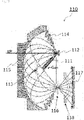
- FIG. 17 is a schematic diagram of a two-dimensional spherical mirror analyzer (DIANA: Display-type Spherical Mirror Analyzer) developed by Daimon et al. (Non-Patent Document 1).
- DIANA Display-type Spherical Mirror Analyzer
- the electrons emitted from the sample 112 by the irradiation of the light from synchrotron radiation (SR) light source or the irradiation of the UV lamp or the electron beam from the electron gun 111 are incident on a spherically symmetric electric field formed between the hemispherical grid 113 and its outer ring-shaped electrodes (114, 115). Then the electrons draw an elliptical orbit in it, and those turning 180° pass through the hemispherical grid 113 again-and focuses to the position of the aperture 116.
- SR synchrotron radiation
- the ring-shaped electrodes (114, 115) are provided with a role of blocking electrons having an energy higher than the path energy, simultaneously with a role of forming a spherically symmetric electric field. Electrons with energies lower than the path energy are reversed in direction due to the spherically symmetric electric field, and some of them pass through the aperture 116. Therefore, a high-pass filter for blocking electrons having an energy lower than the pass energy is provided in front of the screen 117. As shown in FIG. 17 , the high-pass filter is composed of a plurality of grids including the retarding-voltage grid 118.
- DIANA has an acceptance angle of ⁇ 50° or ⁇ 60°, and is characterized in that the two-dimensional emission angle distribution can be measured at once without distortion over the large solid angle. Its ability was demonstrated in the measurement of band dispersion structure using vacuum ultraviolet to soft X-ray light (Non-Patent Documents 2 and 3) and the measurement of atomic arrangement structure (Non-Patent Documents 4 and 5). Here, the set path energy ranges from several 10 eV to 1 keV. For a long time, DIANA was the only analyzer capable of measuring the ⁇ 50° emission angle distribution at one time over this wide energy range.
- DIANA had a problem that the energy resolution is not so good being 0.5% of the path energy.
- Atomic structure analysis such as photoelectron holography and stereoscopic photography of atomic arrangement is performed by setting the kinetic energy of photoelectrons to about 500 to 1000 eV, but in this case, the energy resolution is about several eV to 5 eV. With an energy resolution of several eV to 5 eV, it is difficult to separate and distinguish electronic states with near energy peaks such as chemical shifts and spin-orbit splits.
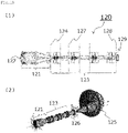
- FIG. 18 shows a schematic diagram of a two-dimensional electron analyzer (DELMA).
- a WAAEL Wide-acceptance-angle electrostatic lens
- An ellipsoidal mesh electrode 122 with a spheroid surface is provided at the entrance of WAAEL, whereby an acceptance angle of ⁇ 45° is achieved.
- the DELMA 120 has a basic portion composed of lenses, and a plurality of Einzel lenses 123 are arranged after the wide-angle electrostatic lens 121 (WAAEL).
- WAAEL wide-angle electrostatic lens
- the energy analysis is performed by inserting the aperture 124 at the exit position of the wide-angle electrostatic lens 121 (WAAEL).
- the possible energy resolution in this case is about 0.3%.
- the measurement is performed in the "microscopic imaging mode" in which the two-dimensional real space image of the sample can be acquired and the "angle distribution mode” in which the two-dimensional emission angle distribution information can be acquired.
- the microscopic imaging mode a magnified image of the sample is projected on the screen of the detector 129, and in the angle distribution mode, a two-dimensional emission angle distribution extending to ⁇ 45° is projected on the screen of the detector 129.
- a magnified image of the sample is observed in the microscopic imaging mode, the region to be examined is aligned with the optical axis, and an aperture (124,127) is inserted for the purpose of field limitation.
- the DELMA is combined with the concentric hemispherical analyzer (CHA) 125 in the same manner as the angle-resolved electron spectrometer shown in FIG. 16 , enabling measurement with high energy resolution.
- the concentric hemispherical analyzer (CHA) 125 is combined so that the sample surface thereof and the detector incident surface 128 of the DELMA 120 coincide with each other.
- the DELMA detector is retracted so that the two-dimensional emission angle distribution is incident on the input lens of the CHA.
- a slit (not shown) at the entrance of the CHA
- a one-dimensional angular distribution in which energy was decomposed can be obtained in the detector (not shown) provided at the exit of the CHA.
- the lens system of the DELMA 120 is provided with an electrostatic deflector 126. With this, it is possible to obtain a two-dimensional emission angle distribution with high energy resolution by inputting electrons into the CHA while scanning the two-dimensional emission angle distribution, acquiring a large number of one-dimensional angle distributions, and combining them.
- the method of obtaining a two-dimensional emission angle distribution by scanning using the electrostatic deflector 126 as described above has also been introduced in the angle-resolved electron spectrometer shown in FIG. 16 , and is now widely used.
- the spherical aberration correction electrostatic lens described in Patent Document 1 and Non-Patent Document 7 is shown in FIGS. 19 ( 1 ) and 19 (2)
- the spherical aberration correction deceleration type lens described in Patent Document 2 and Non-Patent Document 8 is shown in FIGS. 20 ( 1 ) and 20 (2).
- the spherical aberration correction electrostatic lens shown in FIGS. 19 ( 1 ) and 19 (2) is the Einzel lens using an elliptical mesh electrode, and electrons having the same kinetic energy as those emitted from the sample can be obtained at the exit.
- each ellipsoidal mesh electrode is a partial shape of a spheroidal surface whose axis of rotation is the major axis of the ellipsoid.
- the shape occupies about half of the spheroidal surface, and as shown in FIGS.
- the shape occupies more than half of the spheroidal surface. It is difficult to fabricate an ellipsoidal mesh electrode having such a narrow entrance with high definition, high transmittance, and high accuracy. Further, as shown in FIGS. 19 ( 1 ) and 20 (1), even if the ellipsoidal mesh electrode has a mesh shape of about half of the spheroid surface, it is not easy to fabricate a mesh having a large ratio (d/R) of the mesh depth d and the opening radius R of the mesh electrode shown in FIG. 19 (3) with high definition, high transmittance, and high accuracy. In the lenses shown in FIGS. 19 ( 1 ) and 19 (2) and FIGS. 20 ( 1 ) and 20 (2), the ratio (d/R) of the mesh depth d to the opening radius R of the mesh electrode is 1.5 to 2.4.
- the spherical aberration correction electrostatic lens shown in FIG. 19 is used.
- the acceptance angle is set to ⁇ 45°.
- the acceptance angle is designed to be ⁇ 50° or ⁇ 60°, the space around the sample is narrowed, and the incident angle of the irradiation beam irradiating the sample is significantly limited.
- the angle of the irradiation beam from the sample surface is small, the irradiation spot has a shape that extends long in the incident direction. In order to obtain high energy resolution and high sensitivity, it is desirable that the irradiation spot is as small as possible.
- the angle of the irradiation beam from the sample surface is 15°.
- FIG. 21 is a schematic diagram of the parallel beam two-dimensional electron analyzer.
- the basic part of the parallel beam two-dimensional electron analyzer 130 is composed of an ellipsoidal mesh electrode 132, a plurality of axisymmetric electrodes 133a to 133e, a planar collimator electrode 134, and a detector 135.
- the electrons emitted from the sample 131 are taken into the analyzer, parallelized over an acceptance angle of ⁇ 60°, and incident on the planar collimator electrode 134.
- the planar collimator electrode 134 is a plate or thin film having innumerable elongated holes, and when the wall and surface of the pores are coated with an electron absorbing material such as graphite, only electrons with the path energy and electrons in the vicinity of the path energy pass through the planar collimator electrode 134, and other electrons collide with the planar collimator electrode 134 and are absorbed by the electron absorber.
- This enables energy analysis, but the energy resolution and sensitivity are in a trade-off relationship, and if the aspect ratio of the holes in the planar collimator electrode 134 is increased to obtain high energy resolution, there is a problem that a significant decrease in the detection sensitivity is unavoidable.
- FIG. 22 is a schematic configuration diagram of an analyzer in which the PEEM and a high-pass filter are combined (Non-Patent Document 9).
- a magnified image of the sample 142 or a two-dimensional emission angle distribution is projected on the screen 141 of the analyzer 140 depending on the lens voltage.
- Fermi surface mapping can be performed.
- an analyzer that combines a lens system of the PEEM with a concentric hemispherical analyzer has been developed, and it is possible to efficiently perform ARPES (angle-resolved photoelectron spectroscopy) measurement with high energy resolution.
- ARPES angle-resolved photoelectron spectroscopy
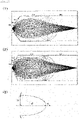
- FIG. 23 is a simple calculation result for explaining this.
- the electron orbit when a uniform accelerating electric field is applied between the sample surface and the entrance of the objective lens is shown.
- the dotted line is a virtual image line taken from the entrance of the objective lens.
- FIG. 23 (1) shows results when the ratio (eUa/E 0 ) of the acceleration voltage Ua multiplied by the elementary charge e to the kinetic energy Eo of the electron on the sample surface is 1000, for example, when Eo is 20 eV for an acceleration voltage of 20 kV.
- the virtual image lines focus to almost one point.
- the emission angle on the sample surface is greatly reduced on the virtual image surface.
- FIG. 23 (2) shows the results when the ratio (eUa/E 0 ) is 10, for example, when E 0 is 2 keV for an acceleration voltage of 20 kV.
- eUa/E 0 10 keV for an acceleration voltage of 20 kV.
- the angle of incidence on the objective lens is significantly increased as compared with the case of FIG. 23 (1).
- a large spherical aberration is occurred even in the objective lens combined with the cathode lens, and the acceptance angle is remarkably reduced.
- the basic part is an input lens that accepts and focuses the electrons emitted from the sample, a concentric hemispherical analyzer consisting of an inner sphere and an outer sphere, a slit provided at the entrance of the concentric hemispherical analyzer, and a detector provided at the exit of the concentric hemispherical analyzer.
- the one-dimensional emission angle distribution that can be measured at one time is determined by the acceptance angle of the input lens.
- the acceptance angle is about ⁇ 10° or less.
- the acceptance angle can be expanded to about ⁇ 50° or ⁇ 60° by using an ellipsoidal mesh, and up to now, spherical aberration correction electrostatic lenses having an acceptance angle of about ⁇ 45° have been developed.
- an acceptance angle of about ⁇ 45° only a region of about 1/4 to 1/3 of the hemispherical solid angle can be captured. Therefore, a larger acceptance angle is desired to measure the emission angle distribution over a wide-angle range in the angle-resolved spectroscopy mode and to improve the sensitivity of the electron spectrometer in the microscopic spectroscopy mode, and ultimately an acceptance angle of ⁇ 90° (omnidirectional acceptance angle) is desired.
- the ratio (d/R) of the mesh depth d of the ellipsoidal mesh and the aperture radius R of the mesh electrode is required about 1.5 to 1.7 in the case of an acceptance angle of ⁇ 50° and is required about 2.0 to 2.4 in the case of an acceptance angle of ⁇ 60°. Since it is not easy to fabricate a mesh having such a shape with high definition, high transmittance, and high accuracy, there is a demand for a means for expanding the acceptance angle without using such an ellipsoidal mesh.
- the analyzer that combines the PEEM and the concentric hemispherical analyzer achieves a large acceptance angle by applying a high voltage between the sample and the entrance of the objective lens and accelerating and accepting the electrons emitted from the sample.
- the acceptance angle decreases significantly with increasing energy, and when the electron kinetic energy E 0 to be analyzed is several 10 eV or less, it is almost ⁇ 90° acceptance angle is achieved, but the acceptance angle drops significantly as the electron kinetic energy Eo increases.
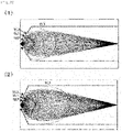
- FIGS. 24 ( 1 ) and 24 (2) are, respectively, the graphs which show the change of the spherical aberration on the virtual image surface and the change of the emergence angle ⁇ , when the acceleration voltage is 20 kV and the kinetic energy of the emitted electrons on the sample surface is changed from 20 eV to 2 keV in the cathode lens shown in FIG. 23 (the horizontal axis is the emission angle ⁇ on the sample surface).
- the lens focusing performance is an important performance that determines the energy resolution and acceptance angle. Even if the spherical aberration of the cathode lens is relatively small, the aberration is magnified by a magnifying lens system provided in the subsequent stage, and the aberration of the lens system itself is added, so that the aberration can be large at the exit of the lens system.
- a slit having a width of about 1 mm or less is inserted at the entrance of the concentric hemispherical analyzer in order to obtain high energy resolution.
- the acceptance angle becomes small.
- the magnification of the input lens used in the concentric hemispherical analyzer is around 5 times.
- the acceptance angle with which it is possible to generate a focused beam by suppressing spherical aberration to a small value is about ⁇ 5° or less.
- the kinetic energy of electrons is at most about 100 to 200 eV in order to achieve an omnidirectional acceptance photoelectron analyzer with high energy resolution using a conventional cathode lens. Further, in the energy region of about 500 eV to 1 keV where atomic structure analysis such as photoelectron diffraction and photoelectron holography is often performed, there is a problem that the acceptance angle is about ⁇ 20° or less.
- the spherical aberration adjustment cathode lens of the present invention is composed of a point source electrode in which a point source is arranged on the lens axis and an extraction electrode for extracting charged particles generated from the point source.
- the point source electrode is one of the following 1a) to 1d
- the extraction electrode is one of the following 2a) and 2b).
- An electrode in which a perforated plate having a through hole on the lens axis or a planar grid is arranged perpendicular to the lens axis.
- An axisymmetric or rod-shaped electrode in which a point source is arranged at the tip, and the tip is arranged at the position of the through hole of a perforated plate having a through hole on the lens axis or through the through hole.
- An electrode has a protruding wall portion with an opening surface formed at the end portion, thereof an inner surface shape is formed axially symmetrically in the axial direction from a base surface, which is perpendicular to the lens axis, wherein a planar grid portion 16 is formed on the opening surface.
- An electrode has a protruding wall portion with an opening surface formed at the end portion, thereof an inner surface shape is formed axially symmetrically in the axial direction from a base surface, which is perpendicular to the lens axis, wherein the opening surface is formed at the end portion where the inner surface shape of the protruding wall portion is tapered outward.
- spherical aberration adjustment cathode lenses of the present invention there are six types of spherical aberration adjustment cathode lenses of the present invention: 1), 2A), 2B), 3A), 3B), and 4) below.
- Point source electrode A planar electrode perpendicular to the lens axis, or an electrode in which a perforated plate having a through hole on the lens axis or a planar grid is arranged perpendicular to the lens axis.
- Extraction electrode An inner surface shape is formed axially symmetrically in the axial direction from the base surface which is perpendicular to the lens axis, and has a protruding wall portion with an opening surface formed at the end portion, and a planar grid is formed on the opening surface.
- Point source electrode A planar electrode perpendicular to the lens axis, having a convex portion axially symmetrical with respect to the lens axis direction in which the point source is arranged in the upper center of the convex portion.
- Extraction electrode An inner surface shape is formed axially symmetrically in the axial direction from the base surface which is perpendicular to the lens axis, and has a protruding wall portion with an opening surface formed at the end portion, and a planar grid is formed on the opening surface.
- Point source electrode An axisymmetric or rod-shaped electrode with a point source located at the tip portion, at the position of a through hole of a perforated plate having the through hole on the lens axis or through the through hole.
- Extraction electrode An inner surface shape is formed axially symmetrically in the axial direction from the base surface which is perpendicular to the lens axis, and has a protruding wall portion with an opening surface formed at the end portion, and a planar grid is formed on the opening surface.
- Point source electrode A planar electrode perpendicular to the lens axis, having a convex portion axially symmetrical with respect to the lens axis direction in which the point source is arranged in the upper center of the convex portion.
- Extraction electrode An inner surface shape is formed axially symmetrically in the axial direction from the base surface which is perpendicular to the lens axis, and has a protruding wall portion with an opening surface formed at the end portion, and the opening surface is formed at the end portion where the inner surface shape of the protrusion wall portion is tapered outward.
- Point source electrode Point source electrode: An axisymmetric or rod-shaped electrode with a point source located at the tip portion, at the position of a through hole of a perforated plate having the through hole on the lens axis or through the through hole.
- Extraction electrode An inner surface shape is formed axially symmetrically in the axial direction from the base surface which is perpendicular to the lens axis, and has a protruding wall portion with an opening surface formed at the end portion, and the opening surface is formed at the end portion where the inner surface shape of the protrusion wall portion is tapered outward.
- Point source electrode A planar electrode perpendicular to the lens axis, or an electrode in which a perforated plate having through holes on the lens axis or a planar grid is arranged perpendicular to the lens axis.
- Extraction electrode An inner surface shape is formed axially symmetrically in the axial direction from the base surface which is perpendicular to the lens axis, and has a protruding wall portion with an opening surface formed at the end portion, and the opening surface is formed at the end portion where the inner surface shape of the protrusion wall portion is tapered outward.
- the protruding wall portion has at least an inner surface shape having a protrusion shape that is axisymmetric from the base surface in the axial direction.
- the perforated plate and the planar grid should be provided with a gas flow path inside or on the surface.
- the extraction electrode preferably has an aspect ratio (h/D) of 0.1 to 0.5 between the height h of the protruding wall portion and the diameter D of the plane grid portion.
- aspect ratio (h/D) approaches 0
- spherical aberration increases remarkably on the wide-angle side.
- the aspect ratio (h/D) approaches 0.6 or more
- a part of the electron orbit on the wide-angle side gets caught on the wall of the protruding wall portion, and the electrons in that orbit cannot pass through the cathode lens.
- the dual-type spherical aberration adjustment cathode lens of the present invention is a cathode lens composed of a point source electrode in which a point source is arranged on the lens axis and an extraction electrode for attracting charged particles generated from the point source.
- the point source electrode has a perforated plate or a planar grid having a through hole on the lens axis arranged perpendicular to the lens axis.
- the extraction electrode has a protruding wall portion in which the inner surface shape is axially symmetrically in the axial direction from a base surface which is perpendicular to the lens axis, and that has an opening surface formed at the end portion thereof, and the first and second electrodes thereof have a planar grid portion formed at the opening surface or an opening surface formed at a tapered protruding wall portion extending from the end portion of the protruding wall portion and expanding outward and at the expanded end portion. Then, the two base surfaces of the first and second electrodes are arranged so as to face each other, and the point source electrode is arranged between the two base surfaces.
- the perforated plate and the planar grid should be provided with a gas flow path inside or on the surface.
- a thin film sample is placed on the lens axis of the perforated plate or the planar grid, or the gas is injected from the side to the through hole on the lens axis and irradiated with light.
- the electrons and ions generated at this time can be detected at a maximum of 4 ⁇ steradian (total solid angle) through the first and second electrodes on the left and right of the point source.
- the extraction electrode has an aspect ratio (h/D) of 0.1 to 0.5 between the height h of the protruding wall portion and the diameter D of the planar grid portion.
- the dual-type spherical aberration adjustment cathode lens of the present invention uses gaseous molecules or particles as the point source, and instead of arranging the perforated plate or the planar grid at the point source electrode, it may be provided with an electric field adjusting means for adjusting the electric field by the applied voltage of the extraction electrode.
- an electric field adjusting means for adjusting the electric field by the applied voltage of the extraction electrode.
- the spherical aberration correction electrostatic lens of the present invention has the spherical aberration adjustment cathode lens of the present invention, a mesh electrode having an axisymmetric concave surface shape facing the protruding wall portion of the extraction electrode, and plural axisymmetric ring-shaped electrodes arranged so that their central axes coincide, and corrects the spherical aberration of the charged particles generated from the point source to generate a focused beam.
- the electrostatic lens is composed in combination of an extraction electrode having a protruding wall portion axisymmetric from the base surface where the lens axis is a perpendicular line, a mesh electrode having an axisymmetric concave surface shape, and a plurality of axisymmetric ring-shaped electrode arranged coaxially.
- the ratio (d/R) of the concave depth d and the opening radius R is 1 or less, and the difficulty in manufacturing the electrode can be reduced.
- the dual-type spherical aberration correction electrostatic lens of the present invention has the dual-type spherical aberration adjustment cathode lens of the present invention, a mesh electrode having an axisymmetric concave surface shape facing the protruding wall portion of each extraction electrode and plural axisymmetric ring-shaped electrodes arranged so that their central axes coincide, and extracts the charged particles generated from the point source and corrects the spherical aberration to generate a focused beam.
- the ratio (d/R) of the concave depth d and the opening radius R is 1 or less, and the difficulty in processing can be reduced.
- the electron spectrometer includes an electrostatic lens of either the spherical aberration correction electrostatic lens of the present invention or the dual-type spherical aberration correction electrostatic lens of the present invention, an axisymmetric deceleration lens arranged coaxially with the electrostatic lens, an aperture arranged at the exit of the deceleration lens, a planar collimator plate is arranged on the exit side of the aperture and arranged co-axis with the electrostatic lens, an axisymmetric mesh electrode that is arranged coaxially with the electrostatic lens to allow charged particles that have passed through the aperture to enter perpendicularly to the planar collimator plate, and a ring-shaped electrode.
- the photoemission electron microscope of the present invention includes an electrostatic lens of either the spherical aberration correction electrostatic lens of the present invention or the dual-type spherical aberration correction electrostatic lens of the present invention, an aperture arranged at the exit of the electrostatic lens, an axisymmetric accelerating lens arranged on the exit side of the aperture and arranged coaxial with the electrostatic lens, a planar collimator plate arranged co-axis with the accelerating lens, an axisymmetric mesh electrode that is arranged coaxially with the electrostatic lens to allow charged particles that have passed through the accelerating lens to enter perpendicularly to the planar collimator plate, and a ring-shaped electrode.
- the angle range that can be measured at one time is one-dimensional, so a projection lens system instead of the above detector and the above detector in the subsequent stage thereof are arranged. Furthermore, by inserting a slit or aperture at the exit of the concentric hemispherical analyzer, it is possible to measure the energy-selected ⁇ 90° two-dimensional emission angle distribution at one time. When an acceptance angle of ⁇ 90° is achieved over a wide energy range, it becomes possible to extract all the information on the band dispersion structure and atomic arrangement structure of photoelectrons. Further, since the sensitivity is generally proportional to the acceptance solid angle, the sensitivity is greatly improved in the spectrum measurement mode.
- the electron spectrometer includes an electrostatic lens of either the spherical aberration correction electrostatic lens of the present invention or the dual-type spherical aberration correction electrostatic lens of the present invention, an axisymmetric deceleration lens arranged coaxial with the electrostatic lens, an aperture arranged at the exit of the deceleration lens, a concentric hemispherical analyzer consisting of inner and outer spheres arranged on the exit side of the aperture.
- the cathode lens of the present invention and the spherical aberration correction electrostatic lens using the same have an effect that ⁇ 90° or a very large acceptance angle can be achieved without using an ellipsoidal mesh with a large ratio (d/R) of the depth d of the mesh electrode and the opening radius R, which is difficult to fabricate with high definition, high transmittance, and high precision. Further, even if the kinetic energy of the electron to be analyzed is as large as several hundred eV or more, which is suitable for atomic structure analysis such as photoelectron holography, it is the effect that ⁇ 90° or a very large acceptance angle can be achieved.
- the acceptance angle of ⁇ 90° can be achieved only when the kinetic energy of electrons is several 10 eV or less, but the spherical aberration correction electrostatic lens of the present invention can achieve the acceptance angle of ⁇ 90° up to at least about 2 keV.
- the spherical aberration correction electrostatic lens of the present invention can accept omnidirectional ( ⁇ 90°) electrons emitted from the sample, correct spherical aberration over all angles, and generate a focused beam with an opening angle of about ⁇ 10° or less.
- the spherical aberration correction electrostatic lens of the present invention can be easily combined with the concentric hemispherical analyzer of the conventional angle-resolved electron spectrometer, and has an effect that a high-energy resolution electron spectrometer with omnidirectional acceptance can be realized in a wide energy range.
- the emission angle distribution over the omnidirectional acceptance angle ( ⁇ 90°) can be measured at once even in a relatively high energy region of about 500 to 1000 eV, which is often used in the measurement of photoelectron diffraction and photoelectron holography.
- the mesh electrode used in the spherical aberration correction electrostatic lens of the present invention can significantly reduce the ratio (d/R) of the mesh depth d to the aperture radius R as compared with the mesh electrode used in the conventional spherical aberration correction electrostatic lens. Specifically, the ratio (d/R) can be reduced to 1.0 or less. This greatly reduces the difficulty of processing the mesh electrode, and makes it possible to manufacture a mesh electrode having high definition, high transmittance, and high accuracy.
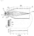
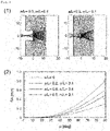
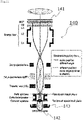
- FIG. 1 shows a schematic diagram of an embodiment 1 of the spherical aberration correction electrostatic lens of the present invention.
- the spherical aberration correction electrostatic lens 1 of the embodiment 1 corresponds to the above-mentioned type 1, and is composed of a point source electrode 12 in which a point source 11 is arranged on the lens axis, an extraction electrode 13 for extracting charged particles generated from the point source 11 in the lens, a mesh electrode 14 having an axisymmetric concave surface shape facing the extraction electrode 13, four axisymmetric ring-shaped electrodes 15a (EL1 to EL4) arranged so that their central axes coincide, and one cylindrical electrode 15b (EL5).
- axisymmetric means that the inner surface shape is axisymmetric.
- a cathode lens 19 is composed of the point source electrode 12 and the extraction electrode 13.
- the point source electrode 12 of the cathode lens 19 is a planar electrode perpendicular to the lens axis
- the extraction electrode 13 has a protruding wall portion 13b in which an inner surface shape is formed axially symmetrically in the axial direction from a base surface 13a, which is perpendicular to the lens axis, and that has an opening surface formed at the end portion thereof, and a planar grid portion 16 is formed at the opening surface of the protruding wall portion 13b.
- the sample is irradiated with light such as ultraviolet rays or X-rays 17, and the electrons emitted from the sample surface are taken in and are focused to the position of the aperture 18. It is also possible to irradiate the sample with an electron beam instead of irradiating with light. However, since the electron beam bends under the action of an electric field even if it is attempted to be irradiated like the irradiation 17 of light, it is desirable to irradiate the electron beam by a method different from that of light.
- a thin film sample is attached to the position of the hole in the point source electrode with the hole on the lens axis, and the electron beam is irradiated from the left side of the figure.
- a method of intaking the electrons appearing on the right side with the spherical aberration correction electrostatic lens is effective.
- a planar grid may be used as the point source electrode, and the thin film sample may be attached on the lens axis.
- gaseous molecules or particles can be used as the sample.
- gaseous molecules or particles can be used as the sample.
- gaseous molecules or the like are injected at the position of the hole of the point source electrode having a through hole.
- gaseous molecules or the like may be injected onto the lens axis of the planar grid.
- the graph shown in FIG. 1 shows SA (Spherical Aberration) with respect to an emission angle ⁇ (-90° to 90°) from the point source in the spherical aberration correction electrostatic lens.
- SA Spherical Aberration
- ⁇ emission angle
- the spherical aberration correction electrostatic lens 1 provided with the cathode lens 19 composed of the point source electrode 12 and the extraction electrode 13 having the above configuration, without using a mesh with a large ratio (d/R) of the depth d of the mesh electrode and the opening radius R (specifically, the mesh with the d/R of about 1.5 or more), an acceptance angle of ⁇ 90° can be achieved.
- the d/R is about 0.90.
- the cathode lens 19 composed of the point source electrode 12 and the extraction electrode 13 will be described with reference to FIGS. 2 and 3 .
- the extraction electrode 13 is characterized by an aspect ratio (h/D) of the height h of the protruding wall portion 13b and the diameter D of the planar grid portion 16.
- the height h is the height of the protruding wall portion 13b protruding in the axial direction from the base surface 13a of the extraction electrode 13 facing the planar point source electrode 12, that is, the height of the planar grid portion from the base surface 13a.
- the extraction electrode does not have a convex shape as shown in FIG. 2 , but may have a protrusion shape whose inner surface shape is axisymmetric.
- the planar point source electrode 12 to which the sample to be the point source 11 is attached is arranged so as to face each other with a certain distance from the extraction electrode 13.
- FIGS. 3 ( 1 ) and 3 (2) are both the results when the kinetic energy of the electrons at the point source 11 is 1 keV and the voltage between the point source electrode 12 and the planar grid portion 16 is 20 kV.
- the kinetic energy of the emitted electrons is set to 1 keV
- the planar point source electrode 12 is set to the ground potential
- the extraction electrode 13 is set to 20 kV
- the four ring-shaped electrodes 15a (EL1 to EL4) and the cylindrical electrode 15b (EL5) are given to the potentials of 20 kV, 10.9 kV, 8.2 kV, 7.2 kV, and 0 V respectively.
- the extraction electrode 13, the mesh electrode 14, and the ring-shaped electrode EL1 have the same potential.
- the point source electrode 12 may be set to an arbitrary potential Vs instead of the ground potential. In this case, each electrode is given a potential obtained by adding Vs to the above potential.
- the distance between the planar point source electrode 12 and the extraction electrode 13 is set to 10 mm, and the aspect ratio h/D (see FIG. 2 ) of the inner surface convex portion of the extraction electrode 13 is set to 0.3.
- the diameter D is 20 mm.
- the voltage applied to each electrode is shown only for the kinetic energy of 1 keV, but in order to correspond to the kinetic energy other than 1 keV, the voltage applied to each electrode may be changed in proportion to the kinetic energy.
- a considerably high voltage is required for the kinetic energy much higher than 1 keV, but if the kinetic energy is about 2 keV, the applied voltage can be about 40 kV at the maximum, which can be handled sufficiently. Further, even in the energy region higher than 2 keV, it may be possible to cope with the region by preparing a suitable high-voltage power supply and designing it with sufficient withstand voltage.
- the application of the lens to the low energy side has no particular problem, changing the applied voltage in proportion to the kinetic energy.
- the kinetic energy is almost zero or very small, in order to avoid the disturbance of the electron orbit due to the disturbance of the surface potential of the electrode member and the influence of geomagnetism, it is desirable to adjust the voltage applied to each electrode so that it converges to the aperture position with a larger kinetic energy than the kinetic energy at the point source.
- the ratio (d/R) of the mesh depth d and the aperture radius R of the elliptical surface mesh electrode is about 1.7.
- the ratio (d/R) is 1.5 to 2.4.
- the ratio (d/R) in the electrostatic lens shown in FIG. 1 is considerably smaller than these ratios.
- the difficulty of processing the mesh electrode is greatly reduced, and it is possible to fabricate the mesh electrode with higher accuracy.
- the aspect ratio (h/D) of the extraction electrode 13 of the spherical aberration correction electrostatic lens of this embodiment is set to 0 (zero)
- the planar grid portion 16 of the extraction electrode 13 and the base surface 13a become flush with each other.
- a uniform electric field is formed between the planar point source electrode 12 to which the sample is attached and the extraction electrode 13.
- spherical aberration will increase significantly on the wide-angle side as compared to the graph shown in FIG. 1 . Therefore, it is desirable to adjust the aspect ratio in order to obtain high focusing performance.
- the aspect ratio is set to 0 there is an advantage that some axis deviation is allowed if the axis is not tilted.
- ring-shaped electrodes EL2 to EL4 arranged after the ring-shaped electrode EL1 to which the mesh electrode 14 is attached, and one cylindrical shape electrode 15b (EL5) further arranged after the ring-shaped electrode are combined.
- the number of electrodes to be combined is not limited to this.
- the spherical aberration correction electrostatic lens of the present invention can be designed as an "omnidirectional acceptance spherical aberration correction electrostatic lens" having an acceptance angle of ⁇ 90° in the energy range of at least 0 to 2 keV.
- omnidirectional acceptance may not be possible. Therefore, unless otherwise specified, the spherical aberration correction electrostatic lens of the present invention represents the electrostatic lens having an omnidirectional or very large acceptance angle.
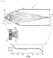
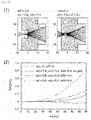
- FIG. 4 shows a schematic diagram of an embodiment 2 of the spherical aberration correction electrostatic lens of the present invention.
- the spherical aberration correction electrostatic lens 2 of the embodiment 2 corresponds to the above-mentioned type 2A, and is composed of a point source electrode 22 in which a point source is arranged on the lens axis, the extraction electrode 13 for extracting charged particles generated from the point source, the mesh electrode 14 having an axisymmetric concave surface shape facing the extraction electrode 13, four axisymmetric ring-shaped electrodes (EL1 to EL4) arranged so that their central axes coincide, and one cylindrical electrode (EL5).
- a point source electrode 22 in which a point source is arranged on the lens axis
- the extraction electrode 13 for extracting charged particles generated from the point source
- the mesh electrode 14 having an axisymmetric concave surface shape facing the extraction electrode 13, four axisymmetric ring-shaped electrodes (EL1 to EL4) arranged so that their central axes coincide, and one cylindrical electrode (EL5)
- a cathode lens 29 has the point source electrode 22 which is a planar electrode perpendicular to the lens axis that has a convex portion axially symmetric in the lens axis direction and has a point source arranged in the center of the upper part of the convex portion.
- the cathode lens 29 has the protruding wall portion 13b in which the inner surface shape is formed in the axial direction axially symmetrically from the base surface 13a perpendicular to the lens axis and in which the opening surface is formed at the end portion, and the extraction electrode 13 in which the planar grid portion 16 is formed at the opening surface of the protruding wall portion 13b.
- the point source electrode 22 is arranged on the concave side of the inner surface of the extraction electrode 13 so as to face each other with a certain distance from the extraction electrode.
- the spherical aberration correction electrostatic lens 2 electrons emitted from the sample surface by irradiation with light such as ultraviolet rays or X-rays are taken over the acceptance angle of ⁇ 90° and a focused beam is generated at the position of the aperture 18, with spherical aberration corrected to be small, by adjusting the shape, arrangement, and applied voltage of each electrode.
- the point source electrode is an axisymmetric electrode in which the point source is arranged at the tip, or a rod-shaped electrode in which the point source is arranged at the tip, and the tip may be arranged at the position of the through hole of the perforated plate having the through hole on the lens axis, or through the through hole.
- This makes it possible to finely adjust the position of the point source in the lens axis direction.
- the axisymmetric electrode in which the point source is arranged at the tip portion and the perforated plate having a through hole on the lens axis do not necessarily have to have the same potential.
- the electric field on the surface of the sample becomes non-uniform due to charging, which may greatly affect the measurement result, but this can be eliminated by applying a bias voltage to the sample.
- a thin straight-shaped electrode that is not axisymmetric is also allowed.
- the graph shown in FIG. 4 shows the spherical aberration SA with respect to the emission angle ⁇ (-90° to 90°) from the point source in the spherical aberration correction electrostatic lens 2.
- the spherical aberration correction electrostatic lens 2 provided with the cathode lens 29 composed of the point source electrode 22 and the extraction electrode 13 having the above configuration, it can be seen that the acceptance angle of ⁇ 90° can be achieved without using a mesh having a large ratio (d/R) of the depth d of the mesh electrode and the opening radius R.
- the ratio (d/R) is about 0.96.
- the spherical aberration correction electrostatic lens 2 makes it possible to make spherical aberration almost zero over incident angles up to ⁇ 90°.
- FIG. 5 shows a schematic diagram of an embodiment 3 of the spherical aberration correction electrostatic lens of the present invention.
- the spherical aberration correction electrostatic lens 3 of the embodiment 3 corresponds to the above-mentioned type 3A, and is composed of the point source electrode 22 in which the point source is arranged on the lens axis, the extraction electrode 33 for extracting charged particles generated from the point source, the mesh electrode 14 having an axisymmetric concave surface shape facing the extraction electrode 33, four axisymmetric ring-shaped electrodes (EL1 to EL4) arranged so that their central axes coincide, and one cylindrical electrode (EL5).
- a cathode lens 39 has the point source electrode 22 which is a planar electrode perpendicular to the lens axis that has a convex portion axially symmetric in the lens axis direction and has a point source arranged in the center of the upper part of the convex portion.
- the cathode lens 39 has the protruding wall portion 33b in which the inner surface shape is formed in the axial direction axially symmetrically from the base surface 33a perpendicular to the lens axis, and the extraction electrode 33 in which a tapered protruding wall portion 33c is formed, which extends from the end of the protruding wall portion 33b and extends outward (the inner surface shape of the protruding wall portion expands outward in a tapered shape).
- the point source electrode 22 is arranged on the concave side of the inner surface of the extraction electrode 33 so as to face each other with a certain distance from the extraction electrode.
- a high voltage applied between the point source electrode 22 and the extraction electrode electrons emitted from the sample are taken in.
- the spherical aberration correction electrostatic lens 3 electrons emitted from the sample surface by irradiation with light such as ultraviolet rays or X-rays are taken over the acceptance angle of ⁇ 90° and a focused beam is generated at the position of the aperture 18, with spherical aberration corrected to be small, by adjusting the shape, arrangement, and applied voltage of each electrode.
- the point source electrode is an axisymmetric electrode in which the point source is arranged at the tip, or a rod-shaped electrode in which the point source is arranged at the tip, and the tip may be arranged at the position of the through hole of the perforated plate having the through hole on the lens axis, or through the through hole.
- This makes it possible to finely adjust the position of the point source in the lens axis direction.
- the axisymmetric electrode in which the point source is arranged at the tip portion and the perforated plate having a through hole on the lens axis do not necessarily have to have the same potential.
- a thin straight-shaped electrode that is not axisymmetric is also allowed.
- the graph shown in FIG. 5 shows the spherical aberration SA with respect to the emission angle ⁇ (-90° to 90°) from the point source in the spherical aberration correction electrostatic lens 3.
- the spherical aberration correction electrostatic lens 3 provided with the cathode lens 39 composed of the point source electrode 22 and the extraction electrode 33 having the above configuration, it can be seen that the acceptance angle of ⁇ 90° can be achieved without using a mesh having a large ratio (d/R) of the depth d of the mesh electrode and the opening radius R.
- the ratio (d/R) is about 0.98.
- the spherical aberration correction electrostatic lens 3 makes it possible to make spherical aberration almost zero over incident angles up to ⁇ 80°.
- FIG. 6 shows a schematic diagram of an embodiment 4 of the spherical aberration correction electrostatic lens of the present invention.
- the spherical aberration correction electrostatic lens 4 of the embodiment 4 corresponds to the above-mentioned type 4, and is composed of the point source electrode 12 in which the point source is arranged on the lens axis, the extraction electrode 33 for extracting charged particles generated from the point source, the mesh electrode 14 having an axisymmetric concave surface shape facing the extraction electrode 33, four axisymmetric ring-shaped electrodes (EL1 to EL4) arranged so that their central axes coincide, and one cylindrical electrode (EL5).
- a cathode lens 49 has the point source electrode 12 which is a planar electrode perpendicular to the lens axis, the protruding wall portion 33b which is formed in the axial direction axially symmetrically from the base surface 33a perpendicular to the lens axis, and the extraction electrode 33 in which a tapered protruding wall portion 33c is formed, which extends outward from the opening surface of the protruding wall portion 33b. Then, the point source electrode 12 is arranged on the concave side of the inner surface of the extraction electrode 33 so as to face each other with a certain distance from the extraction electrode. By a high voltage applied between the point source electrode 12 and the extraction electrode, electrons emitted from the sample are taken in.
- the spherical aberration correction electrostatic lens 4 electrons emitted from the sample surface by irradiation with light such as ultraviolet rays or X-rays are taken over the acceptance angle of ⁇ 90° and a focused beam is generated at the position of the aperture 18, with spherical aberration corrected to be small, by adjusting the shape, arrangement, and applied voltage of each electrode.
- the graph shown in FIG. 6 shows the spherical aberration SA with respect to the emission angle ⁇ (-90° to 90°) from the point source in the spherical aberration correction electrostatic lens 4.
- the spherical aberration correction electrostatic lens 4 provided with the cathode lens 49 composed of the point source electrode 12 and the extraction electrode 33 having the above configuration, it can be seen that a very large acceptance angle can be achieved without using a mesh having a large ratio (d/R) of the depth d of the mesh electrode and the opening radius R.
- the ratio (d/R) is about 0.92.
- the spherical aberration correction electrostatic lens 4 there remains a problem that large spherical aberration occurs when the acceptance angle is about ⁇ 70° or more.
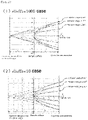
- the results of simulating the effects of the various parameters shown in FIG. 7 are shown below (Distance L between the point source electrode and the base surface of the extraction electrode, Height a of the convex portion of the point source electrode, Radius r 0 of the convex portion of the point source electrode, Height h of the protruding wall portion of the extraction electrode, and Diameter D of the protruding wall portion of the extraction electrode).
- FIGS. 8 to 10 show how the spherical aberration in the virtual image changes due to the change of the above parameters.
- Each figure (2 ) shows the spherical aberration SA (mm) with respect to the emission angle ⁇ (0° to 90°) from the point source.
- FIG. 8 takes into consideration the change in the aspect ratio (h/D) of the protruding wall portion. From this figure, it can be seen that the spherical aberration SA decreases as the aspect ratio (h/D) increases from 0 to 0.5.
- the grid can further reduce the spherical aberration by adjusting the aspect ratio (h/D).
- the upper limit of the aspect ratio (h/D) is about 0.6. This is because when the aspect ratio (h/D) is about 0.6 or more, a part of the electron orbits on the wide-angle side are caught by the wall of the protruding wall portion, and the electrons in those orbits cannot pass through the cathode lens.
- the aspect ratio (h/D) is 0.3. This is the result of optimizing the aspect ratio (h/D) while adjusting various parameters of the mesh electrode, the ring-shaped electrode, and the cylindrical electrode arranged in the subsequent stage of the cathode lens. Further, in the spherical aberration correction electrostatic lens shown in FIG. 6 , the aspect ratio (h/D) is 0.4. However, depending on the design of the mesh electrode, ring-shaped electrode, and cylindrical electrode to be combined with the cathode lens, the optimum aspect ratio (h/D) of the spherical aberration correction electrostatic lens of the present invention can vary within the range of 0.1 to 0.5.
- the size of the diameter D with respect to the distance L between the point source and the base surface of the extraction electrode is determined in the calculation of the optimization of the spherical aberration correction electrostatic lens.
- the D/L is around 2.0.
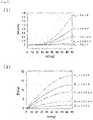
- the effect of the parameter of the convex portion of the point source electrode having the convex portion axisymmetric in the lens axis direction was taken into consideration.
- the parameters are the height a and the radius r 0 of the convex portion shown in FIG. 7 (3). Increasing the height a reduces the spherical aberration, and decreasing the radius r 0 also reduces the spherical aberration. As a result, spherical aberration can be significantly reduced by forming the convex portion into an elongated cylindrical shape. However, in this case, the sample is fixed in a narrow region on the upper surface of the cylinder, which causes a difficulty in practicality.
- FIG. 10 a combination of the parameter of the convex portion of the point source electrode having the convex portion axisymmetric in the lens axial direction and the parameter of the protruding wall portion of the extraction electrode (aspect ratio (h/D)) is considered.
- h/D the parameter of the protruding wall portion of the extraction electrode
- FIGS. 9 ( 1 ) and 10 (1) The electron trajectories (virtual images) for these cases are shown on the left side of FIGS. 9 ( 1 ) and 10 (1).
- spherical aberration can be significantly reduced by combining the point source electrode having an axisymmetric convex portion in the lens axial direction with an extraction electrode having an axisymmetric protruding wall portion. Further, the spherical aberration can be further reduced by reducing the radius r 0 of the convex portion of the point source electrode, and negative spherical aberration can be generated as shown by the alternate long and short dash line in FIG. 10 (2). As shown in FIG.
- the spherical aberration can be considerably adjusted only by the aspect ratio (h/D) of the protruding wall portion of the extraction electrode, but by giving a convex shape to the point source electrode and adding parameters of height a and radius ro, the spherical aberration can be adjusted quite effectively.
- FIGS. 7 (7) and 7 (8) correspond to the above-mentioned types 2B and 3B, respectively.
- FIG. 7 (6) corresponds to the case where the aspect ratio (h/D) of the above-mentioned type 2B is 0.
- the height a of the point source can be finely adjusted to effectively adjust the spherical aberration.
- the point source is arranged not only in the manner in which it is put at the upper center of the convex portion 12a as shown in FIG. 11 (a) , but also in the manner in which it is set at the upper center of the convex portion 12a via the point source support moving device 12b as shown in FIG. 11 (b) or FIG. 11 (c) .
- the point source support moving device 12b is an axisymmetric or rod-shaped electrode in which the point source 11 is arranged at the tip portion, and the tip is arranged at the position of the through hole of the perforated plate having the through hole on the lens axis or at the position through the through hole.
- the sample can be manipulated by using the point source support moving device 12b to finely adjust 12c the position of the point source 11 on the sample.
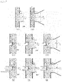
- the electron analyzer of this embodiment is provided with the spherical aberration correction electrostatic lens of the embodiment 1 and an "acceleration / deceleration lens" composed of a plurality of axially symmetric electrodes, in the front stage of the conventional parallel beam two-dimensional electron analyzer.
- the acceleration / deceleration lens is defined as a lens that becomes a deceleration lens or an acceleration lens by switching the voltage.
- emitted electrons are taken in and focused over the omnidirectional acceptance angle ( ⁇ 90°) by the spherical aberration correction electrostatic lens 61 of the present invention, and the two-dimensional emission angle distribution can be measured at one time over the entire angle, with energy being analyzed by the parallel beam two-dimensional electron analyzer 63.
- the acceleration / deceleration lens 62 gives an effect peculiar to this electron analyzer, as will be described later.
- the spherical aberration correction electrostatic lens 61 any of the spherical aberration correction electrostatic lenses shown in the embodiments 1 to 4 may be used.
- FIG. 12 (1) shows a configuration used in the angle distribution mode.
- the acceleration / deceleration lens is used as a "deceleration lens".
- This deceleration lens is used to reduce the kinetic energy before the electrons enter the planar collimator electrode 64 of the parallel beam two-dimensional electron analyzer 63 to improve the energy resolution.
- an insertion-type aperture plate or an iris-type aperture 65 having several holes with different diameters is provided at the exit of the acceleration / deceleration lens 62.
- the aperture 65 and the deceleration lens the energy resolution is improved and sensitivity is adjusted. Deceleration increases the spread of the angle of the electron orbit, which is convenient for the parallel beam two-dimensional electron analyzer 63. The reason is that the larger the incident angle, the higher the energy resolution.
- FIG. 12 (2) shows a configuration used in the imaging mode.
- the imaging mode it is possible to observe a magnified image of the sample and use as a photoemission electron microscope for aligning the region to be examined on the optical axis.
- the acceleration / deceleration lens 62 is used as an "acceleration lens".
- the reason for using the accelerating lens is that the planar collimator electrode 64 is coated with an electron absorbing material in order to block electrons deviated from the parallel beam in the angle distribution mode.
- the angle distribution mode low-energy electrons pass through the planar collimator electrode 64, and the out-of-parallel electrons are absorbed by the electron absorber. While in the imaging mode, a beam close to parallel can be obtained, but a parallel beam as in the angle distribution mode cannot be obtained. Thus, most of the electrons with low energy are absorbed by the electron absorber, and it is difficult to obtain an image.
- the electrons can pass through the planar collimator electrode 64.
- the minute region to be investigated is selected as the analysis region.
- this analyzer can be designed compactly and can be easily combined with other analyzers, so various changes and applications can be expected.
- FIG. 13 is a schematic diagram of a second embodiment of the electron analyzer of the present invention.
- the basic portion of the electron analyzer is composed of an input lens 102, a concentric hemispherical analyzer (CHA) 103 composed of an inner sphere and an outer sphere, and a detector 105 provided at the exit of the concentric hemispherical analyzer 103.
- the spherical aberration correction electrostatic lens 1 of the embodiment 1 is used in the front stage of the input lens arranged in the front stage of the concentric hemispherical analyzer of the electron analyzer.
- the focusing angle of the spherical aberration correction electrostatic lens is important.
- the spherical aberration correction electrostatic lens of the embodiment 1 shown in FIG. 1 is designed to have a focusing angle of ⁇ 10°, but it can also be designed by setting the focusing angle to ⁇ 6°. This solves the electron-loss problem, but if the design has a small focusing angle, the length of the lens will be long. On the contrary, if there is no problem even if the focusing angle is large, the length of the lens can be short.
- the spherical aberration correction electrostatic lens may be designed according to the acceptance angle of the analyzer to be combined.
- the sensitivity in the spectrum mode is roughly proportional to the acceptance solid angle, and the acceptance solid angle is proportional to 1-cos ( ⁇ ) when the acceptance angle is expressed by ⁇ .
- the sensitivity can be expected to be improved by 15 to 18 times.
- the one-dimensional emission angle distribution and energy dispersion in the entire range ( ⁇ 90°) can be measured at the same time.
- the one-dimensional emission angle distribution and energy dispersion in the entire range ( ⁇ 90°) can be measured at the same time.
- the scanning method using the electrostatic deflector described above can be used, and it possible to measure the entire two-dimensional emission angle distribution with high energy resolution in the wide energy range.
- the spherical aberration correction electrostatic lens of any of the embodiments 2 to 4 may be used.
- FIG. 14 is a schematic diagram of a third embodiment of the electron analyzer of the present invention.
- the electron analyzer uses the spherical aberration correction electrostatic lens 1 of the embodiment 1 further before the input lens 102 in the front stage of the concentric hemispherical analyzer composed of the inner sphere and the outer sphere.
- the electron analyzer of the third embodiment is provided with a slit or aperture 104 for energy selection at the exit of the concentric hemispherical analyzer (CHA) 103, and the projection lens 106 and the detector 105 are provided in the subsequent stage.
- CH concentric hemispherical analyzer
- FIG. 15 is a schematic diagram of the dual-type spherical aberration adjustment cathode lens of the present invention.
- the dual-type spherical aberration adjustment cathode lens of the first embodiment is a cathode lens composed of a point source electrode 52 in which the point source is arranged on the lens axis and two extraction electrodes (53a, 53b) for extracting charged particles generated from the point source.
- a perforated plate 51 having a through hole on the lens axis is arranged perpendicular to the lens axis.
- extraction electrodes (53a, 53b) have protruding wall portions (55a, 55b) that are axisymmetric in the axial direction from base surfaces (54a, 54b) whose lens axis are a perpendicular line, and have two left and right first and second electrodes (53a, 53b) in which planar grid portions (56a, 56b) are formed at the opening surface of the protruding wall portion 55, and a point source electrode 52 is arranged in between the two base surfaces (54a, 54b).
- the dual-type spherical aberration adjustment cathode lens of the second embodiment as shown in FIG.
- the point source electrode 52 has a perforated plate 51 having the through hole on the lens axis, and the plate 51 is arranged perpendicular to the lens axis.
- Extraction electrodes (53a, 53b) have protruding wall portions (55a, 55b) that are axisymmetric in the axial direction from base surfaces (54a, 54b) whose lens axis are a perpendicular line, and have two left and right first and second electrodes (53a, 53b) in which tapered protrusions (57a, 57b) extending outward from the opening surface of the protruding wall portions (55a, 55b) are formed, and a point source electrode 52 is arranged in between the two base surfaces (54a, 54b).
- the perforated plate 51 has the through hole 51a in the central portion located on the lens axis, and a thin sample such as graphene is attached, or gas is injected into the through hole 51a on the lens axis, and light is irradiated.
- the perforated plate 51 is provided with a gas flow path 51b inside the plate in order to supply or recover the injected gas. Electrons and ions generated by light irradiation are detected at a maximum of 4 ⁇ steradian (total solid angle) through the left and right electrodes.
- the central electrode allows the formation of a symmetrical potential distribution and the detection of electrons or similar charged particles at both sides.
- the perforated plate 51 can also irradiate electrons instead of the above-mentioned light by providing a path (not shown) through which electrons pass separately from the gas flow path 51b.
- planar grid portions (56a, 56b) of extraction electrodes (53a, 53b) and the base surfaces (54a, 54b) do not have to be symmetrical and may be asymmetric.
- the perforated plate 51 is used for the point source electrode 52 on the lens axis, the planar grid may be used instead of the perforated plate 51.
- the gas flow path may be provided on the plate surface.
- the dual-type spherical aberration adjustment cathode lens can be designed to forma parallel electric field around the point source by the adjusting electric field adjustment means in which the electric field is adjusted by the applied voltage of the extraction electrode, and extract negatively charged particles with one extraction electrode and positively charged particles with the other extraction electrode.
- the electric field adjustment means the parallel electric field is arranged by arranging one or a plurality of ring-shaped electrodes between two opposing extraction electrodes, and a parallel electric field can be easily formed by adjusting the voltage applied to the two extraction electrodes and the ring-shaped electrode.
- the above-mentioned dual-type spherical aberration adjustment cathode lens at the subsequent stage of each extraction electrode, similar the spherical aberration correction electrostatic lens shown in FIG. 1 , is provided a mesh electrode having an axially symmetric concave surface shape facing the extraction electrode, and a plurality of ring-shaped electrodes and one or more cylindrical electrodes arranged so that the central axes coincide with each other, and therefore charged particles generated from the point source are extracted by each extraction electrode, the spherical aberration is corrected, and a focused beam is generated.
- electron analyzers can be designed by arranging the "acceleration / deceleration lens" consisting of a plurality of axisymmetric electrodes, and the parallel beam two-dimensional electron analyzer. This electron analyzer makes it possible to accept and analyze charged particles emitted over 4 ⁇ steradian (omnidirectional acceptance cone angle) with two electrostatic lenses.
- electron analyzers can be designed by arranging the input lens, the concentric hemispherical analyzer consisting of the inner sphere and the outer sphere, and the detector at the exit thereof. Additionally, instead of arranging the detector at the exit of each concentric hemispherical analyzer, the design may be such that a slit or aperture for energy selection is provided, and a projection lens and a detector are provided in the subsequent stage.
- the present invention is useful for electrostatic lenses, electron spectrometers, and photoemission electron microscopes.
Landscapes
- Chemical & Material Sciences (AREA)
- Analytical Chemistry (AREA)
- Analysing Materials By The Use Of Radiation (AREA)
Abstract
Description
- The present invention relates to an electrostatic lens to accept and focus charged particles emitted from a sample by irradiation with light such as ultraviolet rays and X-rays or an electron beam, photoelectron spectroscopy apparatuses such as ultraviolet photoelectron spectroscopy (UPS) and X-ray photoelectron spectroscopy (XPS), an Auger electron spectroscopy apparatus, an angle-resolved photoelectron spectroscopy apparatus, a photoelectron diffraction device, and a photoemission electron microscope.
- In an electron spectrometer, sensitivity is one of the most important performances along with energy resolution. In the measurement of photoelectrons or Auger electrons, when the signal is very weak and almost buried in noise, it is necessary to significantly increase the accumulation time in order to obtain a sufficient signal-to-noise ratio (SN ratio). However, in this case, not only cannot the measurement be performed efficiently, but it is also often the case that the continuous measurement time must be limited due to time constraints such as the utilization time of the synchrotron radiation facility and the duration time of the excitation light source. In addition, in a sample which is susceptible to radiation damage such as an organic material or a sample which is easy to change with time, the measurement is hindered for a long time, and in many cases, a very weak signal is not sufficiently captured.
- It is known that advanced doping techniques are used in the research of new semiconductor materials and superconducting materials, and that even a very small amount of dopant can bring about a great change in the material. Capturing feeble signals from such dopants is extremely important in the development of new materials.
- Further, in the study of micro, nanodevices, polycrystalline materials in which a large number of micro domains are formed, multi-magnetic-domain materials, etc., micro region analysis using a microprobe or a field limiting aperture is important. However, a decrease in signal intensity is unavoidable when trying to measure a smaller area. For these reasons, improving sensitivity is one of the most important points in the development of new electron spectroscopy apparatuses.
- In an electron spectroscopy apparatus, it is possible to measure the emission angle distribution in addition to the measurement of the energy distribution of electrons emitted from a sample. Information on the composition of elements can be obtained by measuring the energy distribution, and information on the composition in the depth direction and electronic state information can be obtained by measuring the emission angle distribution. Further, since the momentum in the in-plane direction of a sample is preserved in the photoelectron emission process, information on the momentum of electrons in the substance can be obtained by measuring the kinetic energy of the photoelectrons and the emission angle. By irradiating the sample with ultraviolet rays or X-rays and measuring the kinetic energy and emission angle distribution of photoelectrons by adjusting the energy to the valence band, it is possible to evaluate the energy band structure of the substance and almost determine the properties of the substance. Furthermore, in the case of photoelectron emission from the inner shell, when the kinetic energy is several hundred eV or more, a strong peak called a forward focusing peak appears in the direction connecting a photoelectron emitting atom and a scatterer atom around it. By measuring this peak over a wide angular range, it becomes possible to directly capture the state of the atomic arrangement around a specific atom. It is also possible to determine the interatomic distance from the diameter of the diffraction ring formed around the forward focusing peak. As mentioned above, the measurement of the emission angle distribution by the electron spectrometer makes it possible to obtain detailed information at the atomic level, which is difficult with other analytical methods. And it will be a very powerful method for developing new materials and researching unknown physical-characteristics expression-mechanism.
- Currently, the emission angle distribution is measured by various methods. In the early days from the 1960s to around 1990, when "high-resolution photoelectron spectroscopy" was established by Kai Siegbahn et al., concentric hemispherical analyzers that accept and analyze only electrons in a specific direction have been widely used. While this concentric hemispherical analyzer can achieve high energy resolution, the measurement of emission angle distribution is performed by rotating the sample or analyzer little by little, so it takes a huge amount of time to acquire data over a wide solid angle. So, it was difficult to measure a wide area of the reciprocal lattice space.
- In addition, "angle-resolved photoelectron spectroscopy" has been developed since around 1990 by two different approaches. One was to introduce new technology in the flow of development of the above "high resolution photoelectron spectroscopy", and the other was to develop a new method focusing on angle distribution measurement.
-
FIG. 16 is a schematic view of an angle-resolved electron spectrometer developed based on the former idea. The basic part of the angle-resolvedelectron spectrometer 100 is composed of aninput lens 102 that accepts and focuses electrons emitted from thesample 101, a concentric hemispherical analyzer (CHA) 103 composed of an inner sphere and an outer sphere, aslit 104 provided at the entrance of the concentrichemispherical analyzer 103 and adetector 105 provided at the exit of the concentrichemispherical analyzer 103. For measurement, "microscopic spectrum mode" (also called Transmission mode or Spatial mode) in which two-dimensional information on the position dependence of the energy spectrum can be obtained at once and "Angle-resolved spectrum mode" (also called Diffraction mode or Angular mode) in which two-dimensional information on the angular distribution of the energy spectrum can be obtained at once are used. - Switching between the microscopic spectrum mode and the angle-resolved spectrum mode is performed by the lens voltage. The lens voltage is adjusted so that the image plane is at the slit position in the microscopic spectrum mode, while the diffraction plane (angle distribution) is at the slit position in the angle-resolved spectrum mode. In the angle-resolved spectrum mode, at the exit of the concentric
hemispherical analyzer 103, energy dispersion is formed in the direction connecting the entrance and exit, and a one-dimensional angular distribution is formed in the direction perpendicular to the energy dispersion. Here, the angle range that can be measured at one time depends on the acceptance angle of the input lens. The electron spectrometer with the above basic configuration has been developed and sold by several manufacturers and widely used. However, a device using a normal input lens had a problem that spherical aberration is large and it was not possible to measure a wide range of emission angle distribution at one time. - On the other hand, as a method focusing on angle-resolved measurement, an electron spectrometer that measures a two-dimensional emission angle distribution at one time has been developed since around 1990.
FIG. 17 is a schematic diagram of a two-dimensional spherical mirror analyzer (DIANA: Display-type Spherical Mirror Analyzer) developed by Daimon et al. (Non-Patent Document 1). In theDIANA 110, the electrons emitted from thesample 112 by the irradiation of the light from synchrotron radiation (SR) light source or the irradiation of the UV lamp or the electron beam from theelectron gun 111 are incident on a spherically symmetric electric field formed between thehemispherical grid 113 and its outer ring-shaped electrodes (114, 115). Then the electrons draw an elliptical orbit in it, and those turning 180° pass through thehemispherical grid 113 again-and focuses to the position of theaperture 116. The ring-shaped electrodes (114, 115) are provided with a role of blocking electrons having an energy higher than the path energy, simultaneously with a role of forming a spherically symmetric electric field. Electrons with energies lower than the path energy are reversed in direction due to the spherically symmetric electric field, and some of them pass through theaperture 116. Therefore, a high-pass filter for blocking electrons having an energy lower than the pass energy is provided in front of thescreen 117. As shown inFIG. 17 , the high-pass filter is composed of a plurality of grids including the retarding-voltage grid 118. Only electrons with path energies and energies in the vicinity can pass through the high-pass filter, and thescreen 117 displays a two-dimensional emission angle distribution with selected energies. DIANA has an acceptance angle of ±50° or ±60°, and is characterized in that the two-dimensional emission angle distribution can be measured at once without distortion over the large solid angle. Its ability was demonstrated in the measurement of band dispersion structure using vacuum ultraviolet to soft X-ray light (Non-Patent Documents 2 and 3) and the measurement of atomic arrangement structure (Non-Patent Documents 4 and 5). Here, the set path energy ranges from several 10 eV to 1 keV. For a long time, DIANA was the only analyzer capable of measuring the ±50° emission angle distribution at one time over this wide energy range. - However, DIANA had a problem that the energy resolution is not so good being 0.5% of the path energy. Atomic structure analysis such as photoelectron holography and stereoscopic photography of atomic arrangement is performed by setting the kinetic energy of photoelectrons to about 500 to 1000 eV, but in this case, the energy resolution is about several eV to 5 eV. With an energy resolution of several eV to 5 eV, it is difficult to separate and distinguish electronic states with near energy peaks such as chemical shifts and spin-orbit splits.
- Therefore, a new two-dimensional electron analyzer (DELMA: Display-type ellipsoidal mesh analyzer) has been developed (Non-Patent Document 6).
FIG. 18 shows a schematic diagram of a two-dimensional electron analyzer (DELMA). A WAAEL (Wide-acceptance-angle electrostatic lens), which is a wide-angleelectrostatic lens 121, has been newly developed for the DELMA 120 and is used as an objective lens. Anellipsoidal mesh electrode 122 with a spheroid surface is provided at the entrance of WAAEL, whereby an acceptance angle of ±45° is achieved. Unlike the DIANA 110 inFIG. 17 , the DELMA 120 has a basic portion composed of lenses, and a plurality ofEinzel lenses 123 are arranged after the wide-angle electrostatic lens 121 (WAAEL). The energy analysis is performed by inserting theaperture 124 at the exit position of the wide-angle electrostatic lens 121 (WAAEL). The possible energy resolution in this case is about 0.3%. - In the
DELMA 120, the measurement is performed in the "microscopic imaging mode" in which the two-dimensional real space image of the sample can be acquired and the "angle distribution mode" in which the two-dimensional emission angle distribution information can be acquired. In the microscopic imaging mode, a magnified image of the sample is projected on the screen of thedetector 129, and in the angle distribution mode, a two-dimensional emission angle distribution extending to ±45° is projected on the screen of thedetector 129. A magnified image of the sample is observed in the microscopic imaging mode, the region to be examined is aligned with the optical axis, and an aperture (124,127) is inserted for the purpose of field limitation. Then, by switching to the angle distribution mode, it becomes possible to measure the two-dimensional emission angle distribution from a specific microscopic region. As shown inFIG. 18 (2), the DELMA is combined with the concentric hemispherical analyzer (CHA) 125 in the same manner as the angle-resolved electron spectrometer shown inFIG. 16 , enabling measurement with high energy resolution. The concentric hemispherical analyzer (CHA) 125 is combined so that the sample surface thereof and thedetector incident surface 128 of theDELMA 120 coincide with each other. For measurements with high energy resolution, the DELMA detector is retracted so that the two-dimensional emission angle distribution is incident on the input lens of the CHA. At this time, by inserting a slit (not shown) at the entrance of the CHA, a one-dimensional angular distribution in which energy was decomposed can be obtained in the detector (not shown) provided at the exit of the CHA. The lens system of theDELMA 120 is provided with anelectrostatic deflector 126. With this, it is possible to obtain a two-dimensional emission angle distribution with high energy resolution by inputting electrons into the CHA while scanning the two-dimensional emission angle distribution, acquiring a large number of one-dimensional angle distributions, and combining them. - The method of obtaining a two-dimensional emission angle distribution by scanning using the
electrostatic deflector 126 as described above has also been introduced in the angle-resolved electron spectrometer shown inFIG. 16 , and is now widely used. - The spherical aberration correction electrostatic lens described in
Patent Document 1 andNon-Patent Document 7 is shown inFIGS. 19 (1 ) and19 (2), and the spherical aberration correction deceleration type lens described inPatent Document 2 andNon-Patent Document 8 is shown inFIGS. 20 (1 ) and20 (2). The spherical aberration correction electrostatic lens shown inFIGS. 19 (1 ) and19 (2) is the Einzel lens using an elliptical mesh electrode, and electrons having the same kinetic energy as those emitted from the sample can be obtained at the exit. The spherical aberration correction deceleration type lens shown inFIGS. 20 (1 ) and20 (2) is a deceleration type lens using an elliptical mesh electrode, and electrons with about 1/5 of the kinetic energy when emitted from the sample are obtained at the exit. As shown inFIGS. 19 (2 ) and20 (2), any of the lenses allows spherical aberration to be corrected over a maximum acceptance angle of ±60°. Each ellipsoidal mesh electrode is a partial shape of a spheroidal surface whose axis of rotation is the major axis of the ellipsoid. As shown inFIGS. 19 (1 ) and20 (1), in the case where the acceptance angle is ±50°, the shape occupies about half of the spheroidal surface, and as shown inFIGS. 19 (2 ) and20 (2), in the case where the acceptance angle is about ±55° to ±60°, the shape occupies more than half of the spheroidal surface. It is difficult to fabricate an ellipsoidal mesh electrode having such a narrow entrance with high definition, high transmittance, and high accuracy. Further, as shown inFIGS. 19 (1 ) and20 (1), even if the ellipsoidal mesh electrode has a mesh shape of about half of the spheroid surface, it is not easy to fabricate a mesh having a large ratio (d/R) of the mesh depth d and the opening radius R of the mesh electrode shown inFIG. 19 (3) with high definition, high transmittance, and high accuracy. In the lenses shown inFIGS. 19 (1 ) and19 (2) andFIGS. 20 (1 ) and20 (2), the ratio (d/R) of the mesh depth d to the opening radius R of the mesh electrode is 1.5 to 2.4. - In the two-dimensional electron analyzer DELMA120 shown in
FIG. 18 , the spherical aberration correction electrostatic lens shown inFIG. 19 is used. However, the acceptance angle is set to ±45°. When the acceptance angle is designed to be ±50° or ±60°, the space around the sample is narrowed, and the incident angle of the irradiation beam irradiating the sample is significantly limited. When the angle of the irradiation beam from the sample surface is small, the irradiation spot has a shape that extends long in the incident direction. In order to obtain high energy resolution and high sensitivity, it is desirable that the irradiation spot is as small as possible. In the DELMA, when the sample is faced to the lens, the angle of the irradiation beam from the sample surface is 15°. - The present inventors have already developed a parallel beam two-dimensional electron analyzer having a wide acceptance angle (see Patent Document 3).
FIG. 21 is a schematic diagram of the parallel beam two-dimensional electron analyzer. The basic part of the parallel beam two-dimensional electron analyzer 130 is composed of anellipsoidal mesh electrode 132, a plurality ofaxisymmetric electrodes 133a to 133e, aplanar collimator electrode 134, and adetector 135. The electrons emitted from thesample 131 are taken into the analyzer, parallelized over an acceptance angle of ±60°, and incident on theplanar collimator electrode 134. Theplanar collimator electrode 134 is a plate or thin film having innumerable elongated holes, and when the wall and surface of the pores are coated with an electron absorbing material such as graphite, only electrons with the path energy and electrons in the vicinity of the path energy pass through theplanar collimator electrode 134, and other electrons collide with theplanar collimator electrode 134 and are absorbed by the electron absorber. This enables energy analysis, but the energy resolution and sensitivity are in a trade-off relationship, and if the aspect ratio of the holes in theplanar collimator electrode 134 is increased to obtain high energy resolution, there is a problem that a significant decrease in the detection sensitivity is unavoidable. - On the other hand, since around 2000, an analyzer that combines a photoemission electron microscope (PEEM) with an energy filter has been developed.
FIG. 22 is a schematic configuration diagram of an analyzer in which the PEEM and a high-pass filter are combined (Non-Patent Document 9). A magnified image of thesample 142 or a two-dimensional emission angle distribution is projected on thescreen 141 of theanalyzer 140 depending on the lens voltage. By using a high-pass filter, Fermi surface mapping can be performed. Furthermore, an analyzer that combines a lens system of the PEEM with a concentric hemispherical analyzer has been developed, and it is possible to efficiently perform ARPES (angle-resolved photoelectron spectroscopy) measurement with high energy resolution. In both of these analyzers and similar analyzers using PEEM technology, a high voltage of several 10 kV is applied between the facingsample 142 and the entrance of theobjective lens 143, and the electrons emitted from the sample are accelerated by a strong accelerating electric field at the same time as the emission and are taken into theobjective lens 143. As a result, a large acceptance angle is achieved. Specifically, for low-energy electrons of several 10 eV or less, an acceptance angle of approximately ±90° is achieved. However, it is difficult to further increase the acceleration voltage from several 10 kV due to problems with the power supply and withstand voltage. As a result, for electrons of several 10 eV or more, there is a problem that the acceptance angle decreases remarkably as the kinetic energy increases. -
FIG. 23 is a simple calculation result for explaining this. The electron orbit when a uniform accelerating electric field is applied between the sample surface and the entrance of the objective lens is shown. The dotted line is a virtual image line taken from the entrance of the objective lens.FIG. 23 (1) shows results when the ratio (eUa/E0) of the acceleration voltage Ua multiplied by the elementary charge e to the kinetic energy Eo of the electron on the sample surface is 1000, for example, when Eo is 20 eV for an acceleration voltage of 20 kV. In this case, it can be seen that the virtual image lines focus to almost one point. Also, it can be seen that the emission angle on the sample surface is greatly reduced on the virtual image surface. As a result, spherical aberration due to the objective lens is significantly reduced, and a very large acceptance angle is achieved.FIG. 23 (2) shows the results when the ratio (eUa/E0) is 10, for example, when E0 is 2 keV for an acceleration voltage of 20 kV. In this case, a large spherical aberration occurs on the virtual image surface. It can also be seen that the angle of incidence on the objective lens is significantly increased as compared with the case ofFIG. 23 (1). As a result, a large spherical aberration is occurred even in the objective lens combined with the cathode lens, and the acceptance angle is remarkably reduced. -
- [Patent Document 1]
JP 4802340 B - [Patent Document 2]
JP 4900389 B - [Patent Document 3]
WO 2017-010529 A1 -
- [Non-Patent Document 1] H. Daimon,"New display-type analyzer for the energy and the angular distribution of charged particles", Rev. Sci. Instrum. 59, 545 (1988).
- [Non-Patent Document 2] F. Matsui, et al., "Three-dimensional band mapping of graphite", Appl. Phys. Lett. 81, 2556 (2002).
- [Non-Patent Document 3] F. Matsui, et al., "Atomic-orbital analysis of the Cu Fermi surface by two-dimensional photoelectron spectroscopy", Phys. Rev. B 72, 195417 (2005).
- [Non-Patent Document 4] F. Matsui, T. Matsushita and H. Daimon, "Stereo atomscope and diffraction spectroscopy--Atomic site specific property analysis", J. Electron Spectrosc. Relat. Phenom. 178-179, 221 (2010).
- [Non-Patent Document 5] F. Matsui, et al., "Selective detection of angular-momentum-polarized Auger electrons by atomic stereography", Phys. Rev. Lett. 114, 015501 (2015).
- [Non-Patent Document 6] H. Matsuda, et al., "Development of display-type ellipsoidal mesh analyzer: Computational evaluation and experimental validation", J. Electron Spectrosc. Relat. Phenom. 195 (2014) 382.
- [Non-Patent Document 7] H. Matsuda, H. Daimon, M. Kato and M. Kudo, "Approach for simultaneous measurement of two-dimensional angular distribution of charged particles: Spherical aberration correction using an ellipsoidal mesh", Phys. Rev. E 71, 066503 (2005).
- [Non-Patent Document 8] H. Matsuda and H. Daimon, "Approach for simultaneous measurement of two-dimensional angular distribution of charged particles. II. Deceleration and focusing of wide-angle beams using a curved mesh lens", Phys. Rev. E 74, 036501 (2006).
- [Non-Patent Document 9] M. Kotsugi et al., "Microspectroscopic two-dimensional Fermi surface mapping using a photoelectron emission microscope", Rev. Sci. Instrum., 74, 2754
- (2003).
- As described above, in the high energy resolution angle-resolved electron spectrometer (see
FIG. 16 ), the basic part is an input lens that accepts and focuses the electrons emitted from the sample, a concentric hemispherical analyzer consisting of an inner sphere and an outer sphere, a slit provided at the entrance of the concentric hemispherical analyzer, and a detector provided at the exit of the concentric hemispherical analyzer. In the angle-resolved spectroscopy mode, the one-dimensional emission angle distribution that can be measured at one time is determined by the acceptance angle of the input lens. In the case of a conventional input lens that does not use a mesh electrode or a grid electrode, the acceptance angle is about ±10° or less. For example, according toPatent Documents - Further, in the spherical aberration correction lenses disclosed in
Patent Documents - On the other hand, the analyzer that combines the PEEM and the concentric hemispherical analyzer achieves a large acceptance angle by applying a high voltage between the sample and the entrance of the objective lens and accelerating and accepting the electrons emitted from the sample. However, when a conventional cathode lens is used in a method of accelerating and accepting electrons as in the PEEM, the acceptance angle decreases significantly with increasing energy, and when the electron kinetic energy E0 to be analyzed is several 10 eV or less, it is almost ±90° acceptance angle is achieved, but the acceptance angle drops significantly as the electron kinetic energy Eo increases.
- This is understood from
FIG. 24. FIGS. 24 (1 ) and24 (2) are, respectively, the graphs which show the change of the spherical aberration on the virtual image surface and the change of the emergence angle β, when the acceleration voltage is 20 kV and the kinetic energy of the emitted electrons on the sample surface is changed from 20 eV to 2 keV in the cathode lens shown inFIG. 23 (the horizontal axis is the emission angle α on the sample surface). - In a high energy resolution analyzer that combines the lens system of the PEEM and the concentric hemispherical analyzer, the lens focusing performance is an important performance that determines the energy resolution and acceptance angle. Even if the spherical aberration of the cathode lens is relatively small, the aberration is magnified by a magnifying lens system provided in the subsequent stage, and the aberration of the lens system itself is added, so that the aberration can be large at the exit of the lens system. A slit having a width of about 1 mm or less is inserted at the entrance of the concentric hemispherical analyzer in order to obtain high energy resolution. Therefore, when a large aberration occurs at the entrance of the concentric hemispherical analyzer, most of the electrons except those having small emission angles on the sample surface are blocked by the slit, and the acceptance angle becomes small. In many cases, the magnification of the input lens used in the concentric hemispherical analyzer is around 5 times. Further, in many input lenses, the acceptance angle with which it is possible to generate a focused beam by suppressing spherical aberration to a small value is about ±5° or less.
- Looking at
FIG. 24 based on such considerations, it can be understood that the kinetic energy of electrons is at most about 100 to 200 eV in order to achieve an omnidirectional acceptance photoelectron analyzer with high energy resolution using a conventional cathode lens. Further, in the energy region of about 500 eV to 1 keV where atomic structure analysis such as photoelectron diffraction and photoelectron holography is often performed, there is a problem that the acceptance angle is about ±20° or less. - In view of such circumstances, it is an object of the present invention to provide a cathode lens a spherical aberration correction electrostatic lens that allow an acceptance angle of approximately ±90° (omnidirectional acceptance angle) or a very large acceptance angle, in a wide energy range ranging from 0 to 2 keV without using a mesh electrode in which the ratio (d/R) of the depth d to the opening radius R is about 1.5 or more, and to provide a high-energy resolution wide-angle electron analyzer using it.
- In order to solve the above problems, the spherical aberration adjustment cathode lens of the present invention is composed of a point source electrode in which a point source is arranged on the lens axis and an extraction electrode for extracting charged particles generated from the point source. In the cathode lens, the point source electrode is one of the following 1a) to 1d), and the extraction electrode is one of the following 2a) and 2b).
- 1a) A planar electrode perpendicular to the lens axis.
- 1b) An electrode in which a planar electrode perpendicular to the lens axis has a convex portion in the lens axis direction that is axisymmetric with respect to the axis, and the point source is arranged in the center of the upper portion of the convex portion.
- 1c) An electrode in which a perforated plate having a through hole on the lens axis or a planar grid is arranged perpendicular to the lens axis.
- 1d) An axisymmetric or rod-shaped electrode in which a point source is arranged at the tip, and the tip is arranged at the position of the through hole of a perforated plate having a through hole on the lens axis or through the through hole.
- 2a) An electrode has a protruding wall portion with an opening surface formed at the end portion, thereof an inner surface shape is formed axially symmetrically in the axial direction from a base surface, which is perpendicular to the lens axis, wherein a
planar grid portion 16 is formed on the opening surface. - 2b) An electrode has a protruding wall portion with an opening surface formed at the end portion, thereof an inner surface shape is formed axially symmetrically in the axial direction from a base surface, which is perpendicular to the lens axis, wherein the opening surface is formed at the end portion where the inner surface shape of the protruding wall portion is tapered outward.
- That is, there are six types of spherical aberration adjustment cathode lenses of the present invention: 1), 2A), 2B), 3A), 3B), and 4) below.
- Point source electrode: A planar electrode perpendicular to the lens axis, or an electrode in which a perforated plate having a through hole on the lens axis or a planar grid is arranged perpendicular to the lens axis.
- Extraction electrode: An inner surface shape is formed axially symmetrically in the axial direction from the base surface which is perpendicular to the lens axis, and has a protruding wall portion with an opening surface formed at the end portion, and a planar grid is formed on the opening surface.
- Point source electrode: A planar electrode perpendicular to the lens axis, having a convex portion axially symmetrical with respect to the lens axis direction in which the point source is arranged in the upper center of the convex portion.
- Extraction electrode: An inner surface shape is formed axially symmetrically in the axial direction from the base surface which is perpendicular to the lens axis, and has a protruding wall portion with an opening surface formed at the end portion, and a planar grid is formed on the opening surface.
- Point source electrode: An axisymmetric or rod-shaped electrode with a point source located at the tip portion, at the position of a through hole of a perforated plate having the through hole on the lens axis or through the through hole.
- Extraction electrode: An inner surface shape is formed axially symmetrically in the axial direction from the base surface which is perpendicular to the lens axis, and has a protruding wall portion with an opening surface formed at the end portion, and a planar grid is formed on the opening surface.
- Point source electrode: A planar electrode perpendicular to the lens axis, having a convex portion axially symmetrical with respect to the lens axis direction in which the point source is arranged in the upper center of the convex portion.
- Extraction electrode: An inner surface shape is formed axially symmetrically in the axial direction from the base surface which is perpendicular to the lens axis, and has a protruding wall portion with an opening surface formed at the end portion, and the opening surface is formed at the end portion where the inner surface shape of the protrusion wall portion is tapered outward.
- Point source electrode: Point source electrode: An axisymmetric or rod-shaped electrode with a point source located at the tip portion, at the position of a through hole of a perforated plate having the through hole on the lens axis or through the through hole.
- Extraction electrode: An inner surface shape is formed axially symmetrically in the axial direction from the base surface which is perpendicular to the lens axis, and has a protruding wall portion with an opening surface formed at the end portion, and the opening surface is formed at the end portion where the inner surface shape of the protrusion wall portion is tapered outward.
- Point source electrode: A planar electrode perpendicular to the lens axis, or an electrode in which a perforated plate having through holes on the lens axis or a planar grid is arranged perpendicular to the lens axis.
- Extraction electrode: An inner surface shape is formed axially symmetrically in the axial direction from the base surface which is perpendicular to the lens axis, and has a protruding wall portion with an opening surface formed at the end portion, and the opening surface is formed at the end portion where the inner surface shape of the protrusion wall portion is tapered outward.
- Here, the protruding wall portion has at least an inner surface shape having a protrusion shape that is axisymmetric from the base surface in the axial direction.
- In the spherical aberration adjustment cathode lens of the present invention, when gaseous molecules or particles are used as a point source, in order to supply or recover the gas to be injected into the through hole on the lens axis, the perforated plate and the planar grid should be provided with a gas flow path inside or on the surface.
- In the spherical aberration adjustment cathode lens of the present invention, the extraction electrode preferably has an aspect ratio (h/D) of 0.1 to 0.5 between the height h of the protruding wall portion and the diameter D of the plane grid portion. When the aspect ratio (h/D) approaches 0, spherical aberration increases remarkably on the wide-angle side. While when the aspect ratio (h/D) approaches 0.6 or more, a part of the electron orbit on the wide-angle side gets caught on the wall of the protruding wall portion, and the electrons in that orbit cannot pass through the cathode lens.
- Further, the dual-type spherical aberration adjustment cathode lens of the present invention is a cathode lens composed of a point source electrode in which a point source is arranged on the lens axis and an extraction electrode for attracting charged particles generated from the point source. In the cathode lens, the point source electrode has a perforated plate or a planar grid having a through hole on the lens axis arranged perpendicular to the lens axis. The extraction electrode has a protruding wall portion in which the inner surface shape is axially symmetrically in the axial direction from a base surface which is perpendicular to the lens axis, and that has an opening surface formed at the end portion thereof, and the first and second electrodes thereof have a planar grid portion formed at the opening surface or an opening surface formed at a tapered protruding wall portion extending from the end portion of the protruding wall portion and expanding outward and at the expanded end portion. Then, the two base surfaces of the first and second electrodes are arranged so as to face each other, and the point source electrode is arranged between the two base surfaces.
- In the dual-type spherical aberration adjustment cathode lens of the present invention, when gaseous molecules or particles are used as the point source, in order to supply or recover the gas to be injected into the through hole on the lens axis, the perforated plate and the planar grid should be provided with a gas flow path inside or on the surface.
- As in the embodiments described later, a thin film sample is placed on the lens axis of the perforated plate or the planar grid, or the gas is injected from the side to the through hole on the lens axis and irradiated with light. The electrons and ions generated at this time can be detected at a maximum of 4π steradian (total solid angle) through the first and second electrodes on the left and right of the point source.
- In the dual-type spherical aberration adjustment cathode lens of the present invention, it is preferable that the extraction electrode has an aspect ratio (h/D) of 0.1 to 0.5 between the height h of the protruding wall portion and the diameter D of the planar grid portion.
- The dual-type spherical aberration adjustment cathode lens of the present invention uses gaseous molecules or particles as the point source, and instead of arranging the perforated plate or the planar grid at the point source electrode, it may be provided with an electric field adjusting means for adjusting the electric field by the applied voltage of the extraction electrode. By this electric field adjusting means, a parallel electric field is formed around the point source, and negatively charged particles are extracted by one extraction electrode and positively charged particles are extracted by the other extraction electrode.
- The spherical aberration correction electrostatic lens of the present invention has the spherical aberration adjustment cathode lens of the present invention, a mesh electrode having an axisymmetric concave surface shape facing the protruding wall portion of the extraction electrode, and plural axisymmetric ring-shaped electrodes arranged so that their central axes coincide, and corrects the spherical aberration of the charged particles generated from the point source to generate a focused beam.
- The electrostatic lens is composed in combination of an extraction electrode having a protruding wall portion axisymmetric from the base surface where the lens axis is a perpendicular line, a mesh electrode having an axisymmetric concave surface shape, and a plurality of axisymmetric ring-shaped electrode arranged coaxially. Here, in the mesh electrode, the ratio (d/R) of the concave depth d and the opening radius R is 1 or less, and the difficulty in manufacturing the electrode can be reduced.
- The dual-type spherical aberration correction electrostatic lens of the present invention has the dual-type spherical aberration adjustment cathode lens of the present invention, a mesh electrode having an axisymmetric concave surface shape facing the protruding wall portion of each extraction electrode and plural axisymmetric ring-shaped electrodes arranged so that their central axes coincide, and extracts the charged particles generated from the point source and corrects the spherical aberration to generate a focused beam. In the mesh electrode, the ratio (d/R) of the concave depth d and the opening radius R is 1 or less, and the difficulty in processing can be reduced.
- The electron spectrometer according to the first aspect of the present invention includes an electrostatic lens of either the spherical aberration correction electrostatic lens of the present invention or the dual-type spherical aberration correction electrostatic lens of the present invention, an axisymmetric deceleration lens arranged coaxially with the electrostatic lens, an aperture arranged at the exit of the deceleration lens, a planar collimator plate is arranged on the exit side of the aperture and arranged co-axis with the electrostatic lens, an axisymmetric mesh electrode that is arranged coaxially with the electrostatic lens to allow charged particles that have passed through the aperture to enter perpendicularly to the planar collimator plate, and a ring-shaped electrode.
- The photoemission electron microscope of the present invention includes an electrostatic lens of either the spherical aberration correction electrostatic lens of the present invention or the dual-type spherical aberration correction electrostatic lens of the present invention, an aperture arranged at the exit of the electrostatic lens, an axisymmetric accelerating lens arranged on the exit side of the aperture and arranged coaxial with the electrostatic lens, a planar collimator plate arranged co-axis with the accelerating lens, an axisymmetric mesh electrode that is arranged coaxially with the electrostatic lens to allow charged particles that have passed through the accelerating lens to enter perpendicularly to the planar collimator plate, and a ring-shaped electrode. However, if a detector is provided at the exit of the concentric hemispherical analyzer, the angle range that can be measured at one time is one-dimensional, so a projection lens system instead of the above detector and the above detector in the subsequent stage thereof are arranged. Furthermore, by inserting a slit or aperture at the exit of the concentric hemispherical analyzer, it is possible to measure the energy-selected ±90° two-dimensional emission angle distribution at one time. When an acceptance angle of ±90° is achieved over a wide energy range, it becomes possible to extract all the information on the band dispersion structure and atomic arrangement structure of photoelectrons. Further, since the sensitivity is generally proportional to the acceptance solid angle, the sensitivity is greatly improved in the spectrum measurement mode.
- The electron spectrometer according to the second aspect of the present invention includes an electrostatic lens of either the spherical aberration correction electrostatic lens of the present invention or the dual-type spherical aberration correction electrostatic lens of the present invention, an axisymmetric deceleration lens arranged coaxial with the electrostatic lens, an aperture arranged at the exit of the deceleration lens, a concentric hemispherical analyzer consisting of inner and outer spheres arranged on the exit side of the aperture.
- The cathode lens of the present invention and the spherical aberration correction electrostatic lens using the same have an effect that ±90° or a very large acceptance angle can be achieved without using an ellipsoidal mesh with a large ratio (d/R) of the depth d of the mesh electrode and the opening radius R, which is difficult to fabricate with high definition, high transmittance, and high precision. Further, even if the kinetic energy of the electron to be analyzed is as large as several hundred eV or more, which is suitable for atomic structure analysis such as photoelectron holography, it is the effect that ±90° or a very large acceptance angle can be achieved.
- In the conventional wide-angle acceptance lens used for PEEM, the acceptance angle of ±90° can be achieved only when the kinetic energy of electrons is several 10 eV or less, but the spherical aberration correction electrostatic lens of the present invention can achieve the acceptance angle of ±90° up to at least about 2 keV. The spherical aberration correction electrostatic lens of the present invention can accept omnidirectional (±90°) electrons emitted from the sample, correct spherical aberration over all angles, and generate a focused beam with an opening angle of about ±10° or less. Further, the spherical aberration correction electrostatic lens of the present invention can be easily combined with the concentric hemispherical analyzer of the conventional angle-resolved electron spectrometer, and has an effect that a high-energy resolution electron spectrometer with omnidirectional acceptance can be realized in a wide energy range. As a result, in the angle distribution mode, the emission angle distribution over the omnidirectional acceptance angle (±90°) can be measured at once even in a relatively high energy region of about 500 to 1000 eV, which is often used in the measurement of photoelectron diffraction and photoelectron holography.
- Further, the mesh electrode used in the spherical aberration correction electrostatic lens of the present invention can significantly reduce the ratio (d/R) of the mesh depth d to the aperture radius R as compared with the mesh electrode used in the conventional spherical aberration correction electrostatic lens. Specifically, the ratio (d/R) can be reduced to 1.0 or less. This greatly reduces the difficulty of processing the mesh electrode, and makes it possible to manufacture a mesh electrode having high definition, high transmittance, and high accuracy.
-
- [
FIG. 1 ] Schematic diagram of the spherical aberration correction electrostatic lens of the present invention (Embodiment 1) . - [
FIG. 2 ] Explanatory view of the spherical aberration correction electrostatic lens. - [
FIG. 3 ] Explanatory view of the cathode lens. - [
FIG. 4 ] Schematic diagram of the spherical aberration correction electrostatic lens of the present invention (Embodiment 2) . - [
FIG. 5 ] Schematic diagram of the spherical aberration correction electrostatic lens of the present invention (Embodiment 3) . - [
FIG. 6 ] Schematic diagram of the spherical aberration correction electrostatic lens of the present invention (Embodiment 4) . - [
FIG. 7 ] Explanatory view of various parameters. - [
FIG. 8 ] Characteristic explanatory view of acceptance angle that changes according to parameters (1). - [
FIG. 9 ] Characteristic explanatory view of acceptance angle that changes according to parameters (2). - [
FIG. 10 ] Characteristic explanatory view of acceptance angle that changes according to parameters (3). - [
FIG. 11 ] Explanatory view of how to arrange the point source in the upper center of the convex portion in the point source electrode. - [
FIG. 12 ] Schematic diagram of a first embodiment of an electron spectrometer in which the spherical aberration correction electrostatic lens of the present invention and a parallel beam generator are combined. - [
FIG. 13 ] Schematic diagram of a second embodiment of an electron spectrometer in which the spherical aberration correction electrostatic lens of the present invention and a concentric hemispherical analyzer are combined. - [
FIG. 14 ] Schematic diagram of a third embodiment of an electron spectrometer in which the spherical aberration correction electrostatic lens of the present invention and a concentric hemispherical analyzer are combined. - [
FIG. 15 ] Explanatory view of the dual-type spherical aberration adjustment cathode lens of the present invention. - [
FIG. 16 ] Schematic diagram of the conventional angle-resolved electron spectrometer. - [
FIG. 17 ] Schematic diagram of the DIANA that is a conventional two-dimensional display type spherical mirror analyzer. - [
FIG. 18 ] Schematic diagram of the DELMA that is a conventional two-dimensional display type ellipsoidal mesh analyzer. - [
FIG. 19 ] Schematic diagram of a conventional spherical aberration correction electrostatic lens. - [
FIG. 20 ] Schematic diagram of a conventional spherical aberration correction / deceleration type lens. - [
FIG. 21 ] Schematic diagram of a conventional parallel beam two-dimensional photoelectron analyzer. - [
FIG. 22 ] Schematic diagram of a photoemission electron microscope PEEM equipped with a conventional energy filter. - [
FIG. 23 ] Schematic diagram of features of a conventional cathode lens used in a conventional PEEM. - [
FIG. 24 ] Schematic diagram of problems of a conventional cathode lens used in a conventional PEEM. - Embodiments of the present invention will be described in detail below with reference to the drawings. The present invention is not limited to the following embodiments and examples of shown in the figure, and the present invention can be variously changed in design.
-
FIG. 1 shows a schematic diagram of anembodiment 1 of the spherical aberration correction electrostatic lens of the present invention. The spherical aberration correctionelectrostatic lens 1 of theembodiment 1 corresponds to the above-mentionedtype 1, and is composed of apoint source electrode 12 in which apoint source 11 is arranged on the lens axis, anextraction electrode 13 for extracting charged particles generated from thepoint source 11 in the lens, amesh electrode 14 having an axisymmetric concave surface shape facing theextraction electrode 13, four axisymmetric ring-shapedelectrodes 15a (EL1 to EL4) arranged so that their central axes coincide, and onecylindrical electrode 15b (EL5). Here, "axisymmetric" means that the inner surface shape is axisymmetric. Acathode lens 19 is composed of thepoint source electrode 12 and theextraction electrode 13. - The point source electrode 12 of the
cathode lens 19 is a planar electrode perpendicular to the lens axis, and theextraction electrode 13 has a protrudingwall portion 13b in which an inner surface shape is formed axially symmetrically in the axial direction from abase surface 13a, which is perpendicular to the lens axis, and that has an opening surface formed at the end portion thereof, and aplanar grid portion 16 is formed at the opening surface of the protrudingwall portion 13b. In the spherical aberration correction electrostatic lens, as shown in the enlarged view in the dotted line frame showing thecathode lens 19, the sample is irradiated with light such as ultraviolet rays orX-rays 17, and the electrons emitted from the sample surface are taken in and are focused to the position of theaperture 18. It is also possible to irradiate the sample with an electron beam instead of irradiating with light. However, since the electron beam bends under the action of an electric field even if it is attempted to be irradiated like theirradiation 17 of light, it is desirable to irradiate the electron beam by a method different from that of light. For example, a thin film sample is attached to the position of the hole in the point source electrode with the hole on the lens axis, and the electron beam is irradiated from the left side of the figure. As a result, a method of intaking the electrons appearing on the right side with the spherical aberration correction electrostatic lens is effective. Here, a planar grid may be used as the point source electrode, and the thin film sample may be attached on the lens axis. Further, instead of the thin film sample, gaseous molecules or particles can be used as the sample. When a sample such as gaseous molecules are used, gaseous molecules or the like are injected at the position of the hole of the point source electrode having a through hole. Alternatively, gaseous molecules or the like may be injected onto the lens axis of the planar grid. - The graph shown in
FIG. 1 shows SA (Spherical Aberration) with respect to an emission angle α (-90° to 90°) from the point source in the spherical aberration correction electrostatic lens. According to the spherical aberration correctionelectrostatic lens 1 provided with thecathode lens 19 composed of thepoint source electrode 12 and theextraction electrode 13 having the above configuration, without using a mesh with a large ratio (d/R) of the depth d of the mesh electrode and the opening radius R (specifically, the mesh with the d/R of about 1.5 or more), an acceptance angle of ±90° can be achieved. In the spherical aberration correction electrostatic lens shown inFIG. 1 , the d/R is about 0.90. - The
cathode lens 19 composed of thepoint source electrode 12 and theextraction electrode 13 will be described with reference toFIGS. 2 and3 . Theextraction electrode 13 is characterized by an aspect ratio (h/D) of the height h of the protrudingwall portion 13b and the diameter D of theplanar grid portion 16. The height h is the height of the protrudingwall portion 13b protruding in the axial direction from thebase surface 13a of theextraction electrode 13 facing the planarpoint source electrode 12, that is, the height of the planar grid portion from thebase surface 13a. In addition, the extraction electrode does not have a convex shape as shown inFIG. 2 , but may have a protrusion shape whose inner surface shape is axisymmetric. - As shown in
FIGS. 2 and3 , at the concave side of the inner surface of theextraction electrode 13 having the protruding wall portion and the planar grid portion formed on the opening surface of the protruding wall portion, the planar point source electrode 12 to which the sample to be thepoint source 11 is attached is arranged so as to face each other with a certain distance from theextraction electrode 13. In the setting where a high voltage is applied between thepoint source electrode 12 and theextraction electrode 13 to accept the electrons emitted from the sample, over the acceptance angle of ±90° by adjusting the shape, arrangement, and applied voltage of each electrode, it is possible to adjust the spherical aberration in the virtual image to a small value over the angle and generate a focused beam in the lens arranged behind the cathode lens. - In addition, as shown in
FIG. 3 (2), the spherical aberration becomes large in the virtual image, when the extraction electrode, facing the planar point source electrode 12 to which the sample to be thepoint source 11 is attached, is without the protrusion wall portion and with only of theplanar grid portion 16.FIGS. 3 (1 ) and3 (2) are both the results when the kinetic energy of the electrons at thepoint source 11 is 1 keV and the voltage between thepoint source electrode 12 and theplanar grid portion 16 is 20 kV. - Here, the calculation conditions of the spherical aberration correction electrostatic lens shown in
FIG. 1 are summarized. The kinetic energy of the emitted electrons is set to 1 keV, the planarpoint source electrode 12 is set to the ground potential, theextraction electrode 13 is set to 20 kV, the four ring-shapedelectrodes 15a (EL1 to EL4) and thecylindrical electrode 15b (EL5) are given to the potentials of 20 kV, 10.9 kV, 8.2 kV, 7.2 kV, and 0 V respectively. Theextraction electrode 13, themesh electrode 14, and the ring-shaped electrode EL1 have the same potential. In addition, thepoint source electrode 12 may be set to an arbitrary potential Vs instead of the ground potential. In this case, each electrode is given a potential obtained by adding Vs to the above potential. - The distance between the planar
point source electrode 12 and theextraction electrode 13 is set to 10 mm, and the aspect ratio h/D (seeFIG. 2 ) of the inner surface convex portion of theextraction electrode 13 is set to 0.3. The diameter D is 20 mm. Assuming that the distance from the origin O to an arbitrary point M of the mesh is ρ and the angle formed by the straight-line OM and the lens axis Z is α, the shape of the mesh electrode is given by the following equation.
[Equation 1]
- Here, b is ρ0-ρ1, pi is the square root of (LM2 + R2), αmax is arctan (R/LM), a1 + a2 + ... + an = 1, LM is the distance from the origin O to the mesh electrode, R is the opening radius of the mesh electrode, and po are the distances from the origin O to the apex T of the mesh. In the electrostatic lens shown in
FIG. 1 , n = 3 is set, and each parameter is given by LM = 37.0 mm, R = 20.0 mm, po = 55.18 mm, a1 = 0.96, a2 = 0.03, and a3 = 0.01. - In the spherical aberration correction electrostatic lens shown in
FIG. 1 , the voltage applied to each electrode is shown only for the kinetic energy of 1 keV, but in order to correspond to the kinetic energy other than 1 keV, the voltage applied to each electrode may be changed in proportion to the kinetic energy. A considerably high voltage is required for the kinetic energy much higher than 1 keV, but if the kinetic energy is about 2 keV, the applied voltage can be about 40 kV at the maximum, which can be handled sufficiently. Further, even in the energy region higher than 2 keV, it may be possible to cope with the region by preparing a suitable high-voltage power supply and designing it with sufficient withstand voltage. - On the other hand, the application of the lens to the low energy side has no particular problem, changing the applied voltage in proportion to the kinetic energy. However, when the kinetic energy is almost zero or very small, in order to avoid the disturbance of the electron orbit due to the disturbance of the surface potential of the electrode member and the influence of geomagnetism, it is desirable to adjust the voltage applied to each electrode so that it converges to the aperture position with a larger kinetic energy than the kinetic energy at the point source.
- By the above method, it is possible to provide a focusing lens having an acceptance angle of ±90° in a wide energy range of at least about 0 to 2 keV. Further, even in the energy region higher than 2 keV, it is possible to provide a focusing lens having an acceptance angle of ±90° if the power supply and withstand voltage resistance allow. Furthermore, even with limited power supply or withstand voltage, optimizing the shape, placement and applied voltage of each electrode may provide the focusing lens with ±90° or a very large acceptance angle.
- In addition, In the case of the spherical aberration correction electrostatic lens used in the two-dimensional electron analyzer (DELMA), the ratio (d/R) of the mesh depth d and the aperture radius R of the elliptical surface mesh electrode is about 1.7. In the case of the spherical aberration correction electrostatic lens described in
Patent Document 1 andNon-Patent Document 7, and the spherical aberration correction deceleration-type lens described inPatent Document 2 andNon-Patent Document 8, the ratio (d/R) is 1.5 to 2.4. As described above, the ratio (d/R) in the electrostatic lens shown inFIG. 1 is considerably smaller than these ratios. In the case of the electrostatic lens shown inFIG. 1 , the difficulty of processing the mesh electrode is greatly reduced, and it is possible to fabricate the mesh electrode with higher accuracy. - When the aspect ratio (h/D) of the
extraction electrode 13 of the spherical aberration correction electrostatic lens of this embodiment is set to 0 (zero), theplanar grid portion 16 of theextraction electrode 13 and thebase surface 13a become flush with each other. As a result, a uniform electric field is formed between the planar point source electrode 12 to which the sample is attached and theextraction electrode 13. When the uniform electric field is formed, spherical aberration will increase significantly on the wide-angle side as compared to the graph shown inFIG. 1 . Therefore, it is desirable to adjust the aspect ratio in order to obtain high focusing performance. However, if the aspect ratio is set to 0, there is an advantage that some axis deviation is allowed if the axis is not tilted. - In the spherical aberration correction electrostatic lens of the present embodiment shown in
FIG. 1 , three ring-shaped electrodes (EL2 to EL4) arranged after the ring-shaped electrode EL1 to which themesh electrode 14 is attached, and onecylindrical shape electrode 15b (EL5) further arranged after the ring-shaped electrode are combined. However, the number of electrodes to be combined is not limited to this. - As described above, the spherical aberration correction electrostatic lens of the present invention can be designed as an "omnidirectional acceptance spherical aberration correction electrostatic lens" having an acceptance angle of ±90° in the energy range of at least 0 to 2 keV. However, depending on the design or energy, omnidirectional acceptance may not be possible. Therefore, unless otherwise specified, the spherical aberration correction electrostatic lens of the present invention represents the electrostatic lens having an omnidirectional or very large acceptance angle.
-
FIG. 4 shows a schematic diagram of anembodiment 2 of the spherical aberration correction electrostatic lens of the present invention. The spherical aberration correctionelectrostatic lens 2 of theembodiment 2 corresponds to the above-mentioned type 2A, and is composed of apoint source electrode 22 in which a point source is arranged on the lens axis, theextraction electrode 13 for extracting charged particles generated from the point source, themesh electrode 14 having an axisymmetric concave surface shape facing theextraction electrode 13, four axisymmetric ring-shaped electrodes (EL1 to EL4) arranged so that their central axes coincide, and one cylindrical electrode (EL5). - As shown in
FIG. 4 , acathode lens 29 has thepoint source electrode 22 which is a planar electrode perpendicular to the lens axis that has a convex portion axially symmetric in the lens axis direction and has a point source arranged in the center of the upper part of the convex portion. Similar to the spherical aberration correctionelectrostatic lens 1 shown inFIG.1 , thecathode lens 29 has the protrudingwall portion 13b in which the inner surface shape is formed in the axial direction axially symmetrically from thebase surface 13a perpendicular to the lens axis and in which the opening surface is formed at the end portion, and theextraction electrode 13 in which theplanar grid portion 16 is formed at the opening surface of the protrudingwall portion 13b. Then, thepoint source electrode 22 is arranged on the concave side of the inner surface of theextraction electrode 13 so as to face each other with a certain distance from the extraction electrode. By a high voltage applied between thepoint source electrode 22 and the extraction electrode, electrons emitted from the sample are taken in. In the spherical aberration correctionelectrostatic lens 2, electrons emitted from the sample surface by irradiation with light such as ultraviolet rays or X-rays are taken over the acceptance angle of ±90° and a focused beam is generated at the position of theaperture 18, with spherical aberration corrected to be small, by adjusting the shape, arrangement, and applied voltage of each electrode. - The point source electrode is an axisymmetric electrode in which the point source is arranged at the tip, or a rod-shaped electrode in which the point source is arranged at the tip, and the tip may be arranged at the position of the through hole of the perforated plate having the through hole on the lens axis, or through the through hole. This makes it possible to finely adjust the position of the point source in the lens axis direction. This corresponds to the above-mentioned type 2B. Here, the axisymmetric electrode in which the point source is arranged at the tip portion and the perforated plate having a through hole on the lens axis do not necessarily have to have the same potential. For example, in the case of an insulator sample, the electric field on the surface of the sample becomes non-uniform due to charging, which may greatly affect the measurement result, but this can be eliminated by applying a bias voltage to the sample. Further, as the rod-shaped electrode, a thin straight-shaped electrode that is not axisymmetric is also allowed.
- The graph shown in
FIG. 4 shows the spherical aberration SA with respect to the emission angle α (-90° to 90°) from the point source in the spherical aberration correctionelectrostatic lens 2. According to the spherical aberration correctionelectrostatic lens 2 provided with thecathode lens 29 composed of thepoint source electrode 22 and theextraction electrode 13 having the above configuration, it can be seen that the acceptance angle of ±90° can be achieved without using a mesh having a large ratio (d/R) of the depth d of the mesh electrode and the opening radius R. In the spherical aberration correctionelectrostatic lens 2, the ratio (d/R) is about 0.96. The spherical aberration correctionelectrostatic lens 2 makes it possible to make spherical aberration almost zero over incident angles up to ±90°. -
FIG. 5 shows a schematic diagram of anembodiment 3 of the spherical aberration correction electrostatic lens of the present invention. The spherical aberration correctionelectrostatic lens 3 of theembodiment 3 corresponds to the above-mentioned type 3A, and is composed of thepoint source electrode 22 in which the point source is arranged on the lens axis, theextraction electrode 33 for extracting charged particles generated from the point source, themesh electrode 14 having an axisymmetric concave surface shape facing theextraction electrode 33, four axisymmetric ring-shaped electrodes (EL1 to EL4) arranged so that their central axes coincide, and one cylindrical electrode (EL5). - A
cathode lens 39 has thepoint source electrode 22 which is a planar electrode perpendicular to the lens axis that has a convex portion axially symmetric in the lens axis direction and has a point source arranged in the center of the upper part of the convex portion. Thecathode lens 39 has the protrudingwall portion 33b in which the inner surface shape is formed in the axial direction axially symmetrically from thebase surface 33a perpendicular to the lens axis, and theextraction electrode 33 in which a tapered protrudingwall portion 33c is formed, which extends from the end of the protrudingwall portion 33b and extends outward (the inner surface shape of the protruding wall portion expands outward in a tapered shape). Then, thepoint source electrode 22 is arranged on the concave side of the inner surface of theextraction electrode 33 so as to face each other with a certain distance from the extraction electrode. By a high voltage applied between thepoint source electrode 22 and the extraction electrode, electrons emitted from the sample are taken in. In the spherical aberration correctionelectrostatic lens 3, electrons emitted from the sample surface by irradiation with light such as ultraviolet rays or X-rays are taken over the acceptance angle of ±90° and a focused beam is generated at the position of theaperture 18, with spherical aberration corrected to be small, by adjusting the shape, arrangement, and applied voltage of each electrode. - The point source electrode is an axisymmetric electrode in which the point source is arranged at the tip, or a rod-shaped electrode in which the point source is arranged at the tip, and the tip may be arranged at the position of the through hole of the perforated plate having the through hole on the lens axis, or through the through hole. This makes it possible to finely adjust the position of the point source in the lens axis direction. This corresponds to the above-mentioned type 3B. Here, as with type 2B, the axisymmetric electrode in which the point source is arranged at the tip portion and the perforated plate having a through hole on the lens axis do not necessarily have to have the same potential. Further, as the rod-shaped electrode with the point source arranged at the tip portion, a thin straight-shaped electrode that is not axisymmetric is also allowed.
- The graph shown in
FIG. 5 shows the spherical aberration SA with respect to the emission angle α (-90° to 90°) from the point source in the spherical aberration correctionelectrostatic lens 3. According to the spherical aberration correctionelectrostatic lens 3 provided with thecathode lens 39 composed of thepoint source electrode 22 and theextraction electrode 33 having the above configuration, it can be seen that the acceptance angle of ±90° can be achieved without using a mesh having a large ratio (d/R) of the depth d of the mesh electrode and the opening radius R. In the spherical aberration correctionelectrostatic lens 3, the ratio (d/R) is about 0.98. The spherical aberration correctionelectrostatic lens 3 makes it possible to make spherical aberration almost zero over incident angles up to ±80°. -
FIG. 6 shows a schematic diagram of anembodiment 4 of the spherical aberration correction electrostatic lens of the present invention. The spherical aberration correctionelectrostatic lens 4 of theembodiment 4 corresponds to the above-mentionedtype 4, and is composed of thepoint source electrode 12 in which the point source is arranged on the lens axis, theextraction electrode 33 for extracting charged particles generated from the point source, themesh electrode 14 having an axisymmetric concave surface shape facing theextraction electrode 33, four axisymmetric ring-shaped electrodes (EL1 to EL4) arranged so that their central axes coincide, and one cylindrical electrode (EL5). - A
cathode lens 49 has thepoint source electrode 12 which is a planar electrode perpendicular to the lens axis, the protrudingwall portion 33b which is formed in the axial direction axially symmetrically from thebase surface 33a perpendicular to the lens axis, and theextraction electrode 33 in which a tapered protrudingwall portion 33c is formed, which extends outward from the opening surface of the protrudingwall portion 33b. Then, thepoint source electrode 12 is arranged on the concave side of the inner surface of theextraction electrode 33 so as to face each other with a certain distance from the extraction electrode. By a high voltage applied between thepoint source electrode 12 and the extraction electrode, electrons emitted from the sample are taken in. In the spherical aberration correctionelectrostatic lens 4, electrons emitted from the sample surface by irradiation with light such as ultraviolet rays or X-rays are taken over the acceptance angle of ±90° and a focused beam is generated at the position of theaperture 18, with spherical aberration corrected to be small, by adjusting the shape, arrangement, and applied voltage of each electrode. - The graph shown in
FIG. 6 shows the spherical aberration SA with respect to the emission angle α (-90° to 90°) from the point source in the spherical aberration correctionelectrostatic lens 4. According to the spherical aberration correctionelectrostatic lens 4 provided with thecathode lens 49 composed of thepoint source electrode 12 and theextraction electrode 33 having the above configuration, it can be seen that a very large acceptance angle can be achieved without using a mesh having a large ratio (d/R) of the depth d of the mesh electrode and the opening radius R. In the spherical aberration correctionelectrostatic lens 4, the ratio (d/R) is about 0.92. However, in the case of the spherical aberration correctionelectrostatic lens 4, there remains a problem that large spherical aberration occurs when the acceptance angle is about ±70° or more. - In the cathode lenses (19, 29, 39, 49) of the spherical aberration correction electrostatic lens of the
embodiments 1 to 4, the results of simulating the effects of the various parameters shown inFIG. 7 are shown below (Distance L between the point source electrode and the base surface of the extraction electrode, Height a of the convex portion of the point source electrode, Radius r0 of the convex portion of the point source electrode, Height h of the protruding wall portion of the extraction electrode, and Diameter D of the protruding wall portion of the extraction electrode). -
FIGS. 8 to 10 show how the spherical aberration in the virtual image changes due to the change of the above parameters. Eachfigure (2 ) shows the spherical aberration SA (mm) with respect to the emission angle α (0° to 90°) from the point source. - In the cathode lens shown in
FIG. 7 (1),FIG. 8 takes into consideration the change in the aspect ratio (h/D) of the protruding wall portion. From this figure, it can be seen that the spherical aberration SA decreases as the aspect ratio (h/D) increases from 0 to 0.5. The alternate long and short dash line shown inFIG. 8 (2) is the result when the aspect ratio (h/D) = 0.4 of the cathode lens shown inFIG. 7 (2) without using the grid. Even when the grid is not used, the spherical aberration is smaller than that in the case of the parallel electric field (when h/D = 0 of the cathode lens inFIG. 7 (1)), but the cathode lens ofFIG. 7 (1) using the grid can further reduce the spherical aberration by adjusting the aspect ratio (h/D). In addition, the upper limit of the aspect ratio (h/D) is about 0.6. This is because when the aspect ratio (h/D) is about 0.6 or more, a part of the electron orbits on the wide-angle side are caught by the wall of the protruding wall portion, and the electrons in those orbits cannot pass through the cathode lens. - In the spherical aberration correction electrostatic lens shown in
FIG. 1 , the aspect ratio (h/D) is 0.3. This is the result of optimizing the aspect ratio (h/D) while adjusting various parameters of the mesh electrode, the ring-shaped electrode, and the cylindrical electrode arranged in the subsequent stage of the cathode lens. Further, in the spherical aberration correction electrostatic lens shown inFIG. 6 , the aspect ratio (h/D) is 0.4. However, depending on the design of the mesh electrode, ring-shaped electrode, and cylindrical electrode to be combined with the cathode lens, the optimum aspect ratio (h/D) of the spherical aberration correction electrostatic lens of the present invention can vary within the range of 0.1 to 0.5. Further, the size of the diameter D with respect to the distance L between the point source and the base surface of the extraction electrode is determined in the calculation of the optimization of the spherical aberration correction electrostatic lens. In the spherical aberration correction electrostatic lenses of theembodiments 1 to 4, the D/L is around 2.0. - In
FIG. 9 , the effect of the parameter of the convex portion of the point source electrode having the convex portion axisymmetric in the lens axis direction was taken into consideration. Here, the parameters are the height a and the radius r0 of the convex portion shown inFIG. 7 (3). Increasing the height a reduces the spherical aberration, and decreasing the radius r0 also reduces the spherical aberration. As a result, spherical aberration can be significantly reduced by forming the convex portion into an elongated cylindrical shape. However, in this case, the sample is fixed in a narrow region on the upper surface of the cylinder, which causes a difficulty in practicality. - Therefore, in
FIG. 10 , a combination of the parameter of the convex portion of the point source electrode having the convex portion axisymmetric in the lens axial direction and the parameter of the protruding wall portion of the extraction electrode (aspect ratio (h/D)) is considered. (Corresponding toFIGS. 7 (4 ) and7 (5)). InFIGS. 9 (2 ) and10 (2), both of the solid line curves are results obtained when the height a and the radius r0 of the convex portion of the point source electrode are set to a/L = 0.6 and r0/L = 0.4, with a and r0 being given as the relative values with respect to the distance L between the point source and the base surface of the extraction electrode. The electron trajectories (virtual images) for these cases are shown on the left side ofFIGS. 9 (1 ) and10 (1). As can be seen from the comparison of these electron trajectories or the comparison of the solid line curves inFIGS. 9 (2 ) and10 (2), spherical aberration can be significantly reduced by combining the point source electrode having an axisymmetric convex portion in the lens axial direction with an extraction electrode having an axisymmetric protruding wall portion. Further, the spherical aberration can be further reduced by reducing the radius r0 of the convex portion of the point source electrode, and negative spherical aberration can be generated as shown by the alternate long and short dash line inFIG. 10 (2). As shown inFIG. 8 , the spherical aberration can be considerably adjusted only by the aspect ratio (h/D) of the protruding wall portion of the extraction electrode, but by giving a convex shape to the point source electrode and adding parameters of height a and radius ro, the spherical aberration can be adjusted quite effectively. - In addition,
FIGS. 7 (7) and 7 (8) correspond to the above-mentioned types 2B and 3B, respectively.FIG. 7 (6) corresponds to the case where the aspect ratio (h/D) of the above-mentioned type 2B is 0. In the above-mentioned types 2B and 3B, the height a of the point source can be finely adjusted to effectively adjust the spherical aberration. - Like the point source electrode in the spherical aberration correction electrostatic lens of the
embodiments FIG. 11 . - The point source is arranged not only in the manner in which it is put at the upper center of the
convex portion 12a as shown inFIG. 11 (a) , but also in the manner in which it is set at the upper center of theconvex portion 12a via the point sourcesupport moving device 12b as shown inFIG. 11 (b) or FIG. 11 (c) . The point sourcesupport moving device 12b is an axisymmetric or rod-shaped electrode in which thepoint source 11 is arranged at the tip portion, and the tip is arranged at the position of the through hole of the perforated plate having the through hole on the lens axis or at the position through the through hole. InFIGS. 11 (b) and 11 (c) , the sample can be manipulated by using the point sourcesupport moving device 12b to finely adjust 12c the position of thepoint source 11 on the sample. - The electron analyzer of this embodiment is provided with the spherical aberration correction electrostatic lens of the
embodiment 1 and an "acceleration / deceleration lens" composed of a plurality of axially symmetric electrodes, in the front stage of the conventional parallel beam two-dimensional electron analyzer. Here, the acceleration / deceleration lens is defined as a lens that becomes a deceleration lens or an acceleration lens by switching the voltage. In the electron analyzer shown inFIG. 12 , emitted electrons are taken in and focused over the omnidirectional acceptance angle (±90°) by the spherical aberration correctionelectrostatic lens 61 of the present invention, and the two-dimensional emission angle distribution can be measured at one time over the entire angle, with energy being analyzed by the parallel beam two-dimensional electron analyzer 63. The acceleration /deceleration lens 62 gives an effect peculiar to this electron analyzer, as will be described later. As the spherical aberration correctionelectrostatic lens 61, any of the spherical aberration correction electrostatic lenses shown in theembodiments 1 to 4 may be used. - First,
FIG. 12 (1) shows a configuration used in the angle distribution mode. In the angle distribution mode, the acceleration / deceleration lens is used as a "deceleration lens". This deceleration lens is used to reduce the kinetic energy before the electrons enter theplanar collimator electrode 64 of the parallel beam two-dimensional electron analyzer 63 to improve the energy resolution. Further, an insertion-type aperture plate or an iris-type aperture 65 having several holes with different diameters is provided at the exit of the acceleration /deceleration lens 62. By theaperture 65 and the deceleration lens, the energy resolution is improved and sensitivity is adjusted. Deceleration increases the spread of the angle of the electron orbit, which is convenient for the parallel beam two-dimensional electron analyzer 63. The reason is that the larger the incident angle, the higher the energy resolution. - Next,
FIG. 12 (2) shows a configuration used in the imaging mode. In the imaging mode, it is possible to observe a magnified image of the sample and use as a photoemission electron microscope for aligning the region to be examined on the optical axis. Here, the acceleration /deceleration lens 62 is used as an "acceleration lens". The reason for using the accelerating lens is that theplanar collimator electrode 64 is coated with an electron absorbing material in order to block electrons deviated from the parallel beam in the angle distribution mode. In the angle distribution mode, low-energy electrons pass through theplanar collimator electrode 64, and the out-of-parallel electrons are absorbed by the electron absorber. While in the imaging mode, a beam close to parallel can be obtained, but a parallel beam as in the angle distribution mode cannot be obtained. Thus, most of the electrons with low energy are absorbed by the electron absorber, and it is difficult to obtain an image. - However, by accelerating the electrons to form an image, the electrons can pass through the
planar collimator electrode 64. After observing the magnified image in the imaging mode and aligning the area to be examined on the optical axis, by inserting theaperture 65 into the exit of the spherical aberration correctionelectrostatic lens 61 for field limitation, the minute region to be investigated is selected as the analysis region. In this state, by setting the angle distribution mode, it is possible to acquire the two-dimensional emission angle distribution of the minute region to be investigated at once over the entire angle. In addition, this analyzer can be designed compactly and can be easily combined with other analyzers, so various changes and applications can be expected. -
FIG. 13 is a schematic diagram of a second embodiment of the electron analyzer of the present invention. As shown inFIG. 13 , the basic portion of the electron analyzer is composed of aninput lens 102, a concentric hemispherical analyzer (CHA) 103 composed of an inner sphere and an outer sphere, and adetector 105 provided at the exit of the concentrichemispherical analyzer 103. In the electron analyzer of the present embodiment, the spherical aberration correctionelectrostatic lens 1 of theembodiment 1 is used in the front stage of the input lens arranged in the front stage of the concentric hemispherical analyzer of the electron analyzer. In the electron analyzer of this embodiment, the focusing angle of the spherical aberration correction electrostatic lens is important. If this focusing angle is larger than the acceptance angle of the input lens, some amount of electron lost occurs with the input lens. Commercial angle-resolved electron spectrometers widely used in basic and applied researches have an acceptance angle of approximately ±6° to ±15°. The spherical aberration correction electrostatic lens of theembodiment 1 shown inFIG. 1 is designed to have a focusing angle of ±10°, but it can also be designed by setting the focusing angle to ±6°. This solves the electron-loss problem, but if the design has a small focusing angle, the length of the lens will be long. On the contrary, if there is no problem even if the focusing angle is large, the length of the lens can be short. - Therefore, in the development of a compact electron analyzer, the spherical aberration correction electrostatic lens may be designed according to the acceptance angle of the analyzer to be combined. The sensitivity in the spectrum mode is roughly proportional to the acceptance solid angle, and the acceptance solid angle is proportional to 1-cos (θ) when the acceptance angle is expressed by ±θ. For that reason, in the electron spectrometer with the acceptance angle of ±6°, by combining an omnidirectional acceptance spherical aberration correction electrostatic lens with a focusing angle set to ±6°, the acceptance solid angle can be magnified by (1 - cos (90°)) / (1 - cos (6°)) = 183 times, and the sensitivity becomes 91 to 110 times multiplied by 0.5 to 0.6, which is the estimated transmittance of the spherical aberration correction electrostatic lens.
- Similarly, if the electron spectrometer having the acceptance angle of ±15° is combined with the spherical aberration correction electrostatic lens of this embodiment, the sensitivity can be expected to be improved by 15 to 18 times. Further, in the angle distribution mode, the one-dimensional emission angle distribution and energy dispersion in the entire range (±90°) can be measured at the same time. Further, in the angle distribution mode, the one-dimensional emission angle distribution and energy dispersion in the entire range (±90°) can be measured at the same time. For the measurement of the two-dimensional emission angle distribution over the omnidirectional acceptance angle (±90°), the scanning method using the electrostatic deflector described above can be used, and it possible to measure the entire two-dimensional emission angle distribution with high energy resolution in the wide energy range. In addition, instead of using the spherical aberration correction electrostatic lens of the
embodiment 1, the spherical aberration correction electrostatic lens of any of theembodiments 2 to 4 may be used. -
FIG. 14 is a schematic diagram of a third embodiment of the electron analyzer of the present invention. As shown inFIG. 14 , similarly to the electron analyzer of the second embodiment shown inFIG. 13 , the electron analyzer uses the spherical aberration correctionelectrostatic lens 1 of theembodiment 1 further before theinput lens 102 in the front stage of the concentric hemispherical analyzer composed of the inner sphere and the outer sphere. Unlike the electron analyzer of the second embodiment shown inFIG. 13 , the electron analyzer of the third embodiment is provided with a slit oraperture 104 for energy selection at the exit of the concentric hemispherical analyzer (CHA) 103, and theprojection lens 106 and thedetector 105 are provided in the subsequent stage. Thereby, it possible to measure a two-dimensional emission angle distribution that has been energy-decomposed with high resolution over the wide energy range at once over the omnidirectional acceptance angle (±90°). -
FIG. 15 is a schematic diagram of the dual-type spherical aberration adjustment cathode lens of the present invention. As shown inFIG. 15 (1), the dual-type spherical aberration adjustment cathode lens of the first embodiment is a cathode lens composed of apoint source electrode 52 in which the point source is arranged on the lens axis and two extraction electrodes (53a, 53b) for extracting charged particles generated from the point source. As thepoint source electrode 52, aperforated plate 51 having a through hole on the lens axis is arranged perpendicular to the lens axis. Further, extraction electrodes (53a, 53b) have protruding wall portions (55a, 55b) that are axisymmetric in the axial direction from base surfaces (54a, 54b) whose lens axis are a perpendicular line, and have two left and right first and second electrodes (53a, 53b) in which planar grid portions (56a, 56b) are formed at the opening surface of the protruding wall portion 55, and apoint source electrode 52 is arranged in between the two base surfaces (54a, 54b). Further, in the dual-type spherical aberration adjustment cathode lens of the second embodiment, as shown inFIG. 15 (2), thepoint source electrode 52 has a perforatedplate 51 having the through hole on the lens axis, and theplate 51 is arranged perpendicular to the lens axis. Extraction electrodes (53a, 53b) have protruding wall portions (55a, 55b) that are axisymmetric in the axial direction from base surfaces (54a, 54b) whose lens axis are a perpendicular line, and have two left and right first and second electrodes (53a, 53b) in which tapered protrusions (57a, 57b) extending outward from the opening surface of the protruding wall portions (55a, 55b) are formed, and apoint source electrode 52 is arranged in between the two base surfaces (54a, 54b). - Here, as shown in
FIG. 15 (3), theperforated plate 51 has the throughhole 51a in the central portion located on the lens axis, and a thin sample such as graphene is attached, or gas is injected into the throughhole 51a on the lens axis, and light is irradiated. Theperforated plate 51 is provided with agas flow path 51b inside the plate in order to supply or recover the injected gas. Electrons and ions generated by light irradiation are detected at a maximum of 4π steradian (total solid angle) through the left and right electrodes. The central electrode allows the formation of a symmetrical potential distribution and the detection of electrons or similar charged particles at both sides. By changing the way the voltage is applied, it is possible to measure the coincidence of positive and negative charged particles at the left and right. Theperforated plate 51 can also irradiate electrons instead of the above-mentioned light by providing a path (not shown) through which electrons pass separately from thegas flow path 51b. - In addition, the distance and the shape of planar grid portions (56a, 56b) of extraction electrodes (53a, 53b) and the base surfaces (54a, 54b) do not have to be symmetrical and may be asymmetric. Further, although the
perforated plate 51 is used for thepoint source electrode 52 on the lens axis, the planar grid may be used instead of theperforated plate 51. Further, instead of providing the gas flow path inside theperforated plate 51, the gas flow path may be provided on the plate surface. - When gaseous molecules or particles are used as the point source, instead of arranging the perforated plate (or the planar grid) as shown in
FIG. 15 , the dual-type spherical aberration adjustment cathode lens can be designed to forma parallel electric field around the point source by the adjusting electric field adjustment means in which the electric field is adjusted by the applied voltage of the extraction electrode, and extract negatively charged particles with one extraction electrode and positively charged particles with the other extraction electrode. Here, as the electric field adjustment means, the parallel electric field is arranged by arranging one or a plurality of ring-shaped electrodes between two opposing extraction electrodes, and a parallel electric field can be easily formed by adjusting the voltage applied to the two extraction electrodes and the ring-shaped electrode. - The above-mentioned dual-type spherical aberration adjustment cathode lens, at the subsequent stage of each extraction electrode, similar the spherical aberration correction electrostatic lens shown in
FIG. 1 , is provided a mesh electrode having an axially symmetric concave surface shape facing the extraction electrode, and a plurality of ring-shaped electrodes and one or more cylindrical electrodes arranged so that the central axes coincide with each other, and therefore charged particles generated from the point source are extracted by each extraction electrode, the spherical aberration is corrected, and a focused beam is generated. - Further, at the subsequent stage of each electrostatic lens of the above-mentioned dual-type spherical aberration correction electrostatic lens, as shown in
FIG. 12 , electron analyzers can be designed by arranging the "acceleration / deceleration lens" consisting of a plurality of axisymmetric electrodes, and the parallel beam two-dimensional electron analyzer. This electron analyzer makes it possible to accept and analyze charged particles emitted over 4π steradian (omnidirectional acceptance cone angle) with two electrostatic lenses. - Further, at the subsequent stage of each electrostatic lens of the above-mentioned dual-type spherical aberration correction electrostatic lens, as shown in
FIG. 13 , electron analyzers can be designed by arranging the input lens, the concentric hemispherical analyzer consisting of the inner sphere and the outer sphere, and the detector at the exit thereof. Additionally, instead of arranging the detector at the exit of each concentric hemispherical analyzer, the design may be such that a slit or aperture for energy selection is provided, and a projection lens and a detector are provided in the subsequent stage. As a result, in a wide energy range, charged particles emitted over 4π steradians (total solid angles) are extracted by each electrostatic lens, it is possible to provide an electron analyzer that measures a two-dimensional emission angle distribution over all solid angles at once with high energy resolution. - The present invention is useful for electrostatic lenses, electron spectrometers, and photoemission electron microscopes.
-
- 1, 2, 3, 4, 61 Spherical aberration correction electrostatic lens
- 11 Point source
- 12, 22, 52 Point source electrode
- 12a Convex portion
- 12b Point source support moving device
- 13, 33, 50, 53a, 53b Extraction electrode
- 13a, 33a, 54a, 54b Base surface
- 13b, 33b, 55a, 55b Protruding wall portion
- 33c, 57a, 57b Tapered protruding wall portion
- 14 Mesh electrode
- 15a Ring-shaped electrode
- 15b Cylindrical electrode
- 16, 56a, 56b Planar grid portion
- 18, 65, 116, 124, 127 Aperture
- 19, 29, 39, 49 Cathode lens
- 51 Perforated plate
- 51a Through hole
- 51b Gas flow path
- 62 Acceleration / deceleration lens
- 63 Parallel beam two-dimensional electron analyzer
- 64 Planar collimator electrode
- 100 Electron spectrometer
- 101, 112, 131, 142 Sample
- 102 Input lens
- 103 Concentric hemispherical analyzer (CHA)
- 104 Slit / aperture
- 105, 135 Detector
- 106 Projection lens
- 110 DIANA
- 111 Electron gun
- 113 Hemispherical grid
- 114, 115 Ring-shaped electrode
- 117, 141 Screen
- 118 Retarding-voltage grid
- 120 DELMA
- 121 Wide-angle electrostatic lens
- 122, 132 Ellipsoidal mesh electrode
- 123 Einzel lens
- 125 Concentric hemispherical analyzer (CHA)
- 126 Electrostatic deflector
- 129 Detector
- 130 Parallel beam two-dimensional electron analyzer
- 133a - 133e Axisymmetric electrode
- 134 Planar collimator electrode
- 140 Analyzer
- 143 Objective lens
Claims (15)
- A spherical aberration adjustment cathode lens comprising:a point source electrode in which a point source is arranged on the lens axis, andan extraction electrode for extracting charged particles generated from the point source,wherein the extraction electrode has a protruding wall portion that forms an inner surface shape axially symmetrically in the axial direction from a base surface, which is perpendicular to the lens axis, and that has an opening surface formed at the end portion thereof, and a planar grid portion is formed at the opening surface, or the opening surface is formed at the end portion where the inner surface shape of the protrusion wall portion is tapered outward.
- The spherical aberration adjustment cathode lens according to claim 1, wherein the point source electrode is any of the following;a) a planar electrode perpendicular to the lens axis, orb) an electrode in which a planar electrode perpendicular to the lens axis has a convex portion that is axisymmetric in the lens axis direction, and the point source is arranged in the center of the upper portion of the convex portion, orc) an axisymmetric or rod-shaped electrode in which a point source is arranged at the tip, and the tip is arranged at the position of the through hole of a perforated plate having a through hole on the lens axis or through the through hole.
- The spherical aberration adjustment cathode lens according to claim 1, wherein the extraction electrodes are first and second extraction electrodes arranged so that the base surfaces face each other, and are dual-type in which the point source electrode is arranged between two base surfaces.
- The spherical aberration adjustment cathode lens according to claim 1, wherein the point source electrode is a perforated plate having a through hole on the lens axis or a planar grid arranged perpendicular to the lens axis, using gaseous molecules or particles as the point source, in order to supply or recover the gas to be injected into the through hole on the lens axis, the perforated plate and the planar grid are provided with a gas flow path inside or on the surface.
- The spherical aberration adjustment cathode lens according to claim 3, wherein the point source electrode is a perforated plate having a through hole on the lens axis or a planar grid arranged perpendicular to the lens axis, using gaseous molecules or particles as the point source, in order to supply or recover the gas to be injected into the through hole on the lens axis, the perforated plate and the planar grid are provided with a gas flow path inside or on the surface.
- The spherical aberration adjustment cathode lens according to any one of claims 1, 2 and 4, wherein the extraction electrode has an aspect ratio (h/D) of 0.1 to 0.5 between the height h of the protruding wall portion and the diameter D of the planar grid portion.
- The spherical aberration adjustment cathode lens according to claim 3 or 5, wherein the extraction electrode has an aspect ratio (h/D) of 0.1 to 0.5 between the height h of the protruding wall portion and the diameter D of the planar grid portion.
- The spherical aberration adjustment cathode lens according to any one of claims 3, 5 and 7, wherein gaseous molecules or particles are used as the point source, and instead of arranging the perforated plate or the planar grid in the point source electrode, an electric field adjustment means for adjusting the electric field by the applied voltage of the extraction electrode, and thereby a parallel electric field is formed around the point source, negatively charged particles are extracted by one of the extraction electrode, and positively charged particles are extracted by the other extraction electrode.
- A spherical aberration correction electrostatic lens comprising:the spherical aberration adjustment cathode lens according to any one of claims 1, 2, 4 and 6, anda mesh electrode having an axisymmetric concave surface shape facing the protruding wall portion of the extraction electrode, andplural axisymmetric ring-shaped electrodes arranged so that the central axes coincide, and which corrects the spherical aberration of charged particles generated from the point source and generates a focused beam.
- A dual-type spherical aberration correction electrostatic lens comprising:the spherical aberration adjustment cathode lens according to any one of claims 3, 5, 7 and 8, anda mesh electrode having an axisymmetric concave surface shape facing the protruding wall portion, andplural axisymmetric ring-shaped electrodes arranged so that the central axes coincide, and which extracts charged particles generated from the point source at each of the extraction electrodes, corrects the spherical aberration and generates a focused beam.
- The spherical aberration correction electrostatic lens according to claim 9, wherein the ratio (d/R) of the depth d of the concave surface to the opening radius R is 1 or less in the mesh electrode.
- The dual-type spherical aberration correction electrostatic lens according to claim 10, wherein the ratio (d/R) of the depth d of the concave surface to the opening radius R is 1 or less in the mesh electrode.
- An electron spectrometer comprising:the electrostatic lens of either the spherical aberration correction electrostatic lens according to claim 9 or 11, or the dual-type spherical aberration correction electrostatic lens according to claim 10 or 12;an axisymmetric deceleration lens arranged coaxially with the electrostatic lens;an aperture arranged at the exit of the deceleration lens; andaxisymmetric mesh electrodes and ring-shaped electrodes arranged coaxially with the electrostatic lens so that charged particles that have passed through the aperture are vertically incident on the planar collimator plate.
- A photoemission electron microscope comprising:the electrostatic lens of either the spherical aberration correction electrostatic lens according to claim 9 or 11, or the dual-type spherical aberration correction electrostatic lens according to claim 10 or 12;an aperture arranged at the exit of the electrostatic lens;an axisymmetric accelerating lens arranged on the exit side of the aperture and coaxially arranged with the electrostatic lens;a planar collimator plate arranged on the same axis as the acceleration lens; andaxisymmetric mesh electrodes and ring-shaped electrodes arranged coaxially with the electrostatic lens so that charged particles that have passed through the acceleration lens are vertically incident on the planar collimator plate.
- An electron spectrometer comprising:the electrostatic lens of either the spherical aberration correction electrostatic lens according to claim 9 or 11, or the dual-type spherical aberration correction electrostatic lens according to claim 10 or 12;
an axisymmetric deceleration lens coaxially arranged with the electrostatic lens;an aperture arranged at the exit of the electrostatic lens; anda concentric hemispherical analyzer which is arranged on the exit side of the aperture and consists of inner and outer spheres.
Applications Claiming Priority (2)
| Application Number | Priority Date | Filing Date | Title |
|---|---|---|---|
| JP2019227788 | 2019-12-17 | ||
| PCT/JP2020/047288 WO2021125297A1 (en) | 2019-12-17 | 2020-12-17 | Spherical aberration adjustment cathode lens, spherical aberration correction electrostatic lens, electron spectroscope, and photoemission electron microscope |
Publications (2)
| Publication Number | Publication Date |
|---|---|
| EP4075475A1 true EP4075475A1 (en) | 2022-10-19 |
| EP4075475A4 EP4075475A4 (en) | 2024-07-24 |
Family
ID=76476761
Family Applications (1)
| Application Number | Title | Priority Date | Filing Date |
|---|---|---|---|
| EP20903239.0A Pending EP4075475A4 (en) | 2019-12-17 | 2020-12-17 | SPHERICAL ABERRATION ADJUSTMENT CATHODE LENS, SPHERICAL ABERRATION CORRECTION ELECTROSTATIC LENS, ELECTRON SPECTROSCOPE AND PHOTOEMISSION ELECTRON MICROSCOPE |
Country Status (3)
| Country | Link |
|---|---|
| EP (1) | EP4075475A4 (en) |
| JP (1) | JP7505794B2 (en) |
| WO (1) | WO2021125297A1 (en) |
Families Citing this family (1)
| Publication number | Priority date | Publication date | Assignee | Title |
|---|---|---|---|---|
| US20240047190A1 (en) | 2020-07-09 | 2024-02-08 | Inter-University Research Institute Corporation National Institute Of Natural Sciences | Electrostatic deflection convergence-type energy analyzer, imaging-type electron spectroscopic device, reflecting imaging-type electron spectroscopic device, and spin vector distribution imaging device |
Family Cites Families (8)
| Publication number | Priority date | Publication date | Assignee | Title |
|---|---|---|---|---|
| JP2556833B2 (en) * | 1986-01-31 | 1996-11-27 | 株式会社島津製作所 | Photoelectron spectroscopy analyzer |
| JP3347491B2 (en) * | 1994-10-12 | 2002-11-20 | 日本電子株式会社 | Spherical aberration correction electrostatic lens |
| GB9718012D0 (en) * | 1997-08-26 | 1997-10-29 | Vg Systems Ltd | A spectrometer and method of spectroscopy |
| WO2006008840A1 (en) * | 2004-07-15 | 2006-01-26 | National University Corporation NARA Institute of Science and Technology | Spherical aberration correction electrostatic lens, input lens, electron spectroscopic device, photoelectron microscope, and measurement system |
| JP2006324119A (en) | 2005-05-19 | 2006-11-30 | Hitachi Ltd | Electron gun |
| EP2058834B1 (en) | 2006-07-26 | 2015-12-09 | National University Corporation Nara Institute of Science and Technology | Spherical aberration correction decelerating lens, spherical aberration correction lens system, electron spectroscopy device, and photoelectron microscope |
| WO2012126792A1 (en) * | 2011-03-18 | 2012-09-27 | Ecole Polytechnique Federale De Lausanne (Epfl) | Electron beam apparatus |
| EP3324421A4 (en) | 2015-07-15 | 2019-04-24 | National University corporation Nara Institute of Science and Technology | ELECTROSTATIC LENS, AND PARALLEL BEAM GENERATING DEVICE, AND PARALLEL BEAM CONVERGENCE DEVICE USING THE ELECTROSTATIC LENS AND A COLLIMATOR |
-
2020
- 2020-12-17 JP JP2021565660A patent/JP7505794B2/en active Active
- 2020-12-17 WO PCT/JP2020/047288 patent/WO2021125297A1/en not_active Ceased
- 2020-12-17 EP EP20903239.0A patent/EP4075475A4/en active Pending
Also Published As
| Publication number | Publication date |
|---|---|
| WO2021125297A1 (en) | 2021-06-24 |
| EP4075475A4 (en) | 2024-07-24 |
| JP7505794B2 (en) | 2024-06-25 |
| JPWO2021125297A1 (en) | 2021-06-24 |
Similar Documents
| Publication | Publication Date | Title |
|---|---|---|
| Liebl | Ion microprobe mass analyzer | |
| Reimer | Transmission electron microscopy: physics of image formation and microanalysis | |
| JP6151138B2 (en) | Method for performing tomographic imaging of a sample in a charged particle microscope | |
| EP0246841B1 (en) | Electron spectrometer | |
| Khursheed | Scanning electron microscope optics and spectrometers | |
| US8013298B2 (en) | Electrostatic electron spectrometry apparatus | |
| US4740694A (en) | Method and apparatus for analyzing positron extinction and electron microscope having said apparatus | |
| JP6757036B2 (en) | Electrostatic lens, parallel beam generator and parallel beam converging device using the lens and collimator | |
| CN112305002B (en) | Spectroscopy and imaging system | |
| KR20160005042A (en) | Leed for sem | |
| JP4444494B2 (en) | Electron detector | |
| US11791148B2 (en) | Variable reduction ratio spherical aberration correction electrostatic lens, wide angle energy analyzer, and two-dimensional electron spectrometer | |
| EP4075475A1 (en) | Spherical aberration adjustment cathode lens, spherical aberration correction electrostatic lens, electron spectroscope, and photoemission electron microscope | |
| CN109983326A (en) | Equipment for combined STEM and EDS tomography | |
| Matsui et al. | Projection-type electron spectroscopy collimator analyzer for charged particles and x-ray detections | |
| Goudreau et al. | Time-stretched multi-hit 3D velocity map imaging of photoelectrons | |
| DE102020104151B3 (en) | Imaging device for electrons and an imaging method for reducing the background signal in imaging electron-optical devices | |
| JPS5947424B2 (en) | Composite analysis device | |
| US5969354A (en) | Electron analyzer with integrated optics | |
| EP4170694A1 (en) | Electrostatic deflection convergence-type energy analyzer, imaging-type electron spectroscopic device, reflecting imaging-type electron spectroscopic device, and spin vector distribution imaging device | |
| Doyle et al. | Three-dimensional profiling with the Sandia nuclear microprobe | |
| Kienle et al. | An off-axis multi-channel analyzer for secondary electrons | |
| CN111727489A (en) | Momentum-resolved photoelectron spectrometer and method for momentum-resolved photoelectron spectroscopy | |
| Belov et al. | Design of a versatile energy analyzer for photoelectron spectroscopy studies at synchrotron radiation sources | |
| Belov et al. | High-resolution energy analyzer for photoelectron diffraction studies |
Legal Events
| Date | Code | Title | Description |
|---|---|---|---|
| STAA | Information on the status of an ep patent application or granted ep patent |
Free format text: STATUS: THE INTERNATIONAL PUBLICATION HAS BEEN MADE |
|
| PUAI | Public reference made under article 153(3) epc to a published international application that has entered the european phase |
Free format text: ORIGINAL CODE: 0009012 |
|
| STAA | Information on the status of an ep patent application or granted ep patent |
Free format text: STATUS: REQUEST FOR EXAMINATION WAS MADE |
|
| 17P | Request for examination filed |
Effective date: 20220715 |
|
| AK | Designated contracting states |
Kind code of ref document: A1 Designated state(s): AL AT BE BG CH CY CZ DE DK EE ES FI FR GB GR HR HU IE IS IT LI LT LU LV MC MK MT NL NO PL PT RO RS SE SI SK SM TR |
|
| DAV | Request for validation of the european patent (deleted) | ||
| DAX | Request for extension of the european patent (deleted) | ||
| REG | Reference to a national code |
Ref country code: DE Ref legal event code: R079 Free format text: PREVIOUS MAIN CLASS: H01J0037153000 Ipc: H01J0037120000 |
|
| RIC1 | Information provided on ipc code assigned before grant |
Ipc: H01J 49/44 20060101ALI20231221BHEP Ipc: H01J 37/285 20060101ALI20231221BHEP Ipc: H01J 49/06 20060101ALI20231221BHEP Ipc: H01J 37/05 20060101ALI20231221BHEP Ipc: H01J 37/153 20060101ALI20231221BHEP Ipc: H01J 37/12 20060101AFI20231221BHEP |
|
| A4 | Supplementary search report drawn up and despatched |
Effective date: 20240626 |
|
| RIC1 | Information provided on ipc code assigned before grant |
Ipc: H01J 49/28 20060101ALI20240620BHEP Ipc: H01J 49/44 20060101ALI20240620BHEP Ipc: H01J 37/285 20060101ALI20240620BHEP Ipc: H01J 49/06 20060101ALI20240620BHEP Ipc: H01J 37/05 20060101ALI20240620BHEP Ipc: H01J 37/153 20060101ALI20240620BHEP Ipc: H01J 37/12 20060101AFI20240620BHEP |