EP4075285A1 - Systeme und verfahren zur transformation von daten inline mit lese- und schreibvorgängen in einen speicher mit kohärentem host-verwalteten vorrichtungsspeicher - Google Patents
Systeme und verfahren zur transformation von daten inline mit lese- und schreibvorgängen in einen speicher mit kohärentem host-verwalteten vorrichtungsspeicher Download PDFInfo
- Publication number
- EP4075285A1 EP4075285A1 EP22167910.3A EP22167910A EP4075285A1 EP 4075285 A1 EP4075285 A1 EP 4075285A1 EP 22167910 A EP22167910 A EP 22167910A EP 4075285 A1 EP4075285 A1 EP 4075285A1
- Authority
- EP
- European Patent Office
- Prior art keywords
- data
- memory
- address
- coherent
- host processor
- Prior art date
- Legal status (The legal status is an assumption and is not a legal conclusion. Google has not performed a legal analysis and makes no representation as to the accuracy of the status listed.)
- Withdrawn
Links
Images









Classifications
-
- G—PHYSICS
- G06—COMPUTING OR CALCULATING; COUNTING
- G06F—ELECTRIC DIGITAL DATA PROCESSING
- G06F21/00—Security arrangements for protecting computers, components thereof, programs or data against unauthorised activity
- G06F21/70—Protecting specific internal or peripheral components, in which the protection of a component leads to protection of the entire computer
- G06F21/78—Protecting specific internal or peripheral components, in which the protection of a component leads to protection of the entire computer to assure secure storage of data
-
- G—PHYSICS
- G06—COMPUTING OR CALCULATING; COUNTING
- G06F—ELECTRIC DIGITAL DATA PROCESSING
- G06F12/00—Accessing, addressing or allocating within memory systems or architectures
- G06F12/02—Addressing or allocation; Relocation
- G06F12/08—Addressing or allocation; Relocation in hierarchically structured memory systems, e.g. virtual memory systems
- G06F12/0802—Addressing of a memory level in which the access to the desired data or data block requires associative addressing means, e.g. caches
-
- G—PHYSICS
- G06—COMPUTING OR CALCULATING; COUNTING
- G06F—ELECTRIC DIGITAL DATA PROCESSING
- G06F12/00—Accessing, addressing or allocating within memory systems or architectures
- G06F12/02—Addressing or allocation; Relocation
- G06F12/08—Addressing or allocation; Relocation in hierarchically structured memory systems, e.g. virtual memory systems
- G06F12/0802—Addressing of a memory level in which the access to the desired data or data block requires associative addressing means, e.g. caches
- G06F12/0806—Multiuser, multiprocessor or multiprocessing cache systems
- G06F12/0815—Cache consistency protocols
- G06F12/0831—Cache consistency protocols using a bus scheme, e.g. with bus monitoring or watching means
- G06F12/0835—Cache consistency protocols using a bus scheme, e.g. with bus monitoring or watching means for main memory peripheral accesses (e.g. I/O or DMA)
-
- G—PHYSICS
- G06—COMPUTING OR CALCULATING; COUNTING
- G06F—ELECTRIC DIGITAL DATA PROCESSING
- G06F12/00—Accessing, addressing or allocating within memory systems or architectures
- G06F12/02—Addressing or allocation; Relocation
- G06F12/0223—User address space allocation, e.g. contiguous or non contiguous base addressing
- G06F12/0284—Multiple user address space allocation, e.g. using different base addresses
-
- G—PHYSICS
- G06—COMPUTING OR CALCULATING; COUNTING
- G06F—ELECTRIC DIGITAL DATA PROCESSING
- G06F12/00—Accessing, addressing or allocating within memory systems or architectures
- G06F12/14—Protection against unauthorised use of memory or access to memory
- G06F12/1408—Protection against unauthorised use of memory or access to memory by using cryptography
-
- G—PHYSICS
- G06—COMPUTING OR CALCULATING; COUNTING
- G06F—ELECTRIC DIGITAL DATA PROCESSING
- G06F12/00—Accessing, addressing or allocating within memory systems or architectures
- G06F12/14—Protection against unauthorised use of memory or access to memory
- G06F12/1416—Protection against unauthorised use of memory or access to memory by checking the object accessibility, e.g. type of access defined by the memory independently of subject rights
- G06F12/145—Protection against unauthorised use of memory or access to memory by checking the object accessibility, e.g. type of access defined by the memory independently of subject rights the protection being virtual, e.g. for virtual blocks or segments before a translation mechanism
-
- G—PHYSICS
- G06—COMPUTING OR CALCULATING; COUNTING
- G06F—ELECTRIC DIGITAL DATA PROCESSING
- G06F12/00—Accessing, addressing or allocating within memory systems or architectures
- G06F12/14—Protection against unauthorised use of memory or access to memory
- G06F12/1458—Protection against unauthorised use of memory or access to memory by checking the subject access rights
- G06F12/1466—Key-lock mechanism
- G06F12/1475—Key-lock mechanism in a virtual system, e.g. with translation means
-
- G—PHYSICS
- G06—COMPUTING OR CALCULATING; COUNTING
- G06F—ELECTRIC DIGITAL DATA PROCESSING
- G06F3/00—Input arrangements for transferring data to be processed into a form capable of being handled by the computer; Output arrangements for transferring data from processing unit to output unit, e.g. interface arrangements
- G06F3/06—Digital input from, or digital output to, record carriers, e.g. RAID, emulated record carriers or networked record carriers
- G06F3/0601—Interfaces specially adapted for storage systems
- G06F3/0602—Interfaces specially adapted for storage systems specifically adapted to achieve a particular effect
- G06F3/0604—Improving or facilitating administration, e.g. storage management
-
- G—PHYSICS
- G06—COMPUTING OR CALCULATING; COUNTING
- G06F—ELECTRIC DIGITAL DATA PROCESSING
- G06F3/00—Input arrangements for transferring data to be processed into a form capable of being handled by the computer; Output arrangements for transferring data from processing unit to output unit, e.g. interface arrangements
- G06F3/06—Digital input from, or digital output to, record carriers, e.g. RAID, emulated record carriers or networked record carriers
- G06F3/0601—Interfaces specially adapted for storage systems
- G06F3/0628—Interfaces specially adapted for storage systems making use of a particular technique
- G06F3/0655—Vertical data movement, i.e. input-output transfer; data movement between one or more hosts and one or more storage devices
-
- G—PHYSICS
- G06—COMPUTING OR CALCULATING; COUNTING
- G06F—ELECTRIC DIGITAL DATA PROCESSING
- G06F3/00—Input arrangements for transferring data to be processed into a form capable of being handled by the computer; Output arrangements for transferring data from processing unit to output unit, e.g. interface arrangements
- G06F3/06—Digital input from, or digital output to, record carriers, e.g. RAID, emulated record carriers or networked record carriers
- G06F3/0601—Interfaces specially adapted for storage systems
- G06F3/0668—Interfaces specially adapted for storage systems adopting a particular infrastructure
- G06F3/0671—In-line storage system
- G06F3/0673—Single storage device
-
- G—PHYSICS
- G06—COMPUTING OR CALCULATING; COUNTING
- G06F—ELECTRIC DIGITAL DATA PROCESSING
- G06F12/00—Accessing, addressing or allocating within memory systems or architectures
- G06F12/02—Addressing or allocation; Relocation
- G06F12/08—Addressing or allocation; Relocation in hierarchically structured memory systems, e.g. virtual memory systems
- G06F12/0802—Addressing of a memory level in which the access to the desired data or data block requires associative addressing means, e.g. caches
- G06F12/0877—Cache access modes
- G06F12/0886—Variable-length word access
-
- G—PHYSICS
- G06—COMPUTING OR CALCULATING; COUNTING
- G06F—ELECTRIC DIGITAL DATA PROCESSING
- G06F12/00—Accessing, addressing or allocating within memory systems or architectures
- G06F12/02—Addressing or allocation; Relocation
- G06F12/08—Addressing or allocation; Relocation in hierarchically structured memory systems, e.g. virtual memory systems
- G06F12/10—Address translation
- G06F12/109—Address translation for multiple virtual address spaces, e.g. segmentation
-
- G—PHYSICS
- G06—COMPUTING OR CALCULATING; COUNTING
- G06F—ELECTRIC DIGITAL DATA PROCESSING
- G06F12/00—Accessing, addressing or allocating within memory systems or architectures
- G06F12/14—Protection against unauthorised use of memory or access to memory
- G06F12/1416—Protection against unauthorised use of memory or access to memory by checking the object accessibility, e.g. type of access defined by the memory independently of subject rights
- G06F12/1425—Protection against unauthorised use of memory or access to memory by checking the object accessibility, e.g. type of access defined by the memory independently of subject rights the protection being physical, e.g. cell, word, block
- G06F12/1441—Protection against unauthorised use of memory or access to memory by checking the object accessibility, e.g. type of access defined by the memory independently of subject rights the protection being physical, e.g. cell, word, block for a range
-
- G—PHYSICS
- G06—COMPUTING OR CALCULATING; COUNTING
- G06F—ELECTRIC DIGITAL DATA PROCESSING
- G06F2212/00—Indexing scheme relating to accessing, addressing or allocation within memory systems or architectures
- G06F2212/10—Providing a specific technical effect
- G06F2212/1016—Performance improvement
-
- G—PHYSICS
- G06—COMPUTING OR CALCULATING; COUNTING
- G06F—ELECTRIC DIGITAL DATA PROCESSING
- G06F2212/00—Indexing scheme relating to accessing, addressing or allocation within memory systems or architectures
- G06F2212/10—Providing a specific technical effect
- G06F2212/1052—Security improvement
-
- G—PHYSICS
- G06—COMPUTING OR CALCULATING; COUNTING
- G06F—ELECTRIC DIGITAL DATA PROCESSING
- G06F2212/00—Indexing scheme relating to accessing, addressing or allocation within memory systems or architectures
- G06F2212/30—Providing cache or TLB in specific location of a processing system
- G06F2212/306—In system interconnect, e.g. between two buses
-
- G—PHYSICS
- G06—COMPUTING OR CALCULATING; COUNTING
- G06F—ELECTRIC DIGITAL DATA PROCESSING
- G06F2212/00—Indexing scheme relating to accessing, addressing or allocation within memory systems or architectures
- G06F2212/40—Specific encoding of data in memory or cache
- G06F2212/401—Compressed data
-
- G—PHYSICS
- G06—COMPUTING OR CALCULATING; COUNTING
- G06F—ELECTRIC DIGITAL DATA PROCESSING
- G06F2212/00—Indexing scheme relating to accessing, addressing or allocation within memory systems or architectures
- G06F2212/40—Specific encoding of data in memory or cache
- G06F2212/402—Encrypted data
-
- G—PHYSICS
- G06—COMPUTING OR CALCULATING; COUNTING
- G06F—ELECTRIC DIGITAL DATA PROCESSING
- G06F2212/00—Indexing scheme relating to accessing, addressing or allocation within memory systems or architectures
- G06F2212/62—Details of cache specific to multiprocessor cache arrangements
- G06F2212/621—Coherency control relating to peripheral accessing, e.g. from DMA or I/O device
-
- G—PHYSICS
- G06—COMPUTING OR CALCULATING; COUNTING
- G06F—ELECTRIC DIGITAL DATA PROCESSING
- G06F2212/00—Indexing scheme relating to accessing, addressing or allocation within memory systems or architectures
- G06F2212/65—Details of virtual memory and virtual address translation
- G06F2212/657—Virtual address space management
Definitions
- the present disclosure is generally directed to storage devices that transform data in-line with reads and writes to coherent host-managed device memory.
- a storage device comprising:
- the in-line transformation may comprise an encryption operation;
- the one or more internal physical processors may be adapted to:
- the storage device may further comprise a cryptographic-key store containing multiple cryptographic keys, each of the cryptographic keys may be mapped to one or more requester identifiers, wherein:
- the requester identifier may comprise an identifier of a thread executing on the external host processor, the thread having generated the request.
- the one or more internal physical processors may be further adapted to:
- a first range of addresses of the coherent memory space of the external host processor may be designated as encrypted memory, the host address may fall within the first range of addresses;
- the one or more internal physical processors may be further adapted to:
- the in-line transformation may comprise a compression operation;
- the one or more internal physical processors may be adapted to:
- a first range of addresses of the coherent memory space of the external host processor may be designated for storing a first type of data associated with the compression operation, the host address may fall within the first range of addresses;
- the one or more internal physical processors may be further adapted to:
- a storage device comprising:
- the in-line transformation may comprises a decryption operation;
- the one or more internal physical processors may be adapted to:
- the storage device may further comprise a cryptographic-key store containing multiple cryptographic keys, each of the cryptographic keys may be mapped to one or more requester identifiers, wherein:
- the requester identifier may comprise an identifier of a thread executing on the external host processor, the thread having generated the request.
- the one or more internal physical processors may be further adapted to:
- a first range of addresses of the coherent memory space of the external host processor may be designated as encrypted memory, the host address may fall within the first range of addresses;
- the one or more internal physical processors may be further adapted to:
- the in-line transformation may comprise a decompression operation;
- the one or more internal physical processors may be adapted to:
- a first range of addresses of the coherent memory space of the external host processor may be designated for storing a first type of data associated with the decompression operation, the host address may fall within the first range of addresses;
- a computer-implemented method comprising:
- the present disclosure is generally directed to storage devices that transform data in-line with reads and writes to coherent host-managed device memory.
- embodiments of the present disclosure may perform various in-line encryption/decryption and/or compression/decompression operations when reading and/or writing data to shared device-attached memory resources.
- the disclosed devices may perform these in-line transformations in a way that is transparent to external host processors and/or accelerators.
- the disclose devices may enable a coherent memory space to be partitioned into multiple regions, each region being associated with one or more in-line transformations, such that external host processors and/or accelerators are able to choose an appropriate in-line transformation by writing data to an associated region of memory.
- a coherent memory space may include one or more encrypted sections, one or more unencrypted sections, one or more compressed sections, and/or one or more uncompressed sections.
- the disclosed systems and methods may manage cryptographic keys at a processor, core, or thread level such that one processor, core, or thread cannot access the encrypted data of another processor, core, or thread.
- the disclosed systems may decrease the attack surface of shared system memory and/or prevent data stored to shared system memory from being access by unauthorized entities or malicious intruders.
- the disclosed systems may use multiple compression algorithms, each being associated with one or more memory regions and/or types of stored data.
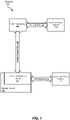
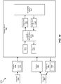
- FIG. 1 is a block diagram of an exemplary cache-coherent storage system 100.
- Cache-coherent storage system 100 may include one or more host processor(s) 102 (e.g., host central processing units (CPUs)) directly attached to a host-connected memory 104 via a memory bus 106 and a storage device 108 directly attached to a device-connected memory 110 via a memory bus 112.
- host processor(s) 102 and storage device 108 may be interconnected through a cache-coherent bus 116.
- host processor(s) 102 may read and write data directly to host-connected memory 104 through memory bus 106 and indirectly to device-connected memory 110 through cache-coherent bus 116.
- storage device 108 may read and write data directly to device-connected memory 110 through memory bus 112 and indirectly to host-connected memory 104 through cache-coherent bus 116.
- host processor(s) 102, storage system 108, and/or any number of additional devices, not shown may reference and/or access memory locations contained in host-connected memory 104 and device-connected memory 110 using a coherent memory space or address space (e.g., coherent memory space 710 illustrated in FIGS. 7-10 ) that includes one or more host address ranges mapped to cacheable memory locations contained in host-connected memory 104 and/or one or more address ranges mapped to cacheable memory locations contained in device-connected memory 110.
- coherent memory space or address space e.g., coherent memory space 710 illustrated in FIGS. 7-10
- storage device 108 may include an in-line transformation engine 114 for performing in-line transformations on data written to or read from device-connected memory 110 via cache-coherent bus 116.
- In-line transformation engine 114 may include any suitable physical processor or processors capable of performing in-line transformations (e.g., encryption operations, compression operations, transcription operations, etc.) on data. Examples of in-line transformation engine 114 include, without limitation, microprocessors, microcontrollers, Central Processing Units (CPUs), Digital signal processors (DSPs), Field-Programmable Gate Arrays (FPGAs), Application-Specific Integrated Circuits (ASICs), portions of one or more of the same, variations or combinations of one or more of the same, or any other suitable physical processor.
- CPUs Central Processing Units
- DSPs Digital signal processors
- FPGAs Field-Programmable Gate Arrays
- ASICs Application-Specific Integrated Circuits
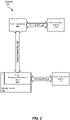
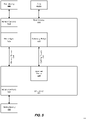
- in-line transformation engine 114 may include an in-line encryption/decryption engine 200 (e.g., as shown in FIG. 2 ) capable of performing in-line encryption/decryption operations on data written to or read from device-connected memory 110 via cache-coherent bus 116 and/or an in-line compression/decompression engine 300 (e.g., as shown in FIG. 3 ) capable of performing one or more in-line compression/decompression operations on data written to or read from device-connected memory 110 via cache-coherent bus 116.
- an in-line encryption/decryption engine 200 e.g., as shown in FIG. 2
- in-line compression/decompression engine 300 e.g., as shown in FIG. 3
- Host-connected memory 104 and/or device-connected memory 110 may represent any type of form of memory capable of storing cacheable data. Examples of host-connected memory 104 and/or device-connected memory 110 include, without limitation, dynamic randomly addressable memory (DRAM), static randomly addressable memory (SRAM), High Bandwidth Memory (HBM), cache memory, volatile memory, non-volatile memory (e.g., Flash memory), or any other suitable form of computer memory.
- Memory bus 106 and memory bus 112 may represent any internal memory bus suitable for interfacing with host-connected memory 104 and/or device-connected memory 110.
- Examples of memory bus 106 and memory bus 112 include, without limitation, Double Data Rate (DDR) buses, Serial ATA (SATA) buses, Serial Attached SCSI (SAS) buses, High Bandwidth Memory (HBM) buses, Peripheral Component Interconnect Express (PCIe) buses, and the like.
- DDR Double Data Rate
- SATA Serial ATA
- SAS Serial Attached SCSI
- HBM High Bandwidth Memory
- PCIe Peripheral Component Interconnect Express
- Cache-coherent bus 116 may represent any high-bandwidth and/or low-latency chip-to-chip interconnect, external bus, or expansion bus capable of hosting a providing connectivity (e.g., I/O, coherence, and/or memory semantics) between host processor(s) 102 and external devices or packages such as caching devices, workload accelerators (e.g., Graphics Processing Unit (GPU) devices, Field-Programmable Gate Array (FPGA) devices, Application-Specific Integrated Circuit (ASIC) devices, machine learning accelerators, tensor and vector processor units, etc.), memory expanders, and memory buffers.
- workload accelerators e.g., Graphics Processing Unit (GPU) devices, Field-Programmable Gate Array (FPGA) devices, Application-Specific Integrated Circuit (ASIC) devices, machine learning accelerators, tensor and vector processor units, etc.
- cache-coherent bus 116 may include a standardized interconnect (e.g., a Peripheral Component Interconnect Express (PCIe) bus), a proprietary interconnect, or some combination thereof.
- PCIe Peripheral Component Interconnect Express
- cache-coherent bus 116 may include a compute express link (CXL) interconnect such as those illustrated in FIGS. 4 and 5 .
- CXL compute express link
- Example system 100 in FIG. 1 may be implemented in a variety of ways. For example, all or a portion of example system 100 may represent portions of an example system 400 in FIG. 4 .
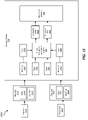
- system 400 may include a host processor 410 connected to a CXL device 420 via a compute express link 430.
- host processor 410 may be directly connected to a host memory440 via an internal memory bus
- CXL device 420 may be directly connected to a device memory 450 via an internal memory bus.
- the internal components of host processor 410 may communicate over compute express link 430 with the internal components of CXL device 420 using one or more CXL protocols (e.g., a memory protocol 432, a caching protocol 434, and/or an I/O protocol 436) that are multiplexed by multiplexing logic 412 and 422.
- CXL protocols e.g., a memory protocol 432, a caching protocol 434, and/or an I/O protocol 436
- host processor 410 may include one or more processing core(s) 416 that are capable of accessing and caching data stored to host memory 440 and device memory 450 via coherence/cache logic 414. Host processor 410 may also include an I/O device 419 that is capable of communication over compute express link 430 via PCIe logic 418. As shown in FIG. 5 , in some embodiments, host processor 410 may include a root complex 510 (e.g., a PCIe compatible root complex) that connects one or more of cores 416 to host memory 440 and device memory 450.
- a root complex 510 e.g., a PCIe compatible root complex
- root complex 510 may include a memory controller 512 for managing read and write operations to host memory 440, a home agent 514 for performing translations between physical, channel, and/or system memory addresses, and a coherency bridge 516 for resolving system wide coherency for a given host address.
- CXL device 420 may include device logic 424 for performing memory and CXL protocol tasks.
- device logic 424 may include one or more in-line transformation engines, such as those described in connection with FIGS. 1-3 , and a memory controller 522 that manages read and write operations to device memory 450 (e.g., as shown in FIG. 5 ).
- CXL device 420 may include a coherent cache 524 for caching host-managed data.
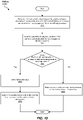
- FIG. 6 is a flow diagram of an exemplary computer-implemented method 600 for transforming data in-line with reads and writes to coherent host-managed device memory.
- the steps shown in FIG. 6 may be performed by any suitable computer-executable code and/or computing system, including the system(s) illustrated in FIGS. 1 , 2 , 3 , 4 , and 5 .
- each of the steps shown in FIG. 6 may represent an algorithm whose structure includes and/or is represented by multiple sub-steps, examples of which will be provided in greater detail below.
- one or more of the systems described herein may receive, from an external host processor, a request to access a host address of a shared coherent memory space.
- in-line transformation engine 114 may, as part of storage device 108, receive, from host processor 102 via cache-coherent interconnect 116, a request to access host address 712(M) of a shared coherent memory space 710 of host processor 102.
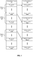
- FIG. 7 illustrates an exemplary coherent memory space 710 having host addresses 712(1)-(Z) that have been mapped to (1) physical memory locations of host physical memory 104 and (2) physical memory locations of device physical memory 110.
- a memory range 713 of coherent memory space 710 may be mapped to memory locations 719(1)-(N) of host physical memory 104
- a memory range 715 of coherent memory space 710 may be mapped to memory locations 722(1)-(N) of device physical memory 110
- a memory range 717 of coherent memory space 710 may be mapped to memory locations 722(Z-Y)-(Z) of device physical memory 110.
- host processors or accelerators that share access to coherent memory space 710 may read or write data to host physical memory 104 by accessing the host addresses in memory range 713.
- host processors or accelerators that share access to coherent memory space 710 may read or write data to device physical memory 110 by accessing the host addresses in either of memory ranges 715 or 717.
- one or more regions of the disclosed coherent memory spaces may be associated with one or more reversable in-line transformations or conversions (e.g., lossless or lossy data manipulations such as encryption operations, compression operations, transcription operations, etc.) that may be performed on any data written to those regions.
- memory range 715 of coherent memory space 710 may be designated for storing encrypted data and/or may be associated with a particular encryption algorithm such that the disclosed storage devices may automatically encrypt any data written to memory range 715 of coherent memory space 710 before storage to encrypted memory 800 of device physical memory 110.
- one or more regions of the disclosed coherent memory spaces may not be associated with any in-line transformation or conversion.
- memory range 717 of coherent memory space 710 may not be designated for storing encrypted data such that the disclosed storage devices may automatically store, as unencrypted data to unencrypted memory 802 of device physical memory 110, any data written to memory range 717 of coherent memory space 710.
- memory range 715 of coherent memory space 710 is shown as being designated for storing compressed data such that the disclosed storage devices may automatically compress any data written to memory range 715 of coherent memory space 710 before storage to compressed memory 900 of device physical memory 110.
- memory range 717 of coherent memory space 710 may be designated for storing uncompressed data such that any data written to memory range 717 of coherent memory space 710 may be stored uncompressed to uncompressed memory 902 of device physical memory 110.
- memory ranges of coherent memory space 710 may be associated with different encryption/compression algorithms.
- memory range 715 of coherent memory space 710 may be associated with a compression algorithm 1000 such that the disclosed storage devices may automatically compress any data written to memory range 715 of coherent memory space 710 using compression algorithm 1000 before storage to compressed memory 1002 of device physical memory 110.
- memory range 717 of coherent memory space 710 may be associated with a different compression algorithm 1004 such that the disclosed storage devices may automatically compress any data written to memory range 717 of coherent memory space 710 using compression algorithm 1004 before storage to compressed memory 1006 of device physical memory 110.
- one or more of the systems described herein may determine if any request received at step 610 is a write request or a read request. If the request is a request to write data, flow of method 600 may continue to step 630.
- one or more of the systems described herein may perform an in-line transformation on the data included in the write request received at step 610 to produce transformed data.
- in-line transformation engine 114 may, as part of storage device 108, perform an in-line transformation on data received from host processor 102 via cache-coherent bus 116.
- the systems described herein may determine what, if any, in-line transformations should be performed on the received data by determining if the host address falls within a range of addresses designated for an in-line transformation. If the host address falls within a range of host addresses designated for one or more in-line transformations, the systems described herein may perform the one or more in-line transformations on the received data. Additionally or alternatively, if the host address falls within more than one range of host addresses, each being separately designated for an in-line transformation, the systems described herein may perform each in-line transformation on the received data. However, if the host address does not fall within a range of host addresses designated for an in-line transformation, the systems described herein may refrain from performing any in-line transformations on the received data.
- one or more of the systems described herein may write the transformed data to the physical address of the device-attached physical memory mapped to the host address received at step 610.
- in-line transformation engine 114 may, as part of storage device 108, write data to memory location 722(1) in response to receiving a request to write the data to host address 712(M) of shared coherent memory space 710.
- Exemplary method 600 in FIG. 6 may terminate upon the completion of step 640.
- step 650 one or more of the systems described herein may read previously transformed data from the physical address of the device-attached physical memory mapped to the host address received at step 610.
- in-line transformation engine 114 may, as part of storage device 108, read data from memory location 722(1) in response to receiving a request to access host address 712(M) of shared coherent memory space 710.
- one or more of the systems described herein may perform a reversing in-line transformation on previously transformed data to reproduce original data.
- the systems described herein may determine what, if any, reversing in-line transformations need to be performed on the data by determining if the host address falls within a range of addresses designated for an in-line transformation. If the host address falls within a range of host addresses designated for one or more in-line transformations, the systems described herein may perform one or more corresponding reversing in-line transformations on the data to restore the data to its original form.
- the systems described herein may perform the corresponding reversing in-line transformations on the data. However, if the host address does not fall within a range of host addresses designated for an in-line transformation, the systems described herein may refrain from performing any reversing in-line transformations on the data.
- one or more of the systems described herein may return the original data to the external host processor via the cache-coherent interconnect.
- in-line transformation engine 114 may, as part of storage device 108, return original data to host processor 102 via cache-coherent interconnect 116.
- Exemplary method 600 in FIG. 6 may terminate upon the completion of step 670.
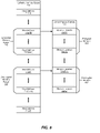
- FIG. 11 is a flow diagram of an exemplary computer-implemented method 1100 for encrypting data in-line with writes to coherent host-managed device memory.
- the steps shown in FIG. 11 may be performed by any suitable computer-executable code and/or computing system, including the system(s) illustrated in FIGS. 1 , 2 , 3 , 4 , and 5 .
- each of the steps shown in FIG. 11 may represent an algorithm whose structure includes and/or is represented by multiple sub-steps, examples of which will be provided in greater detail below.
- one or more of the systems described herein may receive, from an external host processor, a request to write data to a host address of a shared coherent memory space.
- in-line encryption/decryption engine 200 may receive a request 1312 from a requester 1310 (e.g., a host processor, core, or thread) to write data 1314 to host address 712(M) mapped to encrypted memory 800 and/or may receive a request 1332 from a requester 1330 to write data 1334 to host address 712 (M+N) also mapped to encrypted memory 800.
- a requester 1610 e.g., a host processor, core, or thread
- M+N host address 712
- in-line encryption/decryption engine 200 may receive a request 1612 from a requester 1610 to write data 1614 to host address 712(X) mapped to unencrypted memory 802.
- one or more of the systems described herein may determine whether a host address received in a request to write data falls within a range designated as encrypted memory. If a host address does fall within a range designated as encrypted memory, flow of method 1100 may continue to step 1130. For example, in-line encryption/decryption engine 200 may proceed to step 1130 after determining that host addresses 712(M) and 712(M+N) contained in requests 1312 and 1332 are mapped in coherent memory space 710 to encrypted memory range 715.
- one or more of the systems described herein may encrypt the data received at step 1110.
- in-line encryption/decryption engine 200 may generate encrypted data 1320 and encrypted data 1340 by respectively encrypting data 1314 using a cryptographic key 1318 and data 1334 using a cryptographic key 1338.
- the systems described herein may encrypt data using any suitable cryptographic function, algorithm, or scheme.
- the disclosed systems and methods may manage cryptographic keys at a processor, core, or thread level such that one processor, core, or thread cannot access the encrypted data of another processor, core, or thread.
- the disclosed systems may decrease the attack surface of shared system memory and/or prevent data stored to shared system memory from being access by unauthorized processors, cores, or threads or malicious intruders that have gained access to a processor, core, or thread with the ability to access the shared system memory.
- FIG. 12 is a flow diagram of an exemplary computer-implemented method 1200 for identifying cryptographic keys for performing encryption/decryption operations.
- a requester identifier e.g., a host identifier, a core identifier, or a thread identifier
- in-line encryption/decryption engine 200 may extract an identifier 1316 of requester 1310 from request 1312 and an identifier 1336 of requester 1330 from request 1332.
- in-line encryption/decryption engine 200 may extract identifier 1316 of requester 1310 from request 1510 and identifier 1336 of requester 1330 from request 1514.
- the systems described herein may extract typical protocol identifiers for use in identifying cryptographic keys. Additionally or alternatively, the systems described herein may extract identifiers specifically provided by requesters for encryption purposes. In at least one embodiment, the requester identifiers may include a cryptographic key provided by a requester.
- one or more of the systems described herein may identify a cryptographic key by querying a key store for a cryptographic key associated with an extracted requester identifier.
- in-line encryption/decryption engine 200 may identify key 1318 and key 1338 by querying a key store for a cryptographic key associated with identifier 1316 and identifier 1336, respectively.
- one or more of the systems described herein may write the data encrypted at step 1130 to the physical address of the device-attached physical memory mapped to the host address received at step 1110.
- in-line encryption/decryption engine 200 may write encrypted data 1320 to memory location 722(1) and encrypted data 1340 to memory location 722(N) as shown in FIG. 13 .
- Exemplary method 1100 in FIG. 11 may terminate upon the completion of step 1140.
- step 1110 If the host address received at step 1110 did not fall within a range designated as encrypted memory, flow of method 1100 may continue from step 1120 to step 1150.
- in-line encryption/decryption engine 200 may proceed to step 1150 after determining that host address 712(X) contained in request 1612 has been mapped in coherent memory space 710 to unencrypted memory range 717.
- one or more of the systems described herein may write unencrypted data to a physical address of the device-attached physical memory mapped to the host address referenced in the request received at step 1110.
- in-line encryption/decryption engine 200 may write data 1614 to memory location 722(Z-Y) in unencrypted memory 802.
- Exemplary method 1100 in FIG. 11 may terminate upon the completion of step 1150.
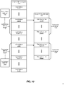
- FIG. 14 is a flow diagram of an exemplary computer-implemented method 1400 for decrypting data in-line with reads from coherent host-managed device memory.
- the steps shown in FIG. 14 may be performed by any suitable computer-executable code and/or computing system, including the system(s) illustrated in FIGS. 1 , 2 , 3 , 4 , and 5 .
- each of the steps shown in FIG. 14 may represent an algorithm whose structure includes and/or is represented by multiple sub-steps, examples of which will be provided in greater detail below.
- one or more of the systems described herein may receive, from an external host processor, a request to read data from a host address of a shared coherent memory space.
- in-line encryption/decryption engine 200 may receive a request 1510 from requester 1310 to read data 1314 from host address 712(M) mapped to encrypted memory 800 and/or may receive a request 1514 from requester 1330 to read data 1334 from host address 712(M+N) mapped to encrypted memory 800.
- FIG. 16 as another example, in-line encryption/decryption engine 200 may receive a request 1622 from a requester 1620 to read data 1614 from host address 712(X) mapped to unencrypted memory 802.
- one or more of the systems described herein may read previously stored data from the physical address of the device-attached physical memory that is mapped to the host address received at step 1410.
- in-line encryption/decryption engine 200 may read encrypted data 1320 from memory location 722(1) in response to receiving request 1510 to read data from host address 712(M) of shared coherent memory space 710.
- in-line encryption/decryption engine 200 may read encrypted data 1340 from memory location 722(N) in response to receiving request 1514 to read data from host address 712(M+N) of shared coherent memory space 710.
- in-line encryption/decryption engine 200 may read unencrypted data 1614 from memory location 722(Z-Y) in response to receiving request 1622 to read data from host address 712(X) of shared coherent memory space 710.
- one or more of the systems described herein may determine whether a host address received in a request to read data falls within a range designated as encrypted memory. If a host address does fall within a range designated as encrypted memory, flow of method 1400 may continue to step 1440. For example, in-line encryption/decryption engine 200 may proceed to step 1440 after determining that host addresses 712(M) and 712(M+N) contained in requests 1510 and 1514 are mapped in coherent memory space 710 to encrypted memory range 715.
- one or more of the systems described herein may decrypt the encrypted data read from device memory at step 1420.
- in-line encryption/decryption engine 200 may regenerate data 1314 and data 1334 by respectively decrypting data 1320 using cryptographic key 1318 and encrypted data 1340 using cryptographic key 1338.
- the systems described herein may decrypt data using any suitable cryptographic function, algorithm, or scheme.
- one or more of the systems described herein may return the original data to the external host processor via the cache-coherent interconnect at step 1450. For example, as shown in exemplary data flow 1500 in FIG.
- in-line encryption/decryption engine 200 may return data 1314 to requester 1310 in a response 1512 and data 1334 to requester 1330 in a response 1516.
- Exemplary method 1400 in FIG. 14 may terminate upon the completion of step 1450.
- step 1410 If the host address received at step 1410 did not fall within a range designated as encrypted memory, flow of method 1400 may continue from step 1430 to step 1460.
- in-line encryption/decryption engine 200 may proceed to step 1460 after determining that host address 712(X) contained in request 1612 has been mapped in coherent memory space 710 to unencrypted memory range 717.
- step 1460 one or more of the systems described herein may return data read from device memory to the external host processor via the cache-coherent interconnect without decrypting the data. For example, as shown in FIG.
- in-line encryption/decryption engine 200 may return data 1614 read from unencrypted memory 802 to requester 1620 in a response 1624 without performing a decryption operation on data 1614.
- Exemplary method 1400 in FIG. 14 may terminate upon the completion of step 1460.
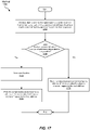
- FIG. 17 is a flow diagram of an exemplary computer-implemented method 1700 for compressing data in-line with writes to coherent host-managed device memory.
- the steps shown in FIG. 17 may be performed by any suitable computer-executable code and/or computing system, including the system(s) illustrated in FIGS. 1 , 2 , 3 , 4 , and 5 .
- each of the steps shown in FIG. 17 may represent an algorithm whose structure includes and/or is represented by multiple sub-steps, examples of which will be provided in greater detail below.
- one or more of the systems described herein may receive, from an external host processor, a request to write data to a host address of a shared coherent memory space.
- in-line compression/decompression engine 300 may receive a request 1812 from a requester 1810 (e.g., a host processor, core, or thread) to write data 1814 to host address 712(M) mapped to compressed memory 900.
- requester 1810 e.g., a host processor, core, or thread
- in-line compression/decompression engine 300 may receive a request 2012 from a requester 2010 to write data 2014 to host address 712(X) mapped to uncompressed memory 902.
- one or more of the systems described herein may determine whether a host address received in a request to write data falls within a range designated as compressed memory. If a host address does fall within a range designated as compressed memory, flow of method 1700 may continue to step 1730. For example, in-line compression/decompression engine 300 may proceed to step 1730 after determining that host address 712(M) contained in request 1812 is mapped in coherent memory space 710 to compressed memory range 715.
- one or more of the systems described herein may compress the data received at step 1710.
- in-line compression/decompression engine 300 may generate compressed data 1816 by compressing data 1814.
- the systems described herein may compress data using any suitable compression function, algorithm, or scheme.
- one or more of the systems described herein may write the data compressed at step 1730 to the physical address of the device-attached physical memory mapped to the host address received at step 1710.
- in-line compression/decompression engine 300 may write compressed data 1816 to memory location 722(1) as shown in FIG. 18 .
- Exemplary method 1700 in FIG. 17 may terminate upon the completion of step 1740.
- step 1750 If the host address received at step 1710 did not fall within a range designated as compressed memory, flow of method 1700 may continue from step 1720 to step 1750.
- in-line compression/decompression engine 300 may proceed to step 1750 after determining that host address 712(X) contained in request 2012 has been mapped in coherent memory space 710 to uncompressed memory range 717.
- one or more of the systems described herein may write uncompressed data to a physical address of the device-attached physical memory mapped to the host address referenced in the request received at step 1710.
- in-line compression/decompression engine 300 may write data 2014 to memory location 722(Z-Y) in uncompressed memory 902.
- Exemplary method 1700 in FIG. 17 may terminate upon the completion of step 1750.
- FIG. 19 is a flow diagram of an exemplary computer-implemented method 1900 for decompressing data in-line with reads from coherent host-managed device memory.
- the steps shown in FIG. 19 may be performed by any suitable computer-executable code and/or computing system, including the system(s) illustrated in FIGS. 1 , 2 , 3 , 4 , and 5 .
- each of the steps shown in FIG. 19 may represent an algorithm whose structure includes and/or is represented by multiple sub-steps, examples of which will be provided in greater detail below.
- one or more of the systems described herein may receive, from an external host processor, a request to read data from a host address of a shared coherent memory space.
- in-line compression/decompression engine 300 may receive a request 1822 from a requester 1820 to read data 1814 from host address 712(M) mapped to compressed memory 900.
- in-line compression/decompression engine 300 may receive a request 2022 from a requester 2020 to read data 2014 from host address 712(X) mapped to uncompressed memory 902.
- one or more of the systems described herein may read previously stored data from the physical address of the device-attached physical memory that is mapped to the host address received at step 1910.
- in-line compression/decompression engine 300 may read compressed data 1816 from memory location 722(1) in response to receiving request 1822 to read data from host address 712(M) of shared coherent memory space 710.
- in-line compression/decompression engine 300 may read data 2014 from memory location 722(Z-Y) in response to receiving request 2022 to read data from host address 712(X) of shared coherent memory space 710.
- one or more of the systems described herein may determine whether a host address received in a request to read data falls within a range designated as compressed memory. If a host address does fall within a range designated as compressed memory, flow of method 1900 may continue to step 1940. For example, in-line compression/decompression engine 300 may proceed to step 1940 after determining that host address 712 (M) contained in requests 1822 is mapped in coherent memory space 710 to compressed memory range 715.
- M host address 712
- one or more of the systems described herein may decompress the compressed data read from device memory at step 1920.
- in-line compression/decompression engine 300 may regenerate data 1814 by decompressing compressed data 1816.
- the systems described herein may decompress data using any suitable decompression function, algorithm, or scheme.
- one or more of the systems described herein may return the original data to the external host processor via the cache-coherent interconnect at step 1950.
- in-line compression/decompression engine 300 may return data 1814 to requester 1820 in a response 1824.
- Exemplary method 1900 in FIG. 19 may terminate upon the completion of step 1950.
- step 1900 may continue from step 1930 to step 1960.
- in-line compression/decompression engine 300 may proceed to step 1960 after determining that host address 712(X) contained in request 2022 has been mapped in coherent memory space 710 to uncompressed memory range 717.
- one or more of the systems described herein may return data read from device memory to the external host processor via the cache-coherent interconnect without decompressing the data.
- in-line compression/decompression engine 300 may return data 2014 read from uncompressed memory 902 to requester 2020 in a response 2024 without performing a decompression operation on data 2014.
- Exemplary method 1900 in FIG. 19 may terminate upon the completion of step 1960.
- embodiments of the present disclosure may perform various in-line encryption/decryption and/or compression/decompression operations when reading and/or writing data to shared device-attached memory resources.
- the disclosed devices may perform these in-line transformations in a way that is transparent to external host processors and/or accelerators.
- the disclose devices may enable a coherent memory space to be partitioned into multiple regions, each region being associated with one or more in-line transformations, such that external host processors and/or accelerators are able to choose an appropriate in-line transformation by writing data to an associated region of memory.
- a coherent memory space may include one or more encrypted sections, one or more unencrypted sections, one or more compressed sections, and/or one or more uncompressed sections.
- the disclosed systems and methods may manage cryptographic keys at a processor, core, or thread level such that one processor, core, or thread cannot access the encrypted data of another processor, core, or thread.
- the disclosed systems may decrease the attack surface of shared system memory and/or prevent data stored to shared system memory from being access by unauthorized entities or malicious intruders.
- the disclosed systems may use multiple compression algorithms, each being associated with one or more memory regions and/or types of stored data.
- a storage device may include (1) a device-attached physical memory accessible to an external host processor via a cache-coherent interconnect, addresses of the device-attached physical memory being mapped to a coherent memory space of the external host processor, and (2) one or more internal physical processors adapted to (a) receive, from the external host processor via the cache-coherent interconnect, a request to write first data to a host address of the coherent memory space of the external host processor, (b) perform an in-line transformation on the first data to generate second data, and (c) write the second data to a physical address of the device-attached physical memory corresponding to the host address.
- Example 2 The storage device of Example 1, wherein the in-line transformation may include an encryption operation, and the one or more internal physical processors may be adapted to (1) perform the in-line transformation by performing the encryption operation on the first data and (2) write the second data by writing the encrypted first data to the physical address of the device-attached physical memory.
- the in-line transformation may include an encryption operation
- the one or more internal physical processors may be adapted to (1) perform the in-line transformation by performing the encryption operation on the first data and (2) write the second data by writing the encrypted first data to the physical address of the device-attached physical memory.
- Example 3 The storage device of any of Examples 1-2, further including a cryptographic-key store containing multiple cryptographic keys, each of the cryptographic keys being mapped to one or more requester identifiers.
- the request may include a requester identifier previously mapped to a cryptographic key in the cryptographic-key store, and the one or more internal physical processors may be adapted to (1) use the requester identifier to locate the cryptographic key and (2) use the cryptographic key to perform the encryption operation on the first data.
- Example 4 The storage device of any of Examples 1-3, wherein the requester identifier may include an identifier of a thread executing on the external host processor, the thread having generated the request.
- Example 5 The storage device of any of Examples 1-4, wherein the one or more internal physical processors may be further adapted to receive, from the external host processor, a second request to write third data to a second host address of the coherent memory space of the external host processor.
- the second request may include a second requester identifier previously mapped to a second cryptographic key in the cryptographic-key store
- the second requester identifier may include a second identifier of a second thread executing on the external host processor
- the second thread may have generated the second request.
- the one or more internal physical processors may also be further adapted to (1) translate the second host address into a second device address of the device-attached physical memory, (2) use the second requester identifier to locate the second cryptographic key, (3) use the second cryptographic key to perform the encryption operation on the third data, and (4) write the encrypted third data to the second physical address of the device-attached physical memory.
- Example 6 The storage device of any of Examples 1-5, wherein (1) a first range of addresses of the coherent memory space of the external host processor may be designated as encrypted memory, the host address falling within the first range of addresses, (2) a second range of addresses of the coherent memory space of the external host processor may be designated as unencrypted memory, and (3) the one or more internal physical processors may be adapted to perform the encryption operation on the first data in response to determining that the host address falls within the first range of addresses.
- Example 7 The storage device of any of Examples 1-6, wherein the one or more internal physical processors may be further adapted to (1) receive, from the external host processor, a second request to write third data to a second host address of the coherent memory space of the external host processor, the second host address falling within the second range of addresses, (2) translate the second host address into a second device address of the device-attached physical memory, (3) refrain from encrypting the second data in response to determining that the second host address falls within the second range of addresses, and (4) write the unencrypted third data to the second physical address of the device-attached physical memory.
- Example 8 The storage device of any of Examples 1-7, wherein the in-line transformation may include a compression operation, and the one or more internal physical processors may be adapted to (1) perform the in-line transformation by performing the compression operation on the first data and (2) write the second data by writing the compressed first data to the physical address of the device-attached physical memory.
- the in-line transformation may include a compression operation
- the one or more internal physical processors may be adapted to (1) perform the in-line transformation by performing the compression operation on the first data and (2) write the second data by writing the compressed first data to the physical address of the device-attached physical memory.
- Example 9 The storage device of any of Examples 1-8, wherein (1) a first range of addresses of the coherent memory space of the external host processor may be designated for storing a first type of data associated with the compression operation, the host address falling within the first range of addresses, (2) a second range of addresses of the coherent memory space of the external host processor may be designated for storing a second type of data associated with a second compression operation, and (3) the one or more internal physical processors may be adapted to perform the compression operation on the first data in response to determining that the host address falls within the first range of addresses.
- Example 10 The storage device of any of Examples 1-9, wherein the one or more internal physical processors may be further adapted to (1) receive, from the external host processor, a second request to write third data to a second host address of the coherent memory space of the external host processor, the second host address falling within the second range of addresses, (2) translate the second host address into a second device address of the device-attached physical memory, (3) perform the second compression operation, instead of the compression operation, on the third data in response to determining that the second host address falls within the second range of addresses, and (4) write the compressed third data to the second physical address of the device-attached physical memory.
- Example 11 A storage device including (1) a device-attached physical memory managed by and accessible to an external host processor via a cache-coherent interconnect, wherein addresses of the device-attached physical memory may be mapped to a coherent memory space of the external host processor, and (2) one or more internal physical processors adapted to (a) receive, from the external host processor via the cache-coherent interconnect, a request to read from a host address of the coherent memory space of the external host processor, (b) translate the host address into a device address of the device-attached physical memory, (c) read first data from the physical address of the device-attached physical memory, (d) perform an in-line transformation on the first data to generate second data, and (e) return the second data to the external host processor via the cache-coherent interconnect.
- Example 12 The storage device of Example 11, wherein the in-line transformation may include a decryption operation, and the one or more internal physical processors may be adapted to (1) perform the in-line transformation by performing the decryption operation on the first data and (2) return the second data by returning the decrypted first data to the external host processor via the cache-coherent interconnect.
- the in-line transformation may include a decryption operation
- the one or more internal physical processors may be adapted to (1) perform the in-line transformation by performing the decryption operation on the first data and (2) return the second data by returning the decrypted first data to the external host processor via the cache-coherent interconnect.
- Example 13 The storage device of any of Examples 1-12, further including a cryptographic-key store containing multiple cryptographic keys, each of the cryptographic keys being mapped to one or more requester identifiers.
- the request may include a requester identifier previously mapped to a cryptographic key in the cryptographic-key store, and the one or more internal physical processors may be adapted to use the requester identifier to locate the cryptographic key and use the cryptographic key to perform the decryption operation on the first data.
- Example 14 The storage device of any of Examples 1-13, wherein the requester identifier may include an identifier of a thread executing on the external host processor, the thread having generated the request.
- Example 15 The storage device of any of Examples 1-14, wherein the one or more internal physical processors may be further adapted to receive, from the external host processor, a second request to read from a second host address of the coherent memory space of the external host processor.
- the second request may include a second requester identifier previously mapped to a second cryptographic key in the cryptographic-key store
- the second requester identifier may include a second identifier of a second thread executing on the external host processor
- the second thread may have generated the second request.
- the one or more internal physical processors may be further adapted to (1) translate the second host address into a second device address of the device-attached physical memory, (2) use the second requester identifier to locate the second cryptographic key, (3) use the second cryptographic key to perform the decryption operation on the third data, and (4) return the decrypted third data to the external host processor via the cache-coherent interconnect.
- Example 16 The storage device of any of Examples 1-15, wherein a first range of addresses of the coherent memory space of the external host processor may be designated as encrypted memory, the host address falling within the first range of addresses, a second range of addresses of the coherent memory space of the external host processor may be designated as unencrypted memory, and the one or more internal physical processors may be adapted to perform the decryption operation on the first data in response to determining that the host address falls within the first range of addresses.
- Example 17 The storage device of any of Examples 1-16, wherein the one or more internal physical processors may be further adapted to (1) receive, from the external host processor, a request to read from a second host address of the coherent memory space of the external host processor, the second host address falling within the second range of addresses, (2) translate the second host address into a second device address of the device-attached physical memory, (3) refrain from decrypting the second data in response to determining that the second host address falls within the second range of addresses, and (4) return the third data to the external host processor via the cache-coherent interconnect.
- Example 18 The storage device of any of Examples 1-17, wherein the in-line transformation may include a decompression operation, the one or more internal physical processors may be adapted to (1) perform the in-line transformation by performing the decompression operation on the first data and (2) return the second data by returning the decompressed first data to the external host processor via the cache-coherent interconnect.
- the in-line transformation may include a decompression operation
- the one or more internal physical processors may be adapted to (1) perform the in-line transformation by performing the decompression operation on the first data and (2) return the second data by returning the decompressed first data to the external host processor via the cache-coherent interconnect.
- Example 19 The storage device of any of Examples 1-18, wherein a first range of addresses of the coherent memory space of the external host processor may be designated for storing a first type of data associated with the decompression operation, the host address falling within the first range of addresses, a second range of addresses of the coherent memory space of the external host processor may be designated for storing a second type of data associated with a second decompression operation, and the one or more internal physical processors may be adapted to perform the decompression operation on the first data in response to determining that the host address falls within the first range of addresses.
- a computer-implemented method may include (1) receiving, from an external host processor via a cache-coherent interconnect, a request to access a host address of a coherent memory space of the external host processor, wherein physical addresses of a device-attached physical memory may be mapped to the coherent memory space of the external host processor, (2) when the request is to write data to the host address, (a) performing an in-line transformation on the data to generate second data and (b) writing the second data to the physical address of the device-attached physical memory mapped to the host address, and (3) when the request is to read data from the host address, (a) reading the data from the physical address of the device-attached physical memory mapped to the host address, (b) performing a reversing in-line transformation on the data to generate second data, and (c) returning the second data to the external host processor via the cache-coherent interconnect.
- computing devices and systems described and/or illustrated herein broadly represent any type or form of computing device or system capable of executing computer-readable instructions, such as those contained within the modules described herein.
- these computing device(s) may each include at least one memory device and at least one physical processor.
- the term "memory device” generally refers to any type or form of volatile or non-volatile storage device or medium capable of storing data and/or computer-readable instructions.
- a memory device may store, load, and/or maintain one or more of the modules described herein.
- Examples of memory devices include, without limitation, Random Access Memory (RAM), Read Only Memory (ROM), flash memory, Hard Disk Drives (HDDs), Solid-State Drives (SSDs), optical disk drives, caches, variations or combinations of one or more of the same, or any other suitable storage memory.
- the term "physical processor” generally refers to any type or form of hardware-implemented processing unit capable of interpreting and/or executing computer-readable instructions.
- a physical processor may access and/or modify one or more modules stored in the above-described memory device.
- Examples of physical processors include, without limitation, microprocessors, microcontrollers, Central Processing Units (CPUs), Field-Programmable Gate Arrays (FPGAs) that implement softcore processors, Application-Specific Integrated Circuits (ASICs), portions of one or more of the same, variations or combinations of one or more of the same, or any other suitable physical processor.
- modules described and/or illustrated herein may represent portions of a single module or application.
- one or more of these modules may represent one or more software applications or programs that, when executed by a computing device, may cause the computing device to perform one or more tasks.
- one or more of the modules described and/or illustrated herein may represent modules stored and configured to run on one or more of the computing devices or systems described and/or illustrated herein.
- One or more of these modules may also represent all or portions of one or more special-purpose computers configured to perform one or more tasks.
- one or more of the modules described herein may transform data, physical devices, and/or representations of physical devices from one form to another.
- one or more of the modules recited herein may receive data to be transformed over a cache-coherent interconnect, transform the data (e.g., by encryption or compression), output a result of the transformation to device-connected memory, and use the result of the transformation to respond to future read requests for the data after reversing any transformations previously made.
- one or more of the modules recited herein may transform a processor, volatile memory, non-volatile memory, and/or any other portion of a physical computing device from one form to another by executing on the computing device, storing data on the computing device, and/or otherwise interacting with the computing device.
- the term "computer-readable medium” generally refers to any form of a device, carrier, or medium capable of storing or carrying computer-readable instructions.
- Examples of computer-readable media include, without limitation, transmission-type media, such as carrier waves, and non-transitory-type media, such as magnetic-storage media (e.g., hard disk drives, tape drives, and floppy disks), optical-storage media (e.g., Compact Disks (CDs), Digital Video Disks (DVDs), and BLU-RAY disks), electronic-storage media (e.g., solid-state drives and flash media), and other distribution systems.
- transmission-type media such as carrier waves
- non-transitory-type media such as magnetic-storage media (e.g., hard disk drives, tape drives, and floppy disks), optical-storage media (e.g., Compact Disks (CDs), Digital Video Disks (DVDs), and BLU-RAY disks), electronic-storage media (e.g., solid-
Landscapes
- Engineering & Computer Science (AREA)
- Theoretical Computer Science (AREA)
- Physics & Mathematics (AREA)
- General Engineering & Computer Science (AREA)
- General Physics & Mathematics (AREA)
- Computer Security & Cryptography (AREA)
- Human Computer Interaction (AREA)
- Computer Hardware Design (AREA)
- Software Systems (AREA)
- Storage Device Security (AREA)
Applications Claiming Priority (1)
| Application Number | Priority Date | Filing Date | Title |
|---|---|---|---|
| US17/227,421 US20220327052A1 (en) | 2021-04-12 | 2021-04-12 | Systems and methods for transforming data in-line with reads and writes to coherent host-managed device memory |
Publications (1)
| Publication Number | Publication Date |
|---|---|
| EP4075285A1 true EP4075285A1 (de) | 2022-10-19 |
Family
ID=81307405
Family Applications (1)
| Application Number | Title | Priority Date | Filing Date |
|---|---|---|---|
| EP22167910.3A Withdrawn EP4075285A1 (de) | 2021-04-12 | 2022-04-12 | Systeme und verfahren zur transformation von daten inline mit lese- und schreibvorgängen in einen speicher mit kohärentem host-verwalteten vorrichtungsspeicher |
Country Status (3)
| Country | Link |
|---|---|
| US (1) | US20220327052A1 (de) |
| EP (1) | EP4075285A1 (de) |
| CN (1) | CN115203756A (de) |
Families Citing this family (3)
| Publication number | Priority date | Publication date | Assignee | Title |
|---|---|---|---|---|
| US12137161B2 (en) * | 2021-12-10 | 2024-11-05 | Amazon Technologies, Inc. | Limiting use of encryption keys in an integrated circuit device |
| US12387011B2 (en) * | 2022-10-24 | 2025-08-12 | Synopsys, Inc. | Secured computer memory |
| CN118779280B (zh) * | 2024-07-10 | 2025-02-25 | 北京超弦存储器研究院 | 降低总线负载的方法、cxl模组、处理系统和处理器芯片 |
Citations (6)
| Publication number | Priority date | Publication date | Assignee | Title |
|---|---|---|---|---|
| WO2017127084A1 (en) * | 2016-01-21 | 2017-07-27 | Hewlett-Packard Development Company, L.P. | Data cryptography engine |
| US20170371792A1 (en) * | 2016-06-24 | 2017-12-28 | Qualcomm Incorporated | Priority-based storage and access of compressed memory lines in memory in a processor-based system |
| US20180336158A1 (en) * | 2017-05-16 | 2018-11-22 | Dell Products L.P. | Systems and methods for data transfer with coherent and non-coherent bus topologies and attached external memory |
| US20190007202A1 (en) * | 2017-07-03 | 2019-01-03 | Stmicroelectronics Application Gmbh | Hardware Secure Module, Related Processing System, Integrated Circuit, Device and Method |
| US20190042402A1 (en) * | 2018-03-29 | 2019-02-07 | Intel Corporation | System, apparatus and method for providing key identifier information in a non-canonical address space |
| US20190095350A1 (en) * | 2017-09-25 | 2019-03-28 | David M. Durham | System, Apparatus And Method For Page Granular,Software Controlled Multiple Key Memory Encryption |
Family Cites Families (8)
| Publication number | Priority date | Publication date | Assignee | Title |
|---|---|---|---|---|
| US7190284B1 (en) * | 1994-11-16 | 2007-03-13 | Dye Thomas A | Selective lossless, lossy, or no compression of data based on address range, data type, and/or requesting agent |
| US20120144146A1 (en) * | 2010-12-03 | 2012-06-07 | International Business Machines Corporation | Memory management using both full hardware compression and hardware-assisted software compression |
| US10536441B2 (en) * | 2016-08-23 | 2020-01-14 | Texas Instruments Incorporated | Thread ownership of keys for hardware-accelerated cryptography |
| US11030117B2 (en) * | 2017-07-14 | 2021-06-08 | Advanced Micro Devices, Inc. | Protecting host memory from access by untrusted accelerators |
| US20210064549A1 (en) * | 2019-09-03 | 2021-03-04 | ScaleFlux, Inc. | Enhancing the speed performance and endurance of solid-state data storage devices with embedded in-line encryption engines |
| US11281579B2 (en) * | 2020-01-28 | 2022-03-22 | Intel Corporation | Cryptographic separation of MMIO on device |
| US12086424B2 (en) * | 2020-08-24 | 2024-09-10 | Intel Corporation | Memory encryption engine interface in compute express link (CXL) attached memory controllers |
| US11755500B2 (en) * | 2020-12-26 | 2023-09-12 | Intel Corporation | Cryptographic computing with disaggregated memory |
-
2021
- 2021-04-12 US US17/227,421 patent/US20220327052A1/en not_active Abandoned
-
2022
- 2022-04-12 EP EP22167910.3A patent/EP4075285A1/de not_active Withdrawn
- 2022-04-12 CN CN202210383017.4A patent/CN115203756A/zh active Pending
Patent Citations (6)
| Publication number | Priority date | Publication date | Assignee | Title |
|---|---|---|---|---|
| WO2017127084A1 (en) * | 2016-01-21 | 2017-07-27 | Hewlett-Packard Development Company, L.P. | Data cryptography engine |
| US20170371792A1 (en) * | 2016-06-24 | 2017-12-28 | Qualcomm Incorporated | Priority-based storage and access of compressed memory lines in memory in a processor-based system |
| US20180336158A1 (en) * | 2017-05-16 | 2018-11-22 | Dell Products L.P. | Systems and methods for data transfer with coherent and non-coherent bus topologies and attached external memory |
| US20190007202A1 (en) * | 2017-07-03 | 2019-01-03 | Stmicroelectronics Application Gmbh | Hardware Secure Module, Related Processing System, Integrated Circuit, Device and Method |
| US20190095350A1 (en) * | 2017-09-25 | 2019-03-28 | David M. Durham | System, Apparatus And Method For Page Granular,Software Controlled Multiple Key Memory Encryption |
| US20190042402A1 (en) * | 2018-03-29 | 2019-02-07 | Intel Corporation | System, apparatus and method for providing key identifier information in a non-canonical address space |
Also Published As
| Publication number | Publication date |
|---|---|
| CN115203756A (zh) | 2022-10-18 |
| US20220327052A1 (en) | 2022-10-13 |
Similar Documents
| Publication | Publication Date | Title |
|---|---|---|
| EP4075285A1 (de) | Systeme und verfahren zur transformation von daten inline mit lese- und schreibvorgängen in einen speicher mit kohärentem host-verwalteten vorrichtungsspeicher | |
| JP6292594B2 (ja) | 重複排除に基づくデータセキュリティ | |
| TWI594121B (zh) | 使用資料壓縮的快取技術 | |
| US20130227301A1 (en) | Using storage controller bus interfaces to secure data transfer between storage devices and hosts | |
| US11669455B2 (en) | Systems and methods for profiling host-managed device memory | |
| US12189948B2 (en) | Device and method to minimize off-chip access between host and peripherals | |
| CN111949372A (zh) | 一种虚拟机迁移方法、通用处理器及电子设备 | |
| US20190384638A1 (en) | Method, device and computer program product for data processing | |
| WO2022226029A1 (en) | Systems and methods for pre-processing and post-processing coherent host-managed device memory | |
| CN117744118A (zh) | 一种基于fpga的高速加密存储装置和方法 | |
| US10936212B2 (en) | Memory controller, method for performing access control to memory module | |
| WO2022236037A1 (en) | Systems and methods for enabling accelerator-based secure execution zones | |
| KR20240025455A (ko) | 해시 스토리지에서 캐싱을 수행하기 위한 시스템 및 방법 | |
| CN110007849A (zh) | 存储器控制器以及用于对存储模块进行访问控制的方法 | |
| US9218296B2 (en) | Low-latency, low-overhead hybrid encryption scheme | |
| WO2019041272A1 (zh) | 一种计算机内存数据加解密的方法及装置 | |
| JP7431791B2 (ja) | ストレージシステム及びデータ処理方法 | |
| TWI781464B (zh) | 用於資料之加密及解密的運算裝置 | |
| US20170322891A1 (en) | Device and method for secure data storage | |
| US20250173467A1 (en) | Systems, methods, and apparatus for memory device with data security protection | |
| US12547547B2 (en) | Multi-address space collectives engine | |
| US20260081773A1 (en) | Selective Encryption for Processing-in-Memory | |
| US20240241837A1 (en) | Data encryption and decryption system and data encryption and decryption method | |
| US20250307448A1 (en) | Storage Device with Hybrid Encryption Levels | |
| KR20240033958A (ko) | 메모리 시스템, 메모리 컨트롤러 및 그 동작 방법 |
Legal Events
| Date | Code | Title | Description |
|---|---|---|---|
| PUAI | Public reference made under article 153(3) epc to a published international application that has entered the european phase |
Free format text: ORIGINAL CODE: 0009012 |
|
| STAA | Information on the status of an ep patent application or granted ep patent |
Free format text: STATUS: THE APPLICATION HAS BEEN PUBLISHED |
|
| AK | Designated contracting states |
Kind code of ref document: A1 Designated state(s): AL AT BE BG CH CY CZ DE DK EE ES FI FR GB GR HR HU IE IS IT LI LT LU LV MC MK MT NL NO PL PT RO RS SE SI SK SM TR |
|
| STAA | Information on the status of an ep patent application or granted ep patent |
Free format text: STATUS: REQUEST FOR EXAMINATION WAS MADE |
|
| 17P | Request for examination filed |
Effective date: 20230105 |
|
| RBV | Designated contracting states (corrected) |
Designated state(s): AL AT BE BG CH CY CZ DE DK EE ES FI FR GB GR HR HU IE IS IT LI LT LU LV MC MK MT NL NO PL PT RO RS SE SI SK SM TR |
|
| STAA | Information on the status of an ep patent application or granted ep patent |
Free format text: STATUS: THE APPLICATION IS DEEMED TO BE WITHDRAWN |
|
| 18D | Application deemed to be withdrawn |
Effective date: 20241101 |