EP4072019A1 - A chip with pad tracking - Google Patents
A chip with pad tracking Download PDFInfo
- Publication number
- EP4072019A1 EP4072019A1 EP22160628.8A EP22160628A EP4072019A1 EP 4072019 A1 EP4072019 A1 EP 4072019A1 EP 22160628 A EP22160628 A EP 22160628A EP 4072019 A1 EP4072019 A1 EP 4072019A1
- Authority
- EP
- European Patent Office
- Prior art keywords
- pad
- tracking
- power
- coupled
- chip
- Prior art date
- Legal status (The legal status is an assumption and is not a legal conclusion. Google has not performed a legal analysis and makes no representation as to the accuracy of the status listed.)
- Withdrawn
Links
Images


Classifications
-
- H—ELECTRICITY
- H03—ELECTRONIC CIRCUITRY
- H03K—PULSE TECHNIQUE
- H03K19/00—Logic circuits, i.e. having at least two inputs acting on one output; Inverting circuits
- H03K19/003—Modifications for increasing the reliability for protection
- H03K19/00315—Modifications for increasing the reliability for protection in field-effect transistor circuits
-
- H—ELECTRICITY
- H03—ELECTRONIC CIRCUITRY
- H03K—PULSE TECHNIQUE
- H03K3/00—Circuits for generating electric pulses; Monostable, bistable or multistable circuits
- H03K3/01—Details
- H03K3/012—Modifications of generator to improve response time or to decrease power consumption
-
- H—ELECTRICITY
- H02—GENERATION; CONVERSION OR DISTRIBUTION OF ELECTRIC POWER
- H02H—EMERGENCY PROTECTIVE CIRCUIT ARRANGEMENTS
- H02H11/00—Emergency protective circuit arrangements for preventing the switching-on in case an undesired electric working condition might result
-
- H—ELECTRICITY
- H02—GENERATION; CONVERSION OR DISTRIBUTION OF ELECTRIC POWER
- H02H—EMERGENCY PROTECTIVE CIRCUIT ARRANGEMENTS
- H02H7/00—Emergency protective circuit arrangements specially adapted for specific types of electric machines or apparatus or for sectionalised protection of cable or line systems, and effecting automatic switching in the event of an undesired change from normal working conditions
- H02H7/20—Emergency protective circuit arrangements specially adapted for specific types of electric machines or apparatus or for sectionalised protection of cable or line systems, and effecting automatic switching in the event of an undesired change from normal working conditions for electronic equipment
-
- H—ELECTRICITY
- H02—GENERATION; CONVERSION OR DISTRIBUTION OF ELECTRIC POWER
- H02H—EMERGENCY PROTECTIVE CIRCUIT ARRANGEMENTS
- H02H9/00—Emergency protective circuit arrangements for limiting excess current or voltage without disconnection
- H02H9/04—Emergency protective circuit arrangements for limiting excess current or voltage without disconnection responsive to excess voltage
- H02H9/045—Emergency protective circuit arrangements for limiting excess current or voltage without disconnection responsive to excess voltage adapted to a particular application and not provided for elsewhere
- H02H9/046—Emergency protective circuit arrangements for limiting excess current or voltage without disconnection responsive to excess voltage adapted to a particular application and not provided for elsewhere responsive to excess voltage appearing at terminals of integrated circuits
-
- H—ELECTRICITY
- H03—ELECTRONIC CIRCUITRY
- H03K—PULSE TECHNIQUE
- H03K19/00—Logic circuits, i.e. having at least two inputs acting on one output; Inverting circuits
- H03K19/0175—Coupling arrangements; Interface arrangements
- H03K19/0185—Coupling arrangements; Interface arrangements using field effect transistors only
- H03K19/018507—Interface arrangements
- H03K19/018521—Interface arrangements of complementary type, e.g. CMOS
-
- H—ELECTRICITY
- H03—ELECTRONIC CIRCUITRY
- H03K—PULSE TECHNIQUE
- H03K5/00—Manipulating of pulses not covered by one of the other main groups of this subclass
- H03K5/01—Shaping pulses
- H03K5/02—Shaping pulses by amplifying
-
- H—ELECTRICITY
- H03—ELECTRONIC CIRCUITRY
- H03K—PULSE TECHNIQUE
- H03K19/00—Logic circuits, i.e. having at least two inputs acting on one output; Inverting circuits
- H03K19/0175—Coupling arrangements; Interface arrangements
- H03K19/0185—Coupling arrangements; Interface arrangements using field effect transistors only
- H03K19/018592—Coupling arrangements; Interface arrangements using field effect transistors only with a bidirectional operation
Definitions
- the present invention relates to a chip with pad tracking.
- a chip may not receive power even though the system power has been turned on. Current from the system power may be fed into the chip through the chip's pad. A pad-tracking design is required to block such a leakage path.
- a chip with pad tracking is shown.
- a chip with pad tracking in accordance with an exemplary embodiment of the present invention has an input/output buffer (I/O buffer), a pad, and a bias circuit.
- the I/O buffer is powered by a first power and is coupled to the pad.
- the pad is coupled to the system power.
- the bias circuit generates a bias signal for the I/O buffer to block a leakage path within the I/O buffer when the system power is on and the first power is off.
- the bias circuit is a voltage divider which generates a divided voltage as the bias signal.
- the bias circuit is powered by a second power that is independent from the first power and is not drawn from the pad.
- a power terminal of the bias circuit is coupled to an electrostatic discharging bus of the chip.
- the pad is coupled to the electrostatic discharging bus through a diode.
- the bias circuit of the present invention is power by an additional power or an electrostatic discharging bus, the bias circuit is an external design not bounded with an I/O buffer.
- the present invention proposes an external bias circuit for pad tracking of a chip.
- the I/O buffer comprises a floating N-well pull-up string, and a pad-tracking circuit.
- the pad-tracking circuit couples the pad to a gate and a bulk of a leakage-blocking transistor of the floating N-well pull-up string. Accordingly, the leakage-blocking transistor is turned off, and the leakage path within the floating N-well pull-up string is broken.
- the pad-tracking circuit comprises a p-type transistor coupled between the gate of the leakage-blocking transistor and the pad.
- the gate of the p-type transistor is controlled by the bias signal.
- the p-type transistor is turned on when the bias signal is at a proper voltage level.
- the pad-tracking circuit comprises a p-type transistor coupled between the bulk of the leakage-blocking transistor and the pad.
- the gate of the p-type transistor is controlled by the bias signal.
- the p-type transistor is turned on when the bias signal is at a proper voltage level.
- the external bias circuit can be shared by the I/O buffers of the different pads.
- a chip with pad tracking in accordance with an exemplary embodiment of the present invention has a plurality of pads, a plurality of I/O buffers, and a bias circuit shared by the different I/O buffers. Because only one bias circuit is required, power consumption is considerably reduced.
- FIG. 1 illustrates a chip 100 with pad tracking in accordance with an exemplary embodiment of the present invention.
- the chip 100 with pad tracking has an input/output buffer (I/O buffer) 102, a pad 104, and a bias circuit 106.
- the I/O buffer 102 powered by the chip's power VDIO1 is coupled to the pad 104, and the pad 104 is coupled to the system power VDIO2 (e.g., through a power-on system 108).
- the chip 100 is an overdriven device.
- the normal voltage level of the chip's power VDIO1 and the system power VDIO2 is 2 ⁇ VDDQ.
- FIG. 1 shows a situation that the system power VDIO2 has been turned on (VDI02 is 2 ⁇ VDDQ) but the chip's power VDIO1 has not been turned on yet (VDIO1 is 0 volts).
- the I/O buffer 102 includes a floating N-well pull-up string 110, and a pad-tracking circuit 112.
- the pad-tracking circuit 112 is biased by a bias signal Vmid generated by the bias circuit 106. According to the bias signal Vmid, the pad-tracking circuit 112 couples the pad 104 to the floating N-well pull-up string 110. As shown, the pad level VPAD is coupled to the floating N-well pull-up string 110 through the pad-tracking circuit 112 when the bias voltage Vmid is at the proper voltage level. Referring to the power situation shown in FIG.
- the bias circuit 106 is powered by another power VDI03.
- the power VDIO3 is on ( ⁇ 2 ⁇ VDDQ).
- the power VDIO3 is not directly drawn from the pad voltage VPAD.
- VDIO3 is an additional power that is independent from the chip's power VDIO1 and is not drawn from the pad VPAD.
- VDIO3 is provided by an electrostatic discharging bus (EBUS) of the chip 100.
- the pad 104 is coupled to the electrostatic discharging bus (EBUS) through a diode.
- the bias circuit 106 is a voltage divider which generates a divided voltage as the bias signal Vmid.
- the bias voltage Vmid may be VDDQ, which is a proper voltage level to bias the pad tracking circuit 112.
- FIG. 2 illustrates the details of the bias circuit 106, the power-on system 108, the floating N-well pull-up string 110, and the pad-tracking circuit 112 in accordance with an exemplary embodiment of the present invention.
- the power-on system 108 is represented by a resistor Rpull up.
- One transistor (e.g., a PMOS) P1 in the floating N-well pull-up string 110 is used as a leakage-blocking transistor.
- the pad-tracking circuit 112 has a p-type transistor (e.g., a PMOS) P2 coupled between the gate of the leakage-blocking transistor P1 and the pad 104, and the gate of the p-type transistor P2 is controlled by the bias signal Vmid.
- the pad-tracking circuit 112 further has a p-type transistor (e.g., a PMOS) P3 coupled between the bulk of the leakage-blocking transistor P1 and the pad 104, and the gate of the p-type transistor P3 is controlled by the bias signal Vmid.
- a p-type transistor e.g., a PMOS
- the leakage-blocking transistor P1 is turned off, and the leakage path from the VDIO2 to the VDIO1 through the pad 104 and the floating N-well pull-up string 110 is broken.
- FIG. 3 details how to power the bias circuit 106 by an electrostatic discharging bus EBUS in accordance with an exemplary embodiment of the present invention.
- the pad 104 is coupled to the electrostatic discharging bus EBUS through a diode 302.
- the diode 302 couples the overdrive voltage level 2 ⁇ VDDQ to the electrostatic discharging bus EBUS, and the bias circuit 106 generates the divided voltage VDDQ as the bias voltage Vmid for the I/O buffer 102.
- the bias circuit 106 does not directly draw power from the pad 104, the bias circuit 106 is regarded as an external design not bounded within the I/O buffer 102. Thus, when a chip has multiple pads, the different I/O buffers of the different pads may share the same bias circuit.
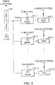
- FIG. 4 illustrates a chip having a plurality of pads 104_1, 104_2... 104_N, a plurality of I/O buffers 102_1, 102_2... 102_N, and one single bias circuit 106.
- each I/O buffer is equipped with an exclusive bias circuit that directly draws power for the corresponding pad, and N I/O buffers require N bias circuits. Power consumption due to the bias requirement is suppressed to 1/N times by the forgoing external bias circuit.
- any chip comprising an I/O buffer using the external bias circuit should be regarded as within the scope of the present invention.
Landscapes
- Engineering & Computer Science (AREA)
- Physics & Mathematics (AREA)
- Computer Hardware Design (AREA)
- Computing Systems (AREA)
- General Engineering & Computer Science (AREA)
- Mathematical Physics (AREA)
- Nonlinear Science (AREA)
- Microelectronics & Electronic Packaging (AREA)
- Power Engineering (AREA)
- Semiconductor Integrated Circuits (AREA)
- Logic Circuits (AREA)
- Amplifiers (AREA)
Abstract
Description
- The present invention relates to a chip with pad tracking.
- In some situations, a chip may not receive power even though the system power has been turned on. Current from the system power may be fed into the chip through the chip's pad. A pad-tracking design is required to block such a leakage path.
- However, the power consumed by such a pad-tracking design may increase with the number of pads of the chip. How to suppress the power consumption of the pad-tracking design is an important issue in the field of chip design.
- A chip with pad tracking is shown.
- A chip with pad tracking in accordance with an exemplary embodiment of the present invention has an input/output buffer (I/O buffer), a pad, and a bias circuit. The I/O buffer is powered by a first power and is coupled to the pad. The pad is coupled to the system power. The bias circuit generates a bias signal for the I/O buffer to block a leakage path within the I/O buffer when the system power is on and the first power is off. The bias circuit is a voltage divider which generates a divided voltage as the bias signal. In an exemplary embodiment, the bias circuit is powered by a second power that is independent from the first power and is not drawn from the pad. In exemplary embodiment, a power terminal of the bias circuit is coupled to an electrostatic discharging bus of the chip. The pad is coupled to the electrostatic discharging bus through a diode.
- Because the bias circuit of the present invention is power by an additional power or an electrostatic discharging bus, the bias circuit is an external design not bounded with an I/O buffer. The present invention proposes an external bias circuit for pad tracking of a chip.
- In an exemplary embodiment, the I/O buffer comprises a floating N-well pull-up string, and a pad-tracking circuit. According to the bias signal, the pad-tracking circuit couples the pad to a gate and a bulk of a leakage-blocking transistor of the floating N-well pull-up string. Accordingly, the leakage-blocking transistor is turned off, and the leakage path within the floating N-well pull-up string is broken.
- In an exemplary embodiment, the pad-tracking circuit comprises a p-type transistor coupled between the gate of the leakage-blocking transistor and the pad. The gate of the p-type transistor is controlled by the bias signal. The p-type transistor is turned on when the bias signal is at a proper voltage level.
- In an exemplary embodiment, the pad-tracking circuit comprises a p-type transistor coupled between the bulk of the leakage-blocking transistor and the pad. The gate of the p-type transistor is controlled by the bias signal. The p-type transistor is turned on when the bias signal is at a proper voltage level.
- The external bias circuit can be shared by the I/O buffers of the different pads.
- In another exemplary embodiment, a chip with pad tracking in accordance with an exemplary embodiment of the present invention has a plurality of pads, a plurality of I/O buffers, and a bias circuit shared by the different I/O buffers. Because only one bias circuit is required, power consumption is considerably reduced.
- A detailed description is given in the following embodiments with reference to the accompanying drawings.
- The present invention can be more fully understood by reading the subsequent detailed description and examples with references made to the accompanying drawings, wherein:
-
FIG. 1 illustrates achip 100 with pad tracking in accordance with an exemplary embodiment of the present invention; -
FIG. 2 illustrates the details of thebias circuit 106, the power-onsystem 108, the floating N-well pull-up string 110, and the pad-tracking circuit 112 in accordance with an exemplary embodiment of the present invention; -
FIG. 3 shows details about how to power thebias circuit 106 by an electrostatic discharging bus (EBUS) in accordance with an exemplary embodiment of the present invention; and -
FIG. 4 illustrates a chip having a plurality of pads 104_1, 104_2... 104_N, a plurality of I/O buffers 102_1, 102_2... 102_N, and just onesingle bias circuit 106. - The following description is made for the purpose of illustrating the general principles of the invention and should not be taken in a limiting sense. The scope of the invention is best determined by reference to the appended claims.
-
FIG. 1 illustrates achip 100 with pad tracking in accordance with an exemplary embodiment of the present invention. - The
chip 100 with pad tracking has an input/output buffer (I/O buffer) 102, apad 104, and abias circuit 106. The I/O buffer 102 powered by the chip's power VDIO1 is coupled to thepad 104, and thepad 104 is coupled to the system power VDIO2 (e.g., through a power-on system 108). In this case, thechip 100 is an overdriven device. The normal voltage level of the chip's power VDIO1 and the system power VDIO2 is 2∗VDDQ.FIG. 1 shows a situation that the system power VDIO2 has been turned on (VDI02 is 2∗VDDQ) but the chip's power VDIO1 has not been turned on yet (VDIO1 is 0 volts). - In
FIG. 1 , only the pull-up path of the I/O buffer 102 is shown. The pull-down path of the I/O buffer 102 is not shown inFIG. 1 for simplicity. The I/O buffer 102 includes a floating N-well pull-up string 110, and a pad-tracking circuit 112. The pad-tracking circuit 112 is biased by a bias signal Vmid generated by thebias circuit 106. According to the bias signal Vmid, the pad-tracking circuit 112 couples thepad 104 to the floating N-well pull-upstring 110. As shown, the pad level VPAD is coupled to the floating N-well pull-upstring 110 through the pad-tracking circuit 112 when the bias voltage Vmid is at the proper voltage level. Referring to the power situation shown inFIG. 1 wherein the system power VDIO2 is on (=2∗VDDQ) and the chip's power VDIO1 is off (= 0 volts), a leakage path within the I/O buffer 102 from the pad 104 (with VPAD at 2∗VDDQ) to the 0V VDIO1 is broken due to the pad level VPAD (=2∗VDDQ) supplied to the floating N-well pull-up string 110 (e.g., coupled to the gate of one transistor of the floating N-well pull-up string 110). The unnecessary current consumption is prevented. - The
bias circuit 106 is powered by another power VDI03. In the power situation shown inFIG. 1 wherein the system power VDIO2 is on (=2∗VDDQ) and the chip's power VDIO1 is off (= 0 volts), the power VDIO3 is on (≈2∗VDDQ). Note that the power VDIO3 is not directly drawn from the pad voltage VPAD. In an exemplary embodiment, VDIO3 is an additional power that is independent from the chip's power VDIO1 and is not drawn from the pad VPAD. In another exemplary embodiment, VDIO3 is provided by an electrostatic discharging bus (EBUS) of thechip 100. Thepad 104 is coupled to the electrostatic discharging bus (EBUS) through a diode. When the system power VDIO2 is turned on (=2∗VDDQ), thebias circuit 106 is powered by the electrostatic discharging bus (EBUS) that is at a voltage level near 2∗VDDQ. Thebias circuit 106 is a voltage divider which generates a divided voltage as the bias signal Vmid. For example, the bias voltage Vmid may be VDDQ, which is a proper voltage level to bias thepad tracking circuit 112. -
FIG. 2 illustrates the details of thebias circuit 106, the power-onsystem 108, the floating N-well pull-upstring 110, and the pad-tracking circuit 112 in accordance with an exemplary embodiment of the present invention. - The
bias circuit 106 is a voltage divider that uses two resistors R1 and R2 to divide the voltage (=2∗VDDQ) of the power VDIO3 to generate a divided voltage VDDQ as the bias signal Vmid. The power-onsystem 108 is represented by a resistor Rpull up. One transistor (e.g., a PMOS) P1 in the floating N-well pull-upstring 110 is used as a leakage-blocking transistor. The pad-tracking circuit 112 has a p-type transistor (e.g., a PMOS) P2 coupled between the gate of the leakage-blocking transistor P1 and thepad 104, and the gate of the p-type transistor P2 is controlled by the bias signal Vmid. The pad-tracking circuit 112 further has a p-type transistor (e.g., a PMOS) P3 coupled between the bulk of the leakage-blocking transistor P1 and thepad 104, and the gate of the p-type transistor P3 is controlled by the bias signal Vmid. When the system power VDIO2 is on (=2∗VDDQ) and the chip's power VDIO1 is off (= 0 volts), according to the bias signal Vmid (=VDDQ), the pad voltage VPAD (=2∗VDDQ) is coupled to the gate of the leakage-blocking transistor P1 through the turned-on p-type transistor P2, and is coupled to the bulk of the leakage-blocking transistor P1 through the turned-on p-type transistor P3. Thus, the leakage-blocking transistor P1 is turned off, and the leakage path from the VDIO2 to the VDIO1 through thepad 104 and the floating N-well pull-upstring 110 is broken. -
FIG. 3 details how to power thebias circuit 106 by an electrostatic discharging bus EBUS in accordance with an exemplary embodiment of the present invention. As shown, thepad 104 is coupled to the electrostatic discharging bus EBUS through adiode 302. When the system power VDIO2 coupled to thepad 104 is on (=2∗VDDQ), thediode 302 couples theoverdrive voltage level 2∗VDDQ to the electrostatic discharging bus EBUS, and thebias circuit 106 generates the divided voltage VDDQ as the bias voltage Vmid for the I/O buffer 102. - Because the
bias circuit 106 does not directly draw power from thepad 104, thebias circuit 106 is regarded as an external design not bounded within the I/O buffer 102. Thus, when a chip has multiple pads, the different I/O buffers of the different pads may share the same bias circuit. -
FIG. 4 illustrates a chip having a plurality of pads 104_1, 104_2... 104_N, a plurality of I/O buffers 102_1, 102_2... 102_N, and onesingle bias circuit 106. The bias signal Vmid (=VDDQ) generated by thesingle bias circuit 106 is dispatched to all I/O buffers 102_1, 102_2... 102_N to block all leakage paths within the I/O buffers 102_1, 102_2... 102_N when the system power VDIO2 is on (=2∗VDDQ) and the chip's power VDIO1 is off (= 0 volts). - Because just one
single bias circuit 106 is required in the pad tracking of the multiple pads 104_1, 104_2... 104_N, the power consumption due to the bias design is limited. In the conventional techniques, each I/O buffer is equipped with an exclusive bias circuit that directly draws power for the corresponding pad, and N I/O buffers require N bias circuits. Power consumption due to the bias requirement is suppressed to 1/N times by the forgoing external bias circuit. - Any chip comprising an I/O buffer using the external bias circuit (powered by an additional power that is independent from VDIO1 and is not drawn from any pad, or powered by an electrostatic discharging bus EBUS) should be regarded as within the scope of the present invention.
- While the invention has been described by way of example and in terms of the preferred embodiments, it should be understood that the invention is not limited to the disclosed embodiments. On the contrary, it is intended to cover various modifications and similar arrangements (as would be apparent to those skilled in the art).
Claims (15)
- A chip (100) with pad tracking, comprising:a first input/output buffer (102_1) and a first pad (104_1), wherein the first input/output buffer powered by a first power is coupled to the first pad, and the first pad is coupled to a system power (VDIO1);a second input/output buffer (102_2) and a second pad (104_2), wherein the second input/output buffer powered by the first power is coupled to the second pad, and the second pad is coupled to the system power; anda bias circuit (106), generating a bias signal which is dispatched to the first input/output buffer and the second input/output buffer to block a first leakage path within the first input/output buffer and a second leakage path within the second input/output buffer when the system power is on and the first power is off.
- The chip with pad tracking as claimed in claim 1, wherein:
the bias circuit is a voltage divider, which generates a divided voltage which serves as the bias signal to be dispatched to the first input/output buffer and the second input/output buffer both. - The chip with pad tracking as claimed in claim 2, wherein:
the bias circuit is powered by a second power (VDI03) that is independent from the first power and is not drawn from any of the first and second pads. - The chip with pad tracking as claimed in claim 2 or 3, further comprising:an electrostatic discharging bus (EBUS);a first diode; anda second diode;wherein:a power terminal of the bias circuit is coupled to the electrostatic discharging bus;the first pad is coupled to the electrostatic discharging bus through the first diode; andthe second pad is coupled to the electrostatic discharging bus through the second diode.
- The chip with pad tracking as claimed in any one of claims 2 to 4, wherein:the first input/output buffer comprises a first floating N-well pull-up string (110), and a first pad-tracking circuit (112);according to the bias signal, the first pad-tracking circuit couples the first pad to a gate and a bulk of a first leakage-blocking transistor (P1) of the first floating N-well pull-up string;the second input/output buffer comprises a second floating N-well pull-up string, and a second pad-tracking circuit; andaccording to the bias signal, the second pad-tracking circuit couples the second pad to a gate and a bulk of a second leakage-blocking transistor of the second floating N-well pull-up string.
- The chip with pad tracking as claimed in claim 5, wherein:the first pad-tracking circuit comprises a first p-type transistor (P2) coupled between the gate of the first leakage-blocking transistor (P1) and the first pad, and a gate of the first p-type transistor is controlled by the bias signal; andthe second pad-tracking circuit comprises a second p-type transistor coupled between the gate of the second leakage-blocking transistor and the first pad, and a gate of the second p-type transistor is controlled by the bias signal.
- The chip with pad tracking as claimed in claim 5 or 6, wherein:the first pad-tracking circuit comprises a third p-type transistor (P3) coupled between the bulk of the first leakage-blocking transistor (P1) and the first pad, and a gate of the third p-type transistor is controlled by the bias signal; andthe second pad-tracking circuit comprises a fourth p-type transistor coupled between the bulk of the second leakage-blocking transistor and the second pad, and a gate of the fourth p-type transistor is controlled by the bias signal.
- A chip with pad tracking, comprising:an input/output buffer (102) and a pad (104), wherein the input/output buffer powered by a first power is coupled to the pad, and the pad is coupled to a system power (VDIO1);a bias circuit (106), generating a bias signal to be transferred to the input/output buffer to block a leakage path within the input/output buffer when the system power is on and the first power is off,wherein:the bias circuit is a voltage divider which generates a divided voltage as the bias signal; andthe bias circuit is powered by a second power (VDI03) that is independent from the first power and is not drawn from the pad.
- The chip with pad tracking as claimed in claim 8, wherein:the input/output buffer comprises a floating N-well pull-up string (110), and a pad-tracking circuit (112); andaccording to the bias signal, the pad-tracking circuit couples the pad to a gate and a bulk of a leakage-blocking transistor (P1) of the floating N-well pull-up string.
- The chip with pad tracking as claimed in claim 9, wherein:
the pad-tracking circuit comprises a p-type transistor (P2) coupled between the gate of the leakage-blocking transistor and the pad, and a gate of the p-type transistor is controlled by the bias signal. - The chip with pad tracking as claimed in claim 9 or 10, wherein:
the pad-tracking circuit comprises a p-type transistor (P3) coupled between the bulk of the leakage-blocking transistor (P1) and the pad, and a gate of the p-type transistor (P3) is controlled by the bias signal. - A chip with pad tracking, comprising:an input/output buffer (102) and a pad (104), wherein the input/output buffer powered by a first power is coupled to the pad, and the pad is coupled to a system power (VDIO1);an electrostatic discharging bus (EBUS) and a diode (302), wherein the diode couples the pad to the electrostatic discharging bus;a bias circuit (106), generating a bias signal to be transferred to the input/output buffer to block a leakage path within the input/output buffer when the system power is on and the first power is off,wherein:the bias circuit is a voltage divider which generates a divided voltage as the bias signal; anda power terminal of the bias circuit is coupled to the electrostatic discharging bus.
- The chip with pad tracking as claimed in claim 12, wherein:the input/output buffer comprises a floating N-well pull-up string (110), and a pad-tracking circuit (112); andaccording to the bias signal, the pad-tracking circuit couples the pad to a gate and a bulk of a leakage-blocking transistor (P1) of the floating N-well pull-up string.
- The chip with pad tracking as claimed in claim 13, wherein:
the pad-tracking circuit comprises a p-type transistor (P2) coupled between the gate of the leakage-blocking transistor (P1) and the pad, and a gate of the p-type transistor (P2) is controlled by the bias signal. - The chip with pad tracking as claimed in claim 13 or 14, wherein:
the pad-tracking circuit comprises a p-type transistor (P3) coupled between the bulk of the leakage-blocking transistor (P1) and the pad, and a gate of the p-type transistor (P3) is controlled by the bias signal.
Applications Claiming Priority (2)
| Application Number | Priority Date | Filing Date | Title |
|---|---|---|---|
| US202163171643P | 2021-04-07 | 2021-04-07 | |
| US17/580,952 US11716073B2 (en) | 2021-04-07 | 2022-01-21 | Chip with pad tracking |
Publications (1)
| Publication Number | Publication Date |
|---|---|
| EP4072019A1 true EP4072019A1 (en) | 2022-10-12 |
Family
ID=80683626
Family Applications (1)
| Application Number | Title | Priority Date | Filing Date |
|---|---|---|---|
| EP22160628.8A Withdrawn EP4072019A1 (en) | 2021-04-07 | 2022-03-07 | A chip with pad tracking |
Country Status (4)
| Country | Link |
|---|---|
| US (1) | US11716073B2 (en) |
| EP (1) | EP4072019A1 (en) |
| CN (1) | CN115207893B (en) |
| TW (1) | TWI804250B (en) |
Families Citing this family (2)
| Publication number | Priority date | Publication date | Assignee | Title |
|---|---|---|---|---|
| CN119512290A (en) * | 2023-08-23 | 2025-02-25 | 联发科技(新加坡)私人有限公司 | A dynamic bias voltage circuit and integrated circuit |
| TWI912822B (en) * | 2024-07-05 | 2026-01-21 | 立積電子股份有限公司 | Electrostatic discharge protection device |
Citations (2)
| Publication number | Priority date | Publication date | Assignee | Title |
|---|---|---|---|---|
| EP3451537A1 (en) * | 2017-08-29 | 2019-03-06 | ams AG | High-voltage output driver for a sensor device with reverse current blocking |
| EP3731414A1 (en) * | 2019-04-26 | 2020-10-28 | STMicroelectronics (Rousset) SAS | Association of transistors in series |
Family Cites Families (10)
| Publication number | Priority date | Publication date | Assignee | Title |
|---|---|---|---|---|
| KR100328809B1 (en) * | 1999-07-22 | 2002-03-14 | 윤종용 | Semiconductor memory device with wafer level test function |
| TW473979B (en) | 2001-03-28 | 2002-01-21 | Silicon Integrated Sys Corp | ESD protection circuit for mixed-voltage I/O by using stacked NMOS transistors with substrate triggering technique |
| US6970336B2 (en) * | 2003-10-10 | 2005-11-29 | Freescale Semiconductor, Inc. | Electrostatic discharge protection circuit and method of operation |
| US7394291B2 (en) | 2005-12-26 | 2008-07-01 | Stmicroelectronics Pvt. Ltd. | High voltage tolerant output buffer |
| US7986171B2 (en) * | 2008-10-21 | 2011-07-26 | Himax Technologies Limited | Mixed-voltage I/O buffer |
| US8179160B1 (en) * | 2010-12-17 | 2012-05-15 | Texas Instruments Incorporated | Input-output (I/O) circuit supporting multiple I/O logic-level swings |
| WO2016038748A1 (en) | 2014-09-12 | 2016-03-17 | 株式会社東芝 | Storage device |
| TWI653831B (en) * | 2018-04-12 | 2019-03-11 | 瑞昱半導體股份有限公司 | Buffer circuit |
| US20200243512A1 (en) * | 2019-01-28 | 2020-07-30 | Stmicroelectronics International N.V. | Nmos transistor with bulk dynamically coupled to drain |
| US11726943B2 (en) * | 2020-03-06 | 2023-08-15 | Apogee Semiconductor, Inc. | Circuits and methods for enabling redundancy in an electronic system employing cold-sparing |
-
2022
- 2022-01-21 US US17/580,952 patent/US11716073B2/en active Active
- 2022-03-04 CN CN202210209751.9A patent/CN115207893B/en active Active
- 2022-03-07 EP EP22160628.8A patent/EP4072019A1/en not_active Withdrawn
- 2022-03-25 TW TW111111223A patent/TWI804250B/en active
Patent Citations (2)
| Publication number | Priority date | Publication date | Assignee | Title |
|---|---|---|---|---|
| EP3451537A1 (en) * | 2017-08-29 | 2019-03-06 | ams AG | High-voltage output driver for a sensor device with reverse current blocking |
| EP3731414A1 (en) * | 2019-04-26 | 2020-10-28 | STMicroelectronics (Rousset) SAS | Association of transistors in series |
Also Published As
| Publication number | Publication date |
|---|---|
| TW202241064A (en) | 2022-10-16 |
| TWI804250B (en) | 2023-06-01 |
| US20220329232A1 (en) | 2022-10-13 |
| CN115207893A (en) | 2022-10-18 |
| CN115207893B (en) | 2026-04-24 |
| US11716073B2 (en) | 2023-08-01 |
Similar Documents
| Publication | Publication Date | Title |
|---|---|---|
| US6147540A (en) | High voltage input buffer made by a low voltage process and having a self-adjusting trigger point | |
| KR100295316B1 (en) | Low voltage input and output circuit with overvoltage protection | |
| US7394706B2 (en) | Semiconductor integrated circuit device | |
| US8344760B2 (en) | Input/output buffer circuit | |
| US6724226B2 (en) | Signal transmission circuit capable of tolerating high-voltage input signal | |
| US20050046449A1 (en) | Voltage mismatch tolerant input/output buffer | |
| US11716073B2 (en) | Chip with pad tracking | |
| US6144221A (en) | Voltage tolerant interface circuit | |
| US6335637B1 (en) | Two-supply protection circuit | |
| US10867989B2 (en) | Driving circuit having electrostatic discharge protection | |
| US6064231A (en) | CMOS input buffer protection circuit | |
| US7180331B2 (en) | Voltage tolerant structure for I/O cells | |
| US5914617A (en) | Output driver for sub-micron CMOS | |
| US10622976B2 (en) | Schmitt trigger circuit | |
| US6788107B2 (en) | Variable voltage tolerant input/output circuit | |
| US6621299B1 (en) | Control circuit for power | |
| US20040001551A1 (en) | Data transmission circuit and method for reducing leakage current | |
| CN103529715B (en) | current delivery circuit | |
| US20050128670A1 (en) | Input/output buffer protection circuit | |
| KR100282228B1 (en) | Data output buffer | |
| US20080049533A1 (en) | Supply voltage distribution system with reduced resistance for semiconductor devices | |
| US20050281074A1 (en) | Input return path based on VDDQ/VSSQ | |
| JPH07106517A (en) | Semiconductor device and semiconductor memory device | |
| KR20050025451A (en) | Voltage down converter circuit | |
| JP2002118453A (en) | Semiconductor integrated circuit |
Legal Events
| Date | Code | Title | Description |
|---|---|---|---|
| PUAI | Public reference made under article 153(3) epc to a published international application that has entered the european phase |
Free format text: ORIGINAL CODE: 0009012 |
|
| STAA | Information on the status of an ep patent application or granted ep patent |
Free format text: STATUS: THE APPLICATION HAS BEEN PUBLISHED |
|
| AK | Designated contracting states |
Kind code of ref document: A1 Designated state(s): AL AT BE BG CH CY CZ DE DK EE ES FI FR GB GR HR HU IE IS IT LI LT LU LV MC MK MT NL NO PL PT RO RS SE SI SK SM TR |
|
| STAA | Information on the status of an ep patent application or granted ep patent |
Free format text: STATUS: REQUEST FOR EXAMINATION WAS MADE |
|
| 17P | Request for examination filed |
Effective date: 20230412 |
|
| RBV | Designated contracting states (corrected) |
Designated state(s): AL AT BE BG CH CY CZ DE DK EE ES FI FR GB GR HR HU IE IS IT LI LT LU LV MC MK MT NL NO PL PT RO RS SE SI SK SM TR |
|
| P01 | Opt-out of the competence of the unified patent court (upc) registered |
Effective date: 20230607 |
|
| STAA | Information on the status of an ep patent application or granted ep patent |
Free format text: STATUS: EXAMINATION IS IN PROGRESS |
|
| 17Q | First examination report despatched |
Effective date: 20240711 |
|
| STAA | Information on the status of an ep patent application or granted ep patent |
Free format text: STATUS: THE APPLICATION HAS BEEN WITHDRAWN |
|
| 18W | Application withdrawn |
Effective date: 20241108 |