EP4071834A1 - Method of processing inconsistencies in solar cell devices and devices formed thereby - Google Patents
Method of processing inconsistencies in solar cell devices and devices formed thereby Download PDFInfo
- Publication number
- EP4071834A1 EP4071834A1 EP22175903.8A EP22175903A EP4071834A1 EP 4071834 A1 EP4071834 A1 EP 4071834A1 EP 22175903 A EP22175903 A EP 22175903A EP 4071834 A1 EP4071834 A1 EP 4071834A1
- Authority
- EP
- European Patent Office
- Prior art keywords
- inconsistency
- solar cell
- conductive line
- inconsistencies
- semiconductor substrate
- Prior art date
- Legal status (The legal status is an assumption and is not a legal conclusion. Google has not performed a legal analysis and makes no representation as to the accuracy of the status listed.)
- Pending
Links
- 238000000034 method Methods 0.000 title claims abstract description 102
- 238000012545 processing Methods 0.000 title claims abstract description 7
- 239000000758 substrate Substances 0.000 claims abstract description 86
- 239000004065 semiconductor Substances 0.000 claims abstract description 67
- 239000000463 material Substances 0.000 claims abstract description 39
- 230000008021 deposition Effects 0.000 claims abstract description 31
- 238000000151 deposition Methods 0.000 claims description 83
- 229910052751 metal Inorganic materials 0.000 claims description 58
- 239000002184 metal Substances 0.000 claims description 56
- 229920002120 photoresistant polymer Polymers 0.000 claims description 36
- 230000005855 radiation Effects 0.000 claims description 20
- PXHVJJICTQNCMI-UHFFFAOYSA-N Nickel Chemical compound [Ni] PXHVJJICTQNCMI-UHFFFAOYSA-N 0.000 claims description 12
- 150000002739 metals Chemical class 0.000 claims description 8
- 238000009713 electroplating Methods 0.000 claims description 6
- 229910052759 nickel Inorganic materials 0.000 claims description 6
- 239000002245 particle Substances 0.000 claims description 6
- RYGMFSIKBFXOCR-UHFFFAOYSA-N Copper Chemical compound [Cu] RYGMFSIKBFXOCR-UHFFFAOYSA-N 0.000 claims description 5
- BQCADISMDOOEFD-UHFFFAOYSA-N Silver Chemical compound [Ag] BQCADISMDOOEFD-UHFFFAOYSA-N 0.000 claims description 5
- 229910052782 aluminium Inorganic materials 0.000 claims description 5
- XAGFODPZIPBFFR-UHFFFAOYSA-N aluminium Chemical compound [Al] XAGFODPZIPBFFR-UHFFFAOYSA-N 0.000 claims description 5
- 229910052802 copper Inorganic materials 0.000 claims description 5
- 239000010949 copper Substances 0.000 claims description 5
- PCHJSUWPFVWCPO-UHFFFAOYSA-N gold Chemical compound [Au] PCHJSUWPFVWCPO-UHFFFAOYSA-N 0.000 claims description 5
- 229910052737 gold Inorganic materials 0.000 claims description 5
- 239000010931 gold Substances 0.000 claims description 5
- 229910052709 silver Inorganic materials 0.000 claims description 5
- 239000004332 silver Substances 0.000 claims description 5
- 238000005137 deposition process Methods 0.000 claims description 4
- 229920000642 polymer Polymers 0.000 claims description 4
- 210000004027 cell Anatomy 0.000 description 73
- 230000008569 process Effects 0.000 description 44
- 239000004020 conductor Substances 0.000 description 10
- 239000000976 ink Substances 0.000 description 7
- 239000013078 crystal Substances 0.000 description 6
- 229910001218 Gallium arsenide Inorganic materials 0.000 description 5
- 238000001514 detection method Methods 0.000 description 5
- 230000004048 modification Effects 0.000 description 5
- 238000012986 modification Methods 0.000 description 5
- 229910045601 alloy Inorganic materials 0.000 description 4
- 239000000956 alloy Substances 0.000 description 4
- 238000001152 differential interference contrast microscopy Methods 0.000 description 4
- 238000009792 diffusion process Methods 0.000 description 4
- 239000011810 insulating material Substances 0.000 description 4
- 238000005424 photoluminescence Methods 0.000 description 4
- 238000007639 printing Methods 0.000 description 4
- 238000013459 approach Methods 0.000 description 3
- 238000005530 etching Methods 0.000 description 3
- 238000007689 inspection Methods 0.000 description 3
- 238000001465 metallisation Methods 0.000 description 3
- 238000000059 patterning Methods 0.000 description 3
- XUIMIQQOPSSXEZ-UHFFFAOYSA-N Silicon Chemical compound [Si] XUIMIQQOPSSXEZ-UHFFFAOYSA-N 0.000 description 2
- 230000004075 alteration Effects 0.000 description 2
- 230000004888 barrier function Effects 0.000 description 2
- 230000000593 degrading effect Effects 0.000 description 2
- 238000005868 electrolysis reaction Methods 0.000 description 2
- 238000005516 engineering process Methods 0.000 description 2
- 230000008020 evaporation Effects 0.000 description 2
- 238000001704 evaporation Methods 0.000 description 2
- 229910052732 germanium Inorganic materials 0.000 description 2
- GNPVGFCGXDBREM-UHFFFAOYSA-N germanium atom Chemical compound [Ge] GNPVGFCGXDBREM-UHFFFAOYSA-N 0.000 description 2
- 239000007788 liquid Substances 0.000 description 2
- 238000004519 manufacturing process Methods 0.000 description 2
- 239000007769 metal material Substances 0.000 description 2
- 239000011224 oxide ceramic Substances 0.000 description 2
- 229910052574 oxide ceramic Inorganic materials 0.000 description 2
- 229910052710 silicon Inorganic materials 0.000 description 2
- 239000010703 silicon Substances 0.000 description 2
- 229910001316 Ag alloy Inorganic materials 0.000 description 1
- 229910000838 Al alloy Inorganic materials 0.000 description 1
- 229910001020 Au alloy Inorganic materials 0.000 description 1
- 229910000881 Cu alloy Inorganic materials 0.000 description 1
- 229910000990 Ni alloy Inorganic materials 0.000 description 1
- 239000004952 Polyamide Substances 0.000 description 1
- 239000004642 Polyimide Substances 0.000 description 1
- 230000015572 biosynthetic process Effects 0.000 description 1
- 238000012993 chemical processing Methods 0.000 description 1
- 230000007547 defect Effects 0.000 description 1
- 239000002019 doping agent Substances 0.000 description 1
- 230000000694 effects Effects 0.000 description 1
- 238000005401 electroluminescence Methods 0.000 description 1
- 239000003353 gold alloy Substances 0.000 description 1
- 238000007641 inkjet printing Methods 0.000 description 1
- 238000005259 measurement Methods 0.000 description 1
- 239000002105 nanoparticle Substances 0.000 description 1
- 230000003287 optical effect Effects 0.000 description 1
- 230000003647 oxidation Effects 0.000 description 1
- 238000007254 oxidation reaction Methods 0.000 description 1
- 229920002647 polyamide Polymers 0.000 description 1
- 229920001721 polyimide Polymers 0.000 description 1
- 239000002861 polymer material Substances 0.000 description 1
- 230000006798 recombination Effects 0.000 description 1
- 238000005215 recombination Methods 0.000 description 1
- 230000035945 sensitivity Effects 0.000 description 1
- 239000002904 solvent Substances 0.000 description 1
- 238000012360 testing method Methods 0.000 description 1
- 238000012876 topography Methods 0.000 description 1
Images



Classifications
-
- H—ELECTRICITY
- H10—SEMICONDUCTOR DEVICES; ELECTRIC SOLID-STATE DEVICES NOT OTHERWISE PROVIDED FOR
- H10F—INORGANIC SEMICONDUCTOR DEVICES SENSITIVE TO INFRARED RADIATION, LIGHT, ELECTROMAGNETIC RADIATION OF SHORTER WAVELENGTH OR CORPUSCULAR RADIATION
- H10F77/00—Constructional details of devices covered by this subclass
- H10F77/70—Surface textures, e.g. pyramid structures
- H10F77/707—Surface textures, e.g. pyramid structures of the substrates or of layers on substrates, e.g. textured ITO layer on a glass substrate
-
- H—ELECTRICITY
- H02—GENERATION; CONVERSION OR DISTRIBUTION OF ELECTRIC POWER
- H02S—GENERATION OF ELECTRIC POWER BY CONVERSION OF INFRARED RADIATION, VISIBLE LIGHT OR ULTRAVIOLET LIGHT, e.g. USING PHOTOVOLTAIC [PV] MODULES
- H02S50/00—Monitoring or testing of PV systems, e.g. load balancing or fault identification
- H02S50/10—Testing of PV devices, e.g. of PV modules or single PV cells
-
- H—ELECTRICITY
- H10—SEMICONDUCTOR DEVICES; ELECTRIC SOLID-STATE DEVICES NOT OTHERWISE PROVIDED FOR
- H10F—INORGANIC SEMICONDUCTOR DEVICES SENSITIVE TO INFRARED RADIATION, LIGHT, ELECTROMAGNETIC RADIATION OF SHORTER WAVELENGTH OR CORPUSCULAR RADIATION
- H10F71/00—Manufacture or treatment of devices covered by this subclass
-
- H—ELECTRICITY
- H10—SEMICONDUCTOR DEVICES; ELECTRIC SOLID-STATE DEVICES NOT OTHERWISE PROVIDED FOR
- H10F—INORGANIC SEMICONDUCTOR DEVICES SENSITIVE TO INFRARED RADIATION, LIGHT, ELECTROMAGNETIC RADIATION OF SHORTER WAVELENGTH OR CORPUSCULAR RADIATION
- H10F71/00—Manufacture or treatment of devices covered by this subclass
- H10F71/10—Manufacture or treatment of devices covered by this subclass the devices comprising amorphous semiconductor material
-
- H—ELECTRICITY
- H10—SEMICONDUCTOR DEVICES; ELECTRIC SOLID-STATE DEVICES NOT OTHERWISE PROVIDED FOR
- H10F—INORGANIC SEMICONDUCTOR DEVICES SENSITIVE TO INFRARED RADIATION, LIGHT, ELECTROMAGNETIC RADIATION OF SHORTER WAVELENGTH OR CORPUSCULAR RADIATION
- H10F71/00—Manufacture or treatment of devices covered by this subclass
- H10F71/137—Batch treatment of the devices
-
- H—ELECTRICITY
- H10—SEMICONDUCTOR DEVICES; ELECTRIC SOLID-STATE DEVICES NOT OTHERWISE PROVIDED FOR
- H10F—INORGANIC SEMICONDUCTOR DEVICES SENSITIVE TO INFRARED RADIATION, LIGHT, ELECTROMAGNETIC RADIATION OF SHORTER WAVELENGTH OR CORPUSCULAR RADIATION
- H10F77/00—Constructional details of devices covered by this subclass
- H10F77/20—Electrodes
- H10F77/206—Electrodes for devices having potential barriers
- H10F77/211—Electrodes for devices having potential barriers for photovoltaic cells
-
- H—ELECTRICITY
- H10—SEMICONDUCTOR DEVICES; ELECTRIC SOLID-STATE DEVICES NOT OTHERWISE PROVIDED FOR
- H10F—INORGANIC SEMICONDUCTOR DEVICES SENSITIVE TO INFRARED RADIATION, LIGHT, ELECTROMAGNETIC RADIATION OF SHORTER WAVELENGTH OR CORPUSCULAR RADIATION
- H10F77/00—Constructional details of devices covered by this subclass
- H10F77/93—Interconnections
- H10F77/933—Interconnections for devices having potential barriers
- H10F77/935—Interconnections for devices having potential barriers for photovoltaic devices or modules
- H10F77/939—Output lead wires or elements
-
- Y—GENERAL TAGGING OF NEW TECHNOLOGICAL DEVELOPMENTS; GENERAL TAGGING OF CROSS-SECTIONAL TECHNOLOGIES SPANNING OVER SEVERAL SECTIONS OF THE IPC; TECHNICAL SUBJECTS COVERED BY FORMER USPC CROSS-REFERENCE ART COLLECTIONS [XRACs] AND DIGESTS
- Y02—TECHNOLOGIES OR APPLICATIONS FOR MITIGATION OR ADAPTATION AGAINST CLIMATE CHANGE
- Y02E—REDUCTION OF GREENHOUSE GAS [GHG] EMISSIONS, RELATED TO ENERGY GENERATION, TRANSMISSION OR DISTRIBUTION
- Y02E10/00—Energy generation through renewable energy sources
- Y02E10/50—Photovoltaic [PV] energy
-
- Y—GENERAL TAGGING OF NEW TECHNOLOGICAL DEVELOPMENTS; GENERAL TAGGING OF CROSS-SECTIONAL TECHNOLOGIES SPANNING OVER SEVERAL SECTIONS OF THE IPC; TECHNICAL SUBJECTS COVERED BY FORMER USPC CROSS-REFERENCE ART COLLECTIONS [XRACs] AND DIGESTS
- Y02—TECHNOLOGIES OR APPLICATIONS FOR MITIGATION OR ADAPTATION AGAINST CLIMATE CHANGE
- Y02P—CLIMATE CHANGE MITIGATION TECHNOLOGIES IN THE PRODUCTION OR PROCESSING OF GOODS
- Y02P70/00—Climate change mitigation technologies in the production process for final industrial or consumer products
- Y02P70/50—Manufacturing or production processes characterised by the final manufactured product
Definitions
- the present disclosure is directed to methods of making wiring for solar cells on semiconductor substrates comprising inconsistencies, and to devices formed by the methods.
- FIG. 1 shows an example of a solar cell device 8 formed on a semiconductor substrate 10. As shown in FIG.
- semiconductor substrate 10 includes a support substrate 10a comprising germanium or silicon, a III/V single crystal device layer 10b (e.g., GaAs and/or InGaP) and front wiring 12.
- Semiconductor substrate 10 can have inconsistencies 14 and 16, as indicated. Inconsistency 14 is on the semiconductor substrate 10, but does not contact the front wiring 12 and thus would have little or no impact on performance. Inconsistency 16, however, is under a grid line and thus can potentially degrade solar cell performance. Inconsistencies that contact any part of the front wiring 12 may potentially degrade performance, including inconsistencies positioned under the bus bars 18, contact regions 20 or grid lines 22.
- FIG. 2 shows front wiring 12 on semiconductor substrate 10 having inconsistencies 14, 16a and 16b.
- the inconsistencies may come in a variety of types and from a variety of sources.
- One type of inconsistency 16a is in the form of a particle, such as a particle that has fallen during the deposition of the solar cell material, leading to a tall, non-planar surface feature that may potentially increase the resistance of any wiring formed thereon.
- Another inconsistency 16b can occur as a no growth region that appears as a hole in the semiconductor substrate, which can potentially increase resistance and/or cause an electrical short between active regions of the device, thereby degrading device performance.
- One common approach employs a lift-off technique to pattern metal lines.
- This process includes forming a patterned polymer lift-off mask on the semiconductor substrate.
- the lift-off mask is patterned for forming a desired solar cell wiring configuration using techniques well known in the art.
- the patterned lift-off mask has gaps exposing underlying portions of the substrate.
- a metal layer is blanket deposited from a directional process, such as evaporation, on the patterned lift-off mask and on exposed areas of the semiconductor substrate.
- the device is then soaked in solvents that "lift off” the patterned lift-off mask and overlying metal layers, while leaving metal not formed on the lift-off mask on the semiconductor substrate to form the wiring.
- metal is selectively deposited by electrolysis (also referred to herein as electroplating), in areas of the substrate that are exposed through the patterned mask, but not on the patterned mask itself.
- electrolysis also referred to herein as electroplating
- the patterned mask can then be removed and the selectively deposited metal remains as the conductive wiring.
- Other known processes for forming front wiring include first blanket depositing a metal layer using any suitable process, such as by evaporation or electroplating, and then patterning the metal layer using well known photolithographic techniques.
- photolithographic techniques can include depositing and developing a photoresist layer to form a pattered photoresist on the metal layer.
- the metal layer can then be patterned by removing the areas of the metal not protected by the patterned photoresist using well known etching processes. Following etching, the patterned photoresist is then removed to leave the patterned metal wiring on the substrate.
- the processes described above for forming front wiring on solar cells include the formation of a photoresist pattern.
- forming such a photoresist pattern generally involves exposing the photoresist to radiation through a photomask.
- photomasks require much time and expense to fabricate, and are repeatedly used to form essentially the same photoresist patterns to mass produce many thousands or millions of the same solar cell devices. Because the photomasks are not easily modified, the photoresist pattern cannot be readily modified to fabricate different front wiring patterns for individual devices.
- the present disclosure is directed to a method of processing a solar cell device.
- the method comprises detecting at least one inconsistency at a surface of a semiconductor substrate having a solar cell active region formed therein.
- a deposition pattern is determined based on the location of the at least one inconsistency.
- a material is selectively deposited on the substrate according to the deposition pattern.
- the present disclosure is also directed to a solar cell device.
- the solar cell device comprises at least one inconsistency at a surface of a semiconductor substrate having a solar cell active region formed therein.
- a conductive line is configured to avoid the at least one inconsistency.
- the present disclosure is further directed to a solar cell device.
- the solar cell device comprises at least one inconsistency at a surface of a semiconductor substrate having a solar cell active region formed therein.
- a front wiring is on the surface of the semiconductor substrate for collecting electrical current produced by the solar cell device.
- the front wiring comprises a conductive line positioned over one or more of the at least one inconsistencies.
- the solar cell device further comprises a patterned insulating layer separating the conductive line from the one or more inconsistencies.
- solar cells are formed using semiconductor substrates that may include surface inconsistencies.
- the present disclosure is directed to a method of processing a solar cell device that can ameliorate certain problems associated with forming conductive wiring on the inconsistencies.
- inconsistencies on the semiconductor device are located.
- the conductive wiring is then formed to avoid the inconsistencies.
- insulating layers can be used to encapsulate and/or fill the inconsistencies prior to forming the wiring, thereby separating the wiring from the inconsistencies.
- the disclosed methods can allow for improved current gathering by the wiring on the solar cell, potentially improve device yield and/or provide for increased output power of the solar cell by modifying and/or tailoring the wiring on the solar cell device.
- FIG. 3 shows an example process flow of the method.
- the method comprises detecting and determining the location of at least one inconsistency at a surface of a semiconductor substrate having a solar cell active region formed therein.
- inconsistency means any surface defect, non-planar surface feature or other surface irregularity that can cause shorting and/or increase resistance of the front wiring 12 if the front wiring 12 is formed thereon compared to the resistance of the wiring if the inconsistency were not present. Examples of such inconsistencies are discussed above with respect to FIG. 2 . Techniques and apparatuses for detecting and locating inconsistencies are well known in the art and are discussed in more detail below.
- a deposition pattern is determined based on the location of the inconsistency, as at process element 32. Selective deposition techniques can then be employed to selectively deposit a material on the substrate according to the determined deposition pattern, as at process element 34.
- semiconductor substrate 10 can comprise any semiconductor material suitable for solar cell device fabrication.
- the semiconductor substrate can include a support substrate 10a comprising germanium single crystal or silicon single crystal.
- One or more III/V single crystal materials such as GaAs and/or InGaP, is epitaxially grown on the support substrate 10a.
- the III/V material can include multiple layers, such as a III/V single crystal device layer 10b comprising, for example, InGaP, in which a top solar cell is formed; and a III/V single crystal cap layer 10c comprising, for example, GaAs, that can reduce contact resistance and surface recombination, as is well known in the art.
- the semiconductor substrate 10 can be doped with one or more n-type or p-type dopants to form at least one active region of the solar cell, which may comprise a p-n junction as is well known in the art.
- Exemplary active regions 64a and 64b are shown in FIG. 5 , although any suitable type or number of active regions can be employed.
- the semiconductor substrate 10 on which the wiring scheme is to be implemented is scanned for inconsistencies 14,16. All or a portion of the semiconductor substrate 10 can be scanned. If upon scanning the semiconductor substrate a inconsistency is found, the position of the inconsistency on the semiconductor substrate 10 is determined. Detecting a inconsistency at a surface of the semiconductor substrate can be carried out using any suitable inconsistency detection system. Inconsistency detection systems are available for scanning and locating inconsistencies on semiconductor substrates. Examples of suitable detection systems include the ICOS WI-2280 Series, the Candela CSxx and CS9920 Series, the Surfscan Series all of which are made by KLA Tencor of Milpitas, California. Another example is the AWX TM Series made by Rudolph Technologies Inc., of Flanders, New Jersey.
- Suitable detection systems can utilize reflected light, transmitted light, photoluminescence, electroluminescence or combinations thereof to detect inconsistencies.
- photoluminescence light emitted from the top cell of the solar cell device can potentially be used for detecting inconsistencies.
- a GaAs cap layer can absorb the light used to excite the InGaP device layer and will absorb the photoluminescence exciting the material.
- the GaAs cap can be made relatively thin, such as, for example, about 5 nm to about 200 nm, to achieve photoluminescence inspection.
- Differential interference contrast microscopy also known as Nomarski interference contrast or Nomarski microscopy can also be employed during inconsistency detection to increase contrast.
- Differential interference contrast microscopy employs an optical microscope with polarizers arranged to have increased sensitivity to height changes on a sample, which increases contract and visibility of inconsistencies, as is well known in the art.
- determining a deposition pattern based on the location of the inconsistency can optionally comprise providing an initial wiring scheme for the solar cell device.
- the initial wiring scheme can comprise any desired pattern for forming the wiring of a solar cell device being manufactured.
- an initial wiring scheme could comprise the pattern for depositing front wiring 12 on the solar cell device 8, as shown in FIG. 1 .
- the initial wiring scheme can be provided in any suitable manner, such as a set of software instructions that are compatible for guiding a printing apparatus for purposes of selectively depositing materials to form the desired pattern for front wiring 12 on the solar cell device 8.
- One of ordinary skill in the art would readily be able to provide a suitable initial wiring scheme, given the present disclosure.
- avoiding the inconsistency can reduce the risk of shorting and or avoid an undesirable increase in resistance of the front wiring, thereby potentially providing for improved current gathering by the wiring on the solar cell, improved device yield and/or increased output power of the solar cell.
- FIG. 4 shows an example deposition pattern in which the initial wiring scheme for front wiring 12 of FIG. 1 has been modified so that conductive line 24 avoids inconsistency 16.
- the modified wiring scheme comprises a conductive line 24 that circumvents the inconsistency so that the conductive line 24 is positioned proximate to, but not over, the inconsistency.
- proximate to in the context of positioning a conductive line to avoid a inconsistency is defined herein to be any distance that will cause the conductive line to avoid the inconsistency while not overlapping adjacent conductive lines.
- the conductive line can be positioned so that at its closest point to the inconsistency, it is positioned at a distance of from 0.001 microns to 5 microns from the inconsistency, such as 0.01 microns to 2 microns.
- the modification can be made to any portion of the initial wiring scheme that may be positioned on a inconsistency, such as bus bar 18, contact region 20 or a grid line 22, all of which may be referred to herein as a conductive line 24.
- the deposition pattern can be determined as described above, any other suitable technique for determining a deposition pattern that avoids the inconsistencies can be employed.
- any suitable selective deposition techniques can be used to deposit a material on the semiconductor substrate using the deposition pattern as a guide.
- the term "on” as used herein does not require direct physical contact and thus allows for intervening layers between the semiconductor substrate and the deposition pattern formed on the semiconductor substrate. Further, anytime the term “on” is employed herein to describe a relationship between layers, direct physical contact is contemplated as a possible option. The term “directly on” is defined to mean that direct physical contact is made.
- the conductive wiring itself is selectively deposited on the semiconductor substrate 10 in the determined deposition pattern.
- a mask pattern can be selectively deposited and used to form the conductive lines in the desired deposition pattern.
- any suitable conventional or later developed method for selectively depositing conductive lines can be employed.
- a conductive ink can be selectively deposited to form conductive lines using an inkjet print head, as is well known in the art.
- Still other techniques are known for selectively depositing various conductive materials, including micro- or nano-sized materials that may be dry, in a paste, suspended in a liquid, or are a liquid.
- the resulting conductive lines can comprise any suitable conductive material, such as one or more metals selected from aluminum, gold, silver, copper and nickel, which can be selectively deposited.
- suitable conductive material such as one or more metals selected from aluminum, gold, silver, copper and nickel, which can be selectively deposited.
- the use of the term "comprise” here is meant to include both pure or substantially pure materials, such as the metals listed, or alloys of any of these materials (e.g., aluminum alloys, gold alloys, silver alloys or copper alloys), as well as multi-layer metal structures, that are suitable for front wiring of a solar cell. Examples of alloys of these metals that are suitable for solar cell wiring are well known in the art. These metals and their alloys provide for low resistance of the front wiring and/or good adhesion to the substrate, as is well known in the art.
- An example of a multi-layer structure for conductive line 24 can comprise a relatively thin adhesion layer comprising a conductive material that adheres well to the substrate, such as a nickel or nickel alloy layer.
- the adhesion layer can be, for example, 0.01 micron to 1 micron in thickness.
- a thicker metal conductive material such as aluminum, gold, silver, copper or alloys of any of these materials, can be deposited on the adhesion layer.
- the thicker metal layer forms the bulk of the conductive line 24 and can be, for example, 1 micron to 100 microns thick.
- Such adhesion layers provide improved adhesion of the conductive line 24 to the semiconductor substrate 10.
- Multi-layer conductive lines 24 can also optionally include one or more additional layers, such as a diffusion barrier to prevent mixing of the metal that can potentially degrade the conductive line, a contact layer at the metal/semiconductor junction to provide low resistance contact between the conductive line and the semiconductor substrate and a capping layer on top of the conductive line to promote connections to external conductors by limiting oxidation and/or controlling roughness.
- Adhesion layers, diffusion layers, contact layers, and capping layers are generally well known in the art for use in conductive lines.
- the conductive line 24 can include a first layer comprising nickel at the semiconductor substrate/conductive line interface that is relatively thin (e.g., 0.01 micron to 1 micron, such as 0.1 micron) and that acts as a contact layer, diffusion barrier and adhesion layer, a conducting layer that can comprise, for example, aluminum, copper or silver that is relatively thick (e.g., 1 micron to 100 microns, such as 6 microns) on the nickel layer; and a capping layer on the conducting layer, the capping layer comprising, for example gold that can be relatively thin compared to the conducting layer (e.g., 0.01 microns to 1 micron, such as 0.1 micron).
- Any of the conductive lines described in this disclosure can comprise any of the conductive materials set forth in this paragraph, and may optionally include one or more layers selected from an adhesion layer, diffusion layer, contact layer and capping layer.
- FIG. 5A another example of selectively depositing the material comprises selectively depositing a patterned mask 50 that is then used to form the front wiring 12 in a desired pattern on the semiconductor substrate 10.
- a patterned mask 50 Any suitable type of selectively deposited mask can be employed as patterned mask 50. Techniques for selectively depositing such masks are well known in the art.
- Patterned mask 50 can comprise any suitable polymer materials, such as polyamides, polyimides, or photoresist. Patterned mask 50 can be deposited using a printing process, such as inkjet printing, that selectively deposits that mask material in a pattern on the semiconductor substrate 10.
- FIG. 5 shows one example of a lift-off process employing a patterned mask 50 that covers one or more inconsistencies, such as the inconsistency 16, so that subsequently deposited conductive line 24 is deposited proximate to, but not in contact with, the inconsistency.
- a metal layer 52 is then deposited over both the patterned mask 50 and on the areas of the underlying substrate not protected by the patterned mask 50.
- An optional adhesion layer (not shown) can be formed prior to forming metal layer 52 on semiconductor substrate 10, as described in detail above.
- Conductive line 24 is then formed by removing the patterned mask 50 along with the portions of metal layer 52 that are formed thereon from the semiconductor substrate. Portions of the metal layer 52 and, if deposited, the optional adhesion layer, that are not deposited on the patterned mask 50 remain as the patterned wiring, which includes conductive line 24.
- FIG. 5B illustrates an alternative process that is similar to the lift-off process described above, except that metal layer 52 is not deposited over the entire patterned mask 50, but instead is selectively deposited only on or around portions of the semiconductor substrate 10 that are not protected by the patterned mask 50.
- the patterned mask 50 can be selectively deposited as described above in the lift-off process of FIG. 5A , so that the mask covers one or more inconsistencies, such as inconsistency 16.
- the metal layer 52 can be deposited using any suitable selective deposition technique, such as an electroplating process or by selectively printing metal inks using, for example, an inkjet type printer.
- An optional adhesion layer 53 is also shown, and may be deposited by any suitable selective deposition technique, which may be the same or different than the process used to selectively deposit metal layer 52.
- the electroplating process is potentially capable of forming the metal layer 52 and the optional adhesion layer 53 only in areas of the substrate not protected by the patterned mask 50.
- the metal ink printing process may deposit metal layer 52 and the optional adhesion layer 53 in areas of the substrate not protected by patterned mask 50, and optionally on portions of the patterned mask 50 surrounding the areas that are not protected.
- the patterned mask 50 can then be removed, along with any metal layer 52 and the optional adhesion layer 53 that may have been formed thereon.
- the patterned mask can be used to control the dimension of a metal grid deposited by selective deposition processes such as electrolysis or a metal ink deposition process.
- a remaining portion of metal layer 52 and optional adhesion layer 53 on the semiconductor substrate 10 forms the conductive line 24.
- the conductive line 24 can be routed around any inconsistencies on the semiconductor substrate 10. As discussed above, avoiding the inconsistency can reduce the risk of shorting and/or avoid an undesirable increase in resistance of the wiring, thereby potentially providing for improved current gathering by the wiring on the solar cell, improved device yield and/or increased output power of the solar cell.
- a process illustrated by FIGS. 6A to 6C is yet another example of a method of patterning a metal layer 52 by selectively depositing a mask.
- a photoresist layer 60 is blanket deposited over the semiconductor substrate 10, as shown in FIG. 6A .
- a patterned radiation mask 62 is selectively deposited over the photoresist layer 60.
- the patterned radiation mask 62 can be used to selectively expose portions of the photoresist layer 60 to radiation, and thus can take the place of a conventional photomask in a photolithographic process.
- the patterned radiation mask 62 can be varied for each device that is fabricated.
- the patterned radiation mask 62 can be selectively deposited in a unique deposition pattern that results in a wiring configuration that avoids the inconsistency 16, as shown in FIG. 6C .
- the processes of the present disclosure can optionally include determining whether detected inconsistencies are within tolerance and thus not likely to cause wiring problems, or outside of tolerance and therefore a potential cause of shorting or increased resistance, as described herein. If it is determined that an inconsistency is within tolerance, there may be no reason to adjust the deposition pattern to avoid the inconsistency and the wiring pattern can be formed in contact with the inconsistency. If, on the other hand, the inconsistency is outside of established tolerances, the inconsistency can be avoided using any of the processes described herein.
- photoresist layer 60 After selectively depositing the patterned radiation mask 62, areas of the photoresist layer 60 not protected by the patterned radiation mask 62 are then exposed to radiation, as illustrated by the arrows in FIG. 6A , to form a latent photoresist pattern 60a.
- the photoresist layer 60 is then developed using chemical processing to form photoresist pattern 60b, as illustrated in FIG. 6B . Any suitable conventional or later developed techniques for depositing and developing the photoresist mask can be employed.
- the portions of the metal layer 52 not protected by photoresist pattern 60b can then be etched using conventional or later developed etching techniques to provide a wiring configuration comprising the conductive line 24.
- conductive line 24 can be patterned so as to be proximate to, but not in contact with, the inconsistency 16.
- the selectively deposited patterned radiation mask 62 can be employed to pattern the patterned mask 50 used in the processes described herein with respect to FIGS. 5A and 5B .
- an optional adhesion layer can also be formed prior to forming metal layer 52 on semiconductor substrate 10, as described in detail above.
- the patterned radiation mask 62 can comprise any material that can be selectively deposited and that can effectively block the radiation used to expose the photoresist layer 60.
- the patterned radiation mask 62 can comprise a black ink, or other colored ink, that can block the radiation used for exposing the photoresist layer 60.
- the process elements of determining a deposition pattern and selectively depositing the material can respectively comprise determining a deposition pattern for an insulating material to be formed on the inconsistency 16 and then selectively depositing an insulating layer 70 on the inconsistency 16.
- determining a deposition pattern for an insulating material to be formed on the inconsistency 16 can be selectively depositing an insulating layer 70 on the inconsistency 16.
- FIGS. 7A, 7B and 8 Such an example is illustrated in FIGS. 7A, 7B and 8 .
- the inconsistency can be made suitable for forming wiring thereon without substantially degrading device performance. Any suitable insulating material that can be selectively deposited can be employed.
- the insulating layer can comprise at least one material chosen from an electrically insulating polymer and an oxide ceramic, which materials are capable of electrically insulating an inconsistency from the front wiring.
- the insulating layer 70 can be deposited in any suitable manner.
- a print head 72 such as is used in inkjet technology, can be employed to selectively deposit the insulating material.
- the insulating layer 70 can be deposited to cover the entire inconsistency, thereby encapsulating the inconsistency 16 to prevent physical contact with the conductive line subsequently formed thereon. Alternatively, only a portion of the inconsistency 16 on which a subsequently deposited conductive line is to be formed may be covered by insulating layer 70.
- Employing the insulating layer 70 as described here is another method for avoiding contact of the front wiring with the inconsistency, which can reduce the risk of shorting and/or avoid an undesirable increase in resistance of the wiring, thereby potentially providing for improved current gathering by the wiring on the solar cell, improved device yield and/or increased output power of the solar cell.
- any of the processes described above for forming the conductive line 24 can optionally be carried out.
- the conductive line 24 can be routed around the inconsistency, such as in the processes described above with respect to FIGS. 5A or 5B , which may further reduce the risk that the any non-planar surface topography caused by the inconsistency will increase the resistance of the front wiring compared to the resistance if the inconsistency were not present.
- the insulating layer 70 can be deposited either before or after a patterned photoresist mask 51 (shown in FIG. 7A ) is formed as part of a lift-off process for forming a conductive line 24.
- the patterned photoresist mask 51 can be formed in a desired pattern using a conventional photomask to expose the photoresist layer, so that the inconsistency 16 is not covered by the patterned photoresist mask 51, as shown in FIG. 7A .
- a metal layer 52 is then blanket deposited, as described above in FIG. 5A , followed by removal of the photoresist and the portion of metal layer 52 formed thereon to form conductive line 24, as shown in FIG. 7B .
- an optional adhesion layer can be formed as part of forming conductive line 24, as described in detail above.
- the processes described herein can be carried out using an apparatus for detecting the inconsistencies and a separate apparatus for selectively depositing material.
- a process can include scanning the semiconductor substrate to locate inconsistencies. Then after the entire scanning process of the semiconductor substrate is complete, a separate apparatus is employed to selectively deposit material based on the location of the inconsistencies.
- FIG. 9 shows a print head 72 for selective deposition that is integrated on the same scan head 90 as an inspection device 92 that is used for detecting inconsistencies.
- FIG. 9 shows a print head 72 for selective deposition that is integrated on the same scan head 90 as an inspection device 92 that is used for detecting inconsistencies.
- the solar cell device comprises at least one inconsistency at a surface of a semiconductor substrate 10 having a solar cell active region formed therein.
- the inconsistency 16 can be any type of inconsistency, including any of the inconsistencies described herein.
- a conductive line 24 is configured to avoid the inconsistency.
- the phrases "configured to avoid the inconsistency” or “configured to avoid the at least one inconsistency” are defined herein to mean that the path of the conductive line 24 deviates from either a linear path of the conductive line or from an overall regular pattern of the metallization that would cause the conductive line to come into contact with an inconsistency in order to avoid the inconsistency.
- the front wiring 12 of a solar cell device 8 is generally formed in a regular pattern that may include, for example, regularly spaced grid lines 22, although other regular patterns with linear or non-linear grid lines could also be employed. Referring to FIG.
- the conductive line (e.g., grid line or bus bar) comprises a major portion 24a that is substantially linear (e.g., it has a linear, longitudinal axis that extends for 50% or more if its length).
- the conductive line 24 further comprises a minor portion 24b where, if the conductive line were to remain substantially linear (e.g., continue to follow the major longitudinal axis), would cause the minor portion 24b of the conductive line 24 to intersect the inconsistency 16.
- the minor portion 24b deviates from the substantially linear path of the major portion 24a (e.g., the conductive line deviates so that it is no longer positioned along the longitudinal axis of major portion 24a) so as to avoid the inconsistency 16. This allows the minor portion of the conductive line to be positioned proximate to, but not over, the inconsistency, as shown, for example, in FIG. 4 .
- the conductive line 24 can comprise any metal or conductive material that is suitable for solar cell wiring, including any of the metals or other conductive materials described herein.
- the conductive line 24 may comprise an optional adhesion layer, as also described herein.
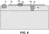
- the solar cell device comprises at least one of inconsistencies 14, 16a and 16b, at a surface of a semiconductor substrate 10 having a solar cell active region formed therein.
- a patterned insulating layer 70a, 70b is positioned over the one or more inconsistencies 16a and 16b.
- the insulating layer is formed only in discrete areas over and optionally surrounding the inconsistencies.
- the insulating layer 70 can be a permanent part of the solar cell device.
- the inconsistency 16b is a hole in the semiconductor substrate 10
- the patterned insulating layer 70b at least partially fills the hole.
- the patterned insulating layer 70a encapsulates the particle.
- the insulating layer 70 may be formed only on, or substantially only on, areas of the substrate over which a conductive line 24 will be formed and that have inconsistencies, such as between an inconsistency and a bus bar, contact region or a grid line.
- the term "substantially only on” as used here is defined to mean that the insulating layer extends out a lateral distance, D o , ( FIG. 7B ) from the metallization by an amount that is no greater than 50% of the width dimension, W m , of the metallization at the point at which the insulating layer is located.
- the conductive line 24 illustrated in FIG. 8 can comprise any metal or conductive material that is suitable for solar cell wiring, including any of the metals or other conductive materials described herein.
- the conductive line 24 may comprise an optional adhesion layer, as also described herein.
Landscapes
- Photovoltaic Devices (AREA)
- Electrodes Of Semiconductors (AREA)
- Internal Circuitry In Semiconductor Integrated Circuit Devices (AREA)
Abstract
Description
- The present disclosure is directed to methods of making wiring for solar cells on semiconductor substrates comprising inconsistencies, and to devices formed by the methods.
- Most solar cells include front wiring for collecting electrical current produced by the solar cell device. The front wiring is configured to have long, thin metal grid lines that terminate into bus bars. The bus bars collect large amounts of current from the grid lines and carries it to contact regions. Inconsistencies in the solar cell surface on which the wiring is formed can cause low cell performance that results from the metal wiring overlapping with inconsistencies in the semiconductor layers. For example, the inconsistencies can cause shorting and/or increase resistance of the wiring to undesirable levels.
FIG. 1 shows an example of asolar cell device 8 formed on asemiconductor substrate 10. As shown inFIG. 2 ,semiconductor substrate 10 includes asupport substrate 10a comprising germanium or silicon, a III/V singlecrystal device layer 10b (e.g., GaAs and/or InGaP) andfront wiring 12.Semiconductor substrate 10 can haveinconsistencies Inconsistency 14 is on thesemiconductor substrate 10, but does not contact thefront wiring 12 and thus would have little or no impact on performance.Inconsistency 16, however, is under a grid line and thus can potentially degrade solar cell performance. Inconsistencies that contact any part of thefront wiring 12 may potentially degrade performance, including inconsistencies positioned under thebus bars 18,contact regions 20 orgrid lines 22. -
FIG. 2 showsfront wiring 12 onsemiconductor substrate 10 havinginconsistencies inconsistency 16a is in the form of a particle, such as a particle that has fallen during the deposition of the solar cell material, leading to a tall, non-planar surface feature that may potentially increase the resistance of any wiring formed thereon. Anotherinconsistency 16b can occur as a no growth region that appears as a hole in the semiconductor substrate, which can potentially increase resistance and/or cause an electrical short between active regions of the device, thereby degrading device performance. - Various approaches are known for fabrication of the front metal wiring of solar cell devices. One common approach employs a lift-off technique to pattern metal lines. This process includes forming a patterned polymer lift-off mask on the semiconductor substrate. The lift-off mask is patterned for forming a desired solar cell wiring configuration using techniques well known in the art. The patterned lift-off mask has gaps exposing underlying portions of the substrate. A metal layer is blanket deposited from a directional process, such as evaporation, on the patterned lift-off mask and on exposed areas of the semiconductor substrate. The device is then soaked in solvents that "lift off" the patterned lift-off mask and overlying metal layers, while leaving metal not formed on the lift-off mask on the semiconductor substrate to form the wiring. In another conventional approach for fabricating front wiring, metal is selectively deposited by electrolysis (also referred to herein as electroplating), in areas of the substrate that are exposed through the patterned mask, but not on the patterned mask itself. The patterned mask can then be removed and the selectively deposited metal remains as the conductive wiring.
- Other known processes for forming front wiring include first blanket depositing a metal layer using any suitable process, such as by evaporation or electroplating, and then patterning the metal layer using well known photolithographic techniques. Such photolithographic techniques can include depositing and developing a photoresist layer to form a pattered photoresist on the metal layer. The metal layer can then be patterned by removing the areas of the metal not protected by the patterned photoresist using well known etching processes. Following etching, the patterned photoresist is then removed to leave the patterned metal wiring on the substrate.
- The processes described above for forming front wiring on solar cells include the formation of a photoresist pattern. As is well known in the art, forming such a photoresist pattern generally involves exposing the photoresist to radiation through a photomask. Such photomasks require much time and expense to fabricate, and are repeatedly used to form essentially the same photoresist patterns to mass produce many thousands or millions of the same solar cell devices. Because the photomasks are not easily modified, the photoresist pattern cannot be readily modified to fabricate different front wiring patterns for individual devices.
- A process that can allow for modification of front wiring on solar cells and other films based on the inconsistencies of a particular semiconductor substrate would be a valuable step forward in the art.
- The present disclosure is directed to a method of processing a solar cell device. The method comprises detecting at least one inconsistency at a surface of a semiconductor substrate having a solar cell active region formed therein. A deposition pattern is determined based on the location of the at least one inconsistency. A material is selectively deposited on the substrate according to the deposition pattern.
- The present disclosure is also directed to a solar cell device. The solar cell device comprises at least one inconsistency at a surface of a semiconductor substrate having a solar cell active region formed therein. A conductive line is configured to avoid the at least one inconsistency.
- The present disclosure is further directed to a solar cell device. The solar cell device comprises at least one inconsistency at a surface of a semiconductor substrate having a solar cell active region formed therein. A front wiring is on the surface of the semiconductor substrate for collecting electrical current produced by the solar cell device. The front wiring comprises a conductive line positioned over one or more of the at least one inconsistencies. The solar cell device further comprises a patterned insulating layer separating the conductive line from the one or more inconsistencies.
- It is to be understood that both the foregoing general description and the following detailed description are exemplary and explanatory only and are not restrictive of the present teachings, as claimed.
- The accompanying drawings, which are incorporated in and constitute a part of this specification, illustrate aspects of the present teachings and together with the description, serve to explain the principles of the present teachings.
-
FIG. 1 shows a top view of a conventional wiring scheme implemented on a solar cell device. -
FIG. 2 illustrates a cross-sectional view of an exemplary conventional solar cell device that includes wiring formed over inconsistencies. -
FIG. 3 shows an example process flow of a method of processing a solar cell device, according to the present disclosure -
FIG. 4 shows a top view of an example deposition pattern in which the initial wiring scheme has been modified so that a conductive line avoids a inconsistency, according to the present disclosure. -
FIG. 5A shows a cross-sectional view of one example of such a patterned mask that covers a inconsistency so that a subsequently deposited conductive line is deposited proximate to, but not in contact with, the inconsistency, according to the present disclosure. -
FIG. 5B shows a cross-sectional view of one example of such a patterned mask that covers a inconsistency so that a subsequently deposited conductive line is deposited proximate to, but not in contact with, the inconsistency, according to the present disclosure. -
FIGS. 6A, 6B and 6C illustrate an example of a method of patterning a metal layer using selective deposition of a mask, according to the present disclosure. -
FIGS. 7A and 7B illustrate a process for selectively depositing an insulating material on a inconsistency, according to the present disclosure. -
FIG. 8 illustrates a cross-sectional view of a solar cell device that comprises a patterned insulating layer positioned over inconsistencies, according to the present disclosure. -
FIG. 9 illustrates a schematic view of an apparatus comprising a print head for selective deposition that is integrated on the same scan head as an inspection device that is used for detecting inconsistencies, according to the present disclosure. - It should be noted that some details of the figures have been simplified and are drawn to facilitate understanding rather than to maintain strict structural accuracy, detail, and scale.
- Reference will now be made in detail to the present teachings, examples of which are illustrated in the accompanying drawings. In the drawings, like reference numerals have been used throughout to designate identical elements. In the following description, reference is made to the accompanying drawings that form a part thereof, and in which is shown by way of illustration specific examples of practicing the present teachings. The following description is, therefore, merely exemplary.
- As described above, solar cells are formed using semiconductor substrates that may include surface inconsistencies. The present disclosure is directed to a method of processing a solar cell device that can ameliorate certain problems associated with forming conductive wiring on the inconsistencies. Using the method, inconsistencies on the semiconductor device are located. The conductive wiring is then formed to avoid the inconsistencies. Alternatively to, or in addition to, forming the wiring to avoid the inconsistencies, insulating layers can be used to encapsulate and/or fill the inconsistencies prior to forming the wiring, thereby separating the wiring from the inconsistencies. The disclosed methods can allow for improved current gathering by the wiring on the solar cell, potentially improve device yield and/or provide for increased output power of the solar cell by modifying and/or tailoring the wiring on the solar cell device.
-
FIG. 3 shows an example process flow of the method. As indicated atprocess element 30 ofFIG. 3 , the method comprises detecting and determining the location of at least one inconsistency at a surface of a semiconductor substrate having a solar cell active region formed therein. The term "inconsistency" as used herein means any surface defect, non-planar surface feature or other surface irregularity that can cause shorting and/or increase resistance of thefront wiring 12 if thefront wiring 12 is formed thereon compared to the resistance of the wiring if the inconsistency were not present. Examples of such inconsistencies are discussed above with respect toFIG. 2 . Techniques and apparatuses for detecting and locating inconsistencies are well known in the art and are discussed in more detail below. A deposition pattern is determined based on the location of the inconsistency, as atprocess element 32. Selective deposition techniques can then be employed to selectively deposit a material on the substrate according to the determined deposition pattern, as atprocess element 34. - Referring to
FIGS. 4 and5 ,semiconductor substrate 10 can comprise any semiconductor material suitable for solar cell device fabrication. For example, the semiconductor substrate can include asupport substrate 10a comprising germanium single crystal or silicon single crystal. One or more III/V single crystal materials, such as GaAs and/or InGaP, is epitaxially grown on thesupport substrate 10a. The III/V material can include multiple layers, such as a III/V singlecrystal device layer 10b comprising, for example, InGaP, in which a top solar cell is formed; and a III/V singlecrystal cap layer 10c comprising, for example, GaAs, that can reduce contact resistance and surface recombination, as is well known in the art. Thesemiconductor substrate 10 can be doped with one or more n-type or p-type dopants to form at least one active region of the solar cell, which may comprise a p-n junction as is well known in the art. Exemplaryactive regions FIG. 5 , although any suitable type or number of active regions can be employed. - Referring to
FIG. 4 , thesemiconductor substrate 10 on which the wiring scheme is to be implemented is scanned forinconsistencies semiconductor substrate 10 can be scanned. If upon scanning the semiconductor substrate a inconsistency is found, the position of the inconsistency on thesemiconductor substrate 10 is determined. Detecting a inconsistency at a surface of the semiconductor substrate can be carried out using any suitable inconsistency detection system. Inconsistency detection systems are available for scanning and locating inconsistencies on semiconductor substrates. Examples of suitable detection systems include the ICOS WI-2280 Series, the Candela CSxx and CS9920 Series, the Surfscan Series all of which are made by KLA Tencor of Milpitas, California. Another example is the AWX™ Series made by Rudolph Technologies Inc., of Flanders, New Jersey. - Suitable detection systems can utilize reflected light, transmitted light, photoluminescence, electroluminescence or combinations thereof to detect inconsistencies. For photoluminescence, light emitted from the top cell of the solar cell device can potentially be used for detecting inconsistencies. For example, a GaAs cap layer can absorb the light used to excite the InGaP device layer and will absorb the photoluminescence exciting the material. The GaAs cap can be made relatively thin, such as, for example, about 5 nm to about 200 nm, to achieve photoluminescence inspection.
- Differential interference contrast microscopy, also known as Nomarski interference contrast or Nomarski microscopy can also be employed during inconsistency detection to increase contrast. Differential interference contrast microscopy employs an optical microscope with polarizers arranged to have increased sensitivity to height changes on a sample, which increases contract and visibility of inconsistencies, as is well known in the art.
- Referring to process
element 32 ofFIG. 3 , determining a deposition pattern based on the location of the inconsistency can optionally comprise providing an initial wiring scheme for the solar cell device. In general, the initial wiring scheme can comprise any desired pattern for forming the wiring of a solar cell device being manufactured. As an example, an initial wiring scheme could comprise the pattern for depositingfront wiring 12 on thesolar cell device 8, as shown inFIG. 1 . For purposes of the present disclosure, the initial wiring scheme can be provided in any suitable manner, such as a set of software instructions that are compatible for guiding a printing apparatus for purposes of selectively depositing materials to form the desired pattern forfront wiring 12 on thesolar cell device 8. One of ordinary skill in the art would readily be able to provide a suitable initial wiring scheme, given the present disclosure. - Using the known position of the inconsistency as determined during
process element 30, it can then be determined whether implementing a portion of the initial wiring scheme on thesemiconductor substrate 10 will result in aconductive line 24 that overlays the inconsistency, such as is the case withinconsistency 16 inFIG. 1 . In the event it is determined that implementing a portion of the initial wiring scheme will result in aconductive line 24 that overlays the inconsistency, a modification to the initial wiring scheme can then be made that avoids the inconsistency. As discussed herein, avoiding the inconsistency can reduce the risk of shorting and or avoid an undesirable increase in resistance of the front wiring, thereby potentially providing for improved current gathering by the wiring on the solar cell, improved device yield and/or increased output power of the solar cell. -
FIG. 4 shows an example deposition pattern in which the initial wiring scheme forfront wiring 12 ofFIG. 1 has been modified so thatconductive line 24 avoidsinconsistency 16. In this example, the modified wiring scheme comprises aconductive line 24 that circumvents the inconsistency so that theconductive line 24 is positioned proximate to, but not over, the inconsistency. The term "proximate to" in the context of positioning a conductive line to avoid a inconsistency is defined herein to be any distance that will cause the conductive line to avoid the inconsistency while not overlapping adjacent conductive lines. For example, the conductive line can be positioned so that at its closest point to the inconsistency, it is positioned at a distance of from 0.001 microns to 5 microns from the inconsistency, such as 0.01 microns to 2 microns. The modification can be made to any portion of the initial wiring scheme that may be positioned on a inconsistency, such asbus bar 18,contact region 20 or agrid line 22, all of which may be referred to herein as aconductive line 24. While the deposition pattern can be determined as described above, any other suitable technique for determining a deposition pattern that avoids the inconsistencies can be employed. - After determining the deposition pattern, any suitable selective deposition techniques can be used to deposit a material on the semiconductor substrate using the deposition pattern as a guide. The term "on" as used herein does not require direct physical contact and thus allows for intervening layers between the semiconductor substrate and the deposition pattern formed on the semiconductor substrate. Further, anytime the term "on" is employed herein to describe a relationship between layers, direct physical contact is contemplated as a possible option. The term "directly on" is defined to mean that direct physical contact is made.
- As one example of selectively depositing material, the conductive wiring itself is selectively deposited on the
semiconductor substrate 10 in the determined deposition pattern. Alternatively, a mask pattern can be selectively deposited and used to form the conductive lines in the desired deposition pattern. - In the case of selectively depositing the wiring, any suitable conventional or later developed method for selectively depositing conductive lines can be employed. For example, a conductive ink can be selectively deposited to form conductive lines using an inkjet print head, as is well known in the art. Still other techniques are known for selectively depositing various conductive materials, including micro- or nano-sized materials that may be dry, in a paste, suspended in a liquid, or are a liquid.
- The resulting conductive lines can comprise any suitable conductive material, such as one or more metals selected from aluminum, gold, silver, copper and nickel, which can be selectively deposited. The use of the term "comprise" here is meant to include both pure or substantially pure materials, such as the metals listed, or alloys of any of these materials (e.g., aluminum alloys, gold alloys, silver alloys or copper alloys), as well as multi-layer metal structures, that are suitable for front wiring of a solar cell. Examples of alloys of these metals that are suitable for solar cell wiring are well known in the art. These metals and their alloys provide for low resistance of the front wiring and/or good adhesion to the substrate, as is well known in the art. An example of a multi-layer structure for
conductive line 24 can comprise a relatively thin adhesion layer comprising a conductive material that adheres well to the substrate, such as a nickel or nickel alloy layer. The adhesion layer can be, for example, 0.01 micron to 1 micron in thickness. A thicker metal conductive material, such as aluminum, gold, silver, copper or alloys of any of these materials, can be deposited on the adhesion layer. The thicker metal layer forms the bulk of theconductive line 24 and can be, for example, 1 micron to 100 microns thick. Such adhesion layers provide improved adhesion of theconductive line 24 to thesemiconductor substrate 10. Multi-layerconductive lines 24 can also optionally include one or more additional layers, such as a diffusion barrier to prevent mixing of the metal that can potentially degrade the conductive line, a contact layer at the metal/semiconductor junction to provide low resistance contact between the conductive line and the semiconductor substrate and a capping layer on top of the conductive line to promote connections to external conductors by limiting oxidation and/or controlling roughness. Adhesion layers, diffusion layers, contact layers, and capping layers are generally well known in the art for use in conductive lines. In a specific example, theconductive line 24 can include a first layer comprising nickel at the semiconductor substrate/conductive line interface that is relatively thin (e.g., 0.01 micron to 1 micron, such as 0.1 micron) and that acts as a contact layer, diffusion barrier and adhesion layer, a conducting layer that can comprise, for example, aluminum, copper or silver that is relatively thick (e.g., 1 micron to 100 microns, such as 6 microns) on the nickel layer; and a capping layer on the conducting layer, the capping layer comprising, for example gold that can be relatively thin compared to the conducting layer (e.g., 0.01 microns to 1 micron, such as 0.1 micron). Any of the conductive lines described in this disclosure can comprise any of the conductive materials set forth in this paragraph, and may optionally include one or more layers selected from an adhesion layer, diffusion layer, contact layer and capping layer. - Referring to
FIG. 5A , another example of selectively depositing the material comprises selectively depositing a patternedmask 50 that is then used to form thefront wiring 12 in a desired pattern on thesemiconductor substrate 10. Any suitable type of selectively deposited mask can be employed as patternedmask 50. Techniques for selectively depositing such masks are well known in the art.Patterned mask 50 can comprise any suitable polymer materials, such as polyamides, polyimides, or photoresist.Patterned mask 50 can be deposited using a printing process, such as inkjet printing, that selectively deposits that mask material in a pattern on thesemiconductor substrate 10.FIG. 5 shows one example of a lift-off process employing a patternedmask 50 that covers one or more inconsistencies, such as theinconsistency 16, so that subsequently depositedconductive line 24 is deposited proximate to, but not in contact with, the inconsistency. Ametal layer 52 is then deposited over both the patternedmask 50 and on the areas of the underlying substrate not protected by the patternedmask 50. An optional adhesion layer (not shown) can be formed prior to formingmetal layer 52 onsemiconductor substrate 10, as described in detail above.Conductive line 24 is then formed by removing the patternedmask 50 along with the portions ofmetal layer 52 that are formed thereon from the semiconductor substrate. Portions of themetal layer 52 and, if deposited, the optional adhesion layer, that are not deposited on the patternedmask 50 remain as the patterned wiring, which includesconductive line 24. -
FIG. 5B illustrates an alternative process that is similar to the lift-off process described above, except thatmetal layer 52 is not deposited over the entire patternedmask 50, but instead is selectively deposited only on or around portions of thesemiconductor substrate 10 that are not protected by the patternedmask 50. In this process, the patternedmask 50 can be selectively deposited as described above in the lift-off process ofFIG. 5A , so that the mask covers one or more inconsistencies, such asinconsistency 16. After forming patternedmask 50, themetal layer 52 can be deposited using any suitable selective deposition technique, such as an electroplating process or by selectively printing metal inks using, for example, an inkjet type printer. Anoptional adhesion layer 53, as described above, is also shown, and may be deposited by any suitable selective deposition technique, which may be the same or different than the process used to selectively depositmetal layer 52. The electroplating process is potentially capable of forming themetal layer 52 and theoptional adhesion layer 53 only in areas of the substrate not protected by the patternedmask 50. The metal ink printing process, on the other hand, may depositmetal layer 52 and theoptional adhesion layer 53 in areas of the substrate not protected by patternedmask 50, and optionally on portions of the patternedmask 50 surrounding the areas that are not protected. The patternedmask 50 can then be removed, along with anymetal layer 52 and theoptional adhesion layer 53 that may have been formed thereon. Thus, the patterned mask can be used to control the dimension of a metal grid deposited by selective deposition processes such as electrolysis or a metal ink deposition process. After removing the patternedmask 50, a remaining portion ofmetal layer 52 andoptional adhesion layer 53 on thesemiconductor substrate 10 forms theconductive line 24. In this manner, theconductive line 24 can be routed around any inconsistencies on thesemiconductor substrate 10. As discussed above, avoiding the inconsistency can reduce the risk of shorting and/or avoid an undesirable increase in resistance of the wiring, thereby potentially providing for improved current gathering by the wiring on the solar cell, improved device yield and/or increased output power of the solar cell. - A process illustrated by
FIGS. 6A to 6C is yet another example of a method of patterning ametal layer 52 by selectively depositing a mask. As part of the process, aphotoresist layer 60 is blanket deposited over thesemiconductor substrate 10, as shown inFIG. 6A . Then a patternedradiation mask 62 is selectively deposited over thephotoresist layer 60. As described below, the patternedradiation mask 62 can be used to selectively expose portions of thephotoresist layer 60 to radiation, and thus can take the place of a conventional photomask in a photolithographic process. However, unlike a conventional photomask, the patternedradiation mask 62 can be varied for each device that is fabricated. Thus, the patternedradiation mask 62 can be selectively deposited in a unique deposition pattern that results in a wiring configuration that avoids theinconsistency 16, as shown inFIG. 6C . - In this method, and any of the other methods for depositing wiring patterns disclosed herein, the inconsistencies are only an issue if they are beyond the tolerances established by engineering, as would be understood by one of ordinary skill in the art. Thus, for example, the processes of the present disclosure can optionally include determining whether detected inconsistencies are within tolerance and thus not likely to cause wiring problems, or outside of tolerance and therefore a potential cause of shorting or increased resistance, as described herein. If it is determined that an inconsistency is within tolerance, there may be no reason to adjust the deposition pattern to avoid the inconsistency and the wiring pattern can be formed in contact with the inconsistency. If, on the other hand, the inconsistency is outside of established tolerances, the inconsistency can be avoided using any of the processes described herein.
- After selectively depositing the patterned
radiation mask 62, areas of thephotoresist layer 60 not protected by the patternedradiation mask 62 are then exposed to radiation, as illustrated by the arrows inFIG. 6A , to form a latent photoresist pattern 60a. Thephotoresist layer 60 is then developed using chemical processing to formphotoresist pattern 60b, as illustrated inFIG. 6B . Any suitable conventional or later developed techniques for depositing and developing the photoresist mask can be employed. - The portions of the
metal layer 52 not protected byphotoresist pattern 60b can then be etched using conventional or later developed etching techniques to provide a wiring configuration comprising theconductive line 24. As described herein,conductive line 24 can be patterned so as to be proximate to, but not in contact with, theinconsistency 16. In an alternative process, the selectively deposited patternedradiation mask 62 can be employed to pattern the patternedmask 50 used in the processes described herein with respect toFIGS. 5A and 5B . In the processes described herein with respect toFIGS. 6A, 6B and 6C , an optional adhesion layer can also be formed prior to formingmetal layer 52 onsemiconductor substrate 10, as described in detail above. - Referring back to
FIG. 6A , the patternedradiation mask 62 can comprise any material that can be selectively deposited and that can effectively block the radiation used to expose thephotoresist layer 60. For example, the patternedradiation mask 62 can comprise a black ink, or other colored ink, that can block the radiation used for exposing thephotoresist layer 60. - In another example, the process elements of determining a deposition pattern and selectively depositing the material, as referred to in
process elements 32 and 34 (FIG. 3 ) can respectively comprise determining a deposition pattern for an insulating material to be formed on theinconsistency 16 and then selectively depositing an insulatinglayer 70 on theinconsistency 16. Such an example is illustrated inFIGS. 7A, 7B and8 . By depositing the insulatinglayer 70 on theinconsistency 16, the inconsistency can be made suitable for forming wiring thereon without substantially degrading device performance. Any suitable insulating material that can be selectively deposited can be employed. As one example, the insulating layer can comprise at least one material chosen from an electrically insulating polymer and an oxide ceramic, which materials are capable of electrically insulating an inconsistency from the front wiring. Further, the insulatinglayer 70 can be deposited in any suitable manner. For example, aprint head 72, such as is used in inkjet technology, can be employed to selectively deposit the insulating material. The insulatinglayer 70 can be deposited to cover the entire inconsistency, thereby encapsulating theinconsistency 16 to prevent physical contact with the conductive line subsequently formed thereon. Alternatively, only a portion of theinconsistency 16 on which a subsequently deposited conductive line is to be formed may be covered by insulatinglayer 70. Employing the insulatinglayer 70 as described here is another method for avoiding contact of the front wiring with the inconsistency, which can reduce the risk of shorting and/or avoid an undesirable increase in resistance of the wiring, thereby potentially providing for improved current gathering by the wiring on the solar cell, improved device yield and/or increased output power of the solar cell. - After insulating
layer 70 is deposited to encapsulate the inconsistency, any of the processes described above for forming theconductive line 24 can optionally be carried out. Theconductive line 24 can be routed around the inconsistency, such as in the processes described above with respect toFIGS. 5A or 5B , which may further reduce the risk that the any non-planar surface topography caused by the inconsistency will increase the resistance of the front wiring compared to the resistance if the inconsistency were not present. - Alternatively, the insulating
layer 70 can be deposited either before or after a patterned photoresist mask 51 (shown inFIG. 7A ) is formed as part of a lift-off process for forming aconductive line 24. The patternedphotoresist mask 51 can be formed in a desired pattern using a conventional photomask to expose the photoresist layer, so that theinconsistency 16 is not covered by the patternedphotoresist mask 51, as shown inFIG. 7A . Ametal layer 52 is then blanket deposited, as described above inFIG. 5A , followed by removal of the photoresist and the portion ofmetal layer 52 formed thereon to formconductive line 24, as shown inFIG. 7B . In this lift-off process, even though the metal layer is formed over the inconsistency, the insulatinglayer 70 can reduce or prevent undesired effect on the device that may otherwise be caused by forming theconductive line 24 directly on theinconsistency 16. In the processes described in connection withFIGS. 7A, 7B and8 , an optional adhesion layer can be formed as part of formingconductive line 24, as described in detail above. - The processes described herein can be carried out using an apparatus for detecting the inconsistencies and a separate apparatus for selectively depositing material. Such a process can include scanning the semiconductor substrate to locate inconsistencies. Then after the entire scanning process of the semiconductor substrate is complete, a separate apparatus is employed to selectively deposit material based on the location of the inconsistencies.
- Alternatively, a single apparatus can be used for both detecting inconsistencies and selective deposition. An example of such an apparatus is illustrated in
FIG. 9 , which shows aprint head 72 for selective deposition that is integrated on thesame scan head 90 as aninspection device 92 that is used for detecting inconsistencies. There can be advantages of using the same apparatus for both detecting the inconsistency and selectively depositing the material on thesemiconductor substrate 10. For instance, the integrated arrangement shown inFIG. 9 can potentially improve the precision and/or accuracy of theprint head 72 for depositing material so as to avoid or encapsulate inconsistencies, which can potentially have sizes on the order of microns or even nanometers. - This disclosure is also directed to a solar cell device, examples of which are illustrated in
FIGS. 4 and6C . The solar cell device comprises at least one inconsistency at a surface of asemiconductor substrate 10 having a solar cell active region formed therein. Theinconsistency 16 can be any type of inconsistency, including any of the inconsistencies described herein. Aconductive line 24 is configured to avoid the inconsistency. The phrases "configured to avoid the inconsistency" or "configured to avoid the at least one inconsistency" are defined herein to mean that the path of theconductive line 24 deviates from either a linear path of the conductive line or from an overall regular pattern of the metallization that would cause the conductive line to come into contact with an inconsistency in order to avoid the inconsistency. As shown in the conventional example ofFIG. 1 , thefront wiring 12 of asolar cell device 8 is generally formed in a regular pattern that may include, for example, regularly spacedgrid lines 22, although other regular patterns with linear or non-linear grid lines could also be employed. Referring toFIG. 4 , in one example of the devices of the present disclosure, the conductive line (e.g., grid line or bus bar) comprises amajor portion 24a that is substantially linear (e.g., it has a linear, longitudinal axis that extends for 50% or more if its length). Theconductive line 24 further comprises aminor portion 24b where, if the conductive line were to remain substantially linear (e.g., continue to follow the major longitudinal axis), would cause theminor portion 24b of theconductive line 24 to intersect theinconsistency 16. Theminor portion 24b deviates from the substantially linear path of themajor portion 24a (e.g., the conductive line deviates so that it is no longer positioned along the longitudinal axis ofmajor portion 24a) so as to avoid theinconsistency 16. This allows the minor portion of the conductive line to be positioned proximate to, but not over, the inconsistency, as shown, for example, inFIG. 4 . Theconductive line 24 can comprise any metal or conductive material that is suitable for solar cell wiring, including any of the metals or other conductive materials described herein. Theconductive line 24 may comprise an optional adhesion layer, as also described herein. - This disclosure is also directed to a solar cell device as shown, for example, in
FIG. 8 . The solar cell device comprises at least one ofinconsistencies semiconductor substrate 10 having a solar cell active region formed therein. A patterned insulatinglayer more inconsistencies layer 70 can be a permanent part of the solar cell device. In one example where theinconsistency 16b is a hole in thesemiconductor substrate 10, the patterned insulatinglayer 70b at least partially fills the hole. In another example where theinconsistency 16a is a particle, the patterned insulatinglayer 70a encapsulates the particle. In another example, the insulatinglayer 70 may be formed only on, or substantially only on, areas of the substrate over which aconductive line 24 will be formed and that have inconsistencies, such as between an inconsistency and a bus bar, contact region or a grid line. The term "substantially only on" as used here is defined to mean that the insulating layer extends out a lateral distance, Do, (FIG. 7B ) from the metallization by an amount that is no greater than 50% of the width dimension, Wm, of the metallization at the point at which the insulating layer is located. Theconductive line 24 illustrated inFIG. 8 can comprise any metal or conductive material that is suitable for solar cell wiring, including any of the metals or other conductive materials described herein. Theconductive line 24 may comprise an optional adhesion layer, as also described herein. - Further, the disclosure comprises examples according to the following clauses:
- Clause 1. A method of processing a solar cell device, the method comprising:
detecting at least one inconsistency at a surface of a semiconductor substrate having a solar cell active region formed therein; determining a deposition pattern based on a location of the at least one inconsistency; and selectively depositing a material on the substrate according to the deposition pattern. - Clause 2. The method of Clause 1, wherein determining a deposition pattern based on the location of the at least one inconsistency comprises: providing an initial wiring scheme for the solar cell device; determining that implementing a first portion of the initial wiring scheme will result in a conductive line that overlays the inconsistency; and determining a modified wiring scheme that avoids the at least one inconsistency.
- Clause 3. The method of Clause 1, wherein selectively depositing the material comprises selectively depositing a conductive line configured to avoid the at least one inconsistency, the conductive line forming a portion of a front wiring on the solar cell device.
- Clause 4. The method of Clause 1, wherein the conductive line comprises one or more metals selected from aluminum, gold, silver, copper and nickel.
- Clause 5. The method of Clause 1, wherein selectively depositing the material comprises selectively depositing a patterned mask.
- Clause 6. The method of Clause 3, further comprising depositing a conductive line on areas of the substrate not protected by the patterned mask, the conductive line being selectively deposited by electroplating.
- Clause 7. The method of Clause 3, further comprising depositing a conductive line on areas of the substrate not protected by the patterned mask, the conductive line being selectively deposited by a metal ink deposition process, wherein the patterned mask controls a dimension of the conductive line.
-
Clause 8. The method of Clause 3, wherein the patterned mask covers the at least one inconsistency. - Clause 9. The method of Clause 6, further comprising depositing a metal layer over the patterned mask and then removing the patterned mask from the semiconductor substrate to pattern the metal layer.
-
Clause 10. The method of Clause 1, further comprising depositing a photoresist layer over the semiconductor substrate, wherein selectively depositing the material comprises selectively depositing a patterned radiation mask over the photoresist layer. - Clause 11. The method of Clause 0, further comprising exposing the photoresist layer and the patterned radiation mask to radiation and developing the photoresist layer to form a photoresist pattern.
-
Clause 12. The method of Clause 1, wherein selectively depositing the material comprises selectively depositing an insulating layer over the at least one inconsistency. - Clause 13. The method of
Clause 8, wherein the insulating layer comprises at least one material chosen from an electrically insulating polymer and an oxide ceramic. -
Clause 14. The method of Clause 1, wherein both detecting the at least one inconsistency and selectively depositing the material on the substrate are carried out using a single apparatus. - Clause 15. A solar cell device, comprising: at least one inconsistency at a surface of a semiconductor substrate having a solar cell active region formed therein; and a conductive line configured to avoid the at least one inconsistency.
-
Clause 16. The solar cell device ofClause 10, wherein the conductive line comprises a major portion that is substantially linear and a minor portion that deviates from being substantially linear so as to avoid the at least one inconsistency. - Clause 17. A solar cell device, comprising: at least one inconsistency at a surface of a semiconductor substrate having a solar cell active region formed therein; a front wiring on the surface of the semiconductor substrate for collecting electrical current produced by the solar cell device, the front wiring comprising a conductive line positioned over one or more of the at least one inconsistencies; and a patterned insulating layer separating the conductive line from the one or more inconsistencies.
-
Clause 18. The solar cell device of Clause 11, wherein the insulating layer is formed only in discrete areas over and optionally surrounding the one or more inconsistencies. - Clause 19. The solar cell device of Clause 11, wherein the one or more inconsistencies comprise a hole in the semiconductor substrate and the patterned insulating layer at least partially fills the hole.
-
Clause 20. The solar cell device of Clause 11, wherein the one or more inconsistencies comprise a particle. - Notwithstanding that the numerical ranges and parameters setting forth the broad scope of the disclosure are approximations, the numerical values set forth in the specific examples are reported as precisely as possible. Any numerical value, however, inherently contains certain errors necessarily resulting from the standard deviation found in their respective testing measurements. Moreover, all ranges disclosed herein are to be understood to encompass any and all sub-ranges subsumed therein.
- While the present teachings have been illustrated with respect to one or more implementations, alterations and/or modifications can be made to the illustrated examples without departing from the spirit and scope of the appended claims. In addition, while a particular feature of the present teachings may have been disclosed with respect to only one of several implementations, such feature may be combined with one or more other features of the other implementations as may be desired and advantageous for any given or particular function. Furthermore, to the extent that the terms "including," "includes," "having," "has," "with," or variants thereof are used in either the detailed description and the claims, such terms are intended to be inclusive in a manner similar to the term "comprising." Further, in the discussion and claims herein, the term "about" indicates that the value listed may be somewhat altered, as long as the alteration does not result in nonconformance of the process or structure to the intended purpose described herein. Finally, "exemplary" indicates the description is used as an example, rather than implying that it is an ideal.
- It will be appreciated that variants of the above-disclosed and other features and functions, or alternatives thereof, may be combined into many other different systems or applications. Various presently unforeseen or unanticipated alternatives, modifications, variations, or improvements therein may be subsequently made by those skilled in the art which are also intended to be encompasses by the following claims.
Claims (15)
- A method of processing a solar cell device (8), the method comprising:detecting (30) at least one inconsistency (14, 16) at a surface of a semiconductor substrate (10) having a solar cell active region formed therein;determining (32) a deposition pattern based on a location of the at least one inconsistency (14, 16); andselectively depositing a material on the substrate according to the deposition pattern, wherein selectively depositing the material comprises selectively depositing an insulating layer over the at least one inconsistency.
- The method of claim 1, wherein the insulating layer comprises at least one material chosen from an electrically insulating polymer and an oxide ceram ic.
- The method of claim 1, wherein both detecting the at least one inconsistency and selectively depositing the material on the substrate are carried out using a single apparatus.
- The method of claim 1, wherein determining a deposition pattern based on the location of the at least one inconsistency comprises:providing an initial wiring scheme for the solar cell device (8);determining that implementing a first portion of the initial wiring scheme will result in a conductive line (24) that overlays the inconsistency (16); anddetermining a modified wiring scheme that avoids the at least one inconsistency (16).
- The method of claim 1, wherein selectively depositing the material further comprises selectively depositing a conductive line configured to avoid the at least one inconsistency, the conductive line forming a portion of a front wiring on the solar cell device.
- The method of any of claims 4 or 5, wherein the conductive line comprises one or more metals selected from aluminum, gold, silver, copper and nickel.
- The method of any one of claims 4-6, wherein selectively depositing the material further comprises selectively depositing a patterned mask (50).
- The method of claim 7, further comprising depositing a conductive line (24) on areas of the substrate (10) not protected by the patterned mask (50), the conductive line being selectively deposited by electroplating.
- The method of claim 7 or 8, further comprising depositing a conductive line (24) on areas of the substrate (10) not protected by the patterned mask (50), the conductive line (24) being selectively deposited by a metal ink deposition process, wherein the patterned mask controls a dimension of the conductive line.
- The method of any one of claims 7-9, wherein the patterned mask (50) covers the at least one inconsistency (14, 16), the method
further comprising preferably depositing a metal layer (52) over the patterned mask (50) and then removing the patterned mask from the semiconductor substrate (10) to pattern the metal layer. - The method of any one of claims 1-10, further comprising depositing a photoresist layer (60) over the semiconductor substrate (10), wherein selectively depositing the material further comprises selectively depositing a patterned radiation mask (62) over the photoresist layer.
- The method of claim 11, further comprising exposing the photoresist layer (60) and the patterned radiation mask (62) to radiation and developing the photoresist layer (60) to form a photoresist pattern (60a, 60b).
- A solar cell device (8), comprising:at least one inconsistency (14, 16) at a surface of a semiconductor substrate (10) having a solar cell active region formed therein;a front wiring (12) on the surface of the semiconductor substrate for collecting electrical current produced by the solar cell device, the front wiring comprising a conductive line (24) positioned over one or more of the at least one inconsistencies (14, 16); anda patterned insulating layer (70) separating the conductive line from the one or more inconsistencies.
- The solar cell device of claim 12, wherein the insulating layer (70) is formed only in discrete areas over and optionally surrounding the one or more inconsistencies (14, 16).
- The solar cell device of claim 12, wherein the one or more inconsistencies (14, 16) comprise a hole in the semiconductor substrate (10) and the patterned insulating layer (70) at least partially fills the hole, or alternatively wherein the one or more inconsistencies (14, 16) comprise a particle.
Applications Claiming Priority (2)
| Application Number | Priority Date | Filing Date | Title |
|---|---|---|---|
| US15/475,757 US11233162B2 (en) | 2017-03-31 | 2017-03-31 | Method of processing inconsistencies in solar cell devices and devices formed thereby |
| EP18164625.8A EP3382892B1 (en) | 2017-03-31 | 2018-03-28 | Method of processing inconsistencies in solar cell devices and devices formed thereby |
Related Parent Applications (1)
| Application Number | Title | Priority Date | Filing Date |
|---|---|---|---|
| EP18164625.8A Division EP3382892B1 (en) | 2017-03-31 | 2018-03-28 | Method of processing inconsistencies in solar cell devices and devices formed thereby |
Publications (1)
| Publication Number | Publication Date |
|---|---|
| EP4071834A1 true EP4071834A1 (en) | 2022-10-12 |
Family
ID=61832417
Family Applications (2)
| Application Number | Title | Priority Date | Filing Date |
|---|---|---|---|
| EP18164625.8A Active EP3382892B1 (en) | 2017-03-31 | 2018-03-28 | Method of processing inconsistencies in solar cell devices and devices formed thereby |
| EP22175903.8A Pending EP4071834A1 (en) | 2017-03-31 | 2018-03-28 | Method of processing inconsistencies in solar cell devices and devices formed thereby |
Family Applications Before (1)
| Application Number | Title | Priority Date | Filing Date |
|---|---|---|---|
| EP18164625.8A Active EP3382892B1 (en) | 2017-03-31 | 2018-03-28 | Method of processing inconsistencies in solar cell devices and devices formed thereby |
Country Status (5)
| Country | Link |
|---|---|
| US (3) | US11233162B2 (en) |
| EP (2) | EP3382892B1 (en) |
| JP (1) | JP7329905B2 (en) |
| CN (1) | CN108695407B (en) |
| RU (1) | RU2762129C2 (en) |
Citations (4)
| Publication number | Priority date | Publication date | Assignee | Title |
|---|---|---|---|---|
| DE69227049T2 (en) * | 1991-02-20 | 1999-04-29 | Canon K.K., Tokio/Tokyo | Manufacturing method of a defect-free photoelectric conversion device |
| US20100210040A1 (en) * | 2008-11-17 | 2010-08-19 | Solopower, Inc. | Method and apparatus for reducing the effect of shunting defects on thin film solar cell performance |
| WO2013051433A1 (en) * | 2011-10-07 | 2013-04-11 | シャープ株式会社 | Defect repair method and defect repair device for photovoltaic element |
| US20140345683A1 (en) * | 2013-05-24 | 2014-11-27 | The Boeing Company | Shunt treatment in inverted and wafer bonded solar cells |
Family Cites Families (20)
| Publication number | Priority date | Publication date | Assignee | Title |
|---|---|---|---|---|
| JPH06151908A (en) * | 1992-11-05 | 1994-05-31 | Canon Inc | Defect sealing method for solar cell |
| NL1010635C2 (en) | 1998-11-23 | 2000-05-24 | Stichting Energie | A method of manufacturing a metallization pattern on a photovoltaic cell. |
| DE102004050269A1 (en) * | 2004-10-14 | 2006-04-20 | Institut Für Solarenergieforschung Gmbh | Process for the contact separation of electrically conductive layers on back-contacted solar cells and solar cell |
| EP1763086A1 (en) | 2005-09-09 | 2007-03-14 | Interuniversitair Micro-Elektronica Centrum | Photovoltaic cell with thick silicon oxide and silicon nitride passivation and fabrication method |
| US7375378B2 (en) | 2005-05-12 | 2008-05-20 | General Electric Company | Surface passivated photovoltaic devices |
| ITBG20060053A1 (en) * | 2006-10-13 | 2008-04-14 | Abb Service Srl | LOW VOLTAGE DEVICE WITH MOBILE CREW WITH HIGH ELECTRODYNAMIC SEALING |
| JP5543786B2 (en) | 2008-01-09 | 2014-07-09 | ローム株式会社 | Semiconductor device and manufacturing method thereof |
| WO2009094578A2 (en) | 2008-01-24 | 2009-07-30 | Applied Materials, Inc. | Improved hit solar cell structure |
| US7989729B1 (en) | 2008-03-11 | 2011-08-02 | Kla-Tencor Corporation | Detecting and repairing defects of photovoltaic devices |
| US8318239B2 (en) * | 2008-11-17 | 2012-11-27 | Solopower, Inc. | Method and apparatus for detecting and passivating defects in thin film solar cells |
| US8283558B2 (en) | 2009-03-27 | 2012-10-09 | The Boeing Company | Solar cell assembly with combined handle substrate and bypass diode and method |
| WO2011017740A1 (en) * | 2009-08-11 | 2011-02-17 | Newsouth Innovations Pty Limited | A method for the selective delivery of material to a substrate |
| NO20100616A1 (en) | 2010-04-28 | 2011-10-31 | Innotech Solar Asa | Method and apparatus for removing a defect from a solar cell |
| US8932724B2 (en) | 2010-06-07 | 2015-01-13 | General Atomics | Reflective coating, pigment, colored composition, and process of producing a reflective pigment |
| KR101292061B1 (en) | 2010-12-21 | 2013-08-01 | 엘지전자 주식회사 | Thin film solar cell |
| TWI559563B (en) | 2011-12-21 | 2016-11-21 | 太陽電子公司 | Hybrid polycrystalline germanium heterojunction back contact battery |
| US20130186461A1 (en) * | 2012-01-20 | 2013-07-25 | Dong-jin Kim | Solar cell and method of manufacturing the same |
| JP2015050295A (en) | 2013-08-30 | 2015-03-16 | 大日本印刷株式会社 | Method for manufacturing current collector sheet for solar cell module |
| JP6404474B2 (en) | 2015-06-30 | 2018-10-10 | 株式会社カネカ | Solar cell and solar cell module |
| JP6819996B2 (en) | 2016-10-14 | 2021-01-27 | 国立大学法人金沢大学 | Traffic signal recognition method and traffic signal recognition device |
-
2017
- 2017-03-31 US US15/475,757 patent/US11233162B2/en active Active
-
2018
- 2018-03-26 RU RU2018110629A patent/RU2762129C2/en active
- 2018-03-28 EP EP18164625.8A patent/EP3382892B1/en active Active
- 2018-03-28 EP EP22175903.8A patent/EP4071834A1/en active Pending
- 2018-03-29 JP JP2018063680A patent/JP7329905B2/en active Active
- 2018-03-30 CN CN201810274891.8A patent/CN108695407B/en active Active
-
2022
- 2022-01-12 US US17/647,839 patent/US11742442B2/en active Active
-
2023
- 2023-07-03 US US18/346,477 patent/US12119418B2/en active Active
Patent Citations (4)
| Publication number | Priority date | Publication date | Assignee | Title |
|---|---|---|---|---|
| DE69227049T2 (en) * | 1991-02-20 | 1999-04-29 | Canon K.K., Tokio/Tokyo | Manufacturing method of a defect-free photoelectric conversion device |
| US20100210040A1 (en) * | 2008-11-17 | 2010-08-19 | Solopower, Inc. | Method and apparatus for reducing the effect of shunting defects on thin film solar cell performance |
| WO2013051433A1 (en) * | 2011-10-07 | 2013-04-11 | シャープ株式会社 | Defect repair method and defect repair device for photovoltaic element |
| US20140345683A1 (en) * | 2013-05-24 | 2014-11-27 | The Boeing Company | Shunt treatment in inverted and wafer bonded solar cells |
Also Published As
| Publication number | Publication date |
|---|---|
| US20230352605A1 (en) | 2023-11-02 |
| EP3382892B1 (en) | 2022-06-15 |
| JP2018198307A (en) | 2018-12-13 |
| US20220140159A1 (en) | 2022-05-05 |
| CN108695407A (en) | 2018-10-23 |
| EP3382892A2 (en) | 2018-10-03 |
| RU2018110629A3 (en) | 2021-07-05 |
| US11233162B2 (en) | 2022-01-25 |
| EP3382892A3 (en) | 2018-12-26 |
| JP7329905B2 (en) | 2023-08-21 |
| RU2018110629A (en) | 2019-09-26 |
| CN108695407B (en) | 2023-04-25 |
| RU2762129C2 (en) | 2021-12-15 |
| US11742442B2 (en) | 2023-08-29 |
| US12119418B2 (en) | 2024-10-15 |
| US20180286992A1 (en) | 2018-10-04 |
Similar Documents
| Publication | Publication Date | Title |
|---|---|---|
| EP2610910B1 (en) | Light emitting diode array and printing head | |
| Bezshlyakh et al. | Directly addressable GaN-based nano-LED arrays: fabrication and electro-optical characterization | |
| JP6370305B2 (en) | Manufacturing method of adjacent region including LED wire and apparatus obtained by the manufacturing method | |
| TWI529953B (en) | Microwire metallization of photovoltaic devices with partially stripped optical coatings | |
| EP0228881A2 (en) | Tank overfill valve | |
| US10331057B2 (en) | Light emitting element device including light emitting thyristor and optical print head including the light emitting element device | |
| US8207443B2 (en) | Point contacts for polysilicon emitter solar cell | |
| JPH0832110A (en) | Edge emitting LED, method for manufacturing edge emitting light emitting element, method for measuring emission characteristics of edge emitting light emitting element | |
| US6617191B1 (en) | Method for anodizing silicon substrates for surface type acceleration sensors | |
| US6455836B1 (en) | Metallic optical barrier for photo-detector array is also interconnecting electrode | |
| US12119418B2 (en) | Method of processing inconsistencies in solar cell devices and devices formed thereby | |
| JPS63108709A (en) | Semiconductor device and manufacture of the same | |
| WO2019130859A1 (en) | Method for producing photoelectric conversion element, tool for plating, and plating apparatus | |
| Lange et al. | Contact and Bulk Resistivity Screening for Advanced Crystalline Silicon Solar Cell Concepts by an Economical and Reliable Transfer Length Measurement Method Based on Laser Micro‐Patterning | |
| JPH10284760A (en) | Manufacturing method of light receiving and emitting diode array chip | |
| TW506020B (en) | Hetero-bipolar transistor with T-formed emitter-terminal-contact and its production | |
| US10141235B2 (en) | Semiconductor device and method for manufacturing the same | |
| US20060208265A1 (en) | Light emitting diode and light emitting diode array | |
| JP2008112883A (en) | Light emitting diode array and method for manufacturing light emitting diode array | |
| Islam | Axial pin Junction Single GaAs Nanowire Solar Cell | |
| JP2003188411A (en) | Light emitting semiconductor device and manufacturing method thereof | |
| JP3439950B2 (en) | Semiconductor light emitting device | |
| KR100296710B1 (en) | Method of manufacturing a diamond vacuum microelectronic device | |
| JPH08298339A (en) | Manufacture of light emitting and receiving element | |
| US20100006146A1 (en) | Wafer-Specific Line Patterning For Solar Cells And The Like |
Legal Events
| Date | Code | Title | Description |
|---|---|---|---|
| PUAI | Public reference made under article 153(3) epc to a published international application that has entered the european phase |
Free format text: ORIGINAL CODE: 0009012 |
|
| STAA | Information on the status of an ep patent application or granted ep patent |
Free format text: STATUS: THE APPLICATION HAS BEEN PUBLISHED |
|
| AC | Divisional application: reference to earlier application |
Ref document number: 3382892 Country of ref document: EP Kind code of ref document: P |
|
| AK | Designated contracting states |
Kind code of ref document: A1 Designated state(s): AL AT BE BG CH CY CZ DE DK EE ES FI FR GB GR HR HU IE IS IT LI LT LU LV MC MK MT NL NO PL PT RO RS SE SI SK SM TR |
|
| RAP3 | Party data changed (applicant data changed or rights of an application transferred) |
Owner name: THE BOEING COMPANY |
|
| STAA | Information on the status of an ep patent application or granted ep patent |
Free format text: STATUS: REQUEST FOR EXAMINATION WAS MADE |
|
| 17P | Request for examination filed |
Effective date: 20230327 |
|
| RBV | Designated contracting states (corrected) |
Designated state(s): AL AT BE BG CH CY CZ DE DK EE ES FI FR GB GR HR HU IE IS IT LI LT LU LV MC MK MT NL NO PL PT RO RS SE SI SK SM TR |
|
| STAA | Information on the status of an ep patent application or granted ep patent |
Free format text: STATUS: EXAMINATION IS IN PROGRESS |
|
| 17Q | First examination report despatched |
Effective date: 20240925 |