EP4071552A1 - Molybdenum-carbide-containing pellicle for extreme ultraviolet lithography - Google Patents
Molybdenum-carbide-containing pellicle for extreme ultraviolet lithography Download PDFInfo
- Publication number
- EP4071552A1 EP4071552A1 EP22162246.7A EP22162246A EP4071552A1 EP 4071552 A1 EP4071552 A1 EP 4071552A1 EP 22162246 A EP22162246 A EP 22162246A EP 4071552 A1 EP4071552 A1 EP 4071552A1
- Authority
- EP
- European Patent Office
- Prior art keywords
- layer
- pellicle
- molybdenum carbide
- thickness
- extreme ultraviolet
- Prior art date
- Legal status (The legal status is an assumption and is not a legal conclusion. Google has not performed a legal analysis and makes no representation as to the accuracy of the status listed.)
- Pending
Links
- 229910039444 MoC Inorganic materials 0.000 title claims abstract description 104
- QIJNJJZPYXGIQM-UHFFFAOYSA-N 1lambda4,2lambda4-dimolybdacyclopropa-1,2,3-triene Chemical compound [Mo]=C=[Mo] QIJNJJZPYXGIQM-UHFFFAOYSA-N 0.000 title claims abstract description 103
- 238000001900 extreme ultraviolet lithography Methods 0.000 title claims abstract description 58
- 239000010410 layer Substances 0.000 claims abstract description 321
- 239000012792 core layer Substances 0.000 claims abstract description 124
- 239000000758 substrate Substances 0.000 claims abstract description 48
- 239000000463 material Substances 0.000 claims description 46
- 229910003178 Mo2C Inorganic materials 0.000 claims description 33
- 229910004205 SiNX Inorganic materials 0.000 claims description 13
- 150000004767 nitrides Chemical class 0.000 claims description 12
- 229910021332 silicide Inorganic materials 0.000 claims description 11
- FVBUAEGBCNSCDD-UHFFFAOYSA-N silicide(4-) Chemical compound [Si-4] FVBUAEGBCNSCDD-UHFFFAOYSA-N 0.000 claims description 11
- 229910010271 silicon carbide Inorganic materials 0.000 claims description 10
- 229910052726 zirconium Inorganic materials 0.000 claims description 10
- VYPSYNLAJGMNEJ-UHFFFAOYSA-N Silicium dioxide Chemical compound O=[Si]=O VYPSYNLAJGMNEJ-UHFFFAOYSA-N 0.000 claims description 9
- 229910052799 carbon Inorganic materials 0.000 claims description 9
- 229910020968 MoSi2 Inorganic materials 0.000 claims description 7
- 239000000203 mixture Substances 0.000 claims description 7
- 229910003465 moissanite Inorganic materials 0.000 claims description 6
- 229910052681 coesite Inorganic materials 0.000 claims description 4
- 229910052906 cristobalite Inorganic materials 0.000 claims description 4
- 239000000377 silicon dioxide Substances 0.000 claims description 4
- 229910052682 stishovite Inorganic materials 0.000 claims description 4
- 229910052905 tridymite Inorganic materials 0.000 claims description 4
- 238000002834 transmittance Methods 0.000 description 88
- 238000000034 method Methods 0.000 description 27
- OKTJSMMVPCPJKN-UHFFFAOYSA-N Carbon Chemical compound [C] OKTJSMMVPCPJKN-UHFFFAOYSA-N 0.000 description 19
- 238000004544 sputter deposition Methods 0.000 description 19
- 229910021389 graphene Inorganic materials 0.000 description 12
- 239000000126 substance Substances 0.000 description 12
- 238000004519 manufacturing process Methods 0.000 description 10
- 239000010409 thin film Substances 0.000 description 10
- 229910052750 molybdenum Inorganic materials 0.000 description 9
- HBMJWWWQQXIZIP-UHFFFAOYSA-N silicon carbide Chemical compound [Si+]#[C-] HBMJWWWQQXIZIP-UHFFFAOYSA-N 0.000 description 9
- 238000000231 atomic layer deposition Methods 0.000 description 8
- 238000005229 chemical vapour deposition Methods 0.000 description 8
- 238000000151 deposition Methods 0.000 description 8
- 238000001459 lithography Methods 0.000 description 8
- 239000004065 semiconductor Substances 0.000 description 8
- 239000001257 hydrogen Substances 0.000 description 7
- 229910052739 hydrogen Inorganic materials 0.000 description 7
- 229910052580 B4C Inorganic materials 0.000 description 6
- 239000004215 Carbon black (E152) Substances 0.000 description 5
- 238000005516 engineering process Methods 0.000 description 5
- 238000010438 heat treatment Methods 0.000 description 5
- 229930195733 hydrocarbon Natural products 0.000 description 5
- 150000002430 hydrocarbons Chemical class 0.000 description 5
- 238000001039 wet etching Methods 0.000 description 5
- ZOKXTWBITQBERF-UHFFFAOYSA-N Molybdenum Chemical compound [Mo] ZOKXTWBITQBERF-UHFFFAOYSA-N 0.000 description 4
- 229910003481 amorphous carbon Inorganic materials 0.000 description 4
- 239000000356 contaminant Substances 0.000 description 4
- 230000003628 erosive effect Effects 0.000 description 4
- 229910052751 metal Inorganic materials 0.000 description 4
- 239000002184 metal Substances 0.000 description 4
- 239000011733 molybdenum Substances 0.000 description 4
- UFHFLCQGNIYNRP-UHFFFAOYSA-N Hydrogen Chemical compound [H][H] UFHFLCQGNIYNRP-UHFFFAOYSA-N 0.000 description 3
- 230000008021 deposition Effects 0.000 description 3
- 239000007789 gas Substances 0.000 description 3
- 229910052710 silicon Inorganic materials 0.000 description 3
- 229910021354 zirconium(IV) silicide Inorganic materials 0.000 description 3
- 229910052581 Si3N4 Inorganic materials 0.000 description 2
- XUIMIQQOPSSXEZ-UHFFFAOYSA-N Silicon Chemical compound [Si] XUIMIQQOPSSXEZ-UHFFFAOYSA-N 0.000 description 2
- 229910021393 carbon nanotube Inorganic materials 0.000 description 2
- 239000002041 carbon nanotube Substances 0.000 description 2
- 239000003054 catalyst Substances 0.000 description 2
- 238000011109 contamination Methods 0.000 description 2
- 230000007547 defect Effects 0.000 description 2
- 230000002950 deficient Effects 0.000 description 2
- 238000001312 dry etching Methods 0.000 description 2
- 239000011261 inert gas Substances 0.000 description 2
- 230000010354 integration Effects 0.000 description 2
- 239000011229 interlayer Substances 0.000 description 2
- 239000012528 membrane Substances 0.000 description 2
- 150000001247 metal acetylides Chemical class 0.000 description 2
- 238000005459 micromachining Methods 0.000 description 2
- 239000010703 silicon Substances 0.000 description 2
- 229910052814 silicon oxide Inorganic materials 0.000 description 2
- 229910052719 titanium Inorganic materials 0.000 description 2
- 238000012546 transfer Methods 0.000 description 2
- ZOXJGFHDIHLPTG-UHFFFAOYSA-N Boron Chemical compound [B] ZOXJGFHDIHLPTG-UHFFFAOYSA-N 0.000 description 1
- 229910003682 SiB6 Inorganic materials 0.000 description 1
- ATJFFYVFTNAWJD-UHFFFAOYSA-N Tin Chemical compound [Sn] ATJFFYVFTNAWJD-UHFFFAOYSA-N 0.000 description 1
- 229910026551 ZrC Inorganic materials 0.000 description 1
- OTCHGXYCWNXDOA-UHFFFAOYSA-N [C].[Zr] Chemical compound [C].[Zr] OTCHGXYCWNXDOA-UHFFFAOYSA-N 0.000 description 1
- 229910052782 aluminium Inorganic materials 0.000 description 1
- 239000002194 amorphous carbon material Substances 0.000 description 1
- 229910052796 boron Inorganic materials 0.000 description 1
- INAHAJYZKVIDIZ-UHFFFAOYSA-N boron carbide Chemical compound B12B3B4C32B41 INAHAJYZKVIDIZ-UHFFFAOYSA-N 0.000 description 1
- 229910052804 chromium Inorganic materials 0.000 description 1
- 238000010276 construction Methods 0.000 description 1
- 238000002425 crystallisation Methods 0.000 description 1
- 230000008025 crystallization Effects 0.000 description 1
- 238000005137 deposition process Methods 0.000 description 1
- 230000006866 deterioration Effects 0.000 description 1
- 238000011161 development Methods 0.000 description 1
- 238000005530 etching Methods 0.000 description 1
- 230000008020 evaporation Effects 0.000 description 1
- 238000001704 evaporation Methods 0.000 description 1
- 229910002804 graphite Inorganic materials 0.000 description 1
- 239000010439 graphite Substances 0.000 description 1
- 229910044991 metal oxide Inorganic materials 0.000 description 1
- 150000004706 metal oxides Chemical class 0.000 description 1
- 238000012986 modification Methods 0.000 description 1
- 230000004048 modification Effects 0.000 description 1
- 229910052759 nickel Inorganic materials 0.000 description 1
- 229910052758 niobium Inorganic materials 0.000 description 1
- 230000010355 oscillation Effects 0.000 description 1
- 238000013021 overheating Methods 0.000 description 1
- 230000003647 oxidation Effects 0.000 description 1
- 238000007254 oxidation reaction Methods 0.000 description 1
- 239000002245 particle Substances 0.000 description 1
- 229920002120 photoresistant polymer Polymers 0.000 description 1
- 230000000704 physical effect Effects 0.000 description 1
- 229910021420 polycrystalline silicon Inorganic materials 0.000 description 1
- 238000002360 preparation method Methods 0.000 description 1
- 238000011165 process development Methods 0.000 description 1
- 239000011241 protective layer Substances 0.000 description 1
- 238000011160 research Methods 0.000 description 1
- 229910052707 ruthenium Inorganic materials 0.000 description 1
- HQVNEWCFYHHQES-UHFFFAOYSA-N silicon nitride Chemical compound N12[Si]34N5[Si]62N3[Si]51N64 HQVNEWCFYHHQES-UHFFFAOYSA-N 0.000 description 1
- 238000004088 simulation Methods 0.000 description 1
- 239000013589 supplement Substances 0.000 description 1
- 230000001502 supplementing effect Effects 0.000 description 1
- 229910052715 tantalum Inorganic materials 0.000 description 1
Images











Classifications
-
- G—PHYSICS
- G03—PHOTOGRAPHY; CINEMATOGRAPHY; ANALOGOUS TECHNIQUES USING WAVES OTHER THAN OPTICAL WAVES; ELECTROGRAPHY; HOLOGRAPHY
- G03F—PHOTOMECHANICAL PRODUCTION OF TEXTURED OR PATTERNED SURFACES, e.g. FOR PRINTING, FOR PROCESSING OF SEMICONDUCTOR DEVICES; MATERIALS THEREFOR; ORIGINALS THEREFOR; APPARATUS SPECIALLY ADAPTED THEREFOR
- G03F1/00—Originals for photomechanical production of textured or patterned surfaces, e.g., masks, photo-masks, reticles; Mask blanks or pellicles therefor; Containers specially adapted therefor; Preparation thereof
- G03F1/62—Pellicles, e.g. pellicle assemblies, e.g. having membrane on support frame; Preparation thereof
Definitions
- the present disclosure relates to a semiconductor lithography technology. More particularly, the present disclosure relates to a pellicle for extreme ultraviolet lithography containing molybdenum carbide and installed in a mask used in a lithography process using extreme ultraviolet rays.
- EUV Extreme ultraviolet
- An extreme ultraviolet lithography apparatus used in a semiconductor process includes a light source power, a resist, a pellicle, and a mask.
- the pellicle is installed on the mask to prevent contaminants generated during the lithography process from adhering to the mask, and is selectively used depending on the lithography machine.
- the pellicle is recognized as an essential component so as to prevent contamination of the mask.
- defects smaller than 10,000 nm in size are negligible.
- the pellicle for extreme ultraviolet lithography is required to have a size of 110 mm ⁇ 144 mm to cover the mask, and an extreme ultraviolet transmittance of 90% or more is required in order to minimize deterioration of productivity due to loss of a light source.
- mechanical stability that the pellicle is not damaged by physical movement up to 20G inside the extreme ultraviolet lithography apparatus, and thermal stability that the pellicle can withstand a thermal load of 250W or more based on a 5 nm node are required.
- chemical durability that the pellicle does not react to hydrogen radicals generated in an extreme ultraviolet environment is required.
- pellicle development companies are developing transmissive materials based on polycrystalline silicon (p-Si) or SiN.
- p-Si polycrystalline silicon
- SiN polycrystalline silicon
- Such materials do not satisfy a transmittance of 90% or more, which is the most important condition of a pellicle for extreme ultraviolet lithography.
- such materials have weaknesses in thermal stability, mechanical stability, and chemical durability in an extreme ultraviolet lithography environment, so that process development research is being conducted to supplement their properties.
- materials such as Mo, Ru, and Zr have been selected and studied as materials for solving the problems of SiN-based materials, but it is difficult to manufacture a thin film and maintain its shape.
- a pellicle having an extreme ultraviolet transmittance of 90% or more and thermal, chemical, and mechanical stability in an extreme ultraviolet output environment of 350W or more, exceeding an irradiation intensity of 250W level, is required.
- the present disclosure provides a pellicle for extreme ultraviolet lithography containing molybdenum carbide having an extreme ultraviolet transmittance of 90% or more in an extreme ultraviolet output environment of 350W or more.
- the present disclosure provides a pellicle for extreme ultraviolet lithography containing molybdenum carbide having thermal stability, mechanical stability and chemical durability while having a high extreme ultraviolet transmittance of 90% or more.
- a pellicle for extreme ultraviolet lithography may include a substrate having an opening formed in a central portion, and a pellicle layer formed on the substrate to cover the opening and including a molybdenum carbide containing layer that contains molybdenum carbide expressed as MoC 1-x (0 ⁇ x ⁇ 1).
- the pellicle layer may include a core layer formed on the substrate to cover the opening, and the core layer may be the molybdenum carbide containing layer.
- the molybdenum carbide containing layer may contain crystalline or amorphous molybdenum carbide in a form of a mixture or, in part, grains.
- the molybdenum carbide containing layer may contain Mo 2 C.
- the pellicle layer may further include a capping layer formed on the core layer.
- a material of the capping layer may include at least one of nitride, oxide, boride, carbide, and silicide.
- the capping layer may contain molybdenum carbide.
- the pellicle may further include a support layer interposed between the substrate and the pellicle layer, formed on the substrate to cover the opening, and formed of a material including at least one of SiN x , SiO 2 , SiC, and Mo 2 C.
- the pellicle layer may further include a capping layer formed on the core layer, and a buffer layer formed at least one of between the substrate and the core layer and between the core layer and the capping layer.
- At least one of the capping layer and the buffer layer may contain molybdenum carbide.
- a material of the capping layer may include at least one of nitride, oxide, boride, carbide, and silicide.
- a material of the buffer layer may include at least one of B, C, Zr, B 4 C, BN, SiN x (x ⁇ 1), MoSi 2 , RuC, NbCx (0 ⁇ x ⁇ 1), YC x (0.5 ⁇ x ⁇ 2), ZrSi x (x ⁇ 2), ZrCx (0.3 ⁇ x ⁇ 1), ZrB x (2 ⁇ x ⁇ 16), ZrB x Si y (x ⁇ 2, y ⁇ 2), ZrC x B y (0.8 ⁇ x ⁇ 1.2, y ⁇ 2), and ZrC x Si (0.8 ⁇ x ⁇ 1.2, y ⁇ 2).
- a pellicle for extreme ultraviolet lithography may include a pellicle layer including a molybdenum carbide containing layer that contains molybdenum carbide expressed as MoC 1-x (0 ⁇ x ⁇ 1), the pellicle layer including a core layer formed on a substrate to cover an opening of the substrate, wherein the core layer is the molybdenum carbide containing layer.
- the molybdenum carbide containing layer may contain crystalline or amorphous molybdenum carbide in a form of a mixture or, in part, grains.
- the molybdenum carbide containing layer may contain Mo 2 C.
- the pellicle layer may further include a capping layer formed on one surface or both surfaces of the core layer.
- the capping layer may contain molybdenum carbide.
- the pellicle layer may further include a buffer layer formed on one surface or both surfaces of the core layer, and a capping layer formed on the buffer layer, wherein at least one of the buffer layer and the capping layer contains molybdenum carbide.
- the pellicle for extreme ultraviolet lithography having an extreme ultraviolet transmittance of 90% or more and a reflectance of 0.04% or less in an extreme ultraviolet output environment of 350W or more. That is, by forming at least one of the core layer, the buffer layer, and the capping layer in the pellicle layer as the molybdenum carbide containing layer, the pellicle for extreme ultraviolet lithography can be provided to have an extreme ultraviolet transmittance of 90% or more and a reflectance of 0.04% or less in an extreme ultraviolet output environment of 350W or more.
- the molybdenum carbide containing layer is a binary material of molybdenum (Mo) and carbon (C) expressed as MoC 1-x (0 ⁇ x ⁇ 1) and can be easily manufactured using a deposition method.
- Mo molybdenum
- C carbon
- the molybdenum carbide containing layer can be prepared as a carbide at a lower temperature, for example, 700°C, than other carbides.
- Mo 2 C may be easily formed in a thin film through sputtering of Mo and then heat treatment in a hydrocarbon atmosphere or through sputtering of Mo 2 C target and then heat treatment in an inert gas atmosphere.
- Mo 2 C may be easily formed in a thin film through sputtering of Mo and then heat treatment in a hydrocarbon atmosphere or through sputtering of Mo 2 C target and then heat treatment in an inert gas atmosphere.
- the molybdenum carbide containing layer contains crystalline or amorphous Mo 2 C in the form of a mixture or, in part, grains, and, as a carbide, is capable of providing the pellicle with high erosion and wear resistance, resistance to hydrogen radicals, and chemical stability at high temperatures.
- the molybdenum carbide containing layer can be used as an etch stopper in dry etching and wet etching environments for the production of a freestanding membrane because of the erosion resistance and chemical resistance of Mo 2 C.
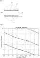
- FIG. 1 is a cross-sectional view showing a pellicle for extreme ultraviolet lithography containing molybdenum carbide according to a first embodiment of the present disclosure.
- FIG. 2 is an enlarged view of part A of FIG. 1 .
- a pellicle 100 for extreme ultraviolet lithography includes a substrate 10 having an opening 13 formed in its central portion, and a pellicle layer 30 formed on the substrate 10 so as to cover the opening 13 and including a molybdenum carbide containing layer that contains molybdenum carbide expressed as MoC 1-x (0 ⁇ x ⁇ 1).
- the pellicle layer 30 may include a core layer 31 and a capping layer 37 that are sequentially stacked on the substrate 10.
- the pellicle 100 according to the first embodiment may further include a support layer 20.
- the support layer 20 is interposed between the substrate 10 and the pellicle layer 30, and is formed on the substrate 10 to cover the opening 13.
- the pellicle 100 is a consumable component that protects a mask from contaminants in a lithography process for semiconductor or display manufacturing. That is, the pellicle 100 is a thin film overlying the mask and serves as a cover. Because the light transferred to the wafer is focused with the mask in a lithographic exposure, even if contaminants exist on the pellicle 100 that is separated by a certain distance, it is possible to minimize a problem of forming a defective pattern due to out of focus.
- the pellicle 100 may minimize defective patterns while protecting the mask from contaminants during the exposure process, thereby greatly increasing the yield of semiconductor or display manufacturing.
- the use of the pellicle 100 can increase the lifespan of the mask.
- the substrate 10 supports the support layer 20 and the pellicle layer 30 and makes it easy to handle and transport the pellicle 100 during and after the process of manufacturing the pellicle 100.
- the substrate 10 may be formed of a material such as silicon available for an etching process.
- the material of the substrate 10 includes, but is not limited to, silicon, silicon oxide, silicon nitride, metal oxide, metal nitride, graphite, amorphous carbon, or a laminated structure of such materials.
- metal may be, but is not limited to, Cr, Al, Zr, Ti, Ta, Nb, Ni, or the like.
- the support layer 20 serving as an etch stopper is formed on the substrate 10.
- the pellicle layer 30 is formed on the support layer 20.
- the support layer 20 is formed of a material having resistance to KOH, and also functions to prevent the material of the pellicle layer 30 from being diffused into the substrate 10.
- the material of the support layer 20 may include at least one of SiN x , SiO 2 , SiC, and Mo 2 C.
- SiN x may include Si 3 N 4 .
- the support layer 20 may be formed by a chemical vapor deposition (CVD) process, but it is formed by an atomic layer deposition (ALD), e-beam evaporation, or sputtering process so as to have the best transmittance and minimize defects through free control of thickness, physical properties, and chemical composition.
- the support layer 20 may be formed on the substrate 10 to have a thickness of 1 nm to 10 nm.
- the support layer 20 may be formed to have a thickness corresponding to the capping layer 37.
- the opening 13 in the central portion of the substrate 10 may be formed using a micro-machining technique such as micro-electro mechanical systems (MEMS). That is, the opening 13 is formed by removing the central portion of the substrate 10 under the support layer 20 by means of the micro-machining technique. The opening 13 partially exposes the etch stopper 20 under the pellicle layer 30.
- MEMS micro-electro mechanical systems
- the pellicle layer 30 includes the core layer 31 and the capping layer 37. At least one of the core layer 31 and the capping layer 37 is a molybdenum carbide containing layer.
- the core layer 31 is a layer that determines the transmittance of extreme ultraviolet rays.
- the core layer 31 has a transmittance of 90% or more for extreme ultraviolet rays, and effectively dissipates heat to prevent overheating of the pellicle layer 30.
- the capping layer 37 provides thermal stability, mechanical stability, and chemical durability to the pellicle layer 30 while minimizing a decrease in the transmittance of the core layer 31 for extreme ultraviolet rays.
- the capping layer 37 is a protective layer for the core layer 31 and provides thermal stability by effectively dissipating heat generated in the core layer 31 to the outside.
- the capping layer 37 provides mechanical stability by supplementing the mechanical strength of the core layer 31.
- the capping layer 37 provides chemical durability by protecting the core layer 31 from hydrogen radicals and oxidation.
- the molybdenum carbide containing layer is a binary material of molybdenum (Mo) and carbon (C) expressed as MoC 1-x (0 ⁇ x ⁇ 1) and can be easily manufactured using a deposition method.
- the molybdenum carbide containing layer may contain MoC 1-x (0.5 ⁇ x ⁇ 1) in which carbon and molybdenum having a valence of divalent or higher are combined.
- the molybdenum carbide containing layer may contain crystalline or amorphous Mo 2 C in the form of a mixture or, in part, grains.
- the molybdenum carbide containing layer may be a Mo 2 C layer composed of Mo 2 C.
- the molybdenum carbide containing layer can be prepared as a carbide at a lower temperature, for example, 700°C, than other carbides. That is, the temperature at which crystallization starts is 900°C for silicon carbide and 1000°C or more for zirconium carbide and boron carbide. However, because molybdenum carbide has a high bonding strength between molybdenum and carbon, carbide preparation begins at 700°C.
- Mo 2 C may be easily formed in a thin film through sputtering of Mo and then heat treatment in a hydrocarbon atmosphere or through sputtering of Mo 2 C target and then heat treatment in an inert gas atmosphere.
- Mo 2 C may be easily formed in a thin film through sputtering of Mo and then heat treatment in a hydrocarbon atmosphere or through sputtering of Mo 2 C target and then heat treatment in an inert gas atmosphere.
- the molybdenum carbide containing layer is capable of providing the pellicle 100 with high erosion and wear resistance, resistance to hydrogen radicals, and chemical stability at high temperatures.
- the molybdenum carbide containing layer can be used as an etch stopper in dry etching and wet etching environments for the production of a freestanding membrane because of the erosion resistance and chemical resistance of Mo 2 C.
- the core layer 31 may be the molybdenum carbide containing layer.
- the core layer 31 containing molybdenum carbide By forming the core layer 31 containing molybdenum carbide to a thickness of 18 nm or less, it is possible to provide a pellicle for extreme ultraviolet lithography having an extreme ultraviolet transmittance of 90% or more and a reflectance of 0.04% or less in an extreme ultraviolet output environment of 350W or more.
- the material of the capping layer 37 may include at least one of nitride, oxide, boride, carbide, and silicide.
- the nitride may include SiN x , SiON, BN, or BCN.
- the oxide may include SiO 2 .
- the boride may include ZrB x (2 ⁇ x ⁇ 16), ZrB x Si y (x ⁇ 2, y ⁇ 2), YB x (x ⁇ 2), or SiB 6 .
- the carbide may include SiC, Mo 2 C, or B 4 C.
- the silicide may include ZrSix (x ⁇ 2).
- the core layer 31 as the molybdenum carbide containing layer, it is possible to provide a pellicle for extreme ultraviolet lithography having an extreme ultraviolet transmittance of 90% or more and a reflectance of 0.04% or less in an extreme ultraviolet output environment of 350W or more.
- molybdenum carbide can be easily formed through a typical deposition process
- using molybdenum carbide as the material of the core layer 31 can simplify the manufacturing process of the core layer 31 than using graphene or a multi-component material.
- the capping layer 37 may be the molybdenum carbide containing layer.
- the capping layer 37 formed with the molybdenum carbide containing layer may have a thickness of 10 nm or less.
- the material of the core layer 31 may include at least one of graphene, Me- ⁇ (Me is at least one of Zr and Mo, and ⁇ is at least one of nitride, boride, carbide, and silicide), ZrSi 2 , ZrB x (2 ⁇ x ⁇ 16), ZrB x Si y (x ⁇ 2, y ⁇ 2), and YB x (x ⁇ 2).
- the core layer 31 When the core layer 31 is formed of graphene, it may be formed by a transfer method or a direct growth method.
- the transfer method is a method of forming the core layer 31 by transferring graphene grown on a separate substrate onto the support layer 20 of the substrate 10.
- the direct growth method is a method of directly growing graphene on the support layer 20 of the substrate 10 by using interlayer exchange between a metal catalyst layer and a source layer of an amorphous carbon material through heat treatment.
- the metal catalyst layer is removed after the graphene is directly grown.
- a seed layer may be formed on the support layer 20 so that graphene, which is directly grown through interlayer exchange, can be stably bonded on the support layer 20.
- At least one of an amorphous carbon layer formed to a thickness of 5 nm or less, few-layer graphene, amorphous boron, BN, BCN, B 4 C, and Me-X (Me is at least one of Si, Ti, Mo, and Zr, and X is at least one of B, C, and N) may be used.
- the above-described pellicle 100 according to the first embodiment may be manufactured by the following manufacturing process. First, the support layer 20, the core layer 31, and the capping layer 37 are sequentially stacked on the substrate 10 in which the opening 13 is not formed.
- the support layer 20 may be formed by a CVD, ALD, e-beam deposition, or sputtering process.
- the core layer 31 and the capping layer 37 may be formed using various deposition methods such as sputtering, CVD, and ALD.
- the molybdenum carbide containing layer included in the pellicle layer 30 may be formed by sputtering.
- a Mo thin film is deposited on the support layer 20 by sputtering. Then, by heat-treating the Mo thin film in an atmosphere containing hydrocarbon gas and hydrogen at a temperature of 700°C or higher, it is possible to form the Mo 2 C layer on the support layer.
- the pellicle 100 according to the first embodiment can be obtained. That is, the opening 13 is formed by removing the central portion of the substrate 10 under the support layer 20 through wet etching. The opening 13 partially exposes the support layer 20 under the core layer 31.
- FIG. 3 is an enlarged view showing a pellicle for extreme ultraviolet lithography containing molybdenum carbide according to a second embodiment of the present disclosure.
- the pellicle according to the second embodiment includes the substrate having the opening formed in the central portion, the support layer 20 formed on the substrate to cover the opening, and a pellicle layer 130 including a molybdenum carbide containing layer formed on the support layer 20.
- the pellicle layer 130 includes the core layer 31, a buffer layer 35, and the capping layer 37 that are sequentially stacked on the support layer 20.
- the buffer layer 35 may be formed with the molybdenum carbide containing layer that contains molybdenum carbide.
- Using the molybdenum carbide as the material of the buffer layer 35 can provide the pellicle according to the second embodiment having a stacked structure of the core layer 31 and the capping layer 37 of various materials.
- the material of the capping layer 37 may include at least one of nitride, oxide, boride, carbide, and silicide.
- the material of the core layer 31 may include at least one of graphene, Me- ⁇ (Me is at least one of Zr and Mo, and ⁇ is at least one of nitride, boride, carbide, and silicide), ZrSi 2 , ZrB x (2 ⁇ x ⁇ 16), ZrB x Si y (x ⁇ 2, y ⁇ 2), and YBX (x ⁇ 2).
- the buffer layer 35 contains molybdenum carbide
- the material of the buffer layer 35 may include at least one of B, C, Zr, B 4 C, BN, SiN x (x ⁇ 1), MoSi 2 , RuC, NbCx (0 ⁇ x ⁇ 1), YC x (0.5 ⁇ x ⁇ 2), ZrSi x (x ⁇ 2), ZrCx (0.3 ⁇ x ⁇ 1), ZrB x (2 ⁇ x ⁇ 16), ZrB x Si y (x ⁇ 2, y ⁇ 2), ZrC x B y (0.8 ⁇ x ⁇ 1.2, y ⁇ 2), and ZrCxSi (0.8 ⁇ x ⁇ 1.2, y ⁇ 2).
- C among the materials of the buffer layer 35 may include amorphous carbon, graphene, carbon nanotube
- the above-described pellicle according to the second embodiment may be manufactured by the following manufacturing process. First, the support layer 20, the core layer 31, the buffer layer 35, and the capping layer 37 are sequentially stacked on the substrate in which the opening is not formed.
- the support layer 20 may be formed by a CVD, ALD, e-beam deposition, or sputtering process.
- the core layer 31, the buffer layer 35, and the capping layer 37 may be formed using various deposition methods such as sputtering, CVD, and ALD.
- the molybdenum carbide containing layer included in the pellicle layer 30 may be formed by sputtering.
- a Mo thin film is deposited on the support layer 20 by sputtering. Then, by heat-treating the Mo thin film in an atmosphere containing hydrocarbon gas and hydrogen at a temperature of 700°C or higher, it is possible to form the Mo 2 C layer on the support layer.
- the pellicle according to the second embodiment can be obtained. That is, the opening 13 is formed by removing the central portion of the substrate 10 under the support layer 20 through wet etching. The opening 13 partially exposes the support layer 20 under the core layer 31.
- FIG. 4 is an enlarged view showing a pellicle for extreme ultraviolet lithography containing molybdenum carbide according to a third embodiment of the present disclosure.
- the pellicle according to the third embodiment includes the substrate having the opening formed in the central portion, the support layer 20 formed on the substrate to cover the opening, and a pellicle layer 230 containing molybdenum carbide formed on the support layer 20.
- the pellicle layer 230 includes a first buffer layer 33, the core layer 31, a second buffer layer 35, and the capping layer 37 that are sequentially stacked on the support layer 20.
- each of the first and second buffer layers 33 and 35 may be formed with a molybdenum carbide containing layer that contains molybdenum carbide.
- Using the molybdenum carbide as the materials of the first and second buffer layers 33 and 35 can provide the pellicle according to the third embodiment having a stacked structure of the core layer 31 and the capping layer 37 of various materials.
- the material of the capping layer 37 may include at least one of nitride, oxide, boride, carbide, and silicide.
- the material of the core layer 31 may include at least one of graphene, Me- ⁇ (Me is at least one of Zr and Mo, and ⁇ is at least one of nitride, boride, carbide, and silicide), ZrSi 2 , ZrB x (2 ⁇ x ⁇ 16), ZrB x Si y (x ⁇ 2, y ⁇ 2), and YB x (x ⁇ 2).
- the pellicle layer 230 according to the third embodiment an example in which the first and second buffer layers 33 and 35 contain molybdenum carbide is described, this is not construed as a limitation.
- the first or second buffer layer 33 or 35 may contain molybdenum carbide.
- the material of the first and second buffer layers 33 and 35 may include at least one of B, C, Zr, B 4 C, BN, SiN x (x ⁇ 1), MoSi 2 , RuC, NbCx (0 ⁇ x ⁇ 1), YCx (0.5 ⁇ x ⁇ 2), ZrSi x (x ⁇ 2), ZrCx (0.3 ⁇ x ⁇ 1), ZrB x (2 ⁇ x ⁇ 16), ZrB x Si y (x ⁇ 2, y ⁇ 2), ZrC x B y (0.8 ⁇ x ⁇ 1.2, y ⁇ 2), and ZrC x Si (0.8 ⁇ x ⁇ 1.2, y ⁇ 2).
- C among the materials of the buffer layer 35 may include amorphous carbon, graphene, carbon nanotube
- the above-described pellicle according to the third embodiment may be manufactured by the following manufacturing process. First, the support layer 20, the first buffer layer 33, the core layer 31, the second buffer layer 35, and the capping layer 37 are sequentially stacked on the substrate in which the opening is not formed.
- the support layer 20 may be formed by a CVD, ALD, e-beam deposition, or sputtering process.
- the first buffer layer 33, the core layer 31, the second buffer layer 35, and the capping layer 37 may be formed using various deposition methods such as sputtering, CVD, and ALD.
- the molybdenum carbide containing layer included in the pellicle layer 30 may be formed by sputtering.
- a Mo thin film is deposited on the support layer 20 by sputtering. Then, by heat-treating the Mo thin film in an atmosphere containing hydrocarbon gas and hydrogen at a temperature of 700°C or higher, it is possible to form the Mo 2 C layer on the support layer.
- the pellicle according to the third embodiment can be obtained. That is, the opening 13 is formed by removing the central portion of the substrate 10 under the support layer 20 through wet etching. The opening 13 partially exposes the support layer 20 under the core layer 31.
- the above-described pellicle according to the present disclosure can be used in a lithography process using a light source having a wavelength of 7 nm to 13.5 nm, or 190 nm or less.
- the pellicle according to the present disclosure can be free-standing by supporting the pellicle layer on a circular or rectangular frame having a diameter of 5 mm or more.
- FIGS. 5 to 14 are graphs showing transmittance and reflectance of pellicles according to first to fifth experimental examples of the present disclosure.
- the pellicle according to each of the first to fifth experimental examples includes the support layer, the core layer, and the capping layer.
- the materials of the support layer and the capping layer are SiN x .
- the material of the core layer is Mo 2 C.
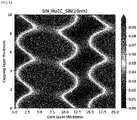
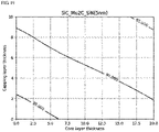
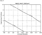
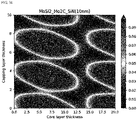
- the transmittance and reflectance of the pellicle according to each of the first to fifth experimental examples were simulated in an extreme ultraviolet output environment of 350W while changing the thickness of the core layer between 0 nm and 20 nm and the thickness of the capping layer between 0 nm and 10 nm.
- the pellicles according to the first to fifth experimental examples were expressed as "SiN_Mo2C_SiN(Xnm)".
- 'SiN(Xnm)' denotes the support layer
- Xnm denotes that the thickness of the support layer is 0 nm, 3 nm, 5 nm, 7 nm, or 10 nm.
- 'Mo2C' denotes the core layer
- 'SiN' denotes the capping layer.
- FIGS. 5 and 6 are graphs showing transmittance and reflectance of a pellicle for extreme ultraviolet lithography according to a first experimental example of the present disclosure.
- FIG. 5 shows the transmittance
- FIG. 6 shows the reflectance.
- the pellicle according to the first experimental example was expressed as "SiN_Mo2C_SiN(0nm)".
- the transmittance is 85% or more.
- the transmittance is 90% or more.
- the reflectance is 0.04% or less.
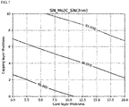
- FIGS. 7 and 8 are graphs showing transmittance and reflectance of a pellicle for extreme ultraviolet lithography according to a second experimental example of the present disclosure.
- FIG. 7 shows the transmittance
- FIG. 8 shows the reflectance.
- the pellicle according to the second experimental example was expressed as "SiN_Mo2C_SiN(3nm)".
- the transmittance is 85% or more.
- the transmittance is 90% or more.
- the thickness of the core layer is 10 to 17.5 nm and the thickness of the capping layer is 10 nm or less, it can be seen that the reflectance is 0.04% or less.
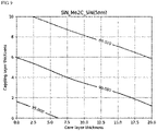
- FIGS. 9 and 10 are graphs showing transmittance and reflectance of a pellicle for extreme ultraviolet lithography according to a third experimental example of the present disclosure.
- FIG. 9 shows the transmittance
- FIG. 10 shows the reflectance.
- the pellicle according to the third experimental example was expressed as "SiN_Mo2C_SiN(5nm)".
- the transmittance is 85% or more.
- the transmittance is 90% or more.
- the reflectance is 0.04% or less.
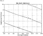
- FIGS. 11 and 12 are graphs showing transmittance and reflectance of a pellicle for extreme ultraviolet lithography according to a fourth experimental example of the present disclosure.
- FIG. 11 shows the transmittance
- FIG. 12 shows the reflectance.
- the pellicle according to the fourth experimental example was expressed as "SiN_Mo2C_SiN(7nm)".
- the transmittance is 85% or more.
- the transmittance is 90% or more.
- the reflectance is 0.04% or less.
- FIGS. 13 and 14 are graphs showing transmittance and reflectance of a pellicle for extreme ultraviolet lithography according to a fifth experimental example of the present disclosure.
- FIG. 13 shows the transmittance
- FIG. 14 shows the reflectance.
- the pellicle according to the fifth experimental example was expressed as "SiN_Mo2C_SiN(10nm)".
- the transmittance is 85% or more.
- the transmittance is 90% or more.
- the thickness of the core layer is 10 to 17.5 nm and the thickness of the capping layer is 10 nm or less, it can be seen that the reflectance is 0.04% or less.
- the capping layer is a SiN x layer and the core layer is a Mo 2 C layer
- FIGS. 15 to 24 are graphs showing transmittance and reflectance of pellicles according to sixth to tenth experimental examples of the present disclosure.
- the pellicle according to each of the sixth to tenth experimental examples includes the support layer, the core layer, and the capping layer.
- the material of the support layer is SiN x .
- the material of the core layer is Mo 2 C.
- the material of the capping layer is SiC.
- the transmittance and reflectance of the pellicle according to each of the sixth to tenth experimental examples were simulated in an extreme ultraviolet output environment of 350W while changing the thickness of the core layer between 0 nm and 20 nm and the thickness of the capping layer between 0 nm and 10 nm.
- the pellicles according to the sixth to tenth experimental examples were expressed as "SiC_Mo2C_SiN(Xnm)".
- 'SiN(Xnm)' denotes the support layer
- Xnm denotes that the thickness of the support layer is 0 nm, 3 nm, 5 nm, 7 nm, or 10 nm.
- 'Mo2C' denotes the core layer
- 'SiC' denotes the capping layer.
- FIGS. 15 and 16 are graphs showing transmittance and reflectance of a pellicle for extreme ultraviolet lithography according to a sixth experimental example of the present disclosure.
- FIG. 15 shows the transmittance
- FIG. 16 shows the reflectance.
- the pellicle according to the sixth experimental example was expressed as "SiC_Mo2C_SiN(0nm)".
- the transmittance is 90% or more.
- the reflectance is 0.04% or less.
- FIGS. 17 and 18 are graphs showing transmittance and reflectance of a pellicle for extreme ultraviolet lithography according to a seventh experimental example of the present disclosure.
- FIG. 17 shows the transmittance
- FIG. 18 shows the reflectance.
- the pellicle according to the seventh experimental example was expressed as "SiC_Mo2C_SiN(3nm)".
- the transmittance is 90% or more.
- the reflectance is 0.04% or less.
- FIGS. 19 and 20 are graphs showing transmittance and reflectance of a pellicle for extreme ultraviolet lithography according to an eighth experimental example of the present disclosure.
- FIG. 19 shows the transmittance
- FIG. 20 shows the reflectance.
- the pellicle according to the eighth experimental example was expressed as "SiC_Mo2C_SiN(5nm)".
- the transmittance is 90% or more.
- the reflectance is 0.04% or less.
- FIGS. 21 and 22 are graphs showing transmittance and reflectance of a pellicle for extreme ultraviolet lithography according to a ninth experimental example of the present disclosure.
- FIG. 21 shows the transmittance
- FIG. 22 shows the reflectance.
- the pellicle according to the ninth experimental example was expressed as "SiC_Mo2C_SiN(7nm)".
- the transmittance 90% or more.
- the reflectance is 0.04% or less.
- FIGS. 23 and 24 are graphs showing transmittance and reflectance of a pellicle for extreme ultraviolet lithography according to a tenth experimental example of the present disclosure.
- FIG. 23 shows the transmittance
- FIG. 24 shows the reflectance.
- the pellicle according to the tenth experimental example was expressed as "SiC_Mo2C_SiN(10nm)".
- the transmittance 90% or more.
- the reflectance is 0.04% or less.
- the capping layer is a SiC layer and the core layer is a Mo 2 C layer
- FIGS. 25 to 34 are graphs showing transmittance and reflectance of pellicles according to eleventh to fifteenth experimental examples of the present disclosure.
- the pellicle according to each of the eleventh to fifteenth experimental examples includes the support layer, the core layer, and the capping layer.
- the material of the support layer is SiN x .
- the material of the core layer is Mo 2 C.
- the material of the capping layer is MoSi 2 .
- the transmittance and reflectance of the pellicle according to each of the eleventh to fifteenth experimental examples were simulated in an extreme ultraviolet output environment of 350W while changing the thickness of the core layer between 0 nm and 20 nm and the thickness of the capping layer between 0 nm and 10 nm.
- the pellicles according to the eleventh to fifteenth experimental examples were expressed as "MoSi2_Mo2C_SiN(Xnm)".
- 'SiN(Xnm)' denotes the support layer
- Xnm denotes that the thickness of the support layer is 0 nm, 3 nm, 5 nm, 7 nm, or 10 nm.
- 'Mo2C' denotes the core layer
- 'MoSi2' denotes the capping layer.
- FIGS. 25 and 26 are graphs showing transmittance and reflectance of a pellicle for extreme ultraviolet lithography according to an eleventh experimental example of the present disclosure.
- FIG. 25 shows the transmittance
- FIG. 26 shows the reflectance.
- the pellicle according to the eleventh experimental example was expressed as "MoSi2_Mo2C_SiN(0nm)".
- the transmittance is 90% or more.
- the reflectance is 0.04% or less.
- FIGS. 27 and 28 are graphs showing transmittance and reflectance of a pellicle for extreme ultraviolet lithography according to a twelfth experimental example of the present disclosure.
- FIG. 27 shows the transmittance
- FIG. 28 shows the reflectance.
- the pellicle according to the twelfth experimental example was expressed as "MoSi2_Mo2C_SiN(3nm)".
- the transmittance is 90% or more.
- the reflectance is 0.04% or less discontinuously in the thickness of the capping layer of 10 nm or less.
- the thickness of the core layer is 12 to 15 nm and the thickness of the capping layer is 10 nm or less, it can be seen that the reflectance is 0.04% or less.
- FIGS. 29 and 30 are graphs showing transmittance and reflectance of a pellicle for extreme ultraviolet lithography according to a thirteenth experimental example of the present disclosure.
- FIG. 29 shows the transmittance
- FIG. 30 shows the reflectance.
- the pellicle according to the thirteenth experimental example was expressed as "MoSi2_Mo2C_SiN(5nm)".
- the transmittance is 90% or more.
- the reflectance is 0.04% or less discontinuously in the thickness of the capping layer of 10 nm or less.
- the thickness of the core layer is about 15 nm and the thickness of the capping layer is 10 nm or less, it can be seen that the reflectance is 0.04% or less.
- FIGS. 31 and 32 are graphs showing transmittance and reflectance of a pellicle for extreme ultraviolet lithography according to a fourteenth experimental example of the present disclosure.
- FIG. 31 shows the transmittance
- FIG. 32 shows the reflectance.
- the pellicle according to the fourteenth experimental example was expressed as "MoSi2_Mo2C_SiN(7nm)".
- the transmittance 90% or more.
- the reflectance is 0.04% or less.
- the reflectance is 0.04% or less discontinuously in the thickness of the capping layer of 10 nm or less.
- FIGS. 33 and 34 are graphs showing transmittance and reflectance of a pellicle for extreme ultraviolet lithography according to a fifteenth experimental example of the present disclosure.
- FIG. 33 shows the transmittance
- FIG. 34 shows the reflectance.
- the pellicle according to the fifteenth experimental example was expressed as "MoSi2_Mo2C_SiN(10nm)".
- the transmittance 90% or more.
- the reflectance is 0.04% or less discontinuously in the thickness of the capping layer of 10 nm or less.
- the thickness of the core layer is 13 to 15 nm and the thickness of the capping layer is 10 nm or less, it can be seen that the reflectance is 0.04% or less.
- the capping layer is a MoSi 2 layer and the core layer is a Mo 2 C layer
Landscapes
- Physics & Mathematics (AREA)
- General Physics & Mathematics (AREA)
- Preparing Plates And Mask In Photomechanical Process (AREA)
- Printing Plates And Materials Therefor (AREA)
Abstract
A pellicle for extreme ultraviolet lithography containing molybdenum carbide is disclosed. The pellicle includes a substrate having an opening formed in a central portion, and a pellicle layer formed on the substrate to cover the opening and including a molybdenum carbide containing layer that contains molybdenum carbide expressed as MoC<sub>1-x</sub> (0<x<1). The pellicle layer includes a core layer formed on the substrate to cover the opening, and the core layer may be the molybdenum carbide containing layer.
Description
- The present disclosure relates to a semiconductor lithography technology. More particularly, the present disclosure relates to a pellicle for extreme ultraviolet lithography containing molybdenum carbide and installed in a mask used in a lithography process using extreme ultraviolet rays.
- As the semiconductor industry continues to develop and the degree of semiconductor integration is dramatically improved, electronic devices are becoming smaller and lighter. In order to further improve the degree of semiconductor integration, the advancement of lithography technology is required.
- Currently, technology is developing toward realizing a fine pattern of a semiconductor by reducing the wavelength of light. Extreme ultraviolet (EUV) lithography technology, recently developed as a next-generation technology, can realize a fine pattern through a single resist process.
- An extreme ultraviolet lithography apparatus used in a semiconductor process includes a light source power, a resist, a pellicle, and a mask. The pellicle is installed on the mask to prevent contaminants generated during the lithography process from adhering to the mask, and is selectively used depending on the lithography machine.
- In the extreme ultraviolet lithography process, there was an expectation that the pellicle would not be needed because a clean system was built. However, it has been known that during an actual operation after the construction of the lithography apparatus, contamination of the mask is caused by foreign substances generated from an internal driving unit of the apparatus, particles of tin generated in the oscillation of the light source, and extreme ultraviolet photoresist.
- Therefore, in the extreme ultraviolet lithography process, the pellicle is recognized as an essential component so as to prevent contamination of the mask. When the pellicle is used, defects smaller than 10,000 nm in size are negligible.
- The pellicle for extreme ultraviolet lithography is required to have a size of 110 mm × 144 mm to cover the mask, and an extreme ultraviolet transmittance of 90% or more is required in order to minimize deterioration of productivity due to loss of a light source. In addition, mechanical stability that the pellicle is not damaged by physical movement up to 20G inside the extreme ultraviolet lithography apparatus, and thermal stability that the pellicle can withstand a thermal load of 250W or more based on a 5 nm node are required. Also, chemical durability that the pellicle does not react to hydrogen radicals generated in an extreme ultraviolet environment is required.
- Currently, pellicle development companies are developing transmissive materials based on polycrystalline silicon (p-Si) or SiN. However, such materials do not satisfy a transmittance of 90% or more, which is the most important condition of a pellicle for extreme ultraviolet lithography. Also, such materials have weaknesses in thermal stability, mechanical stability, and chemical durability in an extreme ultraviolet lithography environment, so that process development research is being conducted to supplement their properties. For example, materials such as Mo, Ru, and Zr have been selected and studied as materials for solving the problems of SiN-based materials, but it is difficult to manufacture a thin film and maintain its shape.
- Recently, a pellicle having an extreme ultraviolet transmittance of 90% or more and thermal, chemical, and mechanical stability in an extreme ultraviolet output environment of 350W or more, exceeding an irradiation intensity of 250W level, is required.
- The present disclosure provides a pellicle for extreme ultraviolet lithography containing molybdenum carbide having an extreme ultraviolet transmittance of 90% or more in an extreme ultraviolet output environment of 350W or more.
- In addition, the present disclosure provides a pellicle for extreme ultraviolet lithography containing molybdenum carbide having thermal stability, mechanical stability and chemical durability while having a high extreme ultraviolet transmittance of 90% or more.
- According to embodiments of the present disclosure, a pellicle for extreme ultraviolet lithography may include a substrate having an opening formed in a central portion, and a pellicle layer formed on the substrate to cover the opening and including a molybdenum carbide containing layer that contains molybdenum carbide expressed as MoC1-x (0<x<1). The pellicle layer may include a core layer formed on the substrate to cover the opening, and the core layer may be the molybdenum carbide containing layer.
- In the pellicle, the molybdenum carbide containing layer may contain crystalline or amorphous molybdenum carbide in a form of a mixture or, in part, grains.
- In the pellicle, the molybdenum carbide containing layer may contain Mo2C.
- In the pellicle, the pellicle layer may further include a capping layer formed on the core layer.
- In the pellicle, a material of the capping layer may include at least one of nitride, oxide, boride, carbide, and silicide.
- In the pellicle, the capping layer may contain molybdenum carbide.
- The pellicle may further include a support layer interposed between the substrate and the pellicle layer, formed on the substrate to cover the opening, and formed of a material including at least one of SiNx, SiO2, SiC, and Mo2C.
- In the pellicle, the pellicle layer may further include a capping layer formed on the core layer, and a buffer layer formed at least one of between the substrate and the core layer and between the core layer and the capping layer.
- In the pellicle, at least one of the capping layer and the buffer layer may contain molybdenum carbide.
- In the pellicle, when the buffer layer contains molybdenum carbide, a material of the capping layer may include at least one of nitride, oxide, boride, carbide, and silicide.
- In the pellicle, when the capping layer contains molybdenum carbide, a material of the buffer layer may include at least one of B, C, Zr, B4C, BN, SiNx (x≥1), MoSi2, RuC, NbCx (0<x≤1), YCx (0.5≤x≤2), ZrSix (x≤2), ZrCx (0.3≤x≤1), ZrBx (2<x<16), ZrBxSiy (x≥2, y≥2), ZrCxBy (0.8≤x≤1.2, y≥2), and ZrCxSi (0.8≤x≤1.2, y≤2).
- According to embodiments of the present disclosure, a pellicle for extreme ultraviolet lithography may include a pellicle layer including a molybdenum carbide containing layer that contains molybdenum carbide expressed as MoC1-x (0<x<1), the pellicle layer including a core layer formed on a substrate to cover an opening of the substrate, wherein the core layer is the molybdenum carbide containing layer.
- In the pellicle, the molybdenum carbide containing layer may contain crystalline or amorphous molybdenum carbide in a form of a mixture or, in part, grains.
- In the pellicle, the molybdenum carbide containing layer may contain Mo2C.
- In the pellicle, the pellicle layer may further include a capping layer formed on one surface or both surfaces of the core layer.
- In the pellicle, the capping layer may contain molybdenum carbide.
- In the pellicle, the pellicle layer may further include a buffer layer formed on one surface or both surfaces of the core layer, and a capping layer formed on the buffer layer, wherein at least one of the buffer layer and the capping layer contains molybdenum carbide.
- According to the present disclosure, by applying molybdenum carbide to the pellicle layer, it is possible to provide the pellicle for extreme ultraviolet lithography having an extreme ultraviolet transmittance of 90% or more and a reflectance of 0.04% or less in an extreme ultraviolet output environment of 350W or more. That is, by forming at least one of the core layer, the buffer layer, and the capping layer in the pellicle layer as the molybdenum carbide containing layer, the pellicle for extreme ultraviolet lithography can be provided to have an extreme ultraviolet transmittance of 90% or more and a reflectance of 0.04% or less in an extreme ultraviolet output environment of 350W or more.
- The molybdenum carbide containing layer is a binary material of molybdenum (Mo) and carbon (C) expressed as MoC1-x (0<x<1) and can be easily manufactured using a deposition method. In addition, the molybdenum carbide containing layer can be prepared as a carbide at a lower temperature, for example, 700°C, than other carbides.
- In a process of forming the molybdenum carbide containing layer, Mo2C may be easily formed in a thin film through sputtering of Mo and then heat treatment in a hydrocarbon atmosphere or through sputtering of Mo2C target and then heat treatment in an inert gas atmosphere. When the molybdenum carbide containing layer is formed through sputtering, it is also advantageous to control the thickness uniformity.
- The molybdenum carbide containing layer contains crystalline or amorphous Mo2C in the form of a mixture or, in part, grains, and, as a carbide, is capable of providing the pellicle with high erosion and wear resistance, resistance to hydrogen radicals, and chemical stability at high temperatures.
- In addition, the molybdenum carbide containing layer can be used as an etch stopper in dry etching and wet etching environments for the production of a freestanding membrane because of the erosion resistance and chemical resistance of Mo2C.
-
-
FIG. 1 is a cross-sectional view showing a pellicle for extreme ultraviolet lithography containing molybdenum carbide according to a first embodiment of the present disclosure. -
FIG. 2 is an enlarged view of part A ofFIG. 1 . -
FIG. 3 is an enlarged view showing a pellicle for extreme ultraviolet lithography containing molybdenum carbide according to a second embodiment of the present disclosure. -
FIG. 4 is an enlarged view showing a pellicle for extreme ultraviolet lithography containing molybdenum carbide according to a third embodiment of the present disclosure. -
FIGS. 5 and6 are graphs showing transmittance and reflectance of a pellicle for extreme ultraviolet lithography according to a first experimental example of the present disclosure. -
FIGS. 7 and8 are graphs showing transmittance and reflectance of a pellicle for extreme ultraviolet lithography according to a second experimental example of the present disclosure. -
FIGS. 9 and10 are graphs showing transmittance and reflectance of a pellicle for extreme ultraviolet lithography according to a third experimental example of the present disclosure. -
FIGS. 11 and12 are graphs showing transmittance and reflectance of a pellicle for extreme ultraviolet lithography according to a fourth experimental example of the present disclosure. -
FIGS. 13 and14 are graphs showing transmittance and reflectance of a pellicle for extreme ultraviolet lithography according to a fifth experimental example of the present disclosure. -
FIGS. 15 and16 are graphs showing transmittance and reflectance of a pellicle for extreme ultraviolet lithography according to a sixth experimental example of the present disclosure. -
FIGS. 17 and18 are graphs showing transmittance and reflectance of a pellicle for extreme ultraviolet lithography according to a seventh experimental example of the present disclosure. -
FIGS. 19 and20 are graphs showing transmittance and reflectance of a pellicle for extreme ultraviolet lithography according to an eighth experimental example of the present disclosure. -
FIGS. 21 and22 are graphs showing transmittance and reflectance of a pellicle for extreme ultraviolet lithography according to a ninth experimental example of the present disclosure. -
FIGS. 23 and24 are graphs showing transmittance and reflectance of a pellicle for extreme ultraviolet lithography according to a tenth experimental example of the present disclosure. -
FIGS. 25 and26 are graphs showing transmittance and reflectance of a pellicle for extreme ultraviolet lithography according to an eleventh experimental example of the present disclosure. -
FIGS. 27 and28 are graphs showing transmittance and reflectance of a pellicle for extreme ultraviolet lithography according to a twelfth experimental example of the present disclosure. -
FIGS. 29 and30 are graphs showing transmittance and reflectance of a pellicle for extreme ultraviolet lithography according to a thirteenth experimental example of the present disclosure. -
FIGS. 31 and32 are graphs showing transmittance and reflectance of a pellicle for extreme ultraviolet lithography according to a fourteenth experimental example of the present disclosure. -
FIGS. 33 and34 are graphs showing transmittance and reflectance of a pellicle for extreme ultraviolet lithography according to a fifteenth experimental example of the present disclosure. - Hereinafter, an embodiment of the present disclosure will be described in detail with reference to the accompanying drawings. The present disclosure may, however, be embodied in many different forms and should not be construed as being limited to the embodiment set forth herein. Rather, this embodiment is provided so that the disclosure will be thorough and complete and will fully convey the scope of the disclosure to those skilled in the art. Accordingly, an embodiment described herein should be understood to include various modifications, equivalents, and/or alternatives.
- In addition, techniques that are well known in the art and not directly related to the present disclosure are not described herein. This is to clearly convey the subject matter of the present disclosure by omitting an unnecessary explanation. Also, the terms are merely used for describing a particular embodiment but do not limit the embodiment. Singular forms are intended to include plural forms unless the context clearly indicates otherwise.
-
FIG. 1 is a cross-sectional view showing a pellicle for extreme ultraviolet lithography containing molybdenum carbide according to a first embodiment of the present disclosure.FIG. 2 is an enlarged view of part A ofFIG. 1 . - Referring to
FIGS. 1 and 2 , apellicle 100 for extreme ultraviolet lithography according to the first embodiment (hereinafter referred to as 'pellicle') includes asubstrate 10 having anopening 13 formed in its central portion, and apellicle layer 30 formed on thesubstrate 10 so as to cover theopening 13 and including a molybdenum carbide containing layer that contains molybdenum carbide expressed as MoC1-x (0<x<1). Thepellicle layer 30 may include acore layer 31 and acapping layer 37 that are sequentially stacked on thesubstrate 10. - The
pellicle 100 according to the first embodiment may further include asupport layer 20. Thesupport layer 20 is interposed between thesubstrate 10 and thepellicle layer 30, and is formed on thesubstrate 10 to cover theopening 13. - The
pellicle 100 is a consumable component that protects a mask from contaminants in a lithography process for semiconductor or display manufacturing. That is, thepellicle 100 is a thin film overlying the mask and serves as a cover. Because the light transferred to the wafer is focused with the mask in a lithographic exposure, even if contaminants exist on thepellicle 100 that is separated by a certain distance, it is possible to minimize a problem of forming a defective pattern due to out of focus. - As such, the
pellicle 100 may minimize defective patterns while protecting the mask from contaminants during the exposure process, thereby greatly increasing the yield of semiconductor or display manufacturing. In addition, the use of thepellicle 100 can increase the lifespan of the mask. - Now, the
pellicle 100 according to the present disclosure will be described in detail. - The
substrate 10 supports thesupport layer 20 and thepellicle layer 30 and makes it easy to handle and transport thepellicle 100 during and after the process of manufacturing thepellicle 100. Thesubstrate 10 may be formed of a material such as silicon available for an etching process. For example, the material of thesubstrate 10 includes, but is not limited to, silicon, silicon oxide, silicon nitride, metal oxide, metal nitride, graphite, amorphous carbon, or a laminated structure of such materials. Here, metal may be, but is not limited to, Cr, Al, Zr, Ti, Ta, Nb, Ni, or the like. - The
support layer 20 serving as an etch stopper is formed on thesubstrate 10. Thepellicle layer 30 is formed on thesupport layer 20. - The
support layer 20 is formed of a material having resistance to KOH, and also functions to prevent the material of thepellicle layer 30 from being diffused into thesubstrate 10. The material of thesupport layer 20 may include at least one of SiNx, SiO2, SiC, and Mo2C. Here, SiNx may include Si3N4. Thesupport layer 20 may be formed by a chemical vapor deposition (CVD) process, but it is formed by an atomic layer deposition (ALD), e-beam evaporation, or sputtering process so as to have the best transmittance and minimize defects through free control of thickness, physical properties, and chemical composition. Thesupport layer 20 may be formed on thesubstrate 10 to have a thickness of 1 nm to 10 nm. Thesupport layer 20 may be formed to have a thickness corresponding to thecapping layer 37. - The
opening 13 in the central portion of thesubstrate 10 may be formed using a micro-machining technique such as micro-electro mechanical systems (MEMS). That is, theopening 13 is formed by removing the central portion of thesubstrate 10 under thesupport layer 20 by means of the micro-machining technique. Theopening 13 partially exposes theetch stopper 20 under thepellicle layer 30. - The
pellicle layer 30 includes thecore layer 31 and thecapping layer 37. At least one of thecore layer 31 and thecapping layer 37 is a molybdenum carbide containing layer. - The
core layer 31 is a layer that determines the transmittance of extreme ultraviolet rays. Thecore layer 31 has a transmittance of 90% or more for extreme ultraviolet rays, and effectively dissipates heat to prevent overheating of thepellicle layer 30. - The
capping layer 37 provides thermal stability, mechanical stability, and chemical durability to thepellicle layer 30 while minimizing a decrease in the transmittance of thecore layer 31 for extreme ultraviolet rays. Specifically, thecapping layer 37 is a protective layer for thecore layer 31 and provides thermal stability by effectively dissipating heat generated in thecore layer 31 to the outside. In addition, thecapping layer 37 provides mechanical stability by supplementing the mechanical strength of thecore layer 31. In addition, thecapping layer 37 provides chemical durability by protecting thecore layer 31 from hydrogen radicals and oxidation. - The molybdenum carbide containing layer is a binary material of molybdenum (Mo) and carbon (C) expressed as MoC1-x (0<x<1) and can be easily manufactured using a deposition method. The molybdenum carbide containing layer may contain MoC1-x (0.5≤x<1) in which carbon and molybdenum having a valence of divalent or higher are combined. The molybdenum carbide containing layer may contain crystalline or amorphous Mo2C in the form of a mixture or, in part, grains. The molybdenum carbide containing layer may be a Mo2C layer composed of Mo2C.
- The molybdenum carbide containing layer can be prepared as a carbide at a lower temperature, for example, 700°C, than other carbides. That is, the temperature at which crystallization starts is 900°C for silicon carbide and 1000°C or more for zirconium carbide and boron carbide. However, because molybdenum carbide has a high bonding strength between molybdenum and carbon, carbide preparation begins at 700°C.
- In a process of forming the molybdenum carbide containing layer, Mo2C may be easily formed in a thin film through sputtering of Mo and then heat treatment in a hydrocarbon atmosphere or through sputtering of Mo2C target and then heat treatment in an inert gas atmosphere. When the molybdenum carbide containing layer is formed through sputtering, it is also advantageous to control the thickness uniformity.
- The molybdenum carbide containing layer, as a carbide, is capable of providing the
pellicle 100 with high erosion and wear resistance, resistance to hydrogen radicals, and chemical stability at high temperatures. - In addition, the molybdenum carbide containing layer can be used as an etch stopper in dry etching and wet etching environments for the production of a freestanding membrane because of the erosion resistance and chemical resistance of Mo2C.
- First, the
core layer 31 may be the molybdenum carbide containing layer. By forming thecore layer 31 containing molybdenum carbide to a thickness of 18 nm or less, it is possible to provide a pellicle for extreme ultraviolet lithography having an extreme ultraviolet transmittance of 90% or more and a reflectance of 0.04% or less in an extreme ultraviolet output environment of 350W or more. - With respect to the
core layer 31 containing molybdenum carbide, the material of thecapping layer 37 may include at least one of nitride, oxide, boride, carbide, and silicide. Here, the nitride may include SiNx, SiON, BN, or BCN. The oxide may include SiO2. The boride may include ZrBx (2≤x<16), ZrBxSiy (x≥2, y≥2), YBx (x≥2), or SiB6. The carbide may include SiC, Mo2C, or B4C. The silicide may include ZrSix (x≥2). - As such, by forming the
core layer 31 as the molybdenum carbide containing layer, it is possible to provide a pellicle for extreme ultraviolet lithography having an extreme ultraviolet transmittance of 90% or more and a reflectance of 0.04% or less in an extreme ultraviolet output environment of 350W or more. - In addition, because molybdenum carbide can be easily formed through a typical deposition process, using molybdenum carbide as the material of the
core layer 31 can simplify the manufacturing process of thecore layer 31 than using graphene or a multi-component material. - Next, the
capping layer 37 may be the molybdenum carbide containing layer. Thecapping layer 37 formed with the molybdenum carbide containing layer may have a thickness of 10 nm or less. - With respect to the
capping layer 37 formed with the molybdenum carbide containing layer, the material of thecore layer 31 may include at least one of graphene, Me-α (Me is at least one of Zr and Mo, and α is at least one of nitride, boride, carbide, and silicide), ZrSi2, ZrBx (2≤x<16), ZrBxSiy (x≥2, y≥2), and YBx (x≥2). - When the
core layer 31 is formed of graphene, it may be formed by a transfer method or a direct growth method. - The transfer method is a method of forming the
core layer 31 by transferring graphene grown on a separate substrate onto thesupport layer 20 of thesubstrate 10. - The direct growth method is a method of directly growing graphene on the
support layer 20 of thesubstrate 10 by using interlayer exchange between a metal catalyst layer and a source layer of an amorphous carbon material through heat treatment. Of course, the metal catalyst layer is removed after the graphene is directly grown. A seed layer may be formed on thesupport layer 20 so that graphene, which is directly grown through interlayer exchange, can be stably bonded on thesupport layer 20. As the seed layer, at least one of an amorphous carbon layer formed to a thickness of 5 nm or less, few-layer graphene, amorphous boron, BN, BCN, B4C, and Me-X (Me is at least one of Si, Ti, Mo, and Zr, and X is at least one of B, C, and N) may be used. - The above-described
pellicle 100 according to the first embodiment may be manufactured by the following manufacturing process. First, thesupport layer 20, thecore layer 31, and thecapping layer 37 are sequentially stacked on thesubstrate 10 in which theopening 13 is not formed. - At this time, the
support layer 20 may be formed by a CVD, ALD, e-beam deposition, or sputtering process. - The
core layer 31 and thecapping layer 37 may be formed using various deposition methods such as sputtering, CVD, and ALD. - The molybdenum carbide containing layer included in the
pellicle layer 30 may be formed by sputtering. For example, in case that a Mo2C layer is formed as the molybdenum carbide containing layer, a Mo thin film is deposited on thesupport layer 20 by sputtering. Then, by heat-treating the Mo thin film in an atmosphere containing hydrocarbon gas and hydrogen at a temperature of 700°C or higher, it is possible to form the Mo2C layer on the support layer. - Thereafter, by removing the central portion of the
substrate 10 under thecore layer 31 to form theopening 13 through which thecore layer 31 is partially exposed, thepellicle 100 according to the first embodiment can be obtained. That is, theopening 13 is formed by removing the central portion of thesubstrate 10 under thesupport layer 20 through wet etching. Theopening 13 partially exposes thesupport layer 20 under thecore layer 31. -
FIG. 3 is an enlarged view showing a pellicle for extreme ultraviolet lithography containing molybdenum carbide according to a second embodiment of the present disclosure. - Referring to
FIG. 3 , the pellicle according to the second embodiment includes the substrate having the opening formed in the central portion, thesupport layer 20 formed on the substrate to cover the opening, and apellicle layer 130 including a molybdenum carbide containing layer formed on thesupport layer 20. Thepellicle layer 130 includes thecore layer 31, abuffer layer 35, and thecapping layer 37 that are sequentially stacked on thesupport layer 20. - In the
pellicle layer 130 according to the second embodiment, thebuffer layer 35 may be formed with the molybdenum carbide containing layer that contains molybdenum carbide. - Using the molybdenum carbide as the material of the
buffer layer 35 can provide the pellicle according to the second embodiment having a stacked structure of thecore layer 31 and thecapping layer 37 of various materials. - With respect to the
buffer layer 35 formed with the molybdenum carbide containing layer, the material of thecapping layer 37 may include at least one of nitride, oxide, boride, carbide, and silicide. The material of thecore layer 31 may include at least one of graphene, Me-α (Me is at least one of Zr and Mo, and α is at least one of nitride, boride, carbide, and silicide), ZrSi2, ZrBx (2≤x<16), ZrBxSiy (x≥2, y≥2), and YBX (x≥2). - Meanwhile, although in the
pellicle layer 130 according to the second embodiment an example in which thebuffer layer 35 contains molybdenum carbide is described, this is not construed as a limitation. - Alternatively or additionally, in the
pellicle layer 130 according to the second embodiment, at least one of thecore layer 31 and thecapping layer 37 may contain molybdenum carbide as in the first embodiment. When thecore layer 31 or thecapping layer 37 is formed with the molybdenum carbide containing layer, the material of thebuffer layer 35 may include at least one of B, C, Zr, B4C, BN, SiNx (x≥1), MoSi2, RuC, NbCx (0<x≤1), YCx (0.5≤x≤2), ZrSix (x≤2), ZrCx (0.3≤x≤1), ZrBx (2<x<16), ZrBxSiy (x≥2, y≥2), ZrCxBy (0.8≤x≤1.2, y≥2), and ZrCxSi (0.8≤x≤1.2, y≤2). Here, C among the materials of thebuffer layer 35 may include amorphous carbon, graphene, carbon nanotubes, SiC, or the like. - The above-described pellicle according to the second embodiment may be manufactured by the following manufacturing process. First, the
support layer 20, thecore layer 31, thebuffer layer 35, and thecapping layer 37 are sequentially stacked on the substrate in which the opening is not formed. - At this time, the
support layer 20 may be formed by a CVD, ALD, e-beam deposition, or sputtering process. - The
core layer 31, thebuffer layer 35, and thecapping layer 37 may be formed using various deposition methods such as sputtering, CVD, and ALD. - The molybdenum carbide containing layer included in the
pellicle layer 30 may be formed by sputtering. For example, in case that a Mo2C layer is formed as the molybdenum carbide containing layer, a Mo thin film is deposited on thesupport layer 20 by sputtering. Then, by heat-treating the Mo thin film in an atmosphere containing hydrocarbon gas and hydrogen at a temperature of 700°C or higher, it is possible to form the Mo2C layer on the support layer. - Thereafter, by removing the central portion of the
substrate 10 under thecore layer 31 to form theopening 13 through which thecore layer 31 is partially exposed, the pellicle according to the second embodiment can be obtained. That is, theopening 13 is formed by removing the central portion of thesubstrate 10 under thesupport layer 20 through wet etching. Theopening 13 partially exposes thesupport layer 20 under thecore layer 31. -
FIG. 4 is an enlarged view showing a pellicle for extreme ultraviolet lithography containing molybdenum carbide according to a third embodiment of the present disclosure. - Referring to
FIG. 4 , the pellicle according to the third embodiment includes the substrate having the opening formed in the central portion, thesupport layer 20 formed on the substrate to cover the opening, and apellicle layer 230 containing molybdenum carbide formed on thesupport layer 20. Thepellicle layer 230 includes afirst buffer layer 33, thecore layer 31, asecond buffer layer 35, and thecapping layer 37 that are sequentially stacked on thesupport layer 20. - In the
pellicle layer 230 according to the third embodiment, each of the first and second buffer layers 33 and 35 may be formed with a molybdenum carbide containing layer that contains molybdenum carbide. - Using the molybdenum carbide as the materials of the first and second buffer layers 33 and 35 can provide the pellicle according to the third embodiment having a stacked structure of the
core layer 31 and thecapping layer 37 of various materials. - With respect to the first and second buffer layers 33 and 35 formed with the molybdenum carbide containing layer, the material of the
capping layer 37 may include at least one of nitride, oxide, boride, carbide, and silicide. The material of thecore layer 31 may include at least one of graphene, Me-α (Me is at least one of Zr and Mo, and α is at least one of nitride, boride, carbide, and silicide), ZrSi2, ZrBx (2≤x<16), ZrBxSiy (x≥2, y≥2), and YBx (x≥2). - Meanwhile, although in the
pellicle layer 230 according to the third embodiment an example in which the first and second buffer layers 33 and 35 contain molybdenum carbide is described, this is not construed as a limitation. - For example, the first or
second buffer layer - Alternatively or additionally, in the
pellicle layer 230, at least one of thecore layer 31 and thecapping layer 37 may contain molybdenum carbide as in the first embodiment. When thecore layer 31 or thecapping layer 37 is formed with the molybdenum carbide containing layer, the material of the first and second buffer layers 33 and 35 may include at least one of B, C, Zr, B4C, BN, SiNx (x≥1), MoSi2, RuC, NbCx (0<x≤1), YCx (0.5≤x≤2), ZrSix (x≤2), ZrCx (0.3≤x≤1), ZrBx (2<x<16), ZrBxSiy (x≥2, y≥2), ZrCxBy (0.8≤x≤1.2, y≥2), and ZrCxSi (0.8≤x≤1.2, y≤2). Here, C among the materials of thebuffer layer 35 may include amorphous carbon, graphene, carbon nanotubes, SiC, or the like. - The above-described pellicle according to the third embodiment may be manufactured by the following manufacturing process. First, the
support layer 20, thefirst buffer layer 33, thecore layer 31, thesecond buffer layer 35, and thecapping layer 37 are sequentially stacked on the substrate in which the opening is not formed. - At this time, the
support layer 20 may be formed by a CVD, ALD, e-beam deposition, or sputtering process. - The
first buffer layer 33, thecore layer 31, thesecond buffer layer 35, and thecapping layer 37 may be formed using various deposition methods such as sputtering, CVD, and ALD. - The molybdenum carbide containing layer included in the
pellicle layer 30 may be formed by sputtering. For example, in case that a Mo2C layer is formed as the molybdenum carbide containing layer, a Mo thin film is deposited on thesupport layer 20 by sputtering. Then, by heat-treating the Mo thin film in an atmosphere containing hydrocarbon gas and hydrogen at a temperature of 700°C or higher, it is possible to form the Mo2C layer on the support layer. - Thereafter, by removing the central portion of the
substrate 10 under thecore layer 31 to form theopening 13 through which thecore layer 31 is partially exposed, the pellicle according to the third embodiment can be obtained. That is, theopening 13 is formed by removing the central portion of thesubstrate 10 under thesupport layer 20 through wet etching. Theopening 13 partially exposes thesupport layer 20 under thecore layer 31. - The above-described pellicle according to the present disclosure can be used in a lithography process using a light source having a wavelength of 7 nm to 13.5 nm, or 190 nm or less.
- In addition, the pellicle according to the present disclosure can be free-standing by supporting the pellicle layer on a circular or rectangular frame having a diameter of 5 mm or more.
- In order to check the transmittance and reflectance of the pellicle according to the present disclosure in an extreme ultraviolet output environment of 350W or more, simulations were performed on the pellicles according to first to fifteenth experimental examples as shown in
FIGS. 5 to 34 . -
FIGS. 5 to 14 are graphs showing transmittance and reflectance of pellicles according to first to fifth experimental examples of the present disclosure. The pellicle according to each of the first to fifth experimental examples includes the support layer, the core layer, and the capping layer. The materials of the support layer and the capping layer are SiNx. The material of the core layer is Mo2C. - When the thickness of the support layer is 0 nm, 3 nm, 5 nm, 7 nm, or 10 nm, the transmittance and reflectance of the pellicle according to each of the first to fifth experimental examples were simulated in an extreme ultraviolet output environment of 350W while changing the thickness of the core layer between 0 nm and 20 nm and the thickness of the capping layer between 0 nm and 10 nm.
- The pellicles according to the first to fifth experimental examples were expressed as "SiN_Mo2C_SiN(Xnm)". Here, 'SiN(Xnm)' denotes the support layer, and Xnm denotes that the thickness of the support layer is 0 nm, 3 nm, 5 nm, 7 nm, or 10 nm. Also, 'Mo2C' denotes the core layer, and 'SiN' denotes the capping layer.
-
FIGS. 5 and6 are graphs showing transmittance and reflectance of a pellicle for extreme ultraviolet lithography according to a first experimental example of the present disclosure.FIG. 5 shows the transmittance, andFIG. 6 shows the reflectance. - Referring to
FIGS. 5 and6 , the pellicle according to the first experimental example was expressed as "SiN_Mo2C_SiN(0nm)". - When the thickness of the core layer is 20 nm or less and the thickness of the capping layer is 10 nm or less, the transmittance is 85% or more. When the thickness of the core layer is 20 nm or less and the thickness of the capping layer is 9 nm or less, it can be seen that the transmittance is 90% or more.
- In addition, when the thickness of the core layer is 12 to 17.5 nm and the thickness of the capping layer is 10 nm or less, it can be seen that the reflectance is 0.04% or less.
-
FIGS. 7 and8 are graphs showing transmittance and reflectance of a pellicle for extreme ultraviolet lithography according to a second experimental example of the present disclosure.FIG. 7 shows the transmittance, andFIG. 8 shows the reflectance. - Referring to
FIGS. 7 and8 , the pellicle according to the second experimental example was expressed as "SiN_Mo2C_SiN(3nm)". - When the thickness of the core layer is 20 nm or less and the thickness of the capping layer is 10 nm or less, the transmittance is 85% or more. When the thickness of the core layer is 20 nm or less and the thickness of the capping layer is 7 nm or less, it can be seen that the transmittance is 90% or more.
- In addition, when the thickness of the core layer is 10 to 17.5 nm and the thickness of the capping layer is 10 nm or less, it can be seen that the reflectance is 0.04% or less.
-
FIGS. 9 and10 are graphs showing transmittance and reflectance of a pellicle for extreme ultraviolet lithography according to a third experimental example of the present disclosure.FIG. 9 shows the transmittance, andFIG. 10 shows the reflectance. - Referring to
FIGS. 9 and10 , the pellicle according to the third experimental example was expressed as "SiN_Mo2C_SiN(5nm)". - When the thickness of the core layer is 20 nm or less and the thickness of the capping layer is 10 nm or less, the transmittance is 85% or more. When the thickness of the core layer is 20 nm or less and the thickness of the capping layer is 6 nm or less, it can be seen that the transmittance is 90% or more.
- In addition, when the thickness of the core layer is 12 to 19 nm and the thickness of the capping layer is 10 nm or less, it can be seen that the reflectance is 0.04% or less.
-
FIGS. 11 and12 are graphs showing transmittance and reflectance of a pellicle for extreme ultraviolet lithography according to a fourth experimental example of the present disclosure.FIG. 11 shows the transmittance, andFIG. 12 shows the reflectance. - Referring to
FIGS. 11 and12 , the pellicle according to the fourth experimental example was expressed as "SiN_Mo2C_SiN(7nm)". - When the thickness of the core layer is 20 nm or less and the thickness of the capping layer is 10 nm or less, the transmittance is 85% or more. When the thickness of the core layer is 20 nm or less and the thickness of the capping layer is 5 nm or less, it can be seen that the transmittance is 90% or more.
- In addition, when the thickness of the core layer is 12 to 17.5 nm and the thickness of the capping layer is 10 nm or less, it can be seen that the reflectance is 0.04% or less.
-
FIGS. 13 and14 are graphs showing transmittance and reflectance of a pellicle for extreme ultraviolet lithography according to a fifth experimental example of the present disclosure.FIG. 13 shows the transmittance, andFIG. 14 shows the reflectance. - Referring to
FIGS. 13 and14 , the pellicle according to the fifth experimental example was expressed as "SiN_Mo2C_SiN(10nm)". - When the thickness of the core layer is 20 nm or less and the thickness of the capping layer is 8 nm or less, the transmittance is 85% or more. When the thickness of the core layer is 15 nm or less and the thickness of the capping layer is 3 nm or less, it can be seen that the transmittance is 90% or more.
- In addition, when the thickness of the core layer is 10 to 17.5 nm and the thickness of the capping layer is 10 nm or less, it can be seen that the reflectance is 0.04% or less.
- As such, according to the first to fifth experimental examples, in case that the capping layer is a SiNx layer and the core layer is a Mo2C layer, it can be seen that it is possible to provide a pellicle having an extreme ultraviolet transmittance of 90% or more and a reflectance of 0.04% or less when the thickness of the core layer is formed to be 17.5 nm or less.
-
FIGS. 15 to 24 are graphs showing transmittance and reflectance of pellicles according to sixth to tenth experimental examples of the present disclosure. The pellicle according to each of the sixth to tenth experimental examples includes the support layer, the core layer, and the capping layer. The material of the support layer is SiNx. The material of the core layer is Mo2C. The material of the capping layer is SiC. - When the thickness of the support layer is 0 nm, 3 nm, 5 nm, 7 nm, or 10 nm, the transmittance and reflectance of the pellicle according to each of the sixth to tenth experimental examples were simulated in an extreme ultraviolet output environment of 350W while changing the thickness of the core layer between 0 nm and 20 nm and the thickness of the capping layer between 0 nm and 10 nm.
- The pellicles according to the sixth to tenth experimental examples were expressed as "SiC_Mo2C_SiN(Xnm)". Here, 'SiN(Xnm)' denotes the support layer, and Xnm denotes that the thickness of the support layer is 0 nm, 3 nm, 5 nm, 7 nm, or 10 nm. Also, 'Mo2C' denotes the core layer, and 'SiC' denotes the capping layer.
-
FIGS. 15 and16 are graphs showing transmittance and reflectance of a pellicle for extreme ultraviolet lithography according to a sixth experimental example of the present disclosure.FIG. 15 shows the transmittance, andFIG. 16 shows the reflectance. - Referring to
FIGS. 15 and16 , the pellicle according to the sixth experimental example was expressed as "SiC_Mo2C_SiN(0nm)". - When the thickness of the core layer is 20 nm or less and the thickness of the capping layer is 10 nm or less, it can be seen that the transmittance is 90% or more.
- In addition, when the thickness of the core layer is 12 to 17 nm and the thickness of the capping layer is 10 nm or less, it can be seen that the reflectance is 0.04% or less.
-
FIGS. 17 and18 are graphs showing transmittance and reflectance of a pellicle for extreme ultraviolet lithography according to a seventh experimental example of the present disclosure.FIG. 17 shows the transmittance, andFIG. 18 shows the reflectance. - Referring to
FIGS. 17 and18 , the pellicle according to the seventh experimental example was expressed as "SiC_Mo2C_SiN(3nm)". - When the thickness of the core layer is 20 nm or less and the thickness of the capping layer is 10 nm or less, it can be seen that the transmittance is 90% or more.
- In addition, when the thickness of the core layer is 10 to 17 nm and the thickness of the capping layer is 10 nm or less, it can be seen that the reflectance is 0.04% or less.
-
FIGS. 19 and20 are graphs showing transmittance and reflectance of a pellicle for extreme ultraviolet lithography according to an eighth experimental example of the present disclosure.FIG. 19 shows the transmittance, andFIG. 20 shows the reflectance. - Referring to
FIGS. 19 and20 , the pellicle according to the eighth experimental example was expressed as "SiC_Mo2C_SiN(5nm)". - When the thickness of the core layer is 20 nm or less and the thickness of the capping layer is 9 nm or less, it can be seen that the transmittance is 90% or more.
- In addition, when the thickness of the core layer is 12 to 19 nm and the thickness of the capping layer is 10 nm or less, it can be seen that the reflectance is 0.04% or less.
-
FIGS. 21 and22 are graphs showing transmittance and reflectance of a pellicle for extreme ultraviolet lithography according to a ninth experimental example of the present disclosure.FIG. 21 shows the transmittance, andFIG. 22 shows the reflectance. - Referring to
FIGS. 21 and22 , the pellicle according to the ninth experimental example was expressed as "SiC_Mo2C_SiN(7nm)". - When the thickness of the core layer is 20 nm or less and the thickness of the capping layer is 8 nm or less, it can be seen that the transmittance is 90% or more.
- In addition, when the thickness of the core layer is 12 to 17 nm and the thickness of the capping layer is 10 nm or less, it can be seen that the reflectance is 0.04% or less.
-
FIGS. 23 and24 are graphs showing transmittance and reflectance of a pellicle for extreme ultraviolet lithography according to a tenth experimental example of the present disclosure.FIG. 23 shows the transmittance, andFIG. 24 shows the reflectance. - Referring to
FIGS. 23 and24 , the pellicle according to the tenth experimental example was expressed as "SiC_Mo2C_SiN(10nm)". - When the thickness of the core layer is 15 nm or less and the thickness of the capping layer is 5 nm or less, it can be seen that the transmittance is 90% or more.
- In addition, when the thickness of the core layer is 10 to 17 nm and the thickness of the capping layer is 10 nm or less, it can be seen that the reflectance is 0.04% or less.
- As such, according to the sixth to tenth experimental examples, in case that the capping layer is a SiC layer and the core layer is a Mo2C layer, it can be seen that it is possible to provide a pellicle having an extreme ultraviolet transmittance of 90% or more and a reflectance of 0.04% or less when the thickness of the core layer is formed to be about 15 nm.
-
FIGS. 25 to 34 are graphs showing transmittance and reflectance of pellicles according to eleventh to fifteenth experimental examples of the present disclosure. The pellicle according to each of the eleventh to fifteenth experimental examples includes the support layer, the core layer, and the capping layer. The material of the support layer is SiNx. The material of the core layer is Mo2C. The material of the capping layer is MoSi2. - When the thickness of the support layer is 0 nm, 3 nm, 5 nm, 7 nm, or 10 nm, the transmittance and reflectance of the pellicle according to each of the eleventh to fifteenth experimental examples were simulated in an extreme ultraviolet output environment of 350W while changing the thickness of the core layer between 0 nm and 20 nm and the thickness of the capping layer between 0 nm and 10 nm.
- The pellicles according to the eleventh to fifteenth experimental examples were expressed as "MoSi2_Mo2C_SiN(Xnm)". Here, 'SiN(Xnm)' denotes the support layer, and Xnm denotes that the thickness of the support layer is 0 nm, 3 nm, 5 nm, 7 nm, or 10 nm. Also, 'Mo2C' denotes the core layer, and 'MoSi2' denotes the capping layer.
-
FIGS. 25 and26 are graphs showing transmittance and reflectance of a pellicle for extreme ultraviolet lithography according to an eleventh experimental example of the present disclosure.FIG. 25 shows the transmittance, andFIG. 26 shows the reflectance. - Referring to
FIGS. 25 and26 , the pellicle according to the eleventh experimental example was expressed as "MoSi2_Mo2C_SiN(0nm)". - When the thickness of the core layer is 20 nm or less and the thickness of the capping layer is 10 nm or less, it can be seen that the transmittance is 90% or more.
- In addition, when the thickness of the core layer is 11 to 17 nm and the thickness of the capping layer is 10 nm or less, it can be seen that the reflectance is 0.04% or less.
-
FIGS. 27 and28 are graphs showing transmittance and reflectance of a pellicle for extreme ultraviolet lithography according to a twelfth experimental example of the present disclosure.FIG. 27 shows the transmittance, andFIG. 28 shows the reflectance. - Referring to
FIGS. 27 and28 , the pellicle according to the twelfth experimental example was expressed as "MoSi2_Mo2C_SiN(3nm)". - When the thickness of the core layer is 20 nm or less and the thickness of the capping layer is 10 nm or less, it can be seen that the transmittance is 90% or more.
- In addition, when the thickness of the core layer is 12 to 20 nm, it can be seen that the reflectance is 0.04% or less discontinuously in the thickness of the capping layer of 10 nm or less. When the thickness of the core layer is 12 to 15 nm and the thickness of the capping layer is 10 nm or less, it can be seen that the reflectance is 0.04% or less.
-
FIGS. 29 and30 are graphs showing transmittance and reflectance of a pellicle for extreme ultraviolet lithography according to a thirteenth experimental example of the present disclosure.FIG. 29 shows the transmittance, andFIG. 30 shows the reflectance. - Referring to
FIGS. 29 and30 , the pellicle according to the thirteenth experimental example was expressed as "MoSi2_Mo2C_SiN(5nm)". - When the thickness of the core layer is 20 nm or less and the thickness of the capping layer is 10 nm or less, it can be seen that the transmittance is 90% or more.
- In addition, when the thickness of the core layer is 8 to 20 nm, it can be seen that the reflectance is 0.04% or less discontinuously in the thickness of the capping layer of 10 nm or less. When the thickness of the core layer is about 15 nm and the thickness of the capping layer is 10 nm or less, it can be seen that the reflectance is 0.04% or less.
-
FIGS. 31 and32 are graphs showing transmittance and reflectance of a pellicle for extreme ultraviolet lithography according to a fourteenth experimental example of the present disclosure.FIG. 31 shows the transmittance, andFIG. 32 shows the reflectance. - Referring to
FIGS. 31 and32 , the pellicle according to the fourteenth experimental example was expressed as "MoSi2_Mo2C_SiN(7nm)". - When the thickness of the core layer is 20 nm or less and the thickness of the capping layer is 8 nm or less, it can be seen that the transmittance is 90% or more.
- In addition, when the thickness of the core layer is 11 to 18 nm and the thickness of the capping layer is 10 nm or less, it can be seen that the reflectance is 0.04% or less.
- Also, when the thickness of the core layer is 11 to 18 nm, it can be seen that the reflectance is 0.04% or less discontinuously in the thickness of the capping layer of 10 nm or less.
-
FIGS. 33 and34 are graphs showing transmittance and reflectance of a pellicle for extreme ultraviolet lithography according to a fifteenth experimental example of the present disclosure.FIG. 33 shows the transmittance, andFIG. 34 shows the reflectance. - Referring to
FIGS. 33 and34 , the pellicle according to the fifteenth experimental example was expressed as "MoSi2_Mo2C_SiN(10nm)". - When the thickness of the core layer is 15 nm or less and the thickness of the capping layer is 6 nm or less, it can be seen that the transmittance is 90% or more.
- In addition, when the thickness of the core layer is 8 to 20 nm, it can be seen that the reflectance is 0.04% or less discontinuously in the thickness of the capping layer of 10 nm or less. When the thickness of the core layer is 13 to 15 nm and the thickness of the capping layer is 10 nm or less, it can be seen that the reflectance is 0.04% or less.
- As such, according to the eleventh to fifteenth experimental examples, in case that the capping layer is a MoSi2 layer and the core layer is a Mo2C layer, it can be seen that it is possible to provide a pellicle having an extreme ultraviolet transmittance of 90% or more and a reflectance of 0.04% or less when the thickness of the core layer is formed to be about 15 nm.
- While the present disclosure has been particularly shown and described with reference to an exemplary embodiment thereof, it will be understood by those skilled in the art that various changes in form and details may be made therein without departing from the scope of the present disclosure as defined by the appended claims.
Claims (17)
- A pellicle for extreme ultraviolet lithography, the pellicle comprising:a substrate having an opening formed in a central portion; anda pellicle layer formed on the substrate to cover the opening and including a molybdenum carbide containing layer that contains molybdenum carbide expressed as MoC1-x (0<x<1),the pellicle layer including:a core layer formed on the substrate to cover the opening,wherein the core layer is the molybdenum carbide containing layer.
- The pellicle of claim 1, wherein the molybdenum carbide containing layer contains crystalline or amorphous molybdenum carbide in a form of a mixture or, in part, grains.
- The pellicle of claim 1, wherein the molybdenum carbide containing layer contains Mo2C.
- The pellicle of claim 1, wherein the pellicle layer further includes:
a capping layer formed on the core layer. - The pellicle of claim 4, wherein a material of the capping layer includes at least one of nitride, oxide, boride, carbide, and silicide.
- The pellicle of claim 4, wherein the capping layer contains molybdenum carbide.
- The pellicle of claim 1, further comprising:
a support layer interposed between the substrate and the pellicle layer, formed on the substrate to cover the opening, and formed of a material including at least one of SiNx, SiO2, SiC, and Mo2C. - The pellicle of claim 1, wherein the pellicle layer further includes:a capping layer formed on the core layer; anda buffer layer formed at least one of between the substrate and the core layer and between the core layer and the capping layer.
- The pellicle of claim 8, wherein at least one of the capping layer and the buffer layer contains molybdenum carbide.
- The pellicle of claim 9, wherein when the buffer layer contains molybdenum carbide, a material of the capping layer includes at least one of nitride, oxide, boride, carbide, and silicide.
- The pellicle of claim 9, wherein when the capping layer contains molybdenum carbide, a material of the buffer layer includes at least one of B, C, Zr, B4C, BN, SiNx (x≥1), MoSi2, RuC, NbCx (0<x≤1), YCx (0.5≤x≤2), ZrSix (x≤2), ZrCx (0.3≤x≤1), ZrBx (2<x<16), ZrBxSiy (x≥2, y≥2), ZrCxBy (0.8≤x≤1.2, y≥2), and ZrCxSi (0.8≤x≤1.2, y≤2).
- A pellicle for extreme ultraviolet lithography, the pellicle comprising:a pellicle layer including a molybdenum carbide containing layer that contains molybdenum carbide expressed as MoC1-x (0<x<1),the pellicle layer including:a core layer formed on a substrate to cover an opening of the substrate,wherein the core layer is the molybdenum carbide containing layer.
- The pellicle of claim 12, wherein the molybdenum carbide containing layer contains crystalline or amorphous molybdenum carbide in a form of a mixture or, in part, grains.
- The pellicle of claim 12, wherein the molybdenum carbide containing layer contains Mo2C.
- The pellicle of claim 12, wherein the pellicle layer further includes:
a capping layer formed on one surface or both surfaces of the core layer. - The pellicle of claim 15, wherein the capping layer contains molybdenum carbide.
- The pellicle of claim 12, wherein the pellicle layer further includes:a buffer layer formed on one surface or both surfaces of the core layer; anda capping layer formed on the buffer layer,wherein at least one of the buffer layer and the capping layer contains molybdenum carbide.
Applications Claiming Priority (1)
| Application Number | Priority Date | Filing Date | Title |
|---|---|---|---|
| KR1020210046187A KR102676228B1 (en) | 2021-04-09 | 2021-04-09 | Pellicle for extreme ultraviolet lithography containing molybdenum carbide |
Publications (1)
| Publication Number | Publication Date |
|---|---|
| EP4071552A1 true EP4071552A1 (en) | 2022-10-12 |
Family
ID=80780499
Family Applications (1)
| Application Number | Title | Priority Date | Filing Date |
|---|---|---|---|
| EP22162246.7A Pending EP4071552A1 (en) | 2021-04-09 | 2022-03-15 | Molybdenum-carbide-containing pellicle for extreme ultraviolet lithography |
Country Status (5)
| Country | Link |
|---|---|
| US (1) | US12326658B2 (en) |
| EP (1) | EP4071552A1 (en) |
| JP (1) | JP7428745B2 (en) |
| KR (2) | KR102676228B1 (en) |
| TW (1) | TWI862908B (en) |
Families Citing this family (2)
| Publication number | Priority date | Publication date | Assignee | Title |
|---|---|---|---|---|
| KR102897940B1 (en) * | 2023-02-16 | 2025-12-09 | 한국전자기술연구원 | Nanotube-based pellicle for EUV photolithography and manufacturing method thereof |
| KR20240142787A (en) | 2023-03-22 | 2024-10-02 | 한국전자기술연구원 | Manufacturing method of porous Mo2C thin film and pellicle for extreme ultraviolet lithography using the same |
Citations (4)
| Publication number | Priority date | Publication date | Assignee | Title |
|---|---|---|---|---|
| DE102017202861A1 (en) * | 2017-02-22 | 2017-04-13 | Carl Zeiss Smt Gmbh | Projection exposure machine with multifunctional pellicle and process for producing the projection exposure apparatus |
| US20190056654A1 (en) * | 2015-10-22 | 2019-02-21 | Asml Netherlands B.V. | Method of manufacturing a pellicle for a lithographic apparatus, a pellicle for a lithographic apparatus, a lithographic apparatus, a device manufacturing method, an apparatus for processing a pellicle, and a method for processing a pellicle |
| WO2020008976A1 (en) * | 2018-07-06 | 2020-01-09 | 株式会社カネカ | Pellicular complex and method for producing same |
| US20200406244A1 (en) * | 2018-03-09 | 2020-12-31 | Asml Netherlands B.V. | Graphene pellicle lithographic apparatus |
Family Cites Families (6)
| Publication number | Priority date | Publication date | Assignee | Title |
|---|---|---|---|---|
| KR102560643B1 (en) * | 2014-07-04 | 2023-07-27 | 에이에스엠엘 네델란즈 비.브이. | Membranes for use within a lithographic apparatus and a lithographic apparatus comprising such a membrane |
| KR102797693B1 (en) * | 2015-12-14 | 2025-04-17 | 에이에스엠엘 네델란즈 비.브이. | A membrane for euv lithography |
| US10908496B2 (en) | 2016-04-25 | 2021-02-02 | Asml Netherlands B.V. | Membrane for EUV lithography |
| US11016383B2 (en) | 2018-08-31 | 2021-05-25 | Taiwan Semiconductor Manufacturing Co., Ltd. | Pellicle for an EUV lithography mask and a method of manufacturing thereof |
| KR20200126216A (en) * | 2019-04-29 | 2020-11-06 | 주식회사 에스앤에스텍 | Pellicle for Extreme Ultraviolet(EUV) Lithography and method for fabricating of the same |
| KR20200141913A (en) * | 2019-06-11 | 2020-12-21 | 주식회사 에스앤에스텍 | Pellicle with improved wrinkle, and method for manufacturing the same |
-
2021
- 2021-04-09 KR KR1020210046187A patent/KR102676228B1/en active Active
-
2022
- 2022-03-15 EP EP22162246.7A patent/EP4071552A1/en active Pending
- 2022-03-18 US US17/698,427 patent/US12326658B2/en active Active
- 2022-03-29 TW TW111111949A patent/TWI862908B/en active
- 2022-04-08 JP JP2022064475A patent/JP7428745B2/en active Active
-
2024
- 2024-06-11 KR KR1020240075653A patent/KR20240085914A/en not_active Ceased
Patent Citations (4)
| Publication number | Priority date | Publication date | Assignee | Title |
|---|---|---|---|---|
| US20190056654A1 (en) * | 2015-10-22 | 2019-02-21 | Asml Netherlands B.V. | Method of manufacturing a pellicle for a lithographic apparatus, a pellicle for a lithographic apparatus, a lithographic apparatus, a device manufacturing method, an apparatus for processing a pellicle, and a method for processing a pellicle |
| DE102017202861A1 (en) * | 2017-02-22 | 2017-04-13 | Carl Zeiss Smt Gmbh | Projection exposure machine with multifunctional pellicle and process for producing the projection exposure apparatus |
| US20200406244A1 (en) * | 2018-03-09 | 2020-12-31 | Asml Netherlands B.V. | Graphene pellicle lithographic apparatus |
| WO2020008976A1 (en) * | 2018-07-06 | 2020-01-09 | 株式会社カネカ | Pellicular complex and method for producing same |
Also Published As
| Publication number | Publication date |
|---|---|
| TW202248754A (en) | 2022-12-16 |
| TWI862908B (en) | 2024-11-21 |
| KR20240085914A (en) | 2024-06-17 |
| KR102676228B1 (en) | 2024-06-18 |
| US12326658B2 (en) | 2025-06-10 |
| JP2022161891A (en) | 2022-10-21 |
| JP7428745B2 (en) | 2024-02-06 |
| KR20220140105A (en) | 2022-10-18 |
| US20220326603A1 (en) | 2022-10-13 |
Similar Documents
| Publication | Publication Date | Title |
|---|---|---|
| US12321092B2 (en) | Pellicle for extreme ultraviolet lithography containing amorphous carbon and method for manufacturing the same | |
| US11789359B2 (en) | Method for manufacturing pellicle for extreme ultraviolet lithography having graphene defect healing layer | |
| KR102739482B1 (en) | Method for manufacturing a pellicle for a lithography apparatus, pellicle device for a lithography apparatus, lithography apparatus, device manufacturing method, pellicle processing apparatus, and pellicle processing method | |
| US12248243B2 (en) | Multilayer graphene direct growth method and method for manufacturing pellicle for extreme ultraviolet lithography using the same | |
| US11927881B2 (en) | Pellicle for extreme ultraviolet lithography based on yttrium carbide | |
| US12326658B2 (en) | Pellicle for extreme ultraviolet lithography containing molybdenum carbide | |
| US12287568B2 (en) | Low-temperature direct growth method of multilayer graphene, pellicle for extreme ultraviolet lithography using the same, and method for manufacturing the pellicle | |
| KR102715190B1 (en) | Pellicle for extreme ultraviolet lithography based on yttrium | |
| US12379654B2 (en) | Pellicle for extreme ultraviolet lithography | |
| KR102715191B1 (en) | Pellicle for extreme ultraviolet lithography using metal carbide nanowire | |
| KR102755315B1 (en) | Pellicle for extreme ultraviolet lithography based on nibium carbide | |
| KR102897940B1 (en) | Nanotube-based pellicle for EUV photolithography and manufacturing method thereof | |
| KR20220141374A (en) | Pellicle for extreme ultraviolet lithography containing yttrium compounds |
Legal Events
| Date | Code | Title | Description |
|---|---|---|---|
| PUAI | Public reference made under article 153(3) epc to a published international application that has entered the european phase |
Free format text: ORIGINAL CODE: 0009012 |
|
| STAA | Information on the status of an ep patent application or granted ep patent |
Free format text: STATUS: REQUEST FOR EXAMINATION WAS MADE |
|
| 17P | Request for examination filed |
Effective date: 20220315 |
|
| AK | Designated contracting states |
Kind code of ref document: A1 Designated state(s): AL AT BE BG CH CY CZ DE DK EE ES FI FR GB GR HR HU IE IS IT LI LT LU LV MC MK MT NL NO PL PT RO RS SE SI SK SM TR |
|
| RBV | Designated contracting states (corrected) |
Designated state(s): AL AT BE BG CH CY CZ DE DK EE ES FI FR GB GR HR HU IE IS IT LI LT LU LV MC MK MT NL NO PL PT RO RS SE SI SK SM TR |