EP4070945A1 - Metallized film and film capacitor using same - Google Patents
Metallized film and film capacitor using same Download PDFInfo
- Publication number
- EP4070945A1 EP4070945A1 EP20897412.1A EP20897412A EP4070945A1 EP 4070945 A1 EP4070945 A1 EP 4070945A1 EP 20897412 A EP20897412 A EP 20897412A EP 4070945 A1 EP4070945 A1 EP 4070945A1
- Authority
- EP
- European Patent Office
- Prior art keywords
- film
- metalized
- dielectric film
- height
- arithmetic mean
- Prior art date
- Legal status (The legal status is an assumption and is not a legal conclusion. Google has not performed a legal analysis and makes no representation as to the accuracy of the status listed.)
- Withdrawn
Links
Images

Classifications
-
- B—PERFORMING OPERATIONS; TRANSPORTING
- B32—LAYERED PRODUCTS
- B32B—LAYERED PRODUCTS, i.e. PRODUCTS BUILT-UP OF STRATA OF FLAT OR NON-FLAT, e.g. CELLULAR OR HONEYCOMB, FORM
- B32B27/00—Layered products comprising a layer of synthetic resin
- B32B27/28—Layered products comprising a layer of synthetic resin comprising synthetic resins not wholly covered by any one of the sub-groups B32B27/30 - B32B27/42
-
- H—ELECTRICITY
- H01—ELECTRIC ELEMENTS
- H01G—CAPACITORS; CAPACITORS, RECTIFIERS, DETECTORS, SWITCHING DEVICES, LIGHT-SENSITIVE OR TEMPERATURE-SENSITIVE DEVICES OF THE ELECTROLYTIC TYPE
- H01G4/00—Fixed capacitors; Processes of their manufacture
- H01G4/002—Details
- H01G4/018—Dielectrics
- H01G4/06—Solid dielectrics
- H01G4/14—Organic dielectrics
- H01G4/18—Organic dielectrics of synthetic material, e.g. derivatives of cellulose
-
- B—PERFORMING OPERATIONS; TRANSPORTING
- B32—LAYERED PRODUCTS
- B32B—LAYERED PRODUCTS, i.e. PRODUCTS BUILT-UP OF STRATA OF FLAT OR NON-FLAT, e.g. CELLULAR OR HONEYCOMB, FORM
- B32B27/00—Layered products comprising a layer of synthetic resin
- B32B27/06—Layered products comprising a layer of synthetic resin as the main or only constituent of a layer, which is next to another layer of the same or of a different material
- B32B27/08—Layered products comprising a layer of synthetic resin as the main or only constituent of a layer, which is next to another layer of the same or of a different material of synthetic resin
-
- B—PERFORMING OPERATIONS; TRANSPORTING
- B32—LAYERED PRODUCTS
- B32B—LAYERED PRODUCTS, i.e. PRODUCTS BUILT-UP OF STRATA OF FLAT OR NON-FLAT, e.g. CELLULAR OR HONEYCOMB, FORM
- B32B3/00—Layered products comprising a layer with external or internal discontinuities or unevennesses, or a layer of non-planar shape; Layered products comprising a layer having particular features of form
- B32B3/02—Layered products comprising a layer with external or internal discontinuities or unevennesses, or a layer of non-planar shape; Layered products comprising a layer having particular features of form characterised by features of form at particular places, e.g. in edge regions
- B32B3/08—Layered products comprising a layer with external or internal discontinuities or unevennesses, or a layer of non-planar shape; Layered products comprising a layer having particular features of form characterised by features of form at particular places, e.g. in edge regions characterised by added members at particular parts
-
- H—ELECTRICITY
- H01—ELECTRIC ELEMENTS
- H01G—CAPACITORS; CAPACITORS, RECTIFIERS, DETECTORS, SWITCHING DEVICES, LIGHT-SENSITIVE OR TEMPERATURE-SENSITIVE DEVICES OF THE ELECTROLYTIC TYPE
- H01G4/00—Fixed capacitors; Processes of their manufacture
- H01G4/002—Details
- H01G4/005—Electrodes
- H01G4/012—Form of non-self-supporting electrodes
-
- H—ELECTRICITY
- H01—ELECTRIC ELEMENTS
- H01G—CAPACITORS; CAPACITORS, RECTIFIERS, DETECTORS, SWITCHING DEVICES, LIGHT-SENSITIVE OR TEMPERATURE-SENSITIVE DEVICES OF THE ELECTROLYTIC TYPE
- H01G4/00—Fixed capacitors; Processes of their manufacture
- H01G4/32—Wound capacitors
-
- B—PERFORMING OPERATIONS; TRANSPORTING
- B32—LAYERED PRODUCTS
- B32B—LAYERED PRODUCTS, i.e. PRODUCTS BUILT-UP OF STRATA OF FLAT OR NON-FLAT, e.g. CELLULAR OR HONEYCOMB, FORM
- B32B2250/00—Layers arrangement
- B32B2250/24—All layers being polymeric
-
- B—PERFORMING OPERATIONS; TRANSPORTING
- B32—LAYERED PRODUCTS
- B32B—LAYERED PRODUCTS, i.e. PRODUCTS BUILT-UP OF STRATA OF FLAT OR NON-FLAT, e.g. CELLULAR OR HONEYCOMB, FORM
- B32B2255/00—Coating on the layer surface
- B32B2255/10—Coating on the layer surface on synthetic resin layer or on natural or synthetic rubber layer
-
- B—PERFORMING OPERATIONS; TRANSPORTING
- B32—LAYERED PRODUCTS
- B32B—LAYERED PRODUCTS, i.e. PRODUCTS BUILT-UP OF STRATA OF FLAT OR NON-FLAT, e.g. CELLULAR OR HONEYCOMB, FORM
- B32B2255/00—Coating on the layer surface
- B32B2255/20—Inorganic coating
-
- B—PERFORMING OPERATIONS; TRANSPORTING
- B32—LAYERED PRODUCTS
- B32B—LAYERED PRODUCTS, i.e. PRODUCTS BUILT-UP OF STRATA OF FLAT OR NON-FLAT, e.g. CELLULAR OR HONEYCOMB, FORM
- B32B2307/00—Properties of the layers or laminate
- B32B2307/20—Properties of the layers or laminate having particular electrical or magnetic properties, e.g. piezoelectric
- B32B2307/204—Di-electric
-
- B—PERFORMING OPERATIONS; TRANSPORTING
- B32—LAYERED PRODUCTS
- B32B—LAYERED PRODUCTS, i.e. PRODUCTS BUILT-UP OF STRATA OF FLAT OR NON-FLAT, e.g. CELLULAR OR HONEYCOMB, FORM
- B32B2307/00—Properties of the layers or laminate
- B32B2307/70—Other properties
- B32B2307/732—Dimensional properties
-
- B—PERFORMING OPERATIONS; TRANSPORTING
- B32—LAYERED PRODUCTS
- B32B—LAYERED PRODUCTS, i.e. PRODUCTS BUILT-UP OF STRATA OF FLAT OR NON-FLAT, e.g. CELLULAR OR HONEYCOMB, FORM
- B32B2457/00—Electrical equipment
- B32B2457/16—Capacitors
-
- H—ELECTRICITY
- H01—ELECTRIC ELEMENTS
- H01G—CAPACITORS; CAPACITORS, RECTIFIERS, DETECTORS, SWITCHING DEVICES, LIGHT-SENSITIVE OR TEMPERATURE-SENSITIVE DEVICES OF THE ELECTROLYTIC TYPE
- H01G4/00—Fixed capacitors; Processes of their manufacture
- H01G4/002—Details
- H01G4/005—Electrodes
- H01G4/015—Special provisions for self-healing
Definitions
- the present disclosure relates to a metalized film and a film capacitor including the metalized film.
- Patent Literature 1 A known technique is described in, for example, Patent Literature 1.
- Patent Literature 1 Japanese Patent No. 6120180
- a metalized film includes a dielectric film having a first surface and a second surface opposite to the first surface.
- the dielectric film has a film thickness of 1 to 3 ⁇ m.
- the first surface has an arithmetic mean height Sa1.
- the second surface has an arithmetic mean height Sa2.
- the arithmetic mean height Sa1 and the arithmetic mean height Sa2 are different.
- the first surface has a maximum height Sz1 satisfying the expression 100 nm ⁇ Sz1 ⁇ 350 nm.
- the second surface has a maximum height Sz2 satisfying the expression 10 nm ⁇ Sz2 ⁇ 100 nm.
- the metalized film includes a metal film on the second surface.
- a film capacitor with the structure that forms the basis of a film capacitor according to one or more embodiments of the present disclosure includes either a wound metalized film or metalized films stacked in a predetermined direction.
- the wound metalized film or the metalized films stacked are formed by vapor deposition of metal films on a surface of a dielectric film of, for example, a polypropylene resin.
- a film capacitor that has short-circuited in a defective insulating portion of its dielectric film can self-recover the insulation in the defective insulating portion by causing a metal film portion around the defective insulating portion to diffuse using energy resulting from the short-circuiting.
- Such film capacitors are thus less likely to undergo dielectric breakdown and have increasingly been used in, for example, motors for driving hybrid electric vehicles (HEVs) or electric vehicles (EVs) and inverter systems for solar cell devices.
- the withstand voltage and the element processability of the film capacitor depend on the surface properties of a dielectric film included in the metalized film.
- a known metalized film can lower the withstand voltage of the film capacitor or the yield in manufacturing the film capacitor.
- a metalized film used in one or more embodiments of the present disclosure will now be described.
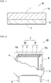
- a metalized film 10 in the present embodiment includes a dielectric film 1 and a metal film 2.
- the dielectric film 1 has a first surface 1a and a second surface 1b opposite to the first surface 1a.
- the dielectric film 1 has a film thickness of 1 to 3 ⁇ m.
- the dielectric film 1 is formed from an insulating resin.
- insulating materials for the dielectric film 1 include polypropylene (PP), polyethylene terephthalate (PET), polyphenylene sulfide (PPS), polyethylene naphthalate (PEN), polyarylate (PAR), polyphenylene ether (PPE), polyetherimide (PEI), and cycloolefin polymers (COP).
- an arithmetic mean height Sa1 of the first surface 1a and an arithmetic mean height Sa2 of the second surface 1b are different.
- the arithmetic mean height Sa1 and the arithmetic mean height Sa2 may be expressed using a 10-point average.
- the dielectric film 1 has a maximum height Sz1 of the first surface 1a satisfying the expression 100 nm ⁇ Sz1 ⁇ 350 nm, and a maximum height Sz2 of the second surface 1b satisfying the expression 10 nm ⁇ Sz2 ⁇ 100 nm. More specifically, the dielectric film 1 has the different maximum heights Sz1 and Sz2, which satisfy the expression 110 nm ⁇ Sz1 + Sz2 ⁇ 450 nm.
- the maximum heights Sz1 and Sz2 may be maximum heights of 10 points.
- the metal film 2 is formed from a metal material and is formed on the second surface 1b of the dielectric film 1.
- the metal material for the metal film 2 include aluminum and an aluminum-based alloy.
- the metal film 2 has a film thickness of, for example, 10 to 30 nm.
- the metalized film 10 may include, at one end of the dielectric film 1 in the width direction (perpendicular to the page of FIG. 1 ), a metal film-free portion 10a in which the metal film 2 is not deposited and the second surface 1b of the dielectric film 1 is exposed.
- the metal film-free portion 10a may extend continuously in the longitudinal direction of the dielectric film (lateral direction in FIG. 1 ).
- the metalized film 10 can be prepared as described below.
- the insulating resin is first dissolved in a solvent to prepare a resin solution.
- the solvent include methanol, isopropanol, n-butanol, ethylene glycol, ethylene glycol monopropyl ether, methyl ethyl ketone, methyl isobutyl ketone, xylene, propylene glycol monomethyl ether, propylene glycol monomethyl ether acetate, dimethylacetamide, cyclohexane, toluene, and a mixture of two or more solvents selected from these solvents.
- a base formed from, for example, PET is prepared, and a first main surface (also referred to as a third surface) of the base is blasted using alumina particles.
- the third surface may have a maximum height Sz3 in a range satisfying 100 nm ⁇ Sz3 ⁇ 350 nm.
- the resin solution is then shaped into a sheet on the third surface of the base.
- the method for shaping may be selected as appropriate from known methods including doctor blading, die coating, and knife coating.
- the resin solution applied onto the third surface is dried and the solvent is volatilized. This allows the base to include the dielectric film 1 on its third surface.
- the dielectric film 1 is separated from the base.
- the dielectric film 1 is then wound around a winding core, which is formed from resin or metal, and is collected.
- the metalized film 10 can be manufactured by vapor deposition of the metal film 2 onto the second surface 1b of the collected dielectric film 1.
- the dielectric film 1 formed on the third surface of the base is not wound around the winding core together with the base, but is separated from the base and wound around the winding core and is collected. This reduces indentations on the first surface 1a of the dielectric film 1 resulting from a second main surface of the base pressed against the first surface 1a.
- the first surface 1a of the dielectric film 1, on which the metal film 2 is not deposited has fine irregularities that satisfy the expression 100 nm ⁇ Sz1 ⁇ 350 nm. This reduces wrinkles that may be caused by the high smoothness of the first surface 1a. This structure further reduces adhesion between the metalized films 10 and also possible rapture of the metalized films 10 in producing the film capacitor using the wound or stacked metalized films 10. This improves the reliability of film capacitor including the metalized films 10.
- the second surface 1b of the dielectric film 1, on which the metal film 2 is deposited satisfies the expression 10 ⁇ Sz1 ⁇ 100 nm.
- the second surface 1b is smoother than the first surface 1a. More specifically, in the dielectric film 1, although a valley on the first surface 1a and a valley on the second surface 1b overlap as viewed in plan, the dielectric film 1 has the film thickness less likely to be reduced excessively. Thus, the film capacitor including the stacked or wound metalized films 10 is less likely to undergo dielectric breakdown under a high voltage.
- the maximum height Sz1 of the first surface 2a may have a maximum profile peak height Sp1 greater than a maximum profile valley depth Sv1. This improves the smoothness of the first surface 1a and reduces wrinkles on the metalized films 10 in manufacturing film capacitors.
- FIG. 2 is an external perspective view of the film capacitor according to an embodiment of the present disclosure.
- FIG. 3 is an exploded perspective view of the film capacitor according to the embodiment of the present disclosure.
- a film capacitor 20 in the present embodiment includes a body 3 including the multiple metalized films 10 stacked on one another and external electrodes 4 located on the body 3.
- the film capacitor 20 may include lead wires 5 that electrically connect the external electrodes 4 to an external device (not shown).
- the film capacitor 20 may include an enclosure 6 that covers the body 3, the external electrodes 4, and parts of the lead wires 5. This allows the body 3, the external electrodes 4, and the parts of the lead wires 5 to be electrically insulated and protected from the external environment.
- the film capacitor 20 includes two metalized films 10 adjacent to each other with their metal film-free portions 10a located at different ends in the width direction of the dielectric films 1 (lateral direction in FIG. 2 ).
- the film capacitor 20 includes the metalized films 10 to improve the yield in its manufacture and the withstand voltage.
- the film capacitor 20 reduces adhesion between the metalized films 10 adjacent to each other and allows escape of gas under short-circuiting in the defective insulating portion, thus enhancing the self-recovery.
- the film capacitor 20 may be, for example, a wound film capacitor, as shown in FIG. 3 .
- the wound film capacitor 20 including the metalized films 10 allows escape of gas under short-circuiting in the defective insulating portion. This improves the self-recovery. Examples
- the metalized film 10 will now be described in detail with reference to examples. Examples
- a polyarylate resin was used as an organic resin, and toluene was used as a solvent to obtain a resin solution.
- the resin solution was applied onto the blasted surface of the base, followed by drying at 80 °C for an hour to remove the solvent to obtain the dielectric film 1.
- the obtained dielectric film 1 was separated from the base, and was wound separately around the winding core and collected.
- Aluminum is deposited onto the second surface 1b of the collected dielectric film 1 by vacuum deposition to obtain metalized films 10 in an example.
- the combination of the organic resin and the solvent, the blasting conditions, and the drying conditions of the resin solution are changed.
- the resultant metalized films in examples 1 to 6 differ from each other in the surface properties of the dielectric film.
- Metalized films in comparative example 1 were prepared in the same manner as the metalized films in example 1 except that the dielectric film and the baser material were simultaneously wound around the winding core and collected.
- Metalized films in comparative example 2 was obtained in the same manner as in example 1 except that no blast treatment was applied to the surface of the base.
- the surface was observed with a field of view of 100 ⁇ m ⁇ 100 ⁇ m using an atomic force microscope (AFM) to measure the arithmetic mean height Sa1, the maximum height Sz1, the maximum profile peak height Sp1, and the maximum profile valley depth Sv1 of the first surface 1a, and the arithmetic mean height Sa2 and the maximum height of the second surface 1b.
- AFM atomic force microscope
- the frequency of breakdown was calculated using a wide range dielectric breakdown electric field test (also referred to as a wide-range BDE test).
- a wide-range BDE test an electric field of 300 V/ ⁇ m was applied between the first surface and the second surface of the dielectric film to count the locations at which dielectric breakdown has occurred per 1 m 2 .
- the frequency of breakdown is the number of breakdown locations measured in the extensive BDE test expressed using the percentage of the number of breakdown locations with respect to the number of breakdown locations at the upper limit defined by the standard.
- the upper limit of the number of breakdown locations is the upper limit that does not cause any insulation resistance failure in the burn-in test with an electric field of 210 V/ ⁇ m applied at 125 °C for 24 hours.
- the degree of wrinkling in the body was measured when the metalized films were stacked to form the body.
- the widths and the lengths of multiple metalized films in the body were measured in a plan view, and the percentage of deviations between the measured dimensions and the predetermined dimensions of the metalized films was calculated.
- the metalized film with the maximum percentage of 2% or less was determined to be acceptable (with a circle), whereas the metalized film with the maximum percentage exceeding 2% was determined to be rejected (with a cross).
- Tables 1 and 2 show the results of the characteristic assessment.
- the sum of the maximum heights Sz1 and Sz2 was 450 nm or less, and the frequency of breakdown was less than 100%.
- the frequency of breakdown decreased as the sum of the maximum heights Sz1 and Sz2 decreased, and the frequency of breakdown decreased as the ratio Sp1/Sv1 increased.
- the metalized films in comparative example 1 have greater maximum heights Sz1 and Sz2 than the metalized films in examples 1 to 6, indicating that the frequency of breakdown is high in comparative example 1. This may result from, for example, indentations on the dielectric film resulting from the base pressed against the dielectric film when the base and the dielectric film are wound simultaneously.
- the metalized films in comparative example 2 each have the second surface 1b with a less maximum height Sz2 than the metalized films in examples 1 to 6.
- the degree of wrinkling is high when the metalized films were stacked to form the body. This may result from the second surface of the dielectric film formed on the base without being blasted, thus with reduced smoothness.
- a metalized film includes a dielectric film having a first surface and a second surface opposite to the first surface.
- the dielectric film has a film thickness of 1 to 3 ⁇ m.
- the first surface has an arithmetic mean height Sa1.
- the second surface has an arithmetic mean height Sa2.
- the arithmetic mean height Sa1 and the arithmetic mean height Sa2 are different.
- the first surface has a maximum height Sz1 satisfying the expression 100 nm ⁇ Sz1 ⁇ 350 nm.
- the second surface has a maximum height Sz2 satisfying the expression 10 nm ⁇ Sz2 ⁇ 100 nm.
- the metalized film includes a metal film on the second surface.
- the metalized film according to one or more embodiments of the present disclosure can improve the withstand voltage of the film capacitor and the yield in manufacturing film capacitors.
Landscapes
- Engineering & Computer Science (AREA)
- Power Engineering (AREA)
- Manufacturing & Machinery (AREA)
- Microelectronics & Electronic Packaging (AREA)
- Fixed Capacitors And Capacitor Manufacturing Machines (AREA)
Abstract
Description
- The present disclosure relates to a metalized film and a film capacitor including the metalized film.
- A known technique is described in, for example,
Patent Literature 1. - Patent Literature 1:
Japanese Patent No. 6120180 - A metalized film according to one or more aspects of the present disclosure includes a dielectric film having a first surface and a second surface opposite to the first surface. The dielectric film has a film thickness of 1 to 3 µm. The first surface has an arithmetic mean height Sa1. The second surface has an arithmetic mean height Sa2. The arithmetic mean height Sa1 and the arithmetic mean height Sa2 are different. The first surface has a maximum height Sz1 satisfying the expression 100 nm < Sz1 ≤ 350 nm. The second surface has a maximum height Sz2 satisfying the
expression 10 nm ≤ Sz2 ≤ 100 nm. The metalized film includes a metal film on the second surface. - The objects, features, and advantages of the present disclosure will become more apparent from the following detailed description and the drawings.
-
FIG. 1 is a schematic cross-sectional view of a metalized film according to an embodiment of the present disclosure. -
FIG. 2 is a schematic external perspective view of a film capacitor according to the embodiment of the present disclosure. -
FIG. 3 is a schematic exploded perspective view of the film capacitor according to the embodiment of the present disclosure. - A film capacitor with the structure that forms the basis of a film capacitor according to one or more embodiments of the present disclosure includes either a wound metalized film or metalized films stacked in a predetermined direction. The wound metalized film or the metalized films stacked are formed by vapor deposition of metal films on a surface of a dielectric film of, for example, a polypropylene resin.
- A film capacitor that has short-circuited in a defective insulating portion of its dielectric film can self-recover the insulation in the defective insulating portion by causing a metal film portion around the defective insulating portion to diffuse using energy resulting from the short-circuiting. Such film capacitors are thus less likely to undergo dielectric breakdown and have increasingly been used in, for example, motors for driving hybrid electric vehicles (HEVs) or electric vehicles (EVs) and inverter systems for solar cell devices.
- For a film capacitor manufactured using a metalized film, the withstand voltage and the element processability of the film capacitor depend on the surface properties of a dielectric film included in the metalized film. A known metalized film can lower the withstand voltage of the film capacitor or the yield in manufacturing the film capacitor.
- A metalized film used in one or more embodiments of the present disclosure will now be described.
- A
metalized film 10 in the present embodiment includes adielectric film 1 and ametal film 2. Thedielectric film 1 has afirst surface 1a and asecond surface 1b opposite to thefirst surface 1a. Thedielectric film 1 has a film thickness of 1 to 3 µm. - The
dielectric film 1 is formed from an insulating resin. Examples of insulating materials for thedielectric film 1 include polypropylene (PP), polyethylene terephthalate (PET), polyphenylene sulfide (PPS), polyethylene naphthalate (PEN), polyarylate (PAR), polyphenylene ether (PPE), polyetherimide (PEI), and cycloolefin polymers (COP). - For the
dielectric film 1, an arithmetic mean height Sa1 of thefirst surface 1a and an arithmetic mean height Sa2 of thesecond surface 1b are different. The arithmetic mean height Sa1 and the arithmetic mean height Sa2 may be expressed using a 10-point average. - The
dielectric film 1 has a maximum height Sz1 of thefirst surface 1a satisfying the expression 100 nm < Sz1 ≤ 350 nm, and a maximum height Sz2 of thesecond surface 1b satisfying theexpression 10 nm ≤ Sz2 ≤ 100 nm. More specifically, thedielectric film 1 has the different maximum heights Sz1 and Sz2, which satisfy the expression 110 nm < Sz1 + Sz2 ≤ 450 nm. The maximum heights Sz1 and Sz2 may be maximum heights of 10 points. - The
metal film 2 is formed from a metal material and is formed on thesecond surface 1b of thedielectric film 1. Examples of the metal material for themetal film 2 include aluminum and an aluminum-based alloy. Themetal film 2 has a film thickness of, for example, 10 to 30 nm. - The
metalized film 10 may include, at one end of thedielectric film 1 in the width direction (perpendicular to the page ofFIG. 1 ), a metal film-free portion 10a in which themetal film 2 is not deposited and thesecond surface 1b of thedielectric film 1 is exposed. The metal film-free portion 10a may extend continuously in the longitudinal direction of the dielectric film (lateral direction inFIG. 1 ). - The
metalized film 10 can be prepared as described below. - The insulating resin is first dissolved in a solvent to prepare a resin solution. Examples of the solvent include methanol, isopropanol, n-butanol, ethylene glycol, ethylene glycol monopropyl ether, methyl ethyl ketone, methyl isobutyl ketone, xylene, propylene glycol monomethyl ether, propylene glycol monomethyl ether acetate, dimethylacetamide, cyclohexane, toluene, and a mixture of two or more solvents selected from these solvents.
- For example, a base formed from, for example, PET is prepared, and a first main surface (also referred to as a third surface) of the base is blasted using alumina particles. The third surface may have a maximum height Sz3 in a range satisfying 100 nm < Sz3 ≤ 350 nm.
- The resin solution is then shaped into a sheet on the third surface of the base. The method for shaping may be selected as appropriate from known methods including doctor blading, die coating, and knife coating. The resin solution applied onto the third surface is dried and the solvent is volatilized. This allows the base to include the
dielectric film 1 on its third surface. - The
dielectric film 1 is separated from the base. Thedielectric film 1 is then wound around a winding core, which is formed from resin or metal, and is collected. Themetalized film 10 can be manufactured by vapor deposition of themetal film 2 onto thesecond surface 1b of the collecteddielectric film 1. - With the method for manufacturing the
metalized film 10, thedielectric film 1 formed on the third surface of the base is not wound around the winding core together with the base, but is separated from the base and wound around the winding core and is collected. This reduces indentations on thefirst surface 1a of thedielectric film 1 resulting from a second main surface of the base pressed against thefirst surface 1a. - For the
metalized film 10, thefirst surface 1a of thedielectric film 1, on which themetal film 2 is not deposited, has fine irregularities that satisfy the expression 100 nm < Sz1 ≤ 350 nm. This reduces wrinkles that may be caused by the high smoothness of thefirst surface 1a. This structure further reduces adhesion between themetalized films 10 and also possible rapture of themetalized films 10 in producing the film capacitor using the wound or stackedmetalized films 10. This improves the reliability of film capacitor including themetalized films 10. - For the
metalized film 10, thesecond surface 1b of thedielectric film 1, on which themetal film 2 is deposited, satisfies theexpression 10 < Sz1 ≤ 100 nm. Thesecond surface 1b is smoother than thefirst surface 1a. More specifically, in thedielectric film 1, although a valley on thefirst surface 1a and a valley on thesecond surface 1b overlap as viewed in plan, thedielectric film 1 has the film thickness less likely to be reduced excessively. Thus, the film capacitor including the stacked or wound metalizedfilms 10 is less likely to undergo dielectric breakdown under a high voltage. - The maximum height Sz1 of the first surface 2a may have a maximum profile peak height Sp1 greater than a maximum profile valley depth Sv1. This improves the smoothness of the
first surface 1a and reduces wrinkles on the metalizedfilms 10 in manufacturing film capacitors. - The film capacitor according to one or more embodiments of the present disclosure will now be described with reference to the drawings.
-
FIG. 2 is an external perspective view of the film capacitor according to an embodiment of the present disclosure.FIG. 3 is an exploded perspective view of the film capacitor according to the embodiment of the present disclosure. - A
film capacitor 20 in the present embodiment includes abody 3 including the multiple metalizedfilms 10 stacked on one another andexternal electrodes 4 located on thebody 3. - The
film capacitor 20 may includelead wires 5 that electrically connect theexternal electrodes 4 to an external device (not shown). - The
film capacitor 20 may include anenclosure 6 that covers thebody 3, theexternal electrodes 4, and parts of thelead wires 5. This allows thebody 3, theexternal electrodes 4, and the parts of thelead wires 5 to be electrically insulated and protected from the external environment. - As shown in
FIG. 2 , for example, thefilm capacitor 20 includes two metalizedfilms 10 adjacent to each other with their metal film-free portions 10a located at different ends in the width direction of the dielectric films 1 (lateral direction inFIG. 2 ). - The
film capacitor 20 includes the metalizedfilms 10 to improve the yield in its manufacture and the withstand voltage. Thefilm capacitor 20 reduces adhesion between the metalizedfilms 10 adjacent to each other and allows escape of gas under short-circuiting in the defective insulating portion, thus enhancing the self-recovery. - The
film capacitor 20 may be, for example, a wound film capacitor, as shown inFIG. 3 . Thewound film capacitor 20 including the metalizedfilms 10 allows escape of gas under short-circuiting in the defective insulating portion. This improves the self-recovery. Examples - The metalized
film 10 will now be described in detail with reference to examples. Examples - A polyarylate resin was used as an organic resin, and toluene was used as a solvent to obtain a resin solution. The resin solution was applied onto the blasted surface of the base, followed by drying at 80 °C for an hour to remove the solvent to obtain the
dielectric film 1. The obtaineddielectric film 1 was separated from the base, and was wound separately around the winding core and collected. Aluminum is deposited onto thesecond surface 1b of the collecteddielectric film 1 by vacuum deposition to obtain metalizedfilms 10 in an example. In each working example, the combination of the organic resin and the solvent, the blasting conditions, and the drying conditions of the resin solution are changed. The resultant metalized films in examples 1 to 6 differ from each other in the surface properties of the dielectric film. - Metalized films in comparative example 1 were prepared in the same manner as the metalized films in example 1 except that the dielectric film and the baser material were simultaneously wound around the winding core and collected. Metalized films in comparative example 2 was obtained in the same manner as in example 1 except that no blast treatment was applied to the surface of the base.
- In each of examples 1 to 6 and comparative examples 1 and 2, the surface was observed with a field of view of 100 µm × 100 µm using an atomic force microscope (AFM) to measure the arithmetic mean height Sa1, the maximum height Sz1, the maximum profile peak height Sp1, and the maximum profile valley depth Sv1 of the
first surface 1a, and the arithmetic mean height Sa2 and the maximum height of thesecond surface 1b. - In each of examples 1 to 6 and comparative examples 1 and 2, the frequency of breakdown was calculated using a wide range dielectric breakdown electric field test (also referred to as a wide-range BDE test). In the wide-range BDE test, an electric field of 300 V/µm was applied between the first surface and the second surface of the dielectric film to count the locations at which dielectric breakdown has occurred per 1 m2. The frequency of breakdown is the number of breakdown locations measured in the extensive BDE test expressed using the percentage of the number of breakdown locations with respect to the number of breakdown locations at the upper limit defined by the standard. The upper limit of the number of breakdown locations is the upper limit that does not cause any insulation resistance failure in the burn-in test with an electric field of 210 V/µm applied at 125 °C for 24 hours.
- In each of examples 1 to 6 and comparative examples 1 and 2, many metalized films were prepared, and the burn-in test was performed to measure the percentage of the number of metalized films that underwent no insulation resistance failure (yield).
- In each of examples 1 to 6 and comparative examples 1 and 2, the degree of wrinkling in the body was measured when the metalized films were stacked to form the body. In this measurement, the widths and the lengths of multiple metalized films in the body were measured in a plan view, and the percentage of deviations between the measured dimensions and the predetermined dimensions of the metalized films was calculated. The metalized film with the maximum percentage of 2% or less was determined to be acceptable (with a circle), whereas the metalized film with the maximum percentage exceeding 2% was determined to be rejected (with a cross).
Table 1 Blasting Winding of base and film Sz1 (nm) Sz2 (nm) Sz1 + Sz2 (nm) Example 1 Yes Separately 348 99 447 Example 2 Yes Separately 339 24 363 Example 3 Yes Separately 260 54 314 Example 4 Yes Separately 285 12 297 Example 5 Yes Separately 281 15 296 Example 6 Yes Separately 103 39 142 Comparative example 1 Yes Simultaneously 486 352 837 Comparative example 2 No Separately 73 3 76 Table 2 Sp1 (nm) Sv1 (nm) Sp1/Sv1 Frequency of breakdown (%) Yield (%) Wrinkling when stacked Example 1 194 154 1.27 65 100 ○ Example 2 176 163 1.08 47 100 ○ Example 3 137 122 1.12 52 100 ○ Example 4 152 134 1.13 54 100 ○ Example 5 144 138 1.04 35 100 ○ Example 6 66 37 1.78 22 100 ○ Comparative example 1 243 243 1.00 120 20 ○ Comparative example 2 51 22 2.32 19 100 × - Tables 1 and 2 show the results of the characteristic assessment. In examples 1 to 6, the sum of the maximum heights Sz1 and Sz2 was 450 nm or less, and the frequency of breakdown was less than 100%. The frequency of breakdown decreased as the sum of the maximum heights Sz1 and Sz2 decreased, and the frequency of breakdown decreased as the ratio Sp1/Sv1 increased.
- The metalized films in comparative example 1 have greater maximum heights Sz1 and Sz2 than the metalized films in examples 1 to 6, indicating that the frequency of breakdown is high in comparative example 1. This may result from, for example, indentations on the dielectric film resulting from the base pressed against the dielectric film when the base and the dielectric film are wound simultaneously.
- The metalized films in comparative example 2 each have the
second surface 1b with a less maximum height Sz2 than the metalized films in examples 1 to 6. In comparative example 2, the degree of wrinkling is high when the metalized films were stacked to form the body. This may result from the second surface of the dielectric film formed on the base without being blasted, thus with reduced smoothness. - The present disclosure may be implemented in the following forms.
- A metalized film according to one or more embodiments of the present disclosure includes a dielectric film having a first surface and a second surface opposite to the first surface. The dielectric film has a film thickness of 1 to 3 µm. The first surface has an arithmetic mean height Sa1. The second surface has an arithmetic mean height Sa2. The arithmetic mean height Sa1 and the arithmetic mean height Sa2 are different. The first surface has a maximum height Sz1 satisfying the expression 100 nm < Sz1 ≤ 350 nm. The second surface has a maximum height Sz2 satisfying the
expression 10 nm ≤ Sz2 ≤ 100 nm. The metalized film includes a metal film on the second surface. - The metalized film according to one or more embodiments of the present disclosure can improve the withstand voltage of the film capacitor and the yield in manufacturing film capacitors.
- Although embodiments of the present disclosure have been described in detail, the present disclosure is not limited to the embodiments described above, and may be changed or modified in various manners without departing from the spirit and scope of the present disclosure.
-
- 1
- dielectric film
- 1a
- first surface
- 1b
- second surface
- 2
- metal film
- 2a
- first surface
- 3
- body
- 4
- external electrode
- 5
- lead wire
- 6
- enclosure
- 10
- metalized film
- 10a
- metal film-free portion
- 20
- film capacitor
Claims (3)
- A metalized film, comprising:a dielectric film having a first surface and a second surface opposite to the first surface, the dielectric film having a film thickness of 1 to 3 µm, the first surface having an arithmetic mean height Sa1, the second surface having an arithmetic mean height Sa2, the arithmetic mean height Sa1 and the arithmetic mean height Sa2 being different, the first surface having a maximum height Sz1 satisfying 100 nm < Sz1 ≤ 350 nm, the second surface having a maximum height Sz2 satisfying 10 nm ≤ Sz2 ≤ 100 nm; anda metal film on the second surface.
- The metalized film according to claim 1, wherein
the maximum height Sz1 has a maximum profile peak height Sp1 greater than a maximum profile valley depth Sv1. - A film capacitor, comprising:a body including at least one metalized film according to claim 1 or claim 2, the at least one metalized film being stacked or wound; andan external electrode located on the body.
Applications Claiming Priority (2)
| Application Number | Priority Date | Filing Date | Title |
|---|---|---|---|
| JP2019217765 | 2019-12-02 | ||
| PCT/JP2020/044746 WO2021112100A1 (en) | 2019-12-02 | 2020-12-01 | Metallized film and film capacitor using same |
Publications (2)
| Publication Number | Publication Date |
|---|---|
| EP4070945A1 true EP4070945A1 (en) | 2022-10-12 |
| EP4070945A4 EP4070945A4 (en) | 2024-02-21 |
Family
ID=76221688
Family Applications (1)
| Application Number | Title | Priority Date | Filing Date |
|---|---|---|---|
| EP20897412.1A Withdrawn EP4070945A4 (en) | 2019-12-02 | 2020-12-01 | Metallized film and film capacitor using same |
Country Status (5)
| Country | Link |
|---|---|
| US (1) | US20230005665A1 (en) |
| EP (1) | EP4070945A4 (en) |
| JP (1) | JPWO2021112100A1 (en) |
| CN (1) | CN114746265B (en) |
| WO (1) | WO2021112100A1 (en) |
Families Citing this family (1)
| Publication number | Priority date | Publication date | Assignee | Title |
|---|---|---|---|---|
| JP2023092005A (en) * | 2021-12-21 | 2023-07-03 | 株式会社指月電機製作所 | Metallized film and metallized film capacitor using the same |
Family Cites Families (18)
| Publication number | Priority date | Publication date | Assignee | Title |
|---|---|---|---|---|
| JPS5783942A (en) | 1980-11-12 | 1982-05-26 | Mitsubishi Electric Corp | Analog signal transmitter |
| DE4101650A1 (en) * | 1991-01-22 | 1992-07-23 | Hoechst Ag | BIAXIAL STRETCHED POLYPROPYLENE MONO FILM |
| JP2005093516A (en) * | 2003-09-12 | 2005-04-07 | Matsushita Electric Ind Co Ltd | Metalized film capacitor and inverter power supply circuit |
| JP4487817B2 (en) * | 2005-03-24 | 2010-06-23 | パナソニック株式会社 | Metallized film capacitors |
| JP2007073574A (en) * | 2005-09-05 | 2007-03-22 | Matsushita Electric Ind Co Ltd | Metallized film capacitors |
| JP4962082B2 (en) * | 2006-03-28 | 2012-06-27 | 東レ株式会社 | Metallized biaxially oriented polypropylene film and capacitor comprising the same |
| JP5338282B2 (en) * | 2008-12-01 | 2013-11-13 | ダイキン工業株式会社 | Laminated high dielectric film |
| JP5664136B2 (en) * | 2009-11-10 | 2015-02-04 | 東レ株式会社 | Biaxially oriented polypropylene film for capacitors, metallized film and film capacitor |
| US9805868B2 (en) * | 2012-03-28 | 2017-10-31 | Toray Industries, Inc. | Biaxially stretched polypropylene film for capacitors, metallized film, and film capacitor |
| JP2015201527A (en) * | 2014-04-07 | 2015-11-12 | トヨタ自動車株式会社 | Metallized film capacitors |
| CN107430900B (en) * | 2015-03-26 | 2019-11-01 | 京瓷株式会社 | Dielectric films and film capacitors using them, link capacitors, inverters, and electric vehicles |
| KR20190109582A (en) * | 2015-04-30 | 2019-09-25 | 오지 홀딩스 가부시키가이샤 | Film for capacitor and process for producing same |
| WO2017077752A1 (en) * | 2015-11-05 | 2017-05-11 | 東レ株式会社 | Biaxially oriented polypropylene film, multilayered film including metal film, and film capacitor |
| JP6687373B2 (en) * | 2015-11-27 | 2020-04-22 | 京セラ株式会社 | Film capacitor, concatenated capacitor, and inverter and electric vehicle using the same |
| CN110248990A (en) * | 2017-02-07 | 2019-09-17 | 东丽株式会社 | Biaxially oriented polypropylene film |
| JP7318187B2 (en) * | 2017-08-29 | 2023-08-01 | 東レ株式会社 | Polypropylene film, metal film laminated film and film capacitor |
| US11440292B2 (en) * | 2017-08-29 | 2022-09-13 | Toray Industries, Inc. | Polypropylene film, metal layer laminated film, and film capacitor |
| KR102563543B1 (en) * | 2017-12-26 | 2023-08-03 | 오지 홀딩스 가부시키가이샤 | Polypropylene film, metal layer integral polypropylene film, film condenser and film roll |
-
2020
- 2020-12-01 CN CN202080083464.7A patent/CN114746265B/en active Active
- 2020-12-01 US US17/781,459 patent/US20230005665A1/en not_active Abandoned
- 2020-12-01 WO PCT/JP2020/044746 patent/WO2021112100A1/en not_active Ceased
- 2020-12-01 JP JP2021562670A patent/JPWO2021112100A1/ja not_active Ceased
- 2020-12-01 EP EP20897412.1A patent/EP4070945A4/en not_active Withdrawn
Also Published As
| Publication number | Publication date |
|---|---|
| US20230005665A1 (en) | 2023-01-05 |
| JPWO2021112100A1 (en) | 2021-06-10 |
| WO2021112100A1 (en) | 2021-06-10 |
| CN114746265B (en) | 2024-01-23 |
| CN114746265A (en) | 2022-07-12 |
| EP4070945A4 (en) | 2024-02-21 |
Similar Documents
| Publication | Publication Date | Title |
|---|---|---|
| EP1852879A1 (en) | High temperature capacitors and method of manufacturing the same | |
| US10923280B2 (en) | Film capacitor, combination type capacitor, inverter, and electric vehicle | |
| EP1548767B1 (en) | Metallized film capacitor | |
| JP5131193B2 (en) | Metallized film capacitors | |
| EP2851914B1 (en) | Flattened metalized film wound capacitor, case mold type capacitor using the same, inverter circuit, and vehicle drive motor drive circuit | |
| EP3358586B1 (en) | Film capacitor, coupled-type capacitor, inverter, and electric vehicle | |
| US10347422B2 (en) | Polymeric monolithic capacitor | |
| US3991451A (en) | Method of making a fluoride film capacitor | |
| EP3639284A1 (en) | Polymeric monolithic capacitor | |
| EP4070945A1 (en) | Metallized film and film capacitor using same | |
| KR102063782B1 (en) | Film capacitor | |
| WO2022085729A1 (en) | Metalized film and film capacitor | |
| CN113658799A (en) | Gold spraying process for enhancing strength of gold spraying layer of thin film capacitor | |
| CN221804122U (en) | High-voltage capacitive voltage divider | |
| US20220148810A1 (en) | Stacked capacitor, connected capacitor, inverter, and electric vehicle | |
| US20240355542A1 (en) | Capacitor having electrode structure of high voltage resistance for electric vehicles | |
| Horák et al. | Changes of loss factor of polypropylene film capacitors during long time thermal ageing | |
| JP2798611B2 (en) | High voltage capacitors for power | |
| KR101558287B1 (en) | A preparation method of dielectric film and high energy density capacitor using the same | |
| KR102810350B1 (en) | Multilayer ceramic capacitor for snubber | |
| JP2004200591A (en) | Metallized film capacitors | |
| US10102974B2 (en) | Polymeric monolithic capacitor | |
| JPS5840327B2 (en) | Metallized organic film capacitor | |
| JP2015211071A (en) | Film capacitor | |
| US20180342353A1 (en) | Polymeric monolithic capcitor |
Legal Events
| Date | Code | Title | Description |
|---|---|---|---|
| STAA | Information on the status of an ep patent application or granted ep patent |
Free format text: STATUS: THE INTERNATIONAL PUBLICATION HAS BEEN MADE |
|
| PUAI | Public reference made under article 153(3) epc to a published international application that has entered the european phase |
Free format text: ORIGINAL CODE: 0009012 |
|
| STAA | Information on the status of an ep patent application or granted ep patent |
Free format text: STATUS: REQUEST FOR EXAMINATION WAS MADE |
|
| 17P | Request for examination filed |
Effective date: 20220601 |
|
| AK | Designated contracting states |
Kind code of ref document: A1 Designated state(s): AL AT BE BG CH CY CZ DE DK EE ES FI FR GB GR HR HU IE IS IT LI LT LU LV MC MK MT NL NO PL PT RO RS SE SI SK SM TR |
|
| DAV | Request for validation of the european patent (deleted) | ||
| DAX | Request for extension of the european patent (deleted) | ||
| P01 | Opt-out of the competence of the unified patent court (upc) registered |
Effective date: 20230505 |
|
| REG | Reference to a national code |
Ref country code: DE Ref legal event code: R079 Free format text: PREVIOUS MAIN CLASS: B32B0003300000 Ipc: H01G0004012000 |
|
| A4 | Supplementary search report drawn up and despatched |
Effective date: 20240123 |
|
| RIC1 | Information provided on ipc code assigned before grant |
Ipc: H01G 4/18 20060101ALN20240117BHEP Ipc: H01G 4/015 20060101ALN20240117BHEP Ipc: C08J 5/18 20060101ALI20240117BHEP Ipc: B32B 27/28 20060101ALI20240117BHEP Ipc: B32B 27/08 20060101ALI20240117BHEP Ipc: B32B 15/04 20060101ALI20240117BHEP Ipc: B32B 3/08 20060101ALI20240117BHEP Ipc: B32B 3/30 20060101ALI20240117BHEP Ipc: H01G 4/32 20060101ALI20240117BHEP Ipc: H01G 4/012 20060101AFI20240117BHEP |
|
| STAA | Information on the status of an ep patent application or granted ep patent |
Free format text: STATUS: THE APPLICATION HAS BEEN WITHDRAWN |
|
| 18W | Application withdrawn |
Effective date: 20250610 |