EP4067917A1 - Latch-up testing structure for integrated circuit - Google Patents
Latch-up testing structure for integrated circuit Download PDFInfo
- Publication number
- EP4067917A1 EP4067917A1 EP21901688.8A EP21901688A EP4067917A1 EP 4067917 A1 EP4067917 A1 EP 4067917A1 EP 21901688 A EP21901688 A EP 21901688A EP 4067917 A1 EP4067917 A1 EP 4067917A1
- Authority
- EP
- European Patent Office
- Prior art keywords
- heavily doped
- doped region
- type heavily
- distance
- latch
- Prior art date
- Legal status (The legal status is an assumption and is not a legal conclusion. Google has not performed a legal analysis and makes no representation as to the accuracy of the status listed.)
- Withdrawn
Links
Images





Classifications
-
- G—PHYSICS
- G01—MEASURING; TESTING
- G01R—MEASURING ELECTRIC VARIABLES; MEASURING MAGNETIC VARIABLES
- G01R31/00—Arrangements for testing electric properties; Arrangements for locating electric faults; Arrangements for electrical testing characterised by what is being tested not provided for elsewhere
- G01R31/28—Testing of electronic circuits, e.g. by signal tracer
- G01R31/2851—Testing of integrated circuits [IC]
- G01R31/2853—Electrical testing of internal connections or -isolation, e.g. latch-up or chip-to-lead connections
-
- G—PHYSICS
- G11—INFORMATION STORAGE
- G11C—STATIC STORES
- G11C29/00—Checking stores for correct operation ; Subsequent repair; Testing stores during standby or offline operation
- G11C29/006—Checking stores for correct operation ; Subsequent repair; Testing stores during standby or offline operation at wafer scale level, i.e. wafer scale integration [WSI]
-
- G—PHYSICS
- G11—INFORMATION STORAGE
- G11C—STATIC STORES
- G11C29/00—Checking stores for correct operation ; Subsequent repair; Testing stores during standby or offline operation
- G11C29/02—Detection or location of defective auxiliary circuits, e.g. defective refresh counters
- G11C29/028—Detection or location of defective auxiliary circuits, e.g. defective refresh counters with adaption or trimming of parameters
-
- G—PHYSICS
- G11—INFORMATION STORAGE
- G11C—STATIC STORES
- G11C29/00—Checking stores for correct operation ; Subsequent repair; Testing stores during standby or offline operation
- G11C29/04—Detection or location of defective memory elements, e.g. cell constructio details, timing of test signals
-
- G—PHYSICS
- G11—INFORMATION STORAGE
- G11C—STATIC STORES
- G11C29/00—Checking stores for correct operation ; Subsequent repair; Testing stores during standby or offline operation
- G11C29/04—Detection or location of defective memory elements, e.g. cell constructio details, timing of test signals
- G11C29/08—Functional testing, e.g. testing during refresh, power-on self testing [POST] or distributed testing
- G11C29/12—Built-in arrangements for testing, e.g. built-in self testing [BIST] or interconnection details
- G11C29/18—Address generation devices; Devices for accessing memories, e.g. details of addressing circuits
- G11C29/24—Accessing extra cells, e.g. dummy cells or redundant cells
-
- H—ELECTRICITY
- H10—SEMICONDUCTOR DEVICES; ELECTRIC SOLID-STATE DEVICES NOT OTHERWISE PROVIDED FOR
- H10D—INORGANIC ELECTRIC SEMICONDUCTOR DEVICES
- H10D84/00—Integrated devices formed in or on semiconductor substrates that comprise only semiconducting layers, e.g. on Si wafers or on GaAs-on-Si wafers
- H10D84/60—Integrated devices formed in or on semiconductor substrates that comprise only semiconducting layers, e.g. on Si wafers or on GaAs-on-Si wafers characterised by the integration of at least one component covered by groups H10D10/00 or H10D18/00, e.g. integration of BJTs
- H10D84/611—Combinations of BJTs and one or more of diodes, resistors or capacitors
- H10D84/619—Combinations of lateral BJTs and one or more of diodes, resistors or capacitors
-
- H—ELECTRICITY
- H10—SEMICONDUCTOR DEVICES; ELECTRIC SOLID-STATE DEVICES NOT OTHERWISE PROVIDED FOR
- H10P—GENERIC PROCESSES OR APPARATUS FOR THE MANUFACTURE OR TREATMENT OF DEVICES COVERED BY CLASS H10
- H10P74/00—Testing or measuring during manufacture or treatment of wafers, substrates or devices
- H10P74/27—Structural arrangements therefor
- H10P74/277—Circuits for electrically characterising or monitoring manufacturing processes, e.g. circuits in tested chips or circuits in testing wafers
-
- G—PHYSICS
- G01—MEASURING; TESTING
- G01R—MEASURING ELECTRIC VARIABLES; MEASURING MAGNETIC VARIABLES
- G01R31/00—Arrangements for testing electric properties; Arrangements for locating electric faults; Arrangements for electrical testing characterised by what is being tested not provided for elsewhere
- G01R31/28—Testing of electronic circuits, e.g. by signal tracer
- G01R31/2851—Testing of integrated circuits [IC]
- G01R31/2884—Testing of integrated circuits [IC] using dedicated test connectors, test elements or test circuits on the IC under test
-
- G—PHYSICS
- G11—INFORMATION STORAGE
- G11C—STATIC STORES
- G11C29/00—Checking stores for correct operation ; Subsequent repair; Testing stores during standby or offline operation
- G11C29/04—Detection or location of defective memory elements, e.g. cell constructio details, timing of test signals
- G11C2029/0403—Detection or location of defective memory elements, e.g. cell constructio details, timing of test signals during or with feedback to manufacture
-
- G—PHYSICS
- G11—INFORMATION STORAGE
- G11C—STATIC STORES
- G11C29/00—Checking stores for correct operation ; Subsequent repair; Testing stores during standby or offline operation
- G11C29/04—Detection or location of defective memory elements, e.g. cell constructio details, timing of test signals
- G11C29/50—Marginal testing, e.g. race, voltage or current testing
- G11C2029/5002—Characteristic
-
- G—PHYSICS
- G11—INFORMATION STORAGE
- G11C—STATIC STORES
- G11C29/00—Checking stores for correct operation ; Subsequent repair; Testing stores during standby or offline operation
- G11C29/56—External testing equipment for static stores, e.g. automatic test equipment [ATE]; Interfaces therefor
-
- H—ELECTRICITY
- H10—SEMICONDUCTOR DEVICES; ELECTRIC SOLID-STATE DEVICES NOT OTHERWISE PROVIDED FOR
- H10D—INORGANIC ELECTRIC SEMICONDUCTOR DEVICES
- H10D84/00—Integrated devices formed in or on semiconductor substrates that comprise only semiconducting layers, e.g. on Si wafers or on GaAs-on-Si wafers
- H10D84/80—Integrated devices formed in or on semiconductor substrates that comprise only semiconducting layers, e.g. on Si wafers or on GaAs-on-Si wafers characterised by the integration of at least one component covered by groups H10D12/00 or H10D30/00, e.g. integration of IGFETs
- H10D84/82—Integrated devices formed in or on semiconductor substrates that comprise only semiconducting layers, e.g. on Si wafers or on GaAs-on-Si wafers characterised by the integration of at least one component covered by groups H10D12/00 or H10D30/00, e.g. integration of IGFETs of only field-effect components
- H10D84/83—Integrated devices formed in or on semiconductor substrates that comprise only semiconducting layers, e.g. on Si wafers or on GaAs-on-Si wafers characterised by the integration of at least one component covered by groups H10D12/00 or H10D30/00, e.g. integration of IGFETs of only field-effect components of only insulated-gate FETs [IGFET]
- H10D84/85—Complementary IGFETs, e.g. CMOS
- H10D84/854—Complementary IGFETs, e.g. CMOS comprising arrangements for preventing bipolar actions between the different IGFET regions, e.g. arrangements for latchup prevention
Definitions
- the present disclosure relates to the technical field of integrated circuits, and in particular to an integrated circuit latch-up test structure.
- CMOS Complementary Metal-Oxide-Semiconductor Transistor
- the latch-up effect is produced by an n-p-n-p structure comprising an active region of an N-channel metal oxide semiconductor (NMOS), a P-type substrate, an N-well and a P-channel metal oxide semiconductor (PMOS).
- NMOS N-channel metal oxide semiconductor
- PMOS P-channel metal oxide semiconductor
- NMOS N-channel metal oxide semiconductor
- NMOS N-channel metal oxide semiconductor
- PMOS P-channel metal oxide semiconductor
- the present disclosure provides an integrated circuit latch-up test structure, which includes: a first P-type heavily doped region, a first N-type heavily doped region, a second P-type heavily doped region, and a second N-type heavily doped region.
- the first P-type heavily doped region and the first N-type heavily doped region are both located on a P-type substrate, the second P-type heavily doped region and the second N-type heavily doped region both are located in an N-well, and the N-well is located on the P-type substrate.
- a first distance is provided between the first P-type heavily doped region and the first N-type heavily doped region, a second distance is provided between the first N-type heavily doped region and the second P-type heavily doped region, and a third distance is provided between the second P-type heavily doped region and the second N-type heavily doped region.
- the test structure is configured to test an electrical parameter of a latch-up effect of an integrated circuit corresponding to the test structure by adjusting at least one of the first distance, the second distance, and the third distance.
- the present disclosure also provides an integrated circuit latch-up test structure, which includes: a first P-type heavily doped region, a first N-type heavily doped region, a second P-type heavily doped region, and a second N-type heavily doped region.
- the first P-type heavily doped region is located on a P-type substrate, the first N-type heavily doped region is located in a first N-well, the second P-type heavily doped region and the second N-type heavily doped region both are located in a second N-well, and the first N-well and the second N-well both are located on the P-type substrate.
- a first distance is provided between the first P-type heavily doped region and the first N-type heavily doped region, a second distance is provided between the first N-type heavily doped region and the second P-type heavily doped region, and a third distance is provided between the second P-type heavily doped region and the second N-type heavily doped region.
- the test structure is configured to test an electrical parameter of a latch-up effect of an integrated circuit corresponding to the test structure by adjusting at least one of the first distance, the second distance, and the third distance.
- the present disclosure also provides an integrated circuit latch-up test structure, which includes: a first P-type heavily doped region, a first N-type heavily doped region, a second P-type heavily doped region, and a second N-type heavily doped region.
- the first P-type heavily doped region is located on a P-type substrate, the first N-type heavily doped region is located in a deep N-well, the deep N-well is located in a first N-well, the second P-type heavily doped region and the second N-type heavily doped region both are located in a second N-well, and the first N-well and the second N-well both are located on the P-type substrate.
- a first distance is provided between the first P-type heavily doped region and the first N-type heavily doped region, a second distance is provided between the first N-type heavily doped region and the second P-type heavily doped region, and a third distance is provided between the second P-type heavily doped region and the second N-type heavily doped region.
- the test structure is configured to test an electrical parameter of a latch-up effect of an integrated circuit corresponding to the test structure by adjusting at least one of the first distance, the second distance, and the third distance.
- the present disclosure also provides an integrated circuit latch-up test structure, which includes: a first N-type heavily doped region, a first P-type heavily doped region, a second N-type heavily doped region, and a second P-type heavily doped region.
- the first N-type heavily doped region and the first P-type heavily doped region are both located in a deep N-well, the deep N-well is located in an N-well, and the N-well is located on a P-type substrate.
- the second N-type heavily doped region and the second P-type heavily doped region are both located in a P-well, and the P-well is located in the deep N-well.
- a first distance is provided between the first N-type heavily doped region and the first P-type heavily doped region, a second distance is provided between the first P-type heavily doped region and the second N-type heavily doped region, and a third distance is provided between the second N-type heavily doped region and the second P-type heavily doped region.
- the test structure is configured to test an electrical parameter of a latch-up effect of an integrated circuit corresponding to the test structure by adjusting at least one of the first distance, the second distance, and the third distance.
- the present disclosure also provides an integrated circuit latch-up test structure, which includes: a first N-type heavily doped region, a first P-type heavily doped region, a second N-type heavily doped region, and a second P-type heavily doped region.
- the first N-type heavily doped region is located in an N-well, and the N-well is located on a P-type substrate.
- the first P-type heavily doped region is located in a P-well, the P-well is located in a deep N-well, and the deep N-well is located in the N-well.
- the second N-type heavily doped region and the second P-type heavily doped region both are located on the P-type substrate.
- a first distance is provided between the first N-type heavily doped region and the first P-type heavily doped region, a second distance is provided between the first P-type heavily doped region and the second N-type heavily doped region, and a third distance is provided between the second N-type heavily doped region and the second P-type heavily doped region.
- the test structure is configured to test an electrical parameter of a latch-up effect of an integrated circuit corresponding to the test structure by adjusting at least one of the first distance, the second distance, and the third distance.
- the present disclosure also provides an integrated circuit latch-up test structure, which includes: a first N-type heavily doped region, a first P-type heavily doped region, a second N-type heavily doped region, and a second P-type heavily doped region.
- the first N-type heavily doped region is located in a first N-well, and the first N-well is located on a P-type substrate.
- the first P-type heavily doped region is located in a P-well, the P-well is located in a deep N-well, and the deep N-well is located in the first N-well.
- the second N-type heavily doped region is located in a second N-well, and the second N-well is located on the P-type substrate.
- the second P-type heavily doped region is located on the P-type substrate.
- a first distance is provided between the first N-type heavily doped region and the first P-type heavily doped region, a second distance is provided between the first P-type heavily doped region and the second N-type heavily doped region, and a third distance is provided between the second N-type heavily doped region and the second P-type heavily doped region.
- the test structure is configured to test an electrical parameter of a latch-up effect of an integrated circuit corresponding to the test structure by adjusting at least one of the first distance, the second distance, and the third distance.
- the present disclosure also provides an integrated circuit latch-up test structure, which includes: a first N-type heavily doped region, a first P-type heavily doped region, a second N-type heavily doped region, and a second P-type heavily doped region.
- the first N-type heavily doped region is located in a first N-well, and the first N-well is located on a P-type substrate.
- the first P-type heavily doped region is located in a P-well, the P-well is located in a first deep N-well, and the first deep N-well is located in the first N-well.
- the second N-type heavily doped region is located in a second deep N-well, the second deep N-well is located in a second N-well, and the second N-well is located on the P-type substrate.
- the second P-type heavily doped region is located on the P-type substrate.
- a first distance is provided between the first N-type heavily doped region and the first P-type heavily doped region, a second distance is provided between the first P-type heavily doped region and the second N-type heavily doped region, and a third distance is provided between the second N-type heavily doped region and the second P-type heavily doped region.
- the test structure is configured to test an electrical parameter of a latch-up effect of an integrated circuit corresponding to the test structure by adjusting at least one of the first distance, the second distance, and the third distance.
- the present disclosure provides an integrated circuit latch-up test structure.
- an electrical parameter of a latch-up effect of an integrated circuit corresponding to the integrated circuit latch-up test structure may be tested by adjusting at least one of the first distance, the second distance, and the third distance.
- the first distance, the second distance and the third distance in an integrated circuit corresponding to the integrated circuit latch-up test structure may be set by means of the electrical parameter of the latch-up effect and the first distance, the second distance, and the third distance.
- the test structure includes a first P-type heavily doped region, a first N-type heavily doped region, a second P-type heavily doped region, and a second N-type heavily doped region.
- a first distance is provided between the first P-type heavily doped region and the first N-type heavily doped region, a second distance is provided between the first N-type heavily doped region and the second P-type heavily doped region, and a third distance is provided between the second P-type heavily doped region and the second N-type heavily doped region.
- the first P-type heavily doped regions, the first N-type heavily doped regions, the second P-type heavily doped regions and the second N-type heavily doped regions are arranged on different locations. Electrical parameters of a latch-up effect of an integrated circuit corresponding to the integrated circuit latch-up test structure may be tested by adjusting at least one of the first distance, the second distance, and the third distance.
- the first distance, the second distance and the third distance in the integrated circuit corresponding to the integrated circuit latch-up test structure may be set by means of the electrical parameters of the latch-up effect and the first distance, the second distance, and the third distance.
- occurrence of the latch-up effect can be prevented in a working process of the integrated circuit, and the chip is prevented from being burned out due to the latch-up effect, such that the reliability of the chip is improved.
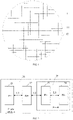
- FIG. 1 is a schematic diagram of an application scenario of an integrated circuit latch-up test structure according to the present disclosure.
- the application scenario of the integrated circuit latch-up test structure provided by the present disclosure involves a wafer 1 and the integrated circuit latch-up test structure, a plurality of bare dies 12 and scribe lines 11 are formed after the wafer 1 is cut, wherein the integrated circuit latch-up test structure may be located on the wafer 1.
- the integrated circuit latch-up test structure may be located in the scribe lines 11 or the bare dies 12.
- the integrated circuit on the bare dies 12 has the same as an equivalent circuit corresponding to the integrated circuit latch-up test structure.
- the electrical parameters include a trigger voltage for triggering the latch-up effect, a holding voltage for holding the latch-up effect, a trigger current for triggering the latch-up effect, and a holding current for holding the latch-up effect.
- the trigger voltage is greater, the latch-up is less likely to cause; and the holding voltage is greater, the latch-up effect is less likely to hold.
- Supposing a normal working voltage is 1.1V
- a risk of triggering the latch-up effect is greater if the trigger voltage is 1.2V.
- the risk of triggering the latch-up effect is smaller if the trigger voltage is 2V.
- the holding voltage has the same principle. It is to be noted that the holding voltage generally is smaller than the trigger voltage.
- the trigger voltage is 2V
- the holding voltage may be 1.8V
- the integrated circuit latch-up test structure includes a first P-type heavily doped region, a first N-type heavily doped region, a second P-type heavily doped region, and a second N-type heavily doped region.
- a first distance is provided between the first P-type heavily doped region and the first N-type heavily doped region
- a second distance is provided between the first N-type heavily doped region and the second P-type heavily doped region
- a third distance is provided between the second P-type heavily doped region and the second N-type heavily doped region.
- the first P-type heavily doped regions, the first N-type heavily doped regions, the second P-type heavily doped regions and the second N-type heavily doped regions are arranged on different locations.
- the first distance, the second distance and the third distance are related to the trigger voltage for triggering the latch-up effect, the holding voltage for holding the latch-up effect, the trigger current for triggering the latch-up effect, and the holding current for holding the latch-up effect.
- the electrical parameters i.e., the trigger voltage for triggering the latch-up effect, the holding voltage for holding the latch-up effect, the trigger current for triggering the latch-up effect, and the holding current for holding the latch-up effect
- the latch-up effect of the integrated circuit corresponding to the integrated circuit latch-up test structure may be tested by adjusting at least one of the first distance, the second distance, and the third distance.
- the first distance, the second distance and the third distance in the integrated circuit on the dare dies 12 may be set by the electrical parameters of the latch-up effect and the first distance, the second distance, and the third distance.
- occurrence of the latch-up effect can be prevented in a working process of the integrated circuit on the dare dies 12, and the chip is prevented from being burned out due to the latch-up effect, the reliability of the chip is improved.
- various corresponding integrated circuit latch-up test structures may also be designed by changing magnitudes of the first distance, the second distance, and the third distance.
- the electrical parameters (also referred to as latch-up characteristics) of the latch-up effect of this integrated circuit latch-up test structure may be evaluated based on a transmission line pulse (TLP) test.
- TLP transmission line pulse
- FIGS. 2 to 22 illustrate seven types of integrated circuit latch-up test structures in total.
- the first P-type heavily doped regions, the first N-type heavily doped regions, the second P-type heavily doped regions and the second N-type heavily doped regions are arranged on different locations. It is to be noted that in FIGS. 2 to 22 , the P-type heavily doped region is referred to as P+, and the N-type heavily doped region is referred to as N+.
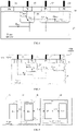
- FIG. 2 is a top view of an integrated circuit latch-up test structure according to an embodiment of the present disclosure
- FIG. 3 is a sectional view of an integrated circuit latch-up test structure according to an embodiment of the present disclosure.
- the integrated circuit latch-up test structure of this embodiment may include: a first P-type heavily doped region 21, a first N-type heavily doped region 22, a second P-type heavily doped region 23, and a second N-type heavily doped region 24.
- the first P-type heavily doped region 21 and the first N-type heavily doped region 22 are both located on a P-type substrate, the second P-type heavily doped region 23 and the second N-type heavily doped region 24 are both located in an N-well 25, and the N-well 25 is located on the P-type substrate 26.
- a first distance L1 is provided between the first P-type heavily doped region 21 and the first N-type heavily doped region 22, a second distance L2 is provided between the first N-type heavily doped region 22 and the second P-type heavily doped region 23, and a third distance L3 is provided between the second P-type heavily doped region 23 and the second N-type heavily doped region 24.
- the test structure is configured to test electrical parameters of a latch-up effect of an integrated circuit corresponding to the test structure by adjusting at least one of the first distance L1, the second distance L2, and the third distance L3.
- the N-well 25, the P-type substrate 26 and the first N-type heavily doped region 22 constitute a first parasitic NPN transistor T1.
- the second P-type heavily doped region 23, the N-well 25 and the P-type substrate 26 constitute a first parasitic PNP transistor T2.
- the P-type substrate 26 has a first parasitic resistor RPW, wherein a first terminal of the first parasitic resistor RPW is connected to the first P-type heavily doped region, and a second terminal of the first parasitic resistor RPW is connected to a base of the first parasitic NPN transistor T1.
- the N-well 25 has a second parasitic resistor RNW, wherein a first terminal of the second parasitic resistor RNW is connected to the second N-type heavily doped region 24, and a second terminal of the second parasitic resistor RNW is connected to a base of the first parasitic PNP transistor T2.
- FIG. 4 is a schematic connection diagram of the integrated circuit latch-up test structures as shown in FIG. 2 and FIG. 3 when in test.
- the first P-type heavily doped region 21 and the first N-type heavily doped region 22 are both connected to a ground terminal VSS
- the second P-type heavily doped region 23 and the second N-type heavily doped region 24 are both connected to a power supply terminal VDD.
- a voltage applied to the power supply terminal VDD is gradually increased from 0V, for example, gradually increased from 0V to 5V.
- a current between the power supply terminal VDD and the ground terminal VSS is monitored.
- the first distance L1, the second distance L2 and the third distance L3 are related to the trigger voltage for triggering the latch-up effect, the holding voltage for holding the latch-up effect, the trigger current for triggering the latch-up effect, and the holding current for holding the latch-up effect.
- a corresponding relationship table between the first distance L1, the second distance L2 and the third distance L3 and the trigger voltage for triggering the latch-up effect, the holding voltage for holding the latch-up effect, the trigger current for triggering the latch-up effect, and the holding current for holding the latch-up effect may be measured.
- the table can be used as a basis for designing an integrated circuit corresponding to the integrated circuit latch-up test structure as shown in FIG. 2 and FIG. 3 , to avoid the latch-up effect in a working process of the integrated circuit corresponding to the integrated circuit latch-up test structure.
- the corresponding table can be in the form shown in Table 1 below.
- the first group distance (including the first distance L1, the second distance L2, and the third distance L3) The trigger voltage for triggering the latch-up effect, the holding voltage for holding the latch-up effect, the trigger current for triggering the latch-up effect, and the holding current for holding the latch-up effect
- the second group distance (including the first distance L1, the second distance L2, and the third distance L3) The trigger voltage for triggering the latch-up effect, the holding voltage for holding the latch-up effect, the trigger current for triggering the latch-up effect, and the holding current for holding the latch-up effect
- the third group distance (including the first distance L1, the second distance L2, and the third distance L3) The trigger voltage for triggering the latch-up effect, the holding voltage for holding the latch-up effect, the trigger current for triggering the latch-up effect, and the holding current for holding the latch-up effect
- the Nth group of distance (including the first distance L1, the second distance L2, and the third distance L3) The trigger voltage for triggering the latch-up effect, the holding voltage for holding the latch-
- T2 is a vertical PNP transistor
- a base is an N-well
- a gain from the base to a collector may be up to dozens of times.
- T1 is a side NPN transistor
- a base is a P-type substrate
- a gain from the base to a collector may be up to dozens of times.
- RNW is a parasitic resistor of the N-well
- RPW is a parasitic resistor of the P-type substrate.
- the above four components T1, T2, RNW and RPW constitute a thyristor circuit.
- the two transistors When there is no external interference or triggering, the two transistors are in an off state.
- a collector current has a C-B reverse leakage current, and a current gain is very small, which will not cause a latch-up.
- the collector current of one of the two transistors increases abruptly to a certain value due to external interferences, it will be fed back to the other transistor, such that the two transistors are turned on due to triggering (generally, PNP is easier to trigger), and thus a low-impedance path is formed between the power supply terminal VDD and the ground terminal VSS.
- current leakage i.e., a lock state
- between the power supply terminal VDD and the ground terminal VSS may still exist due to positive feedback formed between the two triodes. This results in the latch-up effect.
- This embodiment provides an integrated circuit latch-up test structure.
- electrical parameters of the latch-up effect of the integrated circuit corresponding to the integrated circuit latch-up test structure may be tested by adjusting at least one of the first distance, the second distance, and the third distance.
- the first distance, the second distance and the third distance in the integrated circuit corresponding to the integrated circuit latch-up test structure may be set by means of the electrical parameters of the latch-up effect and the first distance, the second distance, and the third distance.
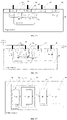
- FIG. 5 is a top view of an integrated circuit latch-up test structure according to an embodiment of the present disclosure
- FIG. 6 is a sectional view of an integrated circuit latch-up test structure according to an embodiment of the present disclosure.
- the integrated circuit latch-up test structure of this embodiment may include: a first P-type heavily doped region 31, a first N-type heavily doped region 32, a second P-type heavily doped region 33, and a second N-type heavily doped region 34.
- the first P-type heavily doped region 31 is located on a P-type substrate 37
- the first N-type heavily doped region 32 is located in a first N-well 35
- the second P-type heavily doped region and the second N-type heavily doped region 34 both are located in a second N-well 36
- the first N-well 35 and the second N-well 36 both are located on the P-type substrate 37.
- the first distance L1 is provided between the first P-type heavily doped region 31 and the first N-type heavily doped region 32
- the second distance L2 is provided between the first N-type heavily doped region 32 and the second P-type heavily doped region 33
- the third distance L3 is provided between the second P-type heavily doped region 33 and the second N-type heavily doped region 34.
- the test structure is configured to test the electrical parameters of the latch-up effect of the integrated circuit corresponding to the test structure by adjusting at least one of the first distance L1, the second distance L2, and the third distance L3.
- the second N-well 36, the P-type substrate 37 and the first N-type heavily doped region 32 constitute the first parasitic NPN transistor T1.
- the second P-type heavily doped region 33, the second N-well 36 and the P-type substrate 37 constitute the first parasitic PNP transistor T2.
- the P-type substrate 37 has a first parasitic resistor RPW, wherein a first terminal of the first parasitic resistor RPW is connected to the first P-type heavily doped region 31, and a second terminal of the first parasitic resistor RPW is connected to a base of the first parasitic NPN transistor T1.
- the second N-well 36 has a second parasitic resistor RNW, wherein a first terminal of the second parasitic resistor RNW is connected to the second N-type heavily doped region 34, and a second terminal of the second parasitic resistor RNW is connected to a base of the first parasitic PNP transistor T2.
- FIG. 7 is a schematic connection diagram of the integrated circuit latch-up test structures as shown in FIG. 5 and FIG. 6 when in test.
- the first P-type heavily doped region 31 and the first N-type heavily doped region 32 are both connected to a ground terminal VSS
- the second P-type heavily doped region 33 and the second N-type heavily doped region 34 are both connected to a power supply terminal VDD.
- a voltage applied to the power supply terminal VDD is gradually increased from 0V, for example, gradually increased from 0V to 5V.
- a current between the power supply terminal VDD and the ground terminal VSS is monitored.
- the first distance L1, the second distance L2 and the third distance L3 are related to the trigger voltage for triggering the latch-up effect, the holding voltage for holding the latch-up effect, the trigger current for triggering the latch-up effect, and the holding current for holding the latch-up effect.
- a corresponding relationship table between the first distance L1, the second distance L2 and the third distance L3 and the trigger voltage for triggering the latch-up effect, the holding voltage for holding the latch-up effect, the trigger current for triggering the latch-up effect, and the holding current for holding the latch-up effect may be measured.
- the table can be used as a basis for designing an integrated circuit corresponding to the integrated circuit latch-up test structure as shown in FIG. 5 and FIG. 6 , to avoid the latch-up effect in a working process of the integrated circuit corresponding to the integrated circuit latch-up test structure.
- the corresponding table can be in the form of shown in Table 1 above.
- T2 is a vertical PNP transistor
- a base is an N-well
- a gain from the base to a collector may be up to hundreds of times.
- T1 is a side NPN transistor
- a base is a P-type substrate
- a gain from the base to a collector may be up to dozens of times.
- RNW is a parasitic resistor of the second N-well
- RPW is a parasitic resistor of the P-type substrate.
- the above four components T1, T2, RNW and RPW constitute a thyristor circuit.
- the two transistors When there is no external interference or triggering, the two transistors are in an off state.
- a collector current has a C-B reverse leakage current, and a current gain is very small, which will not cause a latch-up.
- the collector current of one of the two transistors increases abruptly to a certain value due to external interferences, it will be fed back to the other transistor, such that the two transistors are turned on due to triggering (generally, PNP is easier to trigger), and thus a low-impedance path is formed between the power supply terminal VDD and the ground terminal VSS.
- current leakage i.e., a lock state
- between the power supply terminal VDD and the ground terminal VSS may still exist due to positive feedback formed between the two triodes. This results in the latch-up effect.
- This embodiment provides an integrated circuit latch-up test structure.
- electrical parameters of the latch-up effect of an integrated circuit corresponding to the integrated circuit latch-up test structure may be tested by adjusting at least one of the first distance, the second distance, and the third distance.
- the first distance, the second distance and the third distance in the integrated circuit corresponding to the integrated circuit latch-up test structure may be set by means of the electrical parameters of the latch-up effect and the first distance, the second distance, and the third distance.
- FIG. 8 is a top view of an integrated circuit latch-up test structure according to an embodiment of the present disclosure
- FIG. 9 is a sectional view of an integrated circuit latch-up test structure according to an embodiment of the present disclosure.
- the integrated circuit latch-up test structure of this embodiment may include: a first P-type heavily doped region 41, a first N-type heavily doped region 42, a second P-type heavily doped region 43, and a second N-type heavily doped region 44.
- the first P-type heavily doped region 41 is located on a P-type substrate 45
- the first N-type heavily doped region 42 is located in a deep N-well 46
- the deep N-well 46 is located in a first N-well 47
- the second P-type heavily doped region 43 and the second N-type heavily doped region 44 both are located in a second N-well 48
- the first N-well 47 and the second N-well 48 both are located on the P-type substrate 45.
- the first distance L1 is provided between the first P-type heavily doped region 41 and the first N-type heavily doped region 42
- the second distance L2 is provided between the first N-type heavily doped region 42 and the second P-type heavily doped region 43
- the third distance L3 is provided between the second P-type heavily doped region 43 and the second N-type heavily doped region 44.
- the test structure is configured to test the electrical parameters of the latch-up effect of the integrated circuit corresponding to the test structure by adjusting at least one of the first distance L1, the second distance L2, and the third distance L3.
- the second N-well 48, the P-type substrate 45 and the deep N-well 46 constitute the first parasitic NPN transistor T1.
- the second P-type heavily doped region 43, the second N-well 48 and the P-type substrate 45 constitute the first parasitic PNP transistor T2.
- the P-type substrate 45 has a first parasitic resistor RPW, wherein a first terminal of the first parasitic resistor RPW is connected to the first P-type heavily doped region 41, and a second terminal of the first parasitic resistor RPW is connected to an emitter of the first parasitic NPN transistor T1.
- the second N-well 48 has a second parasitic resistor RNW, wherein a first terminal of the second parasitic resistor RNW is connected to the second N-type heavily doped region 44, and a second terminal of the second parasitic resistor RNW is connected to a base of the first parasitic PNP transistor T2.
- FIG. 10 is a schematic connection diagram of the integrated circuit latch-up test structures as shown in FIG. 8 and FIG. 9 when in test.
- the first P-type heavily doped region 41 and the first N-type heavily doped region 42 are both connected to a ground terminal VSS
- the second P-type heavily doped region 43 and the second N-type heavily doped region 44 are both connected to a power supply terminal VDD.
- a voltage applied to the power supply terminal VDD is gradually increased from 0V, for example, gradually increased from 0V to 5V.
- a current between the power supply terminal VDD and the ground terminal VSS is monitored.
- the first distance L1, the second distance L2 and the third distance L3 are related to the trigger voltage for triggering the latch-up effect, the holding voltage for holding the latch-up effect, the trigger current for triggering the latch-up effect, and the holding current for holding the latch-up effect.
- a corresponding relationship table between the first distance L1, the second distance L2 and the third distance L3 and the trigger voltage for triggering the latch-up effect, the holding voltage for holding the latch-up effect, the trigger current for triggering the latch-up effect, and the holding current for holding the latch-up effect may be measured.
- the table can be used as a basis for designing an integrated circuit corresponding to the integrated circuit latch-up test structure as shown in FIG. 8 and FIG. 9 , avoid the latch-up effect in a working process of the integrated circuit corresponding to the integrated circuit latch-up test structure.
- the corresponding table can be in the form of shown in Table 1 above.
- T2 is a vertical PNP transistor
- a base is an N-well
- a gain from the base to a collector may be up to hundreds of times.
- T1 is a side NPN transistor
- a base is a P-type substrate
- a gain from the base to a collector may be up to dozens of times.
- RNW is a parasitic resistor of the second N-well
- RPW is a parasitic resistor of the P-type substrate.
- the above four components T1, T2, RNW and RPW constitute a thyristor circuit.
- the two transistors When there is no external interference or triggering, the two transistors are in an off state.
- a collector current has a C-B reverse leakage current, and a current gain is very small, which will not cause a latch-up.
- the collector current of one of the two transistors increases abruptly to a certain value due to external interferences, will be fed back to the other transistor, such that the two transistors are turned on due to triggering (generally, PNP is easier to trigger), and thus a low-impedance path is formed between the power supply terminal VDD and the ground terminal VSS.
- current leakage i.e., a lock state
- between the power supply terminal VDD and the ground terminal VSS may still exist due to positive feedback formed between the two triodes. This results in the latch-up effect.
- This embodiment provides an integrated circuit latch-up test structure.
- electrical parameters of the latch-up effect of an integrated circuit corresponding to the integrated circuit latch-up test structure may be tested by adjusting at least one of the first distance, the second distance, and the third distance.
- the first distance, the second distance and the third distance in the integrated circuit corresponding to the integrated circuit latch-up test structure may be set by means of the electrical parameters of the latch-up effect and the first distance, the second distance, and the third distance.
- FIG. 11 is a top view of an integrated circuit latch-up test structure according to an embodiment of the present disclosure
- FIG. 12 is a sectional view of an integrated circuit latch-up test structure according to an embodiment of the present disclosure.
- the integrated circuit latch-up test structure of this embodiment may include: a first N-type heavily doped region 51, a first P-type heavily doped region 52, a second N-type heavily doped region 53, and a second P-type heavily doped region 54.
- the first N-type heavily doped region 51 and the first P-type heavily doped region 52 are both located in a deep N-well 55, the deep N-well 55 is located in an N-well 56, and the N-well 56 is located on a P-type substrate 57.
- the second N-type heavily doped region 53 and the second P-type heavily doped region 54 are both located in a P-well 58, and the P-well 58 is located in a deep N-well 55.
- the first distance L1 is provided between the first N-type heavily doped region 51 and the first P-type heavily doped region 52
- the second distance L2 is provided between the first P-type heavily doped region 52 and the second N-type heavily doped region 53
- the third distance L3 is provided between the second N-type heavily doped region 53 and the second P-type heavily doped region 54.
- the test structure is configured to test the electrical parameters of the latch-up effect of the integrated circuit corresponding to the test structure by adjusting at least one of the first distance L1, the second distance L2, and the third distance L3.
- the first P-type heavily doped region 52, the deep N-well 55 and the second P-type heavily doped region 54 constitute the first parasitic PNP transistor T1.
- the first N-type heavily doped region 51, the P-type substrate 57 and the deep N-well 55 constitute the first parasitic NPN transistor T2.
- the deep N-well 55 has a first parasitic resistor RDNW, wherein a first terminal of the first parasitic resistor RDNW is connected to the first N-type heavily doped region, and a second terminal of the first parasitic resistor RDNW is connected to a base of the first parasitic PNP transistor T1.
- the P-well 58 has a second parasitic resistor RPW, wherein a first terminal of the second parasitic resistor RPW is connected to the second P-type heavily doped region 54, and a second terminal of the second parasitic resistor RPW is connected to a base of the first parasitic NPN transistor T2 and a collector of the first parasitic PNP transistor T1.
- FIG. 13 is a schematic connection diagram of the integrated circuit latch-up test structures as shown in FIG. 11 and FIG. 12 when in test.
- the first P-type heavily doped region 52 and the first N-type heavily doped region 51 are both connected to a power supply terminal VDD
- the second P-type heavily doped region 43 and the second N-type heavily doped region 44 are both connected to a ground terminal VSS.
- a voltage applied to the power supply terminal VDD is gradually increased from 0V, for example, gradually increased from 0V to 5V.
- a current between the power supply terminal VDD and the ground terminal VSS is monitored.
- the first distance L1, the second distance L2 and the third distance L3 are related to the trigger voltage for triggering the latch-up effect, the holding voltage for holding the latch-up effect, the trigger current for triggering the latch-up effect, and the holding current for holding the latch-up effect.
- a corresponding relationship table between the first distance L1, the second distance L2 and the third distance L3 and the trigger voltage for triggering the latch-up effect, the holding voltage for holding the latch-up effect, the trigger current for triggering the latch-up effect, and the holding current for holding the latch-up effect may be measured.
- the table can be used as a basis for designing an integrated circuit corresponding to the integrated circuit latch-up test structure as shown in FIG. 11 and FIG. 12 , to avoid the latch-up effect in a working process of the integrated circuit corresponding to the integrated circuit latch-up test structure.
- the relationship table can be in the form of shown in Table 1 above.
- T1 is a vertical PNP transistor
- a base is an N-well
- a gain from the base to a collector may be up to hundreds of times.
- T2 is a side NPN transistor
- a base is a P-type substrate
- a gain from the base to a collector may be up to dozens of times.
- RDNW is a parasitic resistor of the deep N-well
- RPW is a parasitic resistor of the P-well.
- the above four components T1, T2, RDNW and RPW constitute a thyristor circuit.
- the two transistors When there is no external interference or triggering, the two transistors are in an off state.
- a collector current has a C-B reverse leakage current, and a current gain is very small, which will not cause a latch-up.
- the collector current of one of the two transistors increases abruptly to a certain value due to external interferences, it will be fed back to the other transistor, such that the two transistors are turned on due to triggering (generally, PNP is easier to trigger), and thus a low-impedance path is formed between the power supply terminal VDD and the ground terminal VSS.
- current leakage i.e., a lock state
- between the power supply terminal VDD and the ground terminal VSS may still exist due to positive feedback formed between the two triodes. This results in the latch-up effect.
- This embodiment provides an integrated circuit latch-up test structure.
- electrical parameters of the latch-up effect of an integrated circuit corresponding to the integrated circuit latch-up test structure may be tested by adjusting at least one of the first distance, the second distance, and the third distance.
- the first distance, the second distance and the third distance in the integrated circuit corresponding to the integrated circuit latch-up test structure may be set by means of the electrical parameters of the latch-up effect and the first distance, the second distance, and the third distance.
- FIG. 14 is a top view of an integrated circuit latch-up test structure according to an embodiment of the present disclosure
- FIG. 15 is a sectional view of an integrated circuit latch-up test structure according to an embodiment of the present disclosure.
- the integrated circuit latch-up test structure of this embodiment may include: a first N-type heavily doped region 61, a first P-type heavily doped region 62, a second N-type heavily doped region 63, and a second P-type heavily doped region 64.
- the first N-type heavily doped region 61 is located in an N-well 65, and the N-well 65 is located on a P-type substrate 66.
- the first P-type heavily doped region 62 is located in a P-well 67, the P-well 67 is located in a deep N-well 68, and the deep N-well 68 is located in the N-well 65.
- the second N-type heavily doped region 63 and the second P-type heavily doped region 64 both are located on the P-type substrate 66.
- the first distance L1 is provided between the first N-type heavily doped region 61 and the first P-type heavily doped region 62
- the second distance L2 is provided between the first P-type heavily doped region 62 and the second N-type heavily doped region 63
- the third distance L3 is provided between the second N-type heavily doped region 63 and the second P-type heavily doped region 64.
- the test structure is configured to test the electrical parameters of the latch-up effect of the integrated circuit corresponding to the test structure by adjusting at least one of the first distance L1, the second distance L2, and the third distance L3.
- the P-well 67, the deep N-well 68 and the P-type substrate 66 constitute the first parasitic PNP transistor T1.
- the deep N-well 68, the P-type substrate 66 and the second N-type heavily doped region 63 constitute the first parasitic NPN transistor T2.
- the deep N-well 68 has a first parasitic resistor RDNW, wherein a first terminal of the first parasitic resistor RDNW is connected to the first N-type heavily doped region 61, and a second terminal of the first parasitic resistor RDNW is connected to a base of the first parasitic PNP transistor T1.
- the P-type substrate 66 has a second parasitic resistor RPW, wherein a first terminal of the second parasitic resistor RPW is connected to the second P-type heavily doped region 64, and a second terminal of the second parasitic resistor RPW is connected to a base of the first parasitic NPN transistor T2 and a collector of the first parasitic PNP transistor T1.
- FIG. 16 is a schematic connection diagram of the integrated circuit latch-up test structures as shown in FIG. 14 and FIG. 15 when in test.
- the first P-type heavily doped region 62 and the first N-type heavily doped region 61 are both connected to a power supply terminal VDD
- the second P-type heavily doped region 64 and the second N-type heavily doped region 63 are both connected to a ground terminal VSS.
- a voltage applied to the power supply terminal VDD is gradually increased from 0V, for example, gradually increased from 0V to 5V.
- a current between the power supply terminal VDD and the ground terminal VSS is monitored.
- the first distance L1, the second distance L2 and the third distance L3 are related to the trigger voltage for triggering the latch-up effect, the holding voltage for holding the latch-up effect, the trigger current for triggering the latch-up effect, and the holding current for holding the latch-up effect.
- a corresponding relationship table between the first distance L1, the second distance L2 and the third distance L3 and the trigger voltage for triggering the latch-up effect, the holding voltage for holding the latch-up effect, the trigger current for triggering the latch-up effect, and the holding current for holding the latch-up effect may be measured.
- the table can be used as a basis for designing an integrated circuit corresponding to the integrated circuit latch-up test structure as shown in FIG. 14 and FIG. 15 , to avoid the latch-up effect in a working process of the integrated circuit corresponding to the integrated circuit latch-up test structure.
- the relationship table can be in the form of shown in Table 1 above.
- T1 is a vertical PNP transistor
- a base is an N-well
- a gain from the base to a collector may be up to hundreds of times.
- T2 is a side NPN transistor
- a base is a P-type substrate
- a gain from the base to a collector may be up to dozens of times.
- RDNW is a parasitic resistor of the deep N-well
- RPW is a parasitic resistor of the P-type substrate.
- the above four components T1, T2, RDNW and RPW constitute a thyristor circuit.
- the two transistors When there is no external interference or triggering, the two transistors are in an off state.
- a collector current has a C-B reverse leakage current, and a current gain is very small, which will not cause a latch-up.
- the collector current of one of the two transistors increases abruptly to a certain value due to external interferences, it will be fed back to the other transistor, such that the two transistors are turned on due to triggering (generally, PNP is easier to trigger), and thus a low-impedance path is formed between the power supply terminal VDD and the ground terminal VSS.
- current leakage i.e., a lock state
- between the power supply terminal VDD and the ground terminal VSS may still exist due to positive feedback formed between the two triodes. This results in the latch-up effect.
- This embodiment provides an integrated circuit latch-up test structure.
- electrical parameters of the latch-up effect of an integrated circuit corresponding to the integrated circuit latch-up test structure may be tested by adjusting at least one of the first distance, the second distance, and the third distance.
- the first distance, the second distance and the third distance in the integrated circuit corresponding to the integrated circuit latch-up test structure may be set by means of the electrical parameters of the latch-up effect and the first distance, the second distance, and the third distance.
- FIG. 17 is a top view of an integrated circuit latch-up test structure according to an embodiment of the present disclosure
- FIG. 18 is a sectional view of an integrated circuit latch-up test structure according to an embodiment of the present disclosure.
- the integrated circuit latch-up test structure of this embodiment may include: a first N-type heavily doped region 71, a first P-type heavily doped region 72, a second N-type heavily doped region 73, and a second P-type heavily doped region 74.
- the first N-type heavily doped region 71 is located in a first N-well 75, and the first N-well 75 is located on a P-type substrate 76.
- the first P-type heavily doped region 72 is located in a P-well 77, the P-well 77 is located in a deep N-well 78, and the deep N-well 78 is located in the first N-well 75.
- the second N-type heavily doped region 73 is located in a second N-well 79, and the second N-well 79 is located on a P-type substrate 76.
- the second P-type heavily doped region 74 is located on the P-type substrate 76.
- the first distance L1 is provided between the first N-type heavily doped region 71 and the first P-type heavily doped region 72
- the second distance L2 is provided between the first P-type heavily doped region 72 and the second N-type heavily doped region 73
- the third distance L3 is provided between the second N-type heavily doped region 73 and the second P-type heavily doped region 74.
- the test structure is configured to test the electrical parameters of the latch-up effect of the integrated circuit corresponding to the test structure by adjusting at least one of the first distance L1, the second distance L2, and the third distance L3.
- the P-well 77, the deep N-well 78 and the P-type substrate 76 constitute the first parasitic PNP transistor T1.
- the deep N-well 78, the P-type substrate 76 and the second N-well 79 constitute the first parasitic NPN transistor T2.
- the deep N-well 78 has a first parasitic resistor RDNW, wherein a first terminal of the first parasitic resistor RDNW is connected to the first N-type heavily doped region 71, and a second terminal of the first parasitic resistor RDNW is connected to a base of the first parasitic PNP transistor T1.
- the P-type substrate 76 has a second parasitic resistor RPW, wherein a first terminal of the second parasitic resistor RPW is connected to the second P-type heavily doped region 74, and a second terminal of the second parasitic resistor RPW is connected to a base of the first parasitic NPN transistor T2 and a collector of the first parasitic PNP transistor T1.
- FIG. 19 is a schematic connection diagram of the integrated circuit latch-up test structures as shown in FIG. 17 and FIG. 18 when in test.
- the first P-type heavily doped region 72 and the first N-type heavily doped region 71 are both connected to a power supply terminal VDD
- the second P-type heavily doped region 74 and the second N-type heavily doped region 73 are both connected to a ground terminal VSS.
- a voltage applied to the power supply terminal VDD is gradually increased from 0V, for example, gradually increased from 0V to 5V.
- a current between the power supply terminal VDD and the ground terminal VSS is monitored.
- the first distance L1, the second distance L2 and the third distance L3 are related to the trigger voltage for triggering the latch-up effect, the holding voltage for holding the latch-up effect, the trigger current for triggering the latch-up effect, and the holding current for holding the latch-up effect.
- a corresponding relationship table between the first distance L1, the second distance L2 and the third distance L3 and the trigger voltage for triggering the latch-up effect, the holding voltage for holding the latch-up effect, the trigger current for triggering the latch-up effect, and the holding current for holding the latch-up effect may be measured.
- the table can be used as a basis for designing an integrated circuit corresponding to the integrated circuit latch-up test structure as shown in FIG. 17 and FIG. 18 , to avoid the latch-up effect in a working process of the integrated circuit corresponding to the integrated circuit latch-up test structure.
- the relationship table can be in the form of shown in Table 1 above.
- T1 is a vertical PNP transistor
- a base is an N-well
- a gain from the base to a collector may be up to hundreds of times.
- T2 is a side NPN transistor
- a base is a P-type substrate
- a gain from the base to a collector may be up to dozens of times.
- RDNW is a parasitic resistor of the deep N-well
- RPW is a parasitic resistor of the P-type substrate.
- the above four components T1, T2, RDNW and RPW constitute a thyristor circuit.
- the two transistors When there is no external interference or triggering, the two transistors are in an off state.
- a collector current has a C-B reverse leakage current, and a current gain is very small, which will not cause a latch-up.
- the collector current of one of the two transistors increases abruptly to a certain value due to external interferences, it will be fed back to the other transistor, such that the two transistors are turned on due to triggering (generally, PNP is easier to trigger), and thus a low-impedance path is formed between the power supply terminal VDD and the ground terminal VSS.
- current leakage i.e., a lock state
- between the power supply terminal VDD and the ground terminal VSS may still exist due to positive feedback formed between the two triodes. This results in the latch-up effect.
- This embodiment provides an integrated circuit latch-up test structure.
- electrical parameters of the latch-up effect of an integrated circuit corresponding to the integrated circuit latch-up test structure may be tested by adjusting at least one of the first distance, the second distance, and the third distance.
- the first distance, the second distance and the third distance in the integrated circuit corresponding to the integrated circuit latch-up test structure may be set by means of the electrical parameters of the latch-up effect and the first distance, the second distance, and the third distance.
- FIG. 20 is a top view of an integrated circuit latch-up test structure according to an embodiment of the present disclosure
- FIG. 21 is a sectional view of an integrated circuit latch-up test structure according to an embodiment of the present disclosure.
- the integrated circuit latch-up test structure of this embodiment may include: a first N-type heavily doped region 81, a first P-type heavily doped region 82, a second N-type heavily doped region 83, and a second P-type heavily doped region 84.
- the first N-type heavily doped region 81 is located in a first N-well 85, and the first N-well 85 is located on a P-type substrate 86.
- the first P-type heavily doped region 82 is located in a P-well 87, the P-well 87 is located in a first deep N-well 88, and the first deep N-well 88 is located in the first N-well 85.
- the second N-type heavily doped region 83 is located in a second deep N-well 89, the second deep N-well 89 is located in a second N-well 90, and the second N-well 90 is located on the P-type substrate 86.
- the second P-type heavily doped region 84 is located on the P-type substrate 86.
- the first distance L1 is provided between the first N-type heavily doped region 81 and the first P-type heavily doped region 82
- the second distance L2 is provided between the first P-type heavily doped region 82 and the second N-type heavily doped region 83
- the third distance L3 is provided between the second N-type heavily doped region 83 and the second P-type heavily doped region 84.
- the test structure is configured to test the electrical parameters of the latch-up effect of the integrated circuit corresponding to the test structure by adjusting at least one of the first distance L1, the second distance L2, and the third distance L3.
- the P-well 87, the first deep N-well 88 and the P-type substrate 86 constitute the first parasitic PNP transistor T1.
- the first deep N-well 88, the P-type substrate 86 and the second deep N-well 89 constitute the first parasitic NPN transistor T2.
- the deep N-well 88 has a first parasitic resistor RDNW, wherein a first terminal of the first parasitic resistor RDNW is connected to the first N-type heavily doped region 81, and a second terminal of the first parasitic resistor RDNW is connected to a base of the first parasitic PNP transistor T1.
- the P-type substrate 86 has a second parasitic resistor RPW, wherein a first terminal of the second parasitic resistor RPW is connected to the second P-type heavily doped region 84, and a second terminal of the second parasitic resistor RPW is connected to a base of the first parasitic NPN transistor T2 and a collector of the first parasitic PNP transistor T1.
- FIG. 22 is a schematic connection diagram of the integrated circuit latch-up test structures as shown in FIG. 20 and FIG. 21 when in test.
- the first P-type heavily doped region 82 and the first N-type heavily doped region 81 are both connected to a power supply terminal VDD
- the second P-type heavily doped region 84 and the second N-type heavily doped region 83 are both connected to a ground terminal VSS.
- a voltage applied to the power supply terminal VDD is gradually increased from 0V, for example, gradually increased from 0V to 5V.
- a current between the power supply terminal VDD and the ground terminal VSS is monitored.
- the first distance L1, the second distance L2 and the third distance L3 are related to the trigger voltage for triggering the latch-up effect, the holding voltage for holding the latch-up effect, the trigger current for triggering the latch-up effect, and the holding current for holding the latch-up effect.
- a corresponding relationship table between the first distance L1, the second distance L2 and the third distance L3 and the trigger voltage for triggering the latch-up effect, the holding voltage for holding the latch-up effect, the trigger current for triggering the latch-up effect, and the holding current for holding the latch-up effect may be measured.
- the table can be used as a basis for designing an integrated circuit corresponding to the integrated circuit latch-up test structure as shown in FIG. 20 and FIG. 21 , to avoid the latch-up effect in a working process of the integrated circuit corresponding to the integrated circuit latch-up test structure.
- the relationship table can be in the form of shown in Table 1 above.
- T1 is a vertical PNP transistor
- a base is an N-well
- a gain from the base to a collector may be up to hundreds of times.
- T2 is a side NPN transistor
- a base is a P-type substrate
- a gain from the base to a collector may be up to dozens of times.
- RDNW is a parasitic resistor of the first deep N-well
- RPW is a parasitic resistor of the P-type substrate.
- the above four components T1, T2, RDNW and RPW constitute a thyristor circuit.
- the two transistors When there is no external interference or triggering, the two transistors are in an off state.
- a collector current has a C-B reverse leakage current, and a current gain is very small, which will not cause a latch-up.
- the collector current of one of the two transistors increases abruptly to a certain value due to external interferences, it will be fed back to the other transistor, such that the two transistors are turned on due to triggering (generally, PNP is easier to trigger), and thus a low-impedance path is formed between the power supply terminal VDD and the ground terminal VSS.
- current leakage i.e., a lock state
- between the power supply terminal VDD and the ground terminal VSS may still exist due to positive feedback formed between the two triodes. This results in the latch-up effect.
- This embodiment provides an integrated circuit latch-up test structure.
- electrical parameters of the latch-up effect of an integrated circuit corresponding to the integrated circuit latch-up test structure may be tested by adjusting at least one of the first distance, the second distance, and the third distance.
- the first distance, the second distance and the third distance in the integrated circuit corresponding to the integrated circuit latch-up test structure may be set by means of the electrical parameters of the latch-up effect and the first distance, the second distance, and the third distance.
Landscapes
- Engineering & Computer Science (AREA)
- Computer Hardware Design (AREA)
- Microelectronics & Electronic Packaging (AREA)
- General Engineering & Computer Science (AREA)
- Physics & Mathematics (AREA)
- General Physics & Mathematics (AREA)
- Metal-Oxide And Bipolar Metal-Oxide Semiconductor Integrated Circuits (AREA)
- Semiconductor Integrated Circuits (AREA)
Abstract
Description
- This application claims priority to
Chinese Patent Application No. 202110149970.8 titled "INTEGRATED CIRCUIT LATCH-UP TEST STRUCTURE" and filed to the State Intellectual Property Office on February 03, 2021 - The present disclosure relates to the technical field of integrated circuits, and in particular to an integrated circuit latch-up test structure.
- As a parasitic effect unique to Complementary Metal-Oxide-Semiconductor Transistor (CMOS) technologies, a latch-up effect may seriously cause failure of circuits and even burn out chips. The latch-up effect is produced by an n-p-n-p structure comprising an active region of an N-channel metal oxide semiconductor (NMOS), a P-type substrate, an N-well and a P-channel metal oxide semiconductor (PMOS). When one of triodes is positively biased, a positive feedback may be constituted, and latch-up may be formed. As an invisible destructive force, static electricity may have a negative effect on electronic components. Either of the static electricity and related voltage transients may cause the latch-up effect, which is one of primary reasons for the failure of semiconductor devices. The positive feedback may be formed when the latch-up effect occurs. In this case, short circuits of semiconductor components may be formed between power cords and earth wires, which may cause large current, electrical overstress, and even damage to the semiconductor components.
- To ensure reliability of the chips, it is required to avoid occurrence of the latch-up effect in integrated circuits. Therefore, in a development stage of the chips, it is necessary to complete the design of the integrated circuits by testing electrical parameters of the integrated circuits in the event of the latch-up effect, to avoid the occurrence of the latch-up effect.
- The present disclosure provides an integrated circuit latch-up test structure, which includes:
a first P-type heavily doped region, a first N-type heavily doped region, a second P-type heavily doped region, and a second N-type heavily doped region. - The first P-type heavily doped region and the first N-type heavily doped region are both located on a P-type substrate, the second P-type heavily doped region and the second N-type heavily doped region both are located in an N-well, and the N-well is located on the P-type substrate.
- A first distance is provided between the first P-type heavily doped region and the first N-type heavily doped region, a second distance is provided between the first N-type heavily doped region and the second P-type heavily doped region, and a third distance is provided between the second P-type heavily doped region and the second N-type heavily doped region.
- The test structure is configured to test an electrical parameter of a latch-up effect of an integrated circuit corresponding to the test structure by adjusting at least one of the first distance, the second distance, and the third distance.
- The present disclosure also provides an integrated circuit latch-up test structure, which includes:
a first P-type heavily doped region, a first N-type heavily doped region, a second P-type heavily doped region, and a second N-type heavily doped region. - The first P-type heavily doped region is located on a P-type substrate, the first N-type heavily doped region is located in a first N-well, the second P-type heavily doped region and the second N-type heavily doped region both are located in a second N-well, and the first N-well and the second N-well both are located on the P-type substrate.
- A first distance is provided between the first P-type heavily doped region and the first N-type heavily doped region, a second distance is provided between the first N-type heavily doped region and the second P-type heavily doped region, and a third distance is provided between the second P-type heavily doped region and the second N-type heavily doped region.
- The test structure is configured to test an electrical parameter of a latch-up effect of an integrated circuit corresponding to the test structure by adjusting at least one of the first distance, the second distance, and the third distance.
- The present disclosure also provides an integrated circuit latch-up test structure, which includes:
a first P-type heavily doped region, a first N-type heavily doped region, a second P-type heavily doped region, and a second N-type heavily doped region. - The first P-type heavily doped region is located on a P-type substrate, the first N-type heavily doped region is located in a deep N-well, the deep N-well is located in a first N-well, the second P-type heavily doped region and the second N-type heavily doped region both are located in a second N-well, and the first N-well and the second N-well both are located on the P-type substrate.
- A first distance is provided between the first P-type heavily doped region and the first N-type heavily doped region, a second distance is provided between the first N-type heavily doped region and the second P-type heavily doped region, and a third distance is provided between the second P-type heavily doped region and the second N-type heavily doped region.
- The test structure is configured to test an electrical parameter of a latch-up effect of an integrated circuit corresponding to the test structure by adjusting at least one of the first distance, the second distance, and the third distance.
- The present disclosure also provides an integrated circuit latch-up test structure, which includes:
a first N-type heavily doped region, a first P-type heavily doped region, a second N-type heavily doped region, and a second P-type heavily doped region. - The first N-type heavily doped region and the first P-type heavily doped region are both located in a deep N-well, the deep N-well is located in an N-well, and the N-well is located on a P-type substrate.
- The second N-type heavily doped region and the second P-type heavily doped region are both located in a P-well, and the P-well is located in the deep N-well.
- A first distance is provided between the first N-type heavily doped region and the first P-type heavily doped region, a second distance is provided between the first P-type heavily doped region and the second N-type heavily doped region, and a third distance is provided between the second N-type heavily doped region and the second P-type heavily doped region.
- The test structure is configured to test an electrical parameter of a latch-up effect of an integrated circuit corresponding to the test structure by adjusting at least one of the first distance, the second distance, and the third distance.
- The present disclosure also provides an integrated circuit latch-up test structure, which includes:
a first N-type heavily doped region, a first P-type heavily doped region, a second N-type heavily doped region, and a second P-type heavily doped region. - The first N-type heavily doped region is located in an N-well, and the N-well is located on a P-type substrate.
- The first P-type heavily doped region is located in a P-well, the P-well is located in a deep N-well, and the deep N-well is located in the N-well.
- The second N-type heavily doped region and the second P-type heavily doped region both are located on the P-type substrate.
- A first distance is provided between the first N-type heavily doped region and the first P-type heavily doped region, a second distance is provided between the first P-type heavily doped region and the second N-type heavily doped region, and a third distance is provided between the second N-type heavily doped region and the second P-type heavily doped region.
- The test structure is configured to test an electrical parameter of a latch-up effect of an integrated circuit corresponding to the test structure by adjusting at least one of the first distance, the second distance, and the third distance.
- The present disclosure also provides an integrated circuit latch-up test structure, which includes:
a first N-type heavily doped region, a first P-type heavily doped region, a second N-type heavily doped region, and a second P-type heavily doped region. - The first N-type heavily doped region is located in a first N-well, and the first N-well is located on a P-type substrate.
- The first P-type heavily doped region is located in a P-well, the P-well is located in a deep N-well, and the deep N-well is located in the first N-well.
- The second N-type heavily doped region is located in a second N-well, and the second N-well is located on the P-type substrate.
- The second P-type heavily doped region is located on the P-type substrate.
- A first distance is provided between the first N-type heavily doped region and the first P-type heavily doped region, a second distance is provided between the first P-type heavily doped region and the second N-type heavily doped region, and a third distance is provided between the second N-type heavily doped region and the second P-type heavily doped region.
- The test structure is configured to test an electrical parameter of a latch-up effect of an integrated circuit corresponding to the test structure by adjusting at least one of the first distance, the second distance, and the third distance.
- The present disclosure also provides an integrated circuit latch-up test structure, which includes:
a first N-type heavily doped region, a first P-type heavily doped region, a second N-type heavily doped region, and a second P-type heavily doped region. - The first N-type heavily doped region is located in a first N-well, and the first N-well is located on a P-type substrate.
- The first P-type heavily doped region is located in a P-well, the P-well is located in a first deep N-well, and the first deep N-well is located in the first N-well.
- The second N-type heavily doped region is located in a second deep N-well, the second deep N-well is located in a second N-well, and the second N-well is located on the P-type substrate.
- The second P-type heavily doped region is located on the P-type substrate.
- A first distance is provided between the first N-type heavily doped region and the first P-type heavily doped region, a second distance is provided between the first P-type heavily doped region and the second N-type heavily doped region, and a third distance is provided between the second N-type heavily doped region and the second P-type heavily doped region.
- The test structure is configured to test an electrical parameter of a latch-up effect of an integrated circuit corresponding to the test structure by adjusting at least one of the first distance, the second distance, and the third distance.
- The present disclosure provides an integrated circuit latch-up test structure. In this test structure, an electrical parameter of a latch-up effect of an integrated circuit corresponding to the integrated circuit latch-up test structure may be tested by adjusting at least one of the first distance, the second distance, and the third distance. In this way, the first distance, the second distance and the third distance in an integrated circuit corresponding to the integrated circuit latch-up test structure may be set by means of the electrical parameter of the latch-up effect and the first distance, the second distance, and the third distance. Thus, occurrence of the latch-up effect can be prevented in a working process of the integrated circuit, and a chip is prevented from being burned out due to the latch-up effect, such that reliability of the chip is improved.
-
-
FIG. 1 is a schematic diagram of an application scenario of an integrated circuit latch-up test structure according to the present disclosure; -
FIG. 2 is a top view of an integrated circuit latch-up test structure according to an embodiment of the present disclosure; -
FIG. 3 is a sectional view of an integrated circuit latch-up test structure according to an embodiment of the present disclosure; -
FIG. 4 is a schematic connection diagram of the integrated circuit latch-up test structures as shown inFIG. 2 andFIG. 3 when in test; -
FIG. 5 is a top view of an integrated circuit latch-up test structure according to an embodiment of the present disclosure; -
FIG. 6 is a sectional view of an integrated circuit latch-up test structure according to an embodiment of the present disclosure; -
FIG. 7 is a schematic connection diagram of the integrated circuit latch-up test structures as shown inFIG. 5 andFIG. 6 when in test; -
FIG. 8 is a top view of an integrated circuit latch-up test structure according to an embodiment of the present disclosure; -
FIG. 9 is a sectional view of an integrated circuit latch-up test structure according to an embodiment of the present disclosure; -
FIG. 10 is a schematic connection diagram of the integrated circuit latch-up test structures as shown inFIG. 8 andFIG. 9 when in test; -
FIG. 11 is a top view of an integrated circuit latch-up test structure according to an embodiment of the present disclosure; -
FIG. 12 is a sectional view of an integrated circuit latch-up test structure according to an embodiment of the present disclosure; -
FIG. 13 is a schematic connection diagram of the integrated circuit latch-up test structures as shown inFIG. 11 andFIG. 12 when in test; -
FIG. 14 is a top view of an integrated circuit latch-up test structure according to an embodiment of the present disclosure; -
FIG. 15 is a sectional view of an integrated circuit latch-up test structure according to an embodiment of the present disclosure; -
FIG. 16 is a schematic connection diagram of the integrated circuit latch-up test structures as shown inFIG. 14 andFIG. 15 when in test; -
FIG. 17 is a top view of an integrated circuit latch-up test structure according to an embodiment of the present disclosure; -
FIG. 18 is a sectional view of an integrated circuit latch-up test structure according to an embodiment of the present disclosure; -
FIG. 19 is a schematic connection diagram of the integrated circuit latch-up test structures as shown inFIG. 17 andFIG. 18 when in test; -
FIG. 20 is a top view of an integrated circuit latch-up test structure according to an embodiment of the present disclosure; -
FIG. 21 is a sectional view of an integrated circuit latch-up test structure according to an embodiment of the present disclosure; and -
FIG. 22 is a schematic connection diagram of the integrated circuit latch-up test structures as shown inFIG. 20 and FIG. 21 when in test. - Technical solutions in embodiments of the present disclosure are described below clearly and completely with reference to the drawings in the embodiments of the present disclosure. Apparently, the described embodiments are merely part rather than all of the embodiments of the present disclosure. All other embodiments obtained by those skilled in the art based on the embodiments of the present disclosure without creative efforts should fall within the protection scope of the present disclosure.
- It should be explained that in the specification, the claims and the foregoing accompanying drawings of the present disclosure, a term such as "first" or "second" is intended to separate between similar objects but is not intended to describe a particular sequence or precedence order. It is to be understood that data used like this may be interchangeable where appropriate, so that the embodiments of the present disclosure described herein can be implemented in sequences excluding those illustrated or described herein.
- Furthermore, terms such as "comprise", "have" or other variants thereof are intended to cover a non-exclusive "comprise", for example, processes, methods, systems, products or devices comprising a series of steps or units are not limited to these steps or units listed explicitly, but comprise other steps or units not listed explicitly, or other steps or units inherent to these processes, methods, systems, products or devices.
- To ensure the reliability of a chip, in a development stage of the chip, it is necessary to complete the design of an integrated circuit by testing electrical parameters of the integrated circuit in the event of a latch-up effect, to avoid the occurrence of the latch-up effect. To solve this problem, the present disclosure provides an integrated circuit latch-up test structure. The test structure includes a first P-type heavily doped region, a first N-type heavily doped region, a second P-type heavily doped region, and a second N-type heavily doped region. A first distance is provided between the first P-type heavily doped region and the first N-type heavily doped region, a second distance is provided between the first N-type heavily doped region and the second P-type heavily doped region, and a third distance is provided between the second P-type heavily doped region and the second N-type heavily doped region. In different integrated circuit latch-up test structures, the first P-type heavily doped regions, the first N-type heavily doped regions, the second P-type heavily doped regions and the second N-type heavily doped regions are arranged on different locations. Electrical parameters of a latch-up effect of an integrated circuit corresponding to the integrated circuit latch-up test structure may be tested by adjusting at least one of the first distance, the second distance, and the third distance. In this way, the first distance, the second distance and the third distance in the integrated circuit corresponding to the integrated circuit latch-up test structure may be set by means of the electrical parameters of the latch-up effect and the first distance, the second distance, and the third distance. Thus, occurrence of the latch-up effect can be prevented in a working process of the integrated circuit, and the chip is prevented from being burned out due to the latch-up effect, such that the reliability of the chip is improved.
-
FIG. 1 is a schematic diagram of an application scenario of an integrated circuit latch-up test structure according to the present disclosure. As shown inFIG. 1 , the application scenario of the integrated circuit latch-up test structure provided by the present disclosure involves awafer 1 and the integrated circuit latch-up test structure, a plurality of bare dies 12 andscribe lines 11 are formed after thewafer 1 is cut, wherein the integrated circuit latch-up test structure may be located on thewafer 1. In some embodiments, the integrated circuit latch-up test structure may be located in the scribe lines 11 or the bare dies 12. The integrated circuit on the bare dies 12 has the same as an equivalent circuit corresponding to the integrated circuit latch-up test structure. Electrical parameters of the latch-up effect of the integrated circuit on the bare dies 12 are tested by the integrated circuit latch-up test structure. The electrical parameters include a trigger voltage for triggering the latch-up effect, a holding voltage for holding the latch-up effect, a trigger current for triggering the latch-up effect, and a holding current for holding the latch-up effect. The trigger voltage is greater, the latch-up is less likely to cause; and the holding voltage is greater, the latch-up effect is less likely to hold. Supposing a normal working voltage is 1.1V, a risk of triggering the latch-up effect is greater if the trigger voltage is 1.2V. However, the risk of triggering the latch-up effect is smaller if the trigger voltage is 2V. Similarly, the holding voltage has the same principle. It is to be noted that the holding voltage generally is smaller than the trigger voltage. For example, the trigger voltage is 2V, and the holding voltage may be 1.8V - The integrated circuit latch-up test structure includes a first P-type heavily doped region, a first N-type heavily doped region, a second P-type heavily doped region, and a second N-type heavily doped region. A first distance is provided between the first P-type heavily doped region and the first N-type heavily doped region, a second distance is provided between the first N-type heavily doped region and the second P-type heavily doped region, and a third distance is provided between the second P-type heavily doped region and the second N-type heavily doped region. In different integrated circuit latch-up test structures, the first P-type heavily doped regions, the first N-type heavily doped regions, the second P-type heavily doped regions and the second N-type heavily doped regions are arranged on different locations. The first distance, the second distance and the third distance are related to the trigger voltage for triggering the latch-up effect, the holding voltage for holding the latch-up effect, the trigger current for triggering the latch-up effect, and the holding current for holding the latch-up effect. The electrical parameters (i.e., the trigger voltage for triggering the latch-up effect, the holding voltage for holding the latch-up effect, the trigger current for triggering the latch-up effect, and the holding current for holding the latch-up effect) of the latch-up effect of the integrated circuit corresponding to the integrated circuit latch-up test structure may be tested by adjusting at least one of the first distance, the second distance, and the third distance. In this way, the first distance, the second distance and the third distance in the integrated circuit on the dare dies 12 may be set by the electrical parameters of the latch-up effect and the first distance, the second distance, and the third distance. Thus, occurrence of the latch-up effect can be prevented in a working process of the integrated circuit on the dare dies 12, and the chip is prevented from being burned out due to the latch-up effect, the reliability of the chip is improved.
- In some embodiments, various corresponding integrated circuit latch-up test structures may also be designed by changing magnitudes of the first distance, the second distance, and the third distance. The electrical parameters (also referred to as latch-up characteristics) of the latch-up effect of this integrated circuit latch-up test structure may be evaluated based on a transmission line pulse (TLP) test. In this way, related latch-up design rules may be defined based on the latch-up characteristics, such that reliability of the integrated circuit can be ensured.
- A structure of the integrated circuit latch-up test structure provided in the present disclosure is described in detail below with reference to some embodiments.
FIGS. 2 to 22 illustrate seven types of integrated circuit latch-up test structures in total. In different integrated circuit latch-up test structures, the first P-type heavily doped regions, the first N-type heavily doped regions, the second P-type heavily doped regions and the second N-type heavily doped regions are arranged on different locations. It is to be noted that inFIGS. 2 to 22 , the P-type heavily doped region is referred to as P+, and the N-type heavily doped region is referred to as N+. -
FIG. 2 is a top view of an integrated circuit latch-up test structure according to an embodiment of the present disclosure, andFIG. 3 is a sectional view of an integrated circuit latch-up test structure according to an embodiment of the present disclosure. With reference toFIG. 2 andFIG. 3 , the integrated circuit latch-up test structure of this embodiment may include: a first P-type heavily dopedregion 21, a first N-type heavily dopedregion 22, a second P-type heavily dopedregion 23, and a second N-type heavily dopedregion 24. - The first P-type heavily doped
region 21 and the first N-type heavily dopedregion 22 are both located on a P-type substrate, the second P-type heavily dopedregion 23 and the second N-type heavily dopedregion 24 are both located in an N-well 25, and the N-well 25 is located on the P-type substrate 26. - A first distance L1 is provided between the first P-type heavily doped
region 21 and the first N-type heavily dopedregion 22, a second distance L2 is provided between the first N-type heavily dopedregion 22 and the second P-type heavily dopedregion 23, and a third distance L3 is provided between the second P-type heavily dopedregion 23 and the second N-type heavily dopedregion 24. - The test structure is configured to test electrical parameters of a latch-up effect of an integrated circuit corresponding to the test structure by adjusting at least one of the first distance L1, the second distance L2, and the third distance L3.
- Further, as shown in
FIG. 3 , the N-well 25, the P-type substrate 26 and the first N-type heavily dopedregion 22 constitute a first parasitic NPN transistor T1. The second P-type heavily dopedregion 23, the N-well 25 and the P-type substrate 26 constitute a first parasitic PNP transistor T2. - The P-
type substrate 26 has a first parasitic resistor RPW, wherein a first terminal of the first parasitic resistor RPW is connected to the first P-type heavily doped region, and a second terminal of the first parasitic resistor RPW is connected to a base of the first parasitic NPN transistor T1. - The N-well 25 has a second parasitic resistor RNW, wherein a first terminal of the second parasitic resistor RNW is connected to the second N-type heavily doped
region 24, and a second terminal of the second parasitic resistor RNW is connected to a base of the first parasitic PNP transistor T2. - Test principles of the integrated circuit latch-up test structure as shown in
FIG. 2 andFIG. 3 are described below with reference toFIG. 4. FIG. 4 is a schematic connection diagram of the integrated circuit latch-up test structures as shown inFIG. 2 andFIG. 3 when in test. As shown inFIG. 4 , before the test, the first P-type heavily dopedregion 21 and the first N-type heavily dopedregion 22 are both connected to a ground terminal VSS, and the second P-type heavily dopedregion 23 and the second N-type heavily dopedregion 24 are both connected to a power supply terminal VDD. During the test, a voltage applied to the power supply terminal VDD is gradually increased from 0V, for example, gradually increased from 0V to 5V. A current between the power supply terminal VDD and the ground terminal VSS is monitored. When the current between the power supply terminal VDD and the ground terminal VSS increases abruptly, it is determined that the latch-up effect occurs. The first distance L1, the second distance L2 and the third distance L3 are related to the trigger voltage for triggering the latch-up effect, the holding voltage for holding the latch-up effect, the trigger current for triggering the latch-up effect, and the holding current for holding the latch-up effect. In some embodiments, a corresponding relationship table between the first distance L1, the second distance L2 and the third distance L3 and the trigger voltage for triggering the latch-up effect, the holding voltage for holding the latch-up effect, the trigger current for triggering the latch-up effect, and the holding current for holding the latch-up effect may be measured. The table can be used as a basis for designing an integrated circuit corresponding to the integrated circuit latch-up test structure as shown inFIG. 2 andFIG. 3 , to avoid the latch-up effect in a working process of the integrated circuit corresponding to the integrated circuit latch-up test structure. For example, the corresponding table can be in the form shown in Table 1 below.Table 1 The first group distance (including the first distance L1, the second distance L2, and the third distance L3) The trigger voltage for triggering the latch-up effect, the holding voltage for holding the latch-up effect, the trigger current for triggering the latch-up effect, and the holding current for holding the latch-up effect The second group distance (including the first distance L1, the second distance L2, and the third distance L3) The trigger voltage for triggering the latch-up effect, the holding voltage for holding the latch-up effect, the trigger current for triggering the latch-up effect, and the holding current for holding the latch-up effect The third group distance (including the first distance L1, the second distance L2, and the third distance L3) The trigger voltage for triggering the latch-up effect, the holding voltage for holding the latch-up effect, the trigger current for triggering the latch-up effect, and the holding current for holding the latch-up effect The Nth group of distance (including the first distance L1, the second distance L2, and the third distance L3) The trigger voltage for triggering the latch-up effect, the holding voltage for holding the latch-up effect, the trigger current for triggering the latch-up effect, and the holding current for holding the latch-up effect - The principle of the latch-up effect is described below. In some embodiments, T2 is a vertical PNP transistor, a base is an N-well, and a gain from the base to a collector may be up to dozens of times. T1 is a side NPN transistor, a base is a P-type substrate, and a gain from the base to a collector may be up to dozens of times. RNW is a parasitic resistor of the N-well, and RPW is a parasitic resistor of the P-type substrate.
- The above four components T1, T2, RNW and RPW constitute a thyristor circuit. When there is no external interference or triggering, the two transistors are in an off state. A collector current has a C-B reverse leakage current, and a current gain is very small, which will not cause a latch-up. When the collector current of one of the two transistors increases abruptly to a certain value due to external interferences, it will be fed back to the other transistor, such that the two transistors are turned on due to triggering (generally, PNP is easier to trigger), and thus a low-impedance path is formed between the power supply terminal VDD and the ground terminal VSS. After that, even if the external interferences disappear, current leakage (i.e., a lock state) between the power supply terminal VDD and the ground terminal VSS may still exist due to positive feedback formed between the two triodes. This results in the latch-up effect.
- This embodiment provides an integrated circuit latch-up test structure. In this test structure, electrical parameters of the latch-up effect of the integrated circuit corresponding to the integrated circuit latch-up test structure may be tested by adjusting at least one of the first distance, the second distance, and the third distance. In this way, the first distance, the second distance and the third distance in the integrated circuit corresponding to the integrated circuit latch-up test structure may be set by means of the electrical parameters of the latch-up effect and the first distance, the second distance, and the third distance. Thus, occurrence of the latch-up effect can be prevented in a working process of the integrated circuit, and a chip is prevented from being burned out due to the latch-up effect, such that reliability of the chip is improved.
-
FIG. 5 is a top view of an integrated circuit latch-up test structure according to an embodiment of the present disclosure, andFIG. 6 is a sectional view of an integrated circuit latch-up test structure according to an embodiment of the present disclosure. With reference toFIG. 5 andFIG. 6 , the integrated circuit latch-up test structure of this embodiment may include: a first P-type heavily dopedregion 31, a first N-type heavily dopedregion 32, a second P-type heavily dopedregion 33, and a second N-type heavily dopedregion 34. - The first P-type heavily doped
region 31 is located on a P-type substrate 37, the first N-type heavily dopedregion 32 is located in a first N-well 35, the second P-type heavily doped region and the second N-type heavily dopedregion 34 both are located in a second N-well 36, and the first N-well 35 and the second N-well 36 both are located on the P-type substrate 37. - The first distance L1 is provided between the first P-type heavily doped
region 31 and the first N-type heavily dopedregion 32, the second distance L2 is provided between the first N-type heavily dopedregion 32 and the second P-type heavily dopedregion 33, and the third distance L3 is provided between the second P-type heavily dopedregion 33 and the second N-type heavily dopedregion 34. - The test structure is configured to test the electrical parameters of the latch-up effect of the integrated circuit corresponding to the test structure by adjusting at least one of the first distance L1, the second distance L2, and the third distance L3.
- Further, as shown in
FIG. 6 , the second N-well 36, the P-type substrate 37 and the first N-type heavily dopedregion 32 constitute the first parasitic NPN transistor T1. The second P-type heavily dopedregion 33, the second N-well 36 and the P-type substrate 37 constitute the first parasitic PNP transistor T2. - The P-
type substrate 37 has a first parasitic resistor RPW, wherein a first terminal of the first parasitic resistor RPW is connected to the first P-type heavily dopedregion 31, and a second terminal of the first parasitic resistor RPW is connected to a base of the first parasitic NPN transistor T1. - The second N-well 36 has a second parasitic resistor RNW, wherein a first terminal of the second parasitic resistor RNW is connected to the second N-type heavily doped
region 34, and a second terminal of the second parasitic resistor RNW is connected to a base of the first parasitic PNP transistor T2. - Test principles of the integrated circuit latch-up test structure as shown in
FIG. 5 andFIG. 6 are described below with reference toFIG. 7. FIG. 7 is a schematic connection diagram of the integrated circuit latch-up test structures as shown inFIG. 5 andFIG. 6 when in test. As shown inFIG. 7 , before the test, the first P-type heavily dopedregion 31 and the first N-type heavily dopedregion 32 are both connected to a ground terminal VSS, and the second P-type heavily dopedregion 33 and the second N-type heavily dopedregion 34 are both connected to a power supply terminal VDD. During the test, a voltage applied to the power supply terminal VDD is gradually increased from 0V, for example, gradually increased from 0V to 5V. A current between the power supply terminal VDD and the ground terminal VSS is monitored. When the current between the power supply terminal VDD and the ground terminal VSS increases abruptly, it is determined that the latch-up effect occurs. The first distance L1, the second distance L2 and the third distance L3 are related to the trigger voltage for triggering the latch-up effect, the holding voltage for holding the latch-up effect, the trigger current for triggering the latch-up effect, and the holding current for holding the latch-up effect. In some embodiments, a corresponding relationship table between the first distance L1, the second distance L2 and the third distance L3 and the trigger voltage for triggering the latch-up effect, the holding voltage for holding the latch-up effect, the trigger current for triggering the latch-up effect, and the holding current for holding the latch-up effect may be measured. The table can be used as a basis for designing an integrated circuit corresponding to the integrated circuit latch-up test structure as shown inFIG. 5 andFIG. 6 , to avoid the latch-up effect in a working process of the integrated circuit corresponding to the integrated circuit latch-up test structure. For example, the corresponding table can be in the form of shown in Table 1 above. - The principle of the latch-up effect is described below. In some embodiments, T2 is a vertical PNP transistor, a base is an N-well, and a gain from the base to a collector may be up to hundreds of times. T1 is a side NPN transistor, a base is a P-type substrate, and a gain from the base to a collector may be up to dozens of times. RNW is a parasitic resistor of the second N-well, and RPW is a parasitic resistor of the P-type substrate.
- The above four components T1, T2, RNW and RPW constitute a thyristor circuit. When there is no external interference or triggering, the two transistors are in an off state. A collector current has a C-B reverse leakage current, and a current gain is very small, which will not cause a latch-up. When the collector current of one of the two transistors increases abruptly to a certain value due to external interferences, it will be fed back to the other transistor, such that the two transistors are turned on due to triggering (generally, PNP is easier to trigger), and thus a low-impedance path is formed between the power supply terminal VDD and the ground terminal VSS. After that, even if the external interferences disappear, current leakage (i.e., a lock state) between the power supply terminal VDD and the ground terminal VSS may still exist due to positive feedback formed between the two triodes. This results in the latch-up effect.
- This embodiment provides an integrated circuit latch-up test structure. In this test structure, electrical parameters of the latch-up effect of an integrated circuit corresponding to the integrated circuit latch-up test structure may be tested by adjusting at least one of the first distance, the second distance, and the third distance. In this way, the first distance, the second distance and the third distance in the integrated circuit corresponding to the integrated circuit latch-up test structure may be set by means of the electrical parameters of the latch-up effect and the first distance, the second distance, and the third distance. Thus, occurrence of the latch-up effect can be prevented in a working process of the integrated circuit, and a chip is prevented from being burned out due to the latch-up effect, such that reliability of the chip is improved.
-
FIG. 8 is a top view of an integrated circuit latch-up test structure according to an embodiment of the present disclosure, andFIG. 9 is a sectional view of an integrated circuit latch-up test structure according to an embodiment of the present disclosure. With reference toFIG. 8 andFIG. 9 , the integrated circuit latch-up test structure of this embodiment may include: a first P-type heavily dopedregion 41, a first N-type heavily dopedregion 42, a second P-type heavily dopedregion 43, and a second N-type heavily dopedregion 44. - The first P-type heavily doped
region 41 is located on a P-type substrate 45, the first N-type heavily dopedregion 42 is located in a deep N-well 46, the deep N-well 46 is located in a first N-well 47, the second P-type heavily dopedregion 43 and the second N-type heavily dopedregion 44 both are located in a second N-well 48, and the first N-well 47 and the second N-well 48 both are located on the P-type substrate 45. - The first distance L1 is provided between the first P-type heavily doped
region 41 and the first N-type heavily dopedregion 42, the second distance L2 is provided between the first N-type heavily dopedregion 42 and the second P-type heavily dopedregion 43, and the third distance L3 is provided between the second P-type heavily dopedregion 43 and the second N-type heavily dopedregion 44. - The test structure is configured to test the electrical parameters of the latch-up effect of the integrated circuit corresponding to the test structure by adjusting at least one of the first distance L1, the second distance L2, and the third distance L3.
- Further, as shown in
FIG. 9 , the second N-well 48, the P-type substrate 45 and the deep N-well 46 constitute the first parasitic NPN transistor T1. The second P-type heavily dopedregion 43, the second N-well 48 and the P-type substrate 45 constitute the first parasitic PNP transistor T2. - The P-
type substrate 45 has a first parasitic resistor RPW, wherein a first terminal of the first parasitic resistor RPW is connected to the first P-type heavily dopedregion 41, and a second terminal of the first parasitic resistor RPW is connected to an emitter of the first parasitic NPN transistor T1. - The second N-well 48 has a second parasitic resistor RNW, wherein a first terminal of the second parasitic resistor RNW is connected to the second N-type heavily doped
region 44, and a second terminal of the second parasitic resistor RNW is connected to a base of the first parasitic PNP transistor T2. - Test principles of the integrated circuit latch-up test structure as shown in
FIG. 8 andFIG. 9 are described below with reference toFIG. 10. FIG. 10 is a schematic connection diagram of the integrated circuit latch-up test structures as shown inFIG. 8 andFIG. 9 when in test. As shown inFIG. 10 , before the test, the first P-type heavily dopedregion 41 and the first N-type heavily dopedregion 42 are both connected to a ground terminal VSS, and the second P-type heavily dopedregion 43 and the second N-type heavily dopedregion 44 are both connected to a power supply terminal VDD. During the test, a voltage applied to the power supply terminal VDD is gradually increased from 0V, for example, gradually increased from 0V to 5V. A current between the power supply terminal VDD and the ground terminal VSS is monitored. When the current between the power supply terminal VDD and the ground terminal VSS increases abruptly, it is determined that the latch-up effect occurs. The first distance L1, the second distance L2 and the third distance L3 are related to the trigger voltage for triggering the latch-up effect, the holding voltage for holding the latch-up effect, the trigger current for triggering the latch-up effect, and the holding current for holding the latch-up effect. In some embodiments, a corresponding relationship table between the first distance L1, the second distance L2 and the third distance L3 and the trigger voltage for triggering the latch-up effect, the holding voltage for holding the latch-up effect, the trigger current for triggering the latch-up effect, and the holding current for holding the latch-up effect may be measured. The table can be used as a basis for designing an integrated circuit corresponding to the integrated circuit latch-up test structure as shown inFIG. 8 andFIG. 9 , avoid the latch-up effect in a working process of the integrated circuit corresponding to the integrated circuit latch-up test structure. For example, the corresponding table can be in the form of shown in Table 1 above. - The principle of the latch-up effect is described below. In some embodiments, T2 is a vertical PNP transistor, a base is an N-well, and a gain from the base to a collector may be up to hundreds of times. T1 is a side NPN transistor, a base is a P-type substrate, and a gain from the base to a collector may be up to dozens of times. RNW is a parasitic resistor of the second N-well, and RPW is a parasitic resistor of the P-type substrate.
- The above four components T1, T2, RNW and RPW constitute a thyristor circuit. When there is no external interference or triggering, the two transistors are in an off state. A collector current has a C-B reverse leakage current, and a current gain is very small, which will not cause a latch-up. When the collector current of one of the two transistors increases abruptly to a certain value due to external interferences, will be fed back to the other transistor, such that the two transistors are turned on due to triggering (generally, PNP is easier to trigger), and thus a low-impedance path is formed between the power supply terminal VDD and the ground terminal VSS. After that, even if the external interferences disappear, current leakage (i.e., a lock state) between the power supply terminal VDD and the ground terminal VSS may still exist due to positive feedback formed between the two triodes. This results in the latch-up effect.
- This embodiment provides an integrated circuit latch-up test structure. In this test structure, electrical parameters of the latch-up effect of an integrated circuit corresponding to the integrated circuit latch-up test structure may be tested by adjusting at least one of the first distance, the second distance, and the third distance. In this way, the first distance, the second distance and the third distance in the integrated circuit corresponding to the integrated circuit latch-up test structure may be set by means of the electrical parameters of the latch-up effect and the first distance, the second distance, and the third distance. Thus, occurrence of the latch-up effect can be prevented in a working process of the integrated circuit, and a chip is prevented from being burned out due to the latch-up effect, such that reliability of the chip is improved.
-
FIG. 11 is a top view of an integrated circuit latch-up test structure according to an embodiment of the present disclosure, andFIG. 12 is a sectional view of an integrated circuit latch-up test structure according to an embodiment of the present disclosure. With reference toFIG. 11 andFIG. 12 , the integrated circuit latch-up test structure of this embodiment may include: a first N-type heavily dopedregion 51, a first P-type heavily dopedregion 52, a second N-type heavily dopedregion 53, and a second P-type heavily dopedregion 54. - The first N-type heavily doped
region 51 and the first P-type heavily dopedregion 52 are both located in a deep N-well 55, the deep N-well 55 is located in an N-well 56, and the N-well 56 is located on a P-type substrate 57. The second N-type heavily dopedregion 53 and the second P-type heavily dopedregion 54 are both located in a P-well 58, and the P-well 58 is located in a deep N-well 55. - The first distance L1 is provided between the first N-type heavily doped
region 51 and the first P-type heavily dopedregion 52, the second distance L2 is provided between the first P-type heavily dopedregion 52 and the second N-type heavily dopedregion 53, and the third distance L3 is provided between the second N-type heavily dopedregion 53 and the second P-type heavily dopedregion 54. - The test structure is configured to test the electrical parameters of the latch-up effect of the integrated circuit corresponding to the test structure by adjusting at least one of the first distance L1, the second distance L2, and the third distance L3.
- Further, as shown in
FIG. 12 , the first P-type heavily dopedregion 52, the deep N-well 55 and the second P-type heavily dopedregion 54 constitute the first parasitic PNP transistor T1. The first N-type heavily dopedregion 51, the P-type substrate 57 and the deep N-well 55 constitute the first parasitic NPN transistor T2. - The deep N-well 55 has a first parasitic resistor RDNW, wherein a first terminal of the first parasitic resistor RDNW is connected to the first N-type heavily doped region, and a second terminal of the first parasitic resistor RDNW is connected to a base of the first parasitic PNP transistor T1.
- The P-well 58 has a second parasitic resistor RPW, wherein a first terminal of the second parasitic resistor RPW is connected to the second P-type heavily doped
region 54, and a second terminal of the second parasitic resistor RPW is connected to a base of the first parasitic NPN transistor T2 and a collector of the first parasitic PNP transistor T1. - Test principles of the integrated circuit latch-up test structure as shown in
FIG. 11 andFIG. 12 are described below with reference toFIG. 13. FIG. 13 is a schematic connection diagram of the integrated circuit latch-up test structures as shown inFIG. 11 andFIG. 12 when in test. As shown inFIG. 13 , before the test, the first P-type heavily dopedregion 52 and the first N-type heavily dopedregion 51 are both connected to a power supply terminal VDD, and the second P-type heavily dopedregion 43 and the second N-type heavily dopedregion 44 are both connected to a ground terminal VSS. During the test, a voltage applied to the power supply terminal VDD is gradually increased from 0V, for example, gradually increased from 0V to 5V. A current between the power supply terminal VDD and the ground terminal VSS is monitored. When the current between the power supply terminal VDD and the ground terminal VSS increases abruptly, it is determined that the latch-up effect occurs. The first distance L1, the second distance L2 and the third distance L3 are related to the trigger voltage for triggering the latch-up effect, the holding voltage for holding the latch-up effect, the trigger current for triggering the latch-up effect, and the holding current for holding the latch-up effect. In some embodiments, a corresponding relationship table between the first distance L1, the second distance L2 and the third distance L3 and the trigger voltage for triggering the latch-up effect, the holding voltage for holding the latch-up effect, the trigger current for triggering the latch-up effect, and the holding current for holding the latch-up effect may be measured. The table can be used as a basis for designing an integrated circuit corresponding to the integrated circuit latch-up test structure as shown inFIG. 11 andFIG. 12 , to avoid the latch-up effect in a working process of the integrated circuit corresponding to the integrated circuit latch-up test structure. For example, the relationship table can be in the form of shown in Table 1 above. - The principle of the latch-up effect is described below. In some embodiments, T1 is a vertical PNP transistor, a base is an N-well, and a gain from the base to a collector may be up to hundreds of times. T2 is a side NPN transistor, a base is a P-type substrate, and a gain from the base to a collector may be up to dozens of times. RDNW is a parasitic resistor of the deep N-well, and RPW is a parasitic resistor of the P-well.
- The above four components T1, T2, RDNW and RPW constitute a thyristor circuit. When there is no external interference or triggering, the two transistors are in an off state. A collector current has a C-B reverse leakage current, and a current gain is very small, which will not cause a latch-up. When the collector current of one of the two transistors increases abruptly to a certain value due to external interferences, it will be fed back to the other transistor, such that the two transistors are turned on due to triggering (generally, PNP is easier to trigger), and thus a low-impedance path is formed between the power supply terminal VDD and the ground terminal VSS. After that, even if the external interferences disappear, current leakage (i.e., a lock state) between the power supply terminal VDD and the ground terminal VSS may still exist due to positive feedback formed between the two triodes. This results in the latch-up effect.
- This embodiment provides an integrated circuit latch-up test structure. In this test structure, electrical parameters of the latch-up effect of an integrated circuit corresponding to the integrated circuit latch-up test structure may be tested by adjusting at least one of the first distance, the second distance, and the third distance. In this way, the first distance, the second distance and the third distance in the integrated circuit corresponding to the integrated circuit latch-up test structure may be set by means of the electrical parameters of the latch-up effect and the first distance, the second distance, and the third distance. Thus, occurrence of the latch-up effect can be prevented in a working process of the integrated circuit, and a chip is prevented from being burned out due to the latch-up effect, such that reliability of the chip is improved.
-
FIG. 14 is a top view of an integrated circuit latch-up test structure according to an embodiment of the present disclosure, andFIG. 15 is a sectional view of an integrated circuit latch-up test structure according to an embodiment of the present disclosure. With reference toFIG. 14 andFIG. 15 , the integrated circuit latch-up test structure of this embodiment may include: a first N-type heavily dopedregion 61, a first P-type heavily dopedregion 62, a second N-type heavily dopedregion 63, and a second P-type heavily dopedregion 64. - The first N-type heavily doped
region 61 is located in an N-well 65, and the N-well 65 is located on a P-type substrate 66. The first P-type heavily dopedregion 62 is located in a P-well 67, the P-well 67 is located in a deep N-well 68, and the deep N-well 68 is located in the N-well 65. The second N-type heavily dopedregion 63 and the second P-type heavily dopedregion 64 both are located on the P-type substrate 66. - The first distance L1 is provided between the first N-type heavily doped
region 61 and the first P-type heavily dopedregion 62, the second distance L2 is provided between the first P-type heavily dopedregion 62 and the second N-type heavily dopedregion 63, and the third distance L3 is provided between the second N-type heavily dopedregion 63 and the second P-type heavily dopedregion 64. - The test structure is configured to test the electrical parameters of the latch-up effect of the integrated circuit corresponding to the test structure by adjusting at least one of the first distance L1, the second distance L2, and the third distance L3.
- Further, as shown in
FIG. 15 , the P-well 67, the deep N-well 68 and the P-type substrate 66 constitute the first parasitic PNP transistor T1. The deep N-well 68, the P-type substrate 66 and the second N-type heavily dopedregion 63 constitute the first parasitic NPN transistor T2. - The deep N-well 68 has a first parasitic resistor RDNW, wherein a first terminal of the first parasitic resistor RDNW is connected to the first N-type heavily doped
region 61, and a second terminal of the first parasitic resistor RDNW is connected to a base of the first parasitic PNP transistor T1. - The P-
type substrate 66 has a second parasitic resistor RPW, wherein a first terminal of the second parasitic resistor RPW is connected to the second P-type heavily dopedregion 64, and a second terminal of the second parasitic resistor RPW is connected to a base of the first parasitic NPN transistor T2 and a collector of the first parasitic PNP transistor T1. - Test principles of the integrated circuit latch-up test structure as shown in
FIG. 14 andFIG. 15 are described below with reference toFIG. 16. FIG. 16 is a schematic connection diagram of the integrated circuit latch-up test structures as shown inFIG. 14 andFIG. 15 when in test. As shown inFIG. 16 , before the test, the first P-type heavily dopedregion 62 and the first N-type heavily dopedregion 61 are both connected to a power supply terminal VDD, and the second P-type heavily dopedregion 64 and the second N-type heavily dopedregion 63 are both connected to a ground terminal VSS. During the test, a voltage applied to the power supply terminal VDD is gradually increased from 0V, for example, gradually increased from 0V to 5V. A current between the power supply terminal VDD and the ground terminal VSS is monitored. When the current between the power supply terminal VDD and the ground terminal VSS increases abruptly, it is determined that the latch-up effect occurs. The first distance L1, the second distance L2 and the third distance L3 are related to the trigger voltage for triggering the latch-up effect, the holding voltage for holding the latch-up effect, the trigger current for triggering the latch-up effect, and the holding current for holding the latch-up effect. In some embodiments, a corresponding relationship table between the first distance L1, the second distance L2 and the third distance L3 and the trigger voltage for triggering the latch-up effect, the holding voltage for holding the latch-up effect, the trigger current for triggering the latch-up effect, and the holding current for holding the latch-up effect may be measured. The table can be used as a basis for designing an integrated circuit corresponding to the integrated circuit latch-up test structure as shown inFIG. 14 andFIG. 15 , to avoid the latch-up effect in a working process of the integrated circuit corresponding to the integrated circuit latch-up test structure. For example, the relationship table can be in the form of shown in Table 1 above. - The principle of the latch-up effect is described below. In some embodiments, T1 is a vertical PNP transistor, a base is an N-well, and a gain from the base to a collector may be up to hundreds of times. T2 is a side NPN transistor, a base is a P-type substrate, and a gain from the base to a collector may be up to dozens of times. RDNW is a parasitic resistor of the deep N-well, and RPW is a parasitic resistor of the P-type substrate.
- The above four components T1, T2, RDNW and RPW constitute a thyristor circuit. When there is no external interference or triggering, the two transistors are in an off state. A collector current has a C-B reverse leakage current, and a current gain is very small, which will not cause a latch-up. When the collector current of one of the two transistors increases abruptly to a certain value due to external interferences, it will be fed back to the other transistor, such that the two transistors are turned on due to triggering (generally, PNP is easier to trigger), and thus a low-impedance path is formed between the power supply terminal VDD and the ground terminal VSS. After that, even if the external interferences disappear, current leakage (i.e., a lock state) between the power supply terminal VDD and the ground terminal VSS may still exist due to positive feedback formed between the two triodes. This results in the latch-up effect.
- This embodiment provides an integrated circuit latch-up test structure. In this test structure, electrical parameters of the latch-up effect of an integrated circuit corresponding to the integrated circuit latch-up test structure may be tested by adjusting at least one of the first distance, the second distance, and the third distance. In this way, the first distance, the second distance and the third distance in the integrated circuit corresponding to the integrated circuit latch-up test structure may be set by means of the electrical parameters of the latch-up effect and the first distance, the second distance, and the third distance. Thus, occurrence of the latch-up effect can be prevented in a working process of the integrated circuit, and a chip is prevented from being burned out due to the latch-up effect, such that reliability of the chip is improved.
-
FIG. 17 is a top view of an integrated circuit latch-up test structure according to an embodiment of the present disclosure, andFIG. 18 is a sectional view of an integrated circuit latch-up test structure according to an embodiment of the present disclosure. With reference toFIG. 17 andFIG. 18 , the integrated circuit latch-up test structure of this embodiment may include: a first N-type heavily dopedregion 71, a first P-type heavily dopedregion 72, a second N-type heavily dopedregion 73, and a second P-type heavily dopedregion 74. - The first N-type heavily doped
region 71 is located in a first N-well 75, and the first N-well 75 is located on a P-type substrate 76. The first P-type heavily dopedregion 72 is located in a P-well 77, the P-well 77 is located in a deep N-well 78, and the deep N-well 78 is located in the first N-well 75. The second N-type heavily dopedregion 73 is located in a second N-well 79, and the second N-well 79 is located on a P-type substrate 76. The second P-type heavily dopedregion 74 is located on the P-type substrate 76. - The first distance L1 is provided between the first N-type heavily doped
region 71 and the first P-type heavily dopedregion 72, the second distance L2 is provided between the first P-type heavily dopedregion 72 and the second N-type heavily dopedregion 73, and the third distance L3 is provided between the second N-type heavily dopedregion 73 and the second P-type heavily dopedregion 74. - The test structure is configured to test the electrical parameters of the latch-up effect of the integrated circuit corresponding to the test structure by adjusting at least one of the first distance L1, the second distance L2, and the third distance L3.
- Further, as shown in
FIG. 18 , the P-well 77, the deep N-well 78 and the P-type substrate 76 constitute the first parasitic PNP transistor T1. The deep N-well 78, the P-type substrate 76 and the second N-well 79 constitute the first parasitic NPN transistor T2. - The deep N-well 78 has a first parasitic resistor RDNW, wherein a first terminal of the first parasitic resistor RDNW is connected to the first N-type heavily doped
region 71, and a second terminal of the first parasitic resistor RDNW is connected to a base of the first parasitic PNP transistor T1. - The P-
type substrate 76 has a second parasitic resistor RPW, wherein a first terminal of the second parasitic resistor RPW is connected to the second P-type heavily dopedregion 74, and a second terminal of the second parasitic resistor RPW is connected to a base of the first parasitic NPN transistor T2 and a collector of the first parasitic PNP transistor T1. - Test principles of the integrated circuit latch-up test structure as shown in
FIG. 17 andFIG. 18 are described below with reference toFIG. 19. FIG. 19 is a schematic connection diagram of the integrated circuit latch-up test structures as shown inFIG. 17 andFIG. 18 when in test. As shown inFIG. 19 , before the test, the first P-type heavily dopedregion 72 and the first N-type heavily dopedregion 71 are both connected to a power supply terminal VDD, and the second P-type heavily dopedregion 74 and the second N-type heavily dopedregion 73 are both connected to a ground terminal VSS. During the test, a voltage applied to the power supply terminal VDD is gradually increased from 0V, for example, gradually increased from 0V to 5V. A current between the power supply terminal VDD and the ground terminal VSS is monitored. When the current between the power supply terminal VDD and the ground terminal VSS increases abruptly, it is determined that the latch-up effect occurs. The first distance L1, the second distance L2 and the third distance L3 are related to the trigger voltage for triggering the latch-up effect, the holding voltage for holding the latch-up effect, the trigger current for triggering the latch-up effect, and the holding current for holding the latch-up effect. In some embodiments, a corresponding relationship table between the first distance L1, the second distance L2 and the third distance L3 and the trigger voltage for triggering the latch-up effect, the holding voltage for holding the latch-up effect, the trigger current for triggering the latch-up effect, and the holding current for holding the latch-up effect may be measured. The table can be used as a basis for designing an integrated circuit corresponding to the integrated circuit latch-up test structure as shown inFIG. 17 andFIG. 18 , to avoid the latch-up effect in a working process of the integrated circuit corresponding to the integrated circuit latch-up test structure. For example, the relationship table can be in the form of shown in Table 1 above. - The principle of the latch-up effect is described below. In some embodiments, T1 is a vertical PNP transistor, a base is an N-well, and a gain from the base to a collector may be up to hundreds of times. T2 is a side NPN transistor, a base is a P-type substrate, and a gain from the base to a collector may be up to dozens of times. RDNW is a parasitic resistor of the deep N-well, and RPW is a parasitic resistor of the P-type substrate.
- The above four components T1, T2, RDNW and RPW constitute a thyristor circuit. When there is no external interference or triggering, the two transistors are in an off state. A collector current has a C-B reverse leakage current, and a current gain is very small, which will not cause a latch-up. When the collector current of one of the two transistors increases abruptly to a certain value due to external interferences, it will be fed back to the other transistor, such that the two transistors are turned on due to triggering (generally, PNP is easier to trigger), and thus a low-impedance path is formed between the power supply terminal VDD and the ground terminal VSS. After that, even if the external interferences disappear, current leakage (i.e., a lock state) between the power supply terminal VDD and the ground terminal VSS may still exist due to positive feedback formed between the two triodes. This results in the latch-up effect.
- This embodiment provides an integrated circuit latch-up test structure. In this test structure, electrical parameters of the latch-up effect of an integrated circuit corresponding to the integrated circuit latch-up test structure may be tested by adjusting at least one of the first distance, the second distance, and the third distance. In this way, the first distance, the second distance and the third distance in the integrated circuit corresponding to the integrated circuit latch-up test structure may be set by means of the electrical parameters of the latch-up effect and the first distance, the second distance, and the third distance. Thus, occurrence of the latch-up effect can be prevented in a working process of the integrated circuit, and a chip is prevented from being burned out due to the latch-up effect, such that reliability of the chip is improved.
-
FIG. 20 is a top view of an integrated circuit latch-up test structure according to an embodiment of the present disclosure, andFIG. 21 is a sectional view of an integrated circuit latch-up test structure according to an embodiment of the present disclosure. With reference toFIG. 20 and FIG. 21 , the integrated circuit latch-up test structure of this embodiment may include: a first N-type heavily dopedregion 81, a first P-type heavily dopedregion 82, a second N-type heavily dopedregion 83, and a second P-type heavily dopedregion 84. - The first N-type heavily doped
region 81 is located in a first N-well 85, and the first N-well 85 is located on a P-type substrate 86. The first P-type heavily dopedregion 82 is located in a P-well 87, the P-well 87 is located in a first deep N-well 88, and the first deep N-well 88 is located in the first N-well 85. The second N-type heavily dopedregion 83 is located in a second deep N-well 89, the second deep N-well 89 is located in a second N-well 90, and the second N-well 90 is located on the P-type substrate 86. The second P-type heavily dopedregion 84 is located on the P-type substrate 86. - The first distance L1 is provided between the first N-type heavily doped
region 81 and the first P-type heavily dopedregion 82, the second distance L2 is provided between the first P-type heavily dopedregion 82 and the second N-type heavily dopedregion 83, and the third distance L3 is provided between the second N-type heavily dopedregion 83 and the second P-type heavily dopedregion 84. - The test structure is configured to test the electrical parameters of the latch-up effect of the integrated circuit corresponding to the test structure by adjusting at least one of the first distance L1, the second distance L2, and the third distance L3.
- Further, as shown in
FIG. 21 , the P-well 87, the first deep N-well 88 and the P-type substrate 86 constitute the first parasitic PNP transistor T1. The first deep N-well 88, the P-type substrate 86 and the second deep N-well 89 constitute the first parasitic NPN transistor T2. - The deep N-well 88 has a first parasitic resistor RDNW, wherein a first terminal of the first parasitic resistor RDNW is connected to the first N-type heavily doped
region 81, and a second terminal of the first parasitic resistor RDNW is connected to a base of the first parasitic PNP transistor T1. - The P-
type substrate 86 has a second parasitic resistor RPW, wherein a first terminal of the second parasitic resistor RPW is connected to the second P-type heavily dopedregion 84, and a second terminal of the second parasitic resistor RPW is connected to a base of the first parasitic NPN transistor T2 and a collector of the first parasitic PNP transistor T1. - Test principles of the integrated circuit latch-up test structure as shown in
FIG. 20 and FIG. 21 are described below with reference toFIG. 22. FIG. 22 is a schematic connection diagram of the integrated circuit latch-up test structures as shown inFIG. 20 and FIG. 21 when in test. As shown inFIG. 22 , before the test, the first P-type heavily dopedregion 82 and the first N-type heavily dopedregion 81 are both connected to a power supply terminal VDD, and the second P-type heavily dopedregion 84 and the second N-type heavily dopedregion 83 are both connected to a ground terminal VSS. During the test, a voltage applied to the power supply terminal VDD is gradually increased from 0V, for example, gradually increased from 0V to 5V. A current between the power supply terminal VDD and the ground terminal VSS is monitored. When the current between the power supply terminal VDD and the ground terminal VSS increases abruptly, it is determined that the latch-up effect occurs. The first distance L1, the second distance L2 and the third distance L3 are related to the trigger voltage for triggering the latch-up effect, the holding voltage for holding the latch-up effect, the trigger current for triggering the latch-up effect, and the holding current for holding the latch-up effect. In some embodiments, a corresponding relationship table between the first distance L1, the second distance L2 and the third distance L3 and the trigger voltage for triggering the latch-up effect, the holding voltage for holding the latch-up effect, the trigger current for triggering the latch-up effect, and the holding current for holding the latch-up effect may be measured. The table can be used as a basis for designing an integrated circuit corresponding to the integrated circuit latch-up test structure as shown inFIG. 20 and FIG. 21 , to avoid the latch-up effect in a working process of the integrated circuit corresponding to the integrated circuit latch-up test structure. For example, the relationship table can be in the form of shown in Table 1 above. - The principle of the latch-up effect is described below. In some embodiments, T1 is a vertical PNP transistor, a base is an N-well, and a gain from the base to a collector may be up to hundreds of times. T2 is a side NPN transistor, a base is a P-type substrate, and a gain from the base to a collector may be up to dozens of times. RDNW is a parasitic resistor of the first deep N-well, and RPW is a parasitic resistor of the P-type substrate.
- The above four components T1, T2, RDNW and RPW constitute a thyristor circuit. When there is no external interference or triggering, the two transistors are in an off state. A collector current has a C-B reverse leakage current, and a current gain is very small, which will not cause a latch-up. When the collector current of one of the two transistors increases abruptly to a certain value due to external interferences, it will be fed back to the other transistor, such that the two transistors are turned on due to triggering (generally, PNP is easier to trigger), and thus a low-impedance path is formed between the power supply terminal VDD and the ground terminal VSS. After that, even if the external interferences disappear, current leakage (i.e., a lock state) between the power supply terminal VDD and the ground terminal VSS may still exist due to positive feedback formed between the two triodes. This results in the latch-up effect.
- This embodiment provides an integrated circuit latch-up test structure. In this test structure, electrical parameters of the latch-up effect of an integrated circuit corresponding to the integrated circuit latch-up test structure may be tested by adjusting at least one of the first distance, the second distance, and the third distance. In this way, the first distance, the second distance and the third distance in the integrated circuit corresponding to the integrated circuit latch-up test structure may be set by means of the electrical parameters of the latch-up effect and the first distance, the second distance, and the third distance. Thus, occurrence of the latch-up effect can be prevented in a working process of the integrated circuit, and a chip is prevented from being burned out due to the latch-up effect, such that reliability of the chip is improved.
- Finally, it should be noted that the foregoing embodiments are used only to explain the technical solutions of the present disclosure, but are not intended to limit the present disclosure. Although the present disclosure has been described in detail with reference to the foregoing embodiments, those of ordinary skill in the art should understand that they can still modify the technical solutions described in the foregoing embodiments, or make substitutions on some or all technical features therein. The modifications or substitutions do not make the essence of the corresponding technical solutions deviate from the scope of the technical solutions of the embodiments of the present disclosure.
Claims (21)
- An integrated circuit latch-up test structure, comprising:a first P-type heavily doped region, a first N-type heavily doped region, a second P-type heavily doped region, and a second N-type heavily doped region;wherein the first P-type heavily doped region and the first N-type heavily doped region are both located on a P-type substrate, the second P-type heavily doped region and the second N-type heavily doped region both being located in an N-well, and the N-well being located on the P-type substrate;a first distance being provided between the first P-type heavily doped region and the first N-type heavily doped region, a second distance being provided between the first N-type heavily doped region and the second P-type heavily doped region, and a third distance being provided between the second P-type heavily doped region and the second N-type heavily doped region; andthe test structure being configured to test an electrical parameter of a latch-up effect of an integrated circuit corresponding to the test structure by adjusting at least one of the first distance, the second distance, and the third distance.
- The integrated circuit latch-up test structure according to claim 1, wherein the N-well, the P-type substrate and the first N-type heavily doped region constitute a first parasitic NPN transistor; and
the second P-type heavily doped region, the N-well and the P-type substrate constitute a first parasitic PNP transistor. - The integrated circuit latch-up test structure according to claim 2, wherein the P-type substrate has a first parasitic resistor, a first terminal of the first parasitic resistor being connected to the first P-type heavily doped region, a second terminal of the first parasitic resistor being connected to a base of the first parasitic NPN transistor; and
the N-well has a second parasitic resistor, a first terminal of the second parasitic resistor being connected to the second N-type heavily doped region, and a second terminal of the second parasitic resistor being connected to a base of the first parasitic PNP transistor. - An integrated circuit latch-up test structure, comprising:a first P-type heavily doped region, a first N-type heavily doped region, a second P-type heavily doped region, and a second N-type heavily doped region;wherein the first P-type heavily doped region is located on a P-type substrate, the first N-type heavily doped region being located in a first N-well, the second P-type heavily doped region and the second N-type heavily doped region both being located in a second N-well, and the first N-well and the second N-well both being located on the P-type substrate;a first distance being provided between the first P-type heavily doped region and the first N-type heavily doped region, a second distance being provided between the first N-type heavily doped region and the second P-type heavily doped region, and a third distance being provided between the second P-type heavily doped region and the second N-type heavily doped region; andthe test structure being configured to test an electrical parameter of a latch-up effect of an integrated circuit corresponding to the test structure by adjusting at least one of the first distance, the second distance, and the third distance.
- The integrated circuit latch-up test structure according to claim 4, wherein the second N-well, the P-type substrate and the first N-type heavily doped region constitute a first parasitic NPN transistor; and
the second P-type heavily doped region, the second N-well and the P-type substrate constitute a first parasitic PNP transistor. - The integrated circuit latch-up test structure according to claim 5, wherein the P-type substrate has a first parasitic resistor, a first terminal of the first parasitic resistor being connected to the first P-type heavily doped region, a second terminal of the first parasitic resistor being connected to a base of the first parasitic NPN transistor; and
the second N-well has a second parasitic resistor, a first terminal of the second parasitic resistor being connected to the second N-type heavily doped region, and a second terminal of the second parasitic resistor being connected to a base of the first parasitic PNP transistor. - An integrated circuit latch-up test structure, comprising:a first P-type heavily doped region, a first N-type heavily doped region, a second P-type heavily doped region, and a second N-type heavily doped region;wherein the first P-type heavily doped region is located on a P-type substrate, the first N-type heavily doped region being located in a deep N-well, the deep N-well being located in a first N-well, the second P-type heavily doped region and the second N-type heavily doped region both being located in a second N-well, and the first N-well and the second N-well both being located on the P-type substrate;a first distance being provided between the first P-type heavily doped region and the first N-type heavily doped region, a second distance being provided between the first N-type heavily doped region and the second P-type heavily doped region, and a third distance being provided between the second P-type heavily doped region and the second N-type heavily doped region; andthe test structure being configured to test an electrical parameter of a latch-up effect of an integrated circuit corresponding to the test structure by adjusting at least one of the first distance, the second distance, and the third distance.
- The integrated circuit latch-up test structure according to claim 7, wherein the second N-well, the P-type substrate and the deep N-well constitute a first parasitic NPN transistor; and
the second P-type heavily doped region, the second N-well and the P-type substrate constitute a first parasitic PNP transistor. - The integrated circuit latch-up test structure according to claim 8, wherein the P-type substrate has a first parasitic resistor, a first terminal of the first parasitic resistor being connected to the first P-type heavily doped region, a second terminal of the first parasitic resistor being connected to an emitter of the first parasitic NPN transistor; and
the second N-well has a second parasitic resistor, a first terminal of the second parasitic resistor being connected to the second N-type heavily doped region, and a second terminal of the second parasitic resistor being connected to a base of the first parasitic PNP transistor. - An integrated circuit latch-up test structure, comprising:a first N-type heavily doped region, a first P-type heavily doped region, a second N-type heavily doped region, and a second P-type heavily doped region;wherein the first N-type heavily doped region and the first P-type heavily doped region are both located in a deep N-well, the deep N-well being located in an N-well, and the N-well being located on a P-type substrate;the second N-type heavily doped region and the second P-type heavily doped region are both located in a P-well, the P-well being located in the deep N-well;a first distance being provided between the first N-type heavily doped region and the first P-type heavily doped region, a second distance being provided between the first P-type heavily doped region and the second N-type heavily doped region, and a third distance being provided between the second N-type heavily doped region and the second P-type heavily doped region; andthe test structure being configured to test an electrical parameter of a latch-up effect of an integrated circuit corresponding to the test structure by adjusting at least one of the first distance, the second distance, and the third distance.
- The integrated circuit latch-up test structure according to claim 10, wherein the first P-type heavily doped region, the deep N-well and the second P-type heavily doped region constitute a first parasitic PNP transistor; and
the first N-type heavily doped region, the P-type substrate and the deep N-well constitute a first parasitic NPN transistor. - The integrated circuit latch-up test structure according to claim 11, wherein the deep N-well has a first parasitic resistor, a first terminal of the first parasitic resistor being connected to the first N-type heavily doped region, and a second terminal of the first parasitic resistor being connected to a base of the first parasitic PNP transistor; and
the P-well has a second parasitic resistor, a first terminal of the second parasitic resistor being connected to the second P-type heavily doped region, and a second terminal of the second parasitic resistor being connected to a base of the first parasitic NPN transistor and a collector of the first parasitic PNP transistor. - An integrated circuit latch-up test structure, comprising:a first N-type heavily doped region, a first P-type heavily doped region, a second N-type heavily doped region, and a second P-type heavily doped region;wherein the first N-type heavily doped region is located in an N-well, the N-well being located on a P-type substrate;the first P-type heavily doped region being located in a P-well, the P-well being located in a deep N-well, and the deep N-well being located in the N-well;the second N-type heavily doped region and the second P-type heavily doped region both being located on the P-type substrate;a first distance being provided between the first N-type heavily doped region and the first P-type heavily doped region, a second distance being provided between the first P-type heavily doped region and the second N-type heavily doped region, and a third distance being provided between the second N-type heavily doped region and the second P-type heavily doped region; andthe test structure being configured to test an electrical parameter of a latch-up effect of an integrated circuit corresponding to the test structure by adjusting at least one of the first distance, the second distance, and the third distance.
- The integrated circuit latch-up test structure according to claim 13, wherein the P-well, the deep N-well and the P-type substrate constitute a first parasitic PNP transistor; and
the deep N-well, the P-type substrate and the second N-type heavily doped region constitute a first parasitic NPN transistor. - The integrated circuit latch-up test structure according to claim 14, wherein the deep N-well has a first parasitic resistor, a first terminal of the first parasitic resistor being connected to the first N-type heavily doped region, and a second terminal of the first parasitic resistor being connected to a base of the first parasitic PNP transistor; and
the P-type substrate has a second parasitic resistor, a first terminal of the second parasitic resistor being connected to the second P-type heavily doped region, and a second terminal of the second parasitic resistor being connected to a base of the first parasitic NPN transistor and a collector of the first parasitic PNP transistor. - An integrated circuit latch-up test structure, comprising:a first N-type heavily doped region, a first P-type heavily doped region, a second N-type heavily doped region, and a second P-type heavily doped region;wherein the first N-type heavily doped region is located in a first N-well, the first N-well being located on a P-type substrate;the first P-type heavily doped region being located in a P-well, the P-well being located in a deep N-well, and the deep N-well being located in the first N-well;the second N-type heavily doped region being located in a second N-well, the second N-well being located on the P-type substrate;the second P-type heavily doped region being located on the P-type substrate;a first distance being provided between the first N-type heavily doped region and the first P-type heavily doped region, a second distance being provided between the first P-type heavily doped region and the second N-type heavily doped region, and a third distance being provided between the second N-type heavily doped region and the second P-type heavily doped region; andthe test structure being configured to test an electrical parameter of a latch-up effect of an integrated circuit corresponding to the test structure by adjusting at least one of the first distance, the second distance, and the third distance.
- The integrated circuit latch-up test structure according to claim 16, wherein the P-well, the deep N-well and the P-type substrate constitute a first parasitic PNP transistor; and
the deep N-well, the P-type substrate and the second N-well constitute a first parasitic NPN transistor. - The integrated circuit latch-up test structure according to claim 17, wherein the deep N-well has a first parasitic resistor, a first terminal of the first parasitic resistor being connected to the first N-type heavily doped region, and a second terminal of the first parasitic resistor being connected to a base of the first parasitic PNP transistor; and
the P-type substrate has a second parasitic resistor, a first terminal of the second parasitic resistor being connected to the second P-type heavily doped region, and a second terminal of the second parasitic resistor being connected to a base of the first parasitic NPN transistor and a collector of the first parasitic PNP transistor. - An integrated circuit latch-up test structure, comprising:a first N-type heavily doped region, a first P-type heavily doped region, a second N-type heavily doped region, and a second P-type heavily doped region;wherein the first N-type heavily doped region is located in a first N-well, the first N-well being located on a P-type substrate;the first P-type heavily doped region being located in a P-well, the P-well being located in a first deep N-well, and the first deep N-well being located in the first N-well;the second N-type heavily doped region being located in a second deep N-well, the second deep N-well being located in a second N-well, the second N-well being located on the P-type substrate;the second P-type heavily doped region being located on the P-type substrate;a first distance being provided between the first N-type heavily doped region and the first P-type heavily doped region, a second distance being provided between the first P-type heavily doped region and the second N-type heavily doped region, and a third distance being provided between the second N-type heavily doped region and the second P-type heavily doped region; andthe test structure being configured to test an electrical parameter of a latch-up effect of an integrated circuit corresponding to the test structure by adjusting at least one of the first distance, the second distance, and the third distance.
- The integrated circuit latch-up test structure according to claim 19, wherein the P-well, the first deep N-well and the P-type substrate constitute a first parasitic PNP transistor; and
the first deep N-well, the P-type substrate and the second deep N-well constitute a first parasitic NPN transistor. - The integrated circuit latch-up test structure according to claim 20, wherein the first deep N-well has a first parasitic resistor, a first terminal of the first parasitic resistor being connected to the first N-type heavily doped region, and a second terminal of the first parasitic resistor being connected to a base of the first parasitic PNP transistor; and
the P-type substrate has a second parasitic resistor, a first terminal of the second parasitic resistor being connected to the second P-type heavily doped region, and a second terminal of the second parasitic resistor being connected to a base of the first parasitic NPN transistor and a collector of the first parasitic PNP transistor.
Applications Claiming Priority (2)
| Application Number | Priority Date | Filing Date | Title |
|---|---|---|---|
| CN202110149970.8A CN114859206A (en) | 2021-02-03 | 2021-02-03 | Integrated circuit latch test structure |
| PCT/CN2021/104986 WO2022166105A1 (en) | 2021-02-03 | 2021-07-07 | Latch-up testing structure for integrated circuit |
Publications (2)
| Publication Number | Publication Date |
|---|---|
| EP4067917A1 true EP4067917A1 (en) | 2022-10-05 |
| EP4067917A4 EP4067917A4 (en) | 2023-10-18 |
Family
ID=82611361
Family Applications (1)
| Application Number | Title | Priority Date | Filing Date |
|---|---|---|---|
| EP21901688.8A Withdrawn EP4067917A4 (en) | 2021-02-03 | 2021-07-07 | INTEGRATED CIRCUIT LOCKING TEST STRUCTURE |
Country Status (2)
| Country | Link |
|---|---|
| US (1) | US20220244307A1 (en) |
| EP (1) | EP4067917A4 (en) |
Families Citing this family (2)
| Publication number | Priority date | Publication date | Assignee | Title |
|---|---|---|---|---|
| US11899057B2 (en) * | 2021-07-08 | 2024-02-13 | Changxin Memory Technologies, Inc. | Method for identifying latch-up structure |
| US11698409B2 (en) * | 2021-07-22 | 2023-07-11 | Changxin Memory Technologies, Inc. | Test method and system for testing connectivity of semiconductor structure |
Family Cites Families (9)
| Publication number | Priority date | Publication date | Assignee | Title |
|---|---|---|---|---|
| US7202114B2 (en) * | 2004-01-13 | 2007-04-10 | Intersil Americas Inc. | On-chip structure for electrostatic discharge (ESD) protection |
| EP1560030A1 (en) * | 2004-01-28 | 2005-08-03 | Koninklijke Philips Electronics N.V. | Method and apparatus for testing integrated circuits for susceptibility to latch-up |
| US7960222B1 (en) * | 2007-11-21 | 2011-06-14 | National Semiconductor Corporation | System and method for manufacturing double EPI N-type lateral diffusion metal oxide semiconductor transistors |
| US8390092B2 (en) * | 2010-11-12 | 2013-03-05 | Freescale Semiconductor, Inc. | Area-efficient high voltage bipolar-based ESD protection targeting narrow design windows |
| US10404059B2 (en) * | 2017-02-09 | 2019-09-03 | Analog Devices, Inc. | Distributed switches to suppress transient electrical overstress-induced latch-up |
| US10249609B2 (en) * | 2017-08-10 | 2019-04-02 | Analog Devices, Inc. | Apparatuses for communication systems transceiver interfaces |
| US10930650B2 (en) * | 2018-06-28 | 2021-02-23 | Stmicroelectronics International N.V. | Latch-up immunization techniques for integrated circuits |
| US11056481B2 (en) * | 2018-08-13 | 2021-07-06 | Amazing Microelectronic Corp. | Floating base silicon controlled rectifier |
| US10700056B2 (en) * | 2018-09-07 | 2020-06-30 | Analog Devices, Inc. | Apparatus for automotive and communication systems transceiver interfaces |
-
2021
- 2021-07-07 EP EP21901688.8A patent/EP4067917A4/en not_active Withdrawn
- 2021-09-05 US US17/467,213 patent/US20220244307A1/en not_active Abandoned
Also Published As
| Publication number | Publication date |
|---|---|
| US20220244307A1 (en) | 2022-08-04 |
| EP4067917A4 (en) | 2023-10-18 |
Similar Documents
| Publication | Publication Date | Title |
|---|---|---|
| US8368116B2 (en) | Apparatus and method for protecting electronic circuits | |
| US8759871B2 (en) | Bidirectional dual-SCR circuit for ESD protection | |
| US6236087B1 (en) | SCR cell for electrical overstress protection of electronic circuits | |
| US8432651B2 (en) | Apparatus and method for electronic systems reliability | |
| US9054521B2 (en) | Electro-static-discharge (ESD) protection structure with stacked implant junction transistor and parallel resistor and diode paths to lower trigger voltage and raise holding volatge | |
| US7202114B2 (en) | On-chip structure for electrostatic discharge (ESD) protection | |
| EP3975249B1 (en) | Electrostatic protection circuit | |
| EP3107122B1 (en) | An electrostatic discharge protection device | |
| US20200083212A1 (en) | Apparatus for automotive and communication systems transceiver interfaces | |
| KR102142156B1 (en) | Dual Structure Electrostatic Discharge Protection Device with High Holding Voltage | |
| US10930641B2 (en) | Series connected ESD protection circuit | |
| US9343413B2 (en) | ESD protection for high voltage applications | |
| US20180247927A1 (en) | Device and method for electrostatic discharge (esd) protection | |
| US11942473B2 (en) | Electrostatic discharge protection for high speed transceiver interface | |
| US20220244307A1 (en) | Integrated circuit latch-up test structure | |
| US10665584B1 (en) | Low capacitance and high-holding-voltage transient-voltage-suppressor (TVS) device for electro-static-discharge (ESD) protection | |
| US9153571B1 (en) | Stacked electrostatic discharge (ESD) protection device | |
| US20130222950A1 (en) | Latch up detection | |
| WO2022166105A1 (en) | Latch-up testing structure for integrated circuit | |
| Liang et al. | Study of internal latchup behaviors in advanced bulk FinFET technology | |
| US10290628B2 (en) | Electrostatic discharge protection circuit | |
| US8080832B1 (en) | Semiconductor device for electrostatic discharge protection | |
| KR102262041B1 (en) | Electrostatic Discharge Protection Device | |
| KR19990074584A (en) | Semiconductor device with electrostatic discharge protection circuit | |
| Rebello et al. | Systematic Study of Grounded N-Well Latchup in 55nm Technology |
Legal Events
| Date | Code | Title | Description |
|---|---|---|---|
| STAA | Information on the status of an ep patent application or granted ep patent |
Free format text: STATUS: UNKNOWN |
|
| STAA | Information on the status of an ep patent application or granted ep patent |
Free format text: STATUS: THE INTERNATIONAL PUBLICATION HAS BEEN MADE |
|
| PUAI | Public reference made under article 153(3) epc to a published international application that has entered the european phase |
Free format text: ORIGINAL CODE: 0009012 |
|
| STAA | Information on the status of an ep patent application or granted ep patent |
Free format text: STATUS: REQUEST FOR EXAMINATION WAS MADE |
|
| 17P | Request for examination filed |
Effective date: 20220617 |
|
| AK | Designated contracting states |
Kind code of ref document: A1 Designated state(s): AL AT BE BG CH CY CZ DE DK EE ES FI FR GB GR HR HU IE IS IT LI LT LU LV MC MK MT NL NO PL PT RO RS SE SI SK SM TR |
|
| REG | Reference to a national code |
Ref country code: DE Ref legal event code: R079 Free format text: PREVIOUS MAIN CLASS: G01R0031280000 Ipc: G11C0029000000 |
|
| A4 | Supplementary search report drawn up and despatched |
Effective date: 20230918 |
|
| RIC1 | Information provided on ipc code assigned before grant |
Ipc: H01L 27/092 20060101ALN20230912BHEP Ipc: G11C 29/56 20060101ALN20230912BHEP Ipc: G11C 29/50 20060101ALN20230912BHEP Ipc: G01R 31/28 20060101ALI20230912BHEP Ipc: H01L 21/66 20060101ALI20230912BHEP Ipc: G11C 29/24 20060101ALI20230912BHEP Ipc: G11C 29/04 20060101ALI20230912BHEP Ipc: G11C 29/02 20060101ALI20230912BHEP Ipc: G11C 29/00 20060101AFI20230912BHEP |
|
| STAA | Information on the status of an ep patent application or granted ep patent |
Free format text: STATUS: THE APPLICATION HAS BEEN WITHDRAWN |
|
| 18W | Application withdrawn |
Effective date: 20231214 |