EP4064797A1 - Communication gateway module - Google Patents
Communication gateway module Download PDFInfo
- Publication number
- EP4064797A1 EP4064797A1 EP21165124.5A EP21165124A EP4064797A1 EP 4064797 A1 EP4064797 A1 EP 4064797A1 EP 21165124 A EP21165124 A EP 21165124A EP 4064797 A1 EP4064797 A1 EP 4064797A1
- Authority
- EP
- European Patent Office
- Prior art keywords
- gateway module
- bus
- terminals
- communication gateway
- dali
- Prior art date
- Legal status (The legal status is an assumption and is not a legal conclusion. Google has not performed a legal analysis and makes no representation as to the accuracy of the status listed.)
- Granted
Links
Images


Classifications
-
- H—ELECTRICITY
- H05—ELECTRIC TECHNIQUES NOT OTHERWISE PROVIDED FOR
- H05B—ELECTRIC HEATING; ELECTRIC LIGHT SOURCES NOT OTHERWISE PROVIDED FOR; CIRCUIT ARRANGEMENTS FOR ELECTRIC LIGHT SOURCES, IN GENERAL
- H05B47/00—Circuit arrangements for operating light sources in general, i.e. where the type of light source is not relevant
- H05B47/10—Controlling the light source
- H05B47/175—Controlling the light source by remote control
- H05B47/18—Controlling the light source by remote control via data-bus transmission
-
- H—ELECTRICITY
- H05—ELECTRIC TECHNIQUES NOT OTHERWISE PROVIDED FOR
- H05B—ELECTRIC HEATING; ELECTRIC LIGHT SOURCES NOT OTHERWISE PROVIDED FOR; CIRCUIT ARRANGEMENTS FOR ELECTRIC LIGHT SOURCES, IN GENERAL
- H05B47/00—Circuit arrangements for operating light sources in general, i.e. where the type of light source is not relevant
- H05B47/10—Controlling the light source
- H05B47/175—Controlling the light source by remote control
- H05B47/19—Controlling the light source by remote control via wireless transmission
-
- H—ELECTRICITY
- H05—ELECTRIC TECHNIQUES NOT OTHERWISE PROVIDED FOR
- H05B—ELECTRIC HEATING; ELECTRIC LIGHT SOURCES NOT OTHERWISE PROVIDED FOR; CIRCUIT ARRANGEMENTS FOR ELECTRIC LIGHT SOURCES, IN GENERAL
- H05B47/00—Circuit arrangements for operating light sources in general, i.e. where the type of light source is not relevant
- H05B47/10—Controlling the light source
- H05B47/175—Controlling the light source by remote control
- H05B47/18—Controlling the light source by remote control via data-bus transmission
- H05B47/183—Controlling the light source by remote control via data-bus transmission using digital addressable lighting interface [DALI] communication protocols
Definitions
- the invention relates, in general, to LED lighting wireless control modules.
- the invention relates to a communication gateway module for translating between a wired (e.g.) DALI bus communication and a (non-DALI) wireless communication.
- LED drivers which comprise a control interface, allow their light output to be dynamically controlled.
- the DALI control interface is one of the most common control interfaces used in LED lighting.
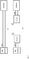
- a DALI interface allows a digital signal to be sent over two wires from a controller to a LED driver (see Fig. 1(a) ).
- the DALI control interface can be extended to include wireless devices as well.
- the two wires interface can be replaced by a wireless intermediate gateway, as shown in Fig. 1(b) .
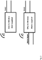
- Fig. 1(a) only the DALI wires are represented. However, most of the devices in the market are powered either via the DALI wires themselves or they possess their own power supply, for example from a mains converter (see Fig. 2 ).
- Devices with internal power supply may or may not have integrated DALI power supply.
- Devices with integrated DALI power supply provide energy to the DALI bus exclusively or in conjunction with another DALI power supply.
- the only restriction imposed by DALI in terms of paralleling DALI power supplies is that the total current circulating on the DALI bus cannot exceed the bus limit or 250 mA and the peak transient current of 450 mA. So, multiple power supplies can provide energy to the same bus.
- the invention relates to a communication gateway module having: a wireless interface, a wired bus interface comprising wired bus terminals, e.g. a DALI bus interface, a mains supply interface comprising mains voltage terminals; and a control circuit.
- the control circuit is configured to determine whether a mains voltage is supplied to the mains supply terminals and to power the gateway module in the positive case, and to determine whether a bus with non-zero quiescent state, such as e.g. a DALI bus, is connected to the wired bus terminals, and to power the gateway module off the wired bus terminals in case no mains voltage is supplied at mains voltage terminals.
- gateway module can be powered both by the mains supply or the wired bus interface, e.g. a DALI power supply.
- the communication gateway module further comprises a bus voltage supply unit for supplying the bus at the wired bus terminals with electrical power off the mains voltage terminals.
- the communication gateway module comprises a first current limiting circuit configured to limit any current drawn from the wired bus terminals.
- the communication gateway module comprises a second current limiting circuitry configured to limit any current supplied to the wired bus terminals.
- the communication gateway module comprises a circuitry for commutating the polarity of the voltage of the electrical power supplied to the bus at the wired bus terminals.
- the communication gateway module comprises an inverting stage configured to operate as a rectifier when supply is drawn from the bus terminals.
- the invention relates to an LED lighting system.
- the LED lighting system comprises a communication gateway module of the first aspect or any of its embodiments, and an LED driver.
- the invention relates to an LED luminaire.
- the luminaire comprises a communication gateway module of the first aspect or any of its embodiments; an LED driver; and a light source comprising one or more LEDs or OLEDs, the light source being operable by the LED driver.
- LED luminaire shall mean a luminaire with a light source comprising one or more LEDs or OLEDs. LEDs are well-known in the art, and therefore, will only briefly be discussed to provide a complete description of the invention.
- the aspect of the present invention might contain integrated circuits that are readily manufacturable using conventional semiconductor technologies, such as complementary metal-oxide semiconductor technology, short "CMOS".
- CMOS complementary metal-oxide semiconductor technology
- the aspects of the present invention may be implemented with other manufacturing processes for making optical as well as electrical devices.
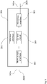
- a communication gateway module 300 is shown according to an embodiment.
- the communication gateway module 300 comprises a wireless interface 301 (antenna not shown), a wired bus interface 302 comprising wired bus terminals 302a, 302b, e.g. a DALI bus interface, a mains supply interface 303 comprising mains voltage terminals 303a, 303b; and a control circuit 304.
- the control circuit 304 controls the power supply of the communication gateway module 300 and the communication over the interfaces 301 and 302.
- the control circuit is connected to the interfaces 301, 302 and the mains supply interface 303.
- the communication gateway module 300 is configured to determine whether a mains voltage is supplied to the mains supply terminals 303a, 303b and to power the gateway module 300 in the positive case.
- the communication gateway module 300 is configured to determine whether a bus with non-zero quiescent state is connected to the wired bus terminals 302a, 302b, and to power the gateway module 300 off the wired bus terminals 302a, 302b in case no mains voltage is supplied at mains voltage terminals 303a, 303b.
- the communication gateway module 300 is configured to select its power source regardless of the sources available, DALI, internal power supply or both.
- the communication gateway module 300 can draw limited power from the DALI bus (limited meaning within the limitations of the DALI specification).
- the communication gateway module 300 is provided with mains supply terminals 303a and 303b.
- the control circuit 304 in the communication gateway module 300 can determine whether mains and/or DALI power supply is available at the respective terminals. In case mains power supply is available, the priority is on the mains power supply.
- the communication gateway module 300 is configured to select the supply source according to any one of the combinations shown in the table below and can possess an integrated DALI Power Supply (IDPS), see circuit 403 on Figure 4 , as well.
- IDPS integrated DALI Power Supply
- the communication gateway module 300 is provided with a circuitry to power the DALI bus, provided that it is itself provided with mains supply voltage.
- Fig. 4 shows a communication gateway module 300 according to an embodiment.
- an AC/DC converter 401 is arranged for being supplied with AC mains voltage from the terminals 303a and 303b and for outputting a DC voltage.
- the DV voltage is supplied e.g. to a low voltage power supply unit 402. Moreover, it provides energy to the control circuit 304 and its IDPS designated.
- the low voltage power supply (LVPS) 402 is configured to power the control circuit 304, off the DC voltage supplied by the AC/DC converter (401).
- the control circuit 304 may comprise a microcontroller and RF transceiver, both of which can be integrated as system-on-chip (SoC).
- a first current limiting circuit 403 is connected directly to the output of the AC/DC converter 401 and represents the IDPS according to this embodiment. It can be configured to limit the amount of current provided to the DALI bus according to the DALI specification.
- a second current limiting circuitry 404 limits the current in opposite direction to the first one, limiting the amount of current drawn from the DALI bus, when the DALI bus is used as main power source. Both circuits can be controllable by the control circuit 304 such that the control circuit can e.g. also disable them.
- Both current limiting circuitries can be bypassed by a semiconductor (e.g. diode) in anti-parallel position, to allow the current to flow in both directions.
- a semiconductor e.g. diode
- the control circuit 304 has a power supply and a RF control responsible for the DALI communications, RF communications and the control of the current limiting circuits 403, 404.
- a DALI TX and DALI RX interface 302 is is configured to receive and transmit according to DALI specifications. It is controlled by the control unit 304.
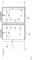
- Fig. 5 shows a flow chart 500 of an operation of the communication gateway module 300 according to an embodiment.
- step 504 it is checked if the mains voltage is present at the mains terminals. If yes, then in step 505 it is checked for an external power supply supplying the DALI bus with power. In particular, it is checked in step 508 if the DALI bus is high. If yes, then a configuration of the system or the communication gateway module 300 is checked in step 509. In particular, a user input can be used to determine whether the internal power supply IDPS of the communication gateway module 300 should or should not operate when the DALI bus is already powered. This ability provides flexibility to scale up the power of the communication gateway module 300 or to avoid exceeding the DALI system requirements. This input can be in many forms, such as configuration file, settings, button in interface, etc. Afterwards, it is checked if there is a multi-power supplied system in step 510. If yes, then the IDPS is enabled in step 507 and the DALI wireless gateway functions are resumed in step 506.
- step 504 If the mains is not present in step 504, then the communication gateway module 300 is powered by DALI supply in step 503 and the DALI wireless gateway functions are resumed in step 506.
- step 508 if the DALI bus is not high in step 508, then the IDPS is enabled in step 507 and, afterwards, the DALI wireless gateway functions are resumed in step 506.
- step510 the system or communication gateway module 300 is not a multi-power supplied system, then the DALI wireless gateway functions are resumed in step506.
- Fig. 6 shows the first current limiting circuit 403 and the second current limiting circuit 404 of a communication gateway module 300 according to an embodiment.
- the AC/DC converter 401 comprises a flyback converter for supplying a regulated DC voltage at a capacitor C1.
- the elements D7, R2, Q1, Q2, R1, D1, Q5 and VCTRL1 are part of DALI power supply and are used when the communication gateway module 300 is mains supplied and supplies DALI bus.
- the elements D6, R3, Q3, Q4, R5, D2, Q6, R4 and Q11 are part of the circuit used when the communication gateway module 300 is supplied by a DALI bus.
- the commands VCTRL1 and VCTRL2 are controller signals that are configured to enable and disable the current limiting circuits 403 and 404 depending on the mode of operation.
- the command VCTRL1 enables the DALI power supply when the communication gateway module 300 is mains supplied, while the command VCTRL2 disables the current limiting circuit 403 and 404 when the communication gateway module 300 is mains supplied.
- the command VCTRL1 disables the DALI power supply, while, when DALI bus power is supplied, the current limiting circuit 404 is automatically enabled via R4 and Q6 and can only be disabled via the command VCTRL2.
- Fig. 7 shows a first current limiting circuit 403, a second current limiting circuit 404 and an inverter/rectifying circuit 601 of a communication gateway module 300 according to an embodiment.
- the inverting stage 601 is added to the previous embodiment shown in Fig. 6 .
- the inverting/rectifying section 601 of the circuit allows any DALI polarity on the DALI bus by enabling Q7 and Q10 or Q8 and Q9 pairs.
- the DALI voltage polarity can be adjusted to match other power supplies on the bus, if existing.
- the diodes D4, D5, D8 and D9 rectify the DALI input voltage to allow any wire polarity connection.
- the inverter/rectifier circuitry 601 allows to switch the polarity of the voltage supplied to the DALI bus terminals 302a and 302b.
- LED lighting system and an LED luminaire according to an embodiments.
- the LED lighting system comprises a communication gateway module 300 according to an embodiment; and an LED driver.
- the LED luminaire comprises a communication gateway module 300 according to an embodiment; an LED driver; and a light source comprising one or more LEDs or OLEDs.
- the light source is operable by the LED driver.
Landscapes
- Engineering & Computer Science (AREA)
- Computer Networks & Wireless Communication (AREA)
- Small-Scale Networks (AREA)
- Remote Monitoring And Control Of Power-Distribution Networks (AREA)
Abstract
Description
- The invention relates, in general, to LED lighting wireless control modules. In particular, the invention relates to a communication gateway module for translating between a wired (e.g.) DALI bus communication and a (non-DALI) wireless communication.
- LED drivers, which comprise a control interface, allow their light output to be dynamically controlled. For example, the DALI control interface is one of the most common control interfaces used in LED lighting. In particular, a DALI interface allows a digital signal to be sent over two wires from a controller to a LED driver (see
Fig. 1(a) ). - The DALI control interface can be extended to include wireless devices as well. In this case, the two wires interface can be replaced by a wireless intermediate gateway, as shown in
Fig. 1(b) . - In
Fig. 1(a) , only the DALI wires are represented. However, most of the devices in the market are powered either via the DALI wires themselves or they possess their own power supply, for example from a mains converter (seeFig. 2 ). - Devices with internal power supply may or may not have integrated DALI power supply. Devices with integrated DALI power supply provide energy to the DALI bus exclusively or in conjunction with another DALI power supply. The only restriction imposed by DALI in terms of paralleling DALI power supplies is that the total current circulating on the DALI bus cannot exceed the bus limit or 250 mA and the peak transient current of 450 mA. So, multiple power supplies can provide energy to the same bus.
- However, inherently, these devices, in particular the communication gateway modules, when designed to be supplied via DALI or via an own power supply, are limited in their application.
- Thus, it is an objective to provide for an improved power supply for a wired bus/wireless communication gateway module.
- The object of the present invention is achieved by the solution provided in the enclosed independent claims. Advantageous implementations of the present invention are further defined in the dependent claims.
- According to a first aspect, the invention, relates to a communication gateway module having: a wireless interface, a wired bus interface comprising wired bus terminals, e.g. a DALI bus interface, a mains supply interface comprising mains voltage terminals; and a control circuit. The control circuit is configured to determine whether a mains voltage is supplied to the mains supply terminals and to power the gateway module in the positive case, and to determine whether a bus with non-zero quiescent state, such as e.g. a DALI bus, is connected to the wired bus terminals, and to power the gateway module off the wired bus terminals in case no mains voltage is supplied at mains voltage terminals.
- This provides the advantage that the gateway module can be powered both by the mains supply or the wired bus interface, e.g. a DALI power supply.
- In an embodiment, the communication gateway module further comprises a bus voltage supply unit for supplying the bus at the wired bus terminals with electrical power off the mains voltage terminals.
- This provides the advantage that power for supplying the bus can be taken from the mains voltage terminals if necessary.
- In an embodiment, the communication gateway module comprises a first current limiting circuit configured to limit any current drawn from the wired bus terminals.
- In an embodiment, the communication gateway module comprises a second current limiting circuitry configured to limit any current supplied to the wired bus terminals.
- In an embodiment, the communication gateway module comprises a circuitry for commutating the polarity of the voltage of the electrical power supplied to the bus at the wired bus terminals.
- In an embodiment, the communication gateway module comprises an inverting stage configured to operate as a rectifier when supply is drawn from the bus terminals.
- According to a second aspect, the invention relates to an LED lighting system. The LED lighting system comprises a communication gateway module of the first aspect or any of its embodiments, and an LED driver.
- According to a third aspect, the invention relates to an LED luminaire. The luminaire comprises a communication gateway module of the first aspect or any of its embodiments; an LED driver; and a light source comprising one or more LEDs or OLEDs, the light source being operable by the LED driver.
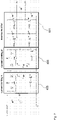
- The invention will be explained in the followings together with the figures.
- Fig. 1
- shows a DALI interface according to prior art;
- Fig. 2
- shows a DALI interface according to prior art;
- Fig. 3
- shows a communication gateway module according to an embodiment; and
- Fig. 4
- shows a communication gateway module according to an embodiment;
- Fig. 5
- shows a flow chart of a communication gateway module according to an embodiment;
- Fig. 6
- shows a first current limiting circuit and a second current limiting circuit of a communication gateway module according to an embodiment; and
- Fig. 7
- shows a first current limiting circuit, a second current limiting circuit and an inverter/rectifying circuit of a communication gateway module according to an embodiment.
- Aspects of the present invention are described herein in the context of a communication gateway module.
- The present invention is described more fully hereinafter with reference to the accompanying drawings, in which various aspects of the present invention are shown. This invention however may be embodied in many different forms and should not be construed as limited to the various aspects of the present invention presented through this disclosure. Rather, these aspects are provided so that this disclosure will be thorough and complete, and will fully convey the scope of the present invention to those skilled in the art. The various aspects of the present invention illustrated in the drawings may not be drawn to scale. Rather, the dimensions of the various features may be expanded or reduced for clarity. In addition, some of the drawings may be simplified for clarity. Thus, the drawings may not depict all of the components of a given apparatus.
- Various aspects of a communication gateway module will be presented. However, as those skilled in the art will readily appreciate, these aspects may be extended to aspects of communication gateway modules without departing from the invention.
- The term "LED luminaire" shall mean a luminaire with a light source comprising one or more LEDs or OLEDs. LEDs are well-known in the art, and therefore, will only briefly be discussed to provide a complete description of the invention.
- It is further understood that the aspect of the present invention might contain integrated circuits that are readily manufacturable using conventional semiconductor technologies, such as complementary metal-oxide semiconductor technology, short "CMOS". In addition, the aspects of the present invention may be implemented with other manufacturing processes for making optical as well as electrical devices. Reference will now be made in detail to implementations of the exemplary aspects as illustrated in the accompanying drawings. The same references signs will be used throughout the drawings and the following detailed descriptions to refer to the same or like parts.
- Now referring to
Fig. 3 , acommunication gateway module 300 is shown according to an embodiment. - The
communication gateway module 300 comprises a wireless interface 301 (antenna not shown), awired bus interface 302 comprising wiredbus terminals mains supply interface 303 comprisingmains voltage terminals control circuit 304. - The
control circuit 304 controls the power supply of thecommunication gateway module 300 and the communication over theinterfaces - The control circuit is connected to the
interfaces mains supply interface 303. - Further, the
communication gateway module 300 is configured to determine whether a mains voltage is supplied to themains supply terminals gateway module 300 in the positive case. - Sill further, the communication gateway module 300is configured to determine whether a bus with non-zero quiescent state is connected to the
wired bus terminals gateway module 300 off thewired bus terminals mains voltage terminals - This provides the advantage that the
communication gateway module 300 is configured to select its power source regardless of the sources available, DALI, internal power supply or both. - Moreover, if a DALI bus is connected, and the DALI bus has a bus supply by a dedicated bus supply unit or an integrated DALI power supply, for example in an operating device for lighting means, the
communication gateway module 300 can draw limited power from the DALI bus (limited meaning within the limitations of the DALI specification). - Further, the
communication gateway module 300 is provided withmains supply terminals control circuit 304 in thecommunication gateway module 300 can determine whether mains and/or DALI power supply is available at the respective terminals. In case mains power supply is available, the priority is on the mains power supply. - Moreover, the
communication gateway module 300 is configured to select the supply source according to any one of the combinations shown in the table below and can possess an integrated DALI Power Supply (IDPS), seecircuit 403 onFigure 4 , as well.AC Mains Powered DALI Bus Supply options IDPS Present Present Via mains Optional ON/OFF Present Absent Via mains ON Absent Present Via DALI OFF - In this manner, advantageously, all possible system scenarios are covered by a single configurable device or
communication gateway module 300. - Preferably, the
communication gateway module 300 is provided with a circuitry to power the DALI bus, provided that it is itself provided with mains supply voltage. -
Fig. 4 shows acommunication gateway module 300 according to an embodiment. - In
Fig. 4 , an AC/DC converter 401 is arranged for being supplied with AC mains voltage from theterminals power supply unit 402. Moreover, it provides energy to thecontrol circuit 304 and its IDPS designated. - The low voltage power supply (LVPS) 402 is configured to power the
control circuit 304, off the DC voltage supplied by the AC/DC converter (401). Thecontrol circuit 304 may comprise a microcontroller and RF transceiver, both of which can be integrated as system-on-chip (SoC). - A first current limiting
circuit 403 is connected directly to the output of the AC/DC converter 401 and represents the IDPS according to this embodiment. It can be configured to limit the amount of current provided to the DALI bus according to the DALI specification. - A second current limiting
circuitry 404 limits the current in opposite direction to the first one, limiting the amount of current drawn from the DALI bus, when the DALI bus is used as main power source. Both circuits can be controllable by thecontrol circuit 304 such that the control circuit can e.g. also disable them. - Both current limiting circuitries can be bypassed by a semiconductor (e.g. diode) in anti-parallel position, to allow the current to flow in both directions.
- The
control circuit 304 has a power supply and a RF control responsible for the DALI communications, RF communications and the control of the current limitingcircuits - A DALI TX and
DALI RX interface 302 is is configured to receive and transmit according to DALI specifications. It is controlled by thecontrol unit 304. -
Fig. 5 shows aflow chart 500 of an operation of thecommunication gateway module 300 according to an embodiment. - After the
start 501 the IDPS is disabled instep 502. Afterwards, instep 504 it is checked if the mains voltage is present at the mains terminals. If yes, then instep 505 it is checked for an external power supply supplying the DALI bus with power. In particular, it is checked instep 508 if the DALI bus is high. If yes, then a configuration of the system or thecommunication gateway module 300 is checked instep 509. In particular, a user input can be used to determine whether the internal power supply IDPS of thecommunication gateway module 300 should or should not operate when the DALI bus is already powered. This ability provides flexibility to scale up the power of thecommunication gateway module 300 or to avoid exceeding the DALI system requirements. This input can be in many forms, such as configuration file, settings, button in interface, etc. Afterwards, it is checked if there is a multi-power supplied system instep 510. If yes, then the IDPS is enabled instep 507 and the DALI wireless gateway functions are resumed instep 506. - If the mains is not present in
step 504, then thecommunication gateway module 300 is powered by DALI supply instep 503 and the DALI wireless gateway functions are resumed instep 506. - Moreover, if the DALI bus is not high in
step 508, then the IDPS is enabled instep 507 and, afterwards, the DALI wireless gateway functions are resumed instep 506. - Furthermore, if in step510 the system or
communication gateway module 300 is not a multi-power supplied system, then the DALI wireless gateway functions are resumed in step506. -
Fig. 6 shows the first current limitingcircuit 403 and the second current limitingcircuit 404 of acommunication gateway module 300 according to an embodiment. - In this embodiment, attention is payed to the current limiting
stages - In this embodiment, the AC/
DC converter 401 comprises a flyback converter for supplying a regulated DC voltage at a capacitor C1. The elements D7, R2, Q1, Q2, R1, D1, Q5 and VCTRL1 are part of DALI power supply and are used when thecommunication gateway module 300 is mains supplied and supplies DALI bus. - Moreover, the elements D6, R3, Q3, Q4, R5, D2, Q6, R4 and Q11 are part of the circuit used when the
communication gateway module 300 is supplied by a DALI bus. The commands VCTRL1 and VCTRL2 are controller signals that are configured to enable and disable the current limitingcircuits communication gateway module 300 is mains supplied, while the command VCTRL2 disables the current limitingcircuit communication gateway module 300 is mains supplied. - When DALI bus is already supplied from a source outside the
gateway module 300, the command VCTRL1 disables the DALI power supply, while, when DALI bus power is supplied, the current limitingcircuit 404 is automatically enabled via R4 and Q6 and can only be disabled via the command VCTRL2. -
Fig. 7 shows a first current limitingcircuit 403, a second current limitingcircuit 404 and an inverter/rectifying circuit 601 of acommunication gateway module 300 according to an embodiment. - In this embodiment, the inverting
stage 601 is added to the previous embodiment shown inFig. 6 . - In particular, the inverting/
rectifying section 601 of the circuit allows any DALI polarity on the DALI bus by enabling Q7 and Q10 or Q8 and Q9 pairs. The DALI voltage polarity can be adjusted to match other power supplies on the bus, if existing. When supplied from the DALI bus, the diodes D4, D5, D8 and D9 rectify the DALI input voltage to allow any wire polarity connection. - Moreover, especially in case a plurality of power supplies are active on the DALI bus, they all have to supply power with the same polarity to the DALI bus. The inverter/
rectifier circuitry 601 allows to switch the polarity of the voltage supplied to theDALI bus terminals - Not shown are an LED lighting system and an LED luminaire according to an embodiments.
- The LED lighting system comprises a
communication gateway module 300 according to an embodiment; and an LED driver. - The LED luminaire comprises a
communication gateway module 300 according to an embodiment; an LED driver; and a light source comprising one or more LEDs or OLEDs. The light source is operable by the LED driver. - All features of all embodiments described, shown and/or claimed herein can be combined with each other.
- While various embodiments of the present invention have been described above, it should be understood that they have been presented by way of example only and not limitation. Numerous changes to the disclosed embodiments can be made in accordance with the disclosure herein without departing from the spirit of scope of the invention. Thus, the breadth and scope of the present invention should not be limited by any of the above-described embodiments. Rather, the scope of the invention should be defined in accordance with the following claims and their equivalence.
- Although the invention has been illustrated and described with respect to one or more implementations, equivalent alternations and modifications will occur to those skilled in the art upon the reading of the understanding of the specification and the annexed drawings. In addition, while a particular feature of the invention may have been disclosed with respect to only of the several implementations, such features may be combined with one or more other features of the other implementations as may be desired and advantage for any given or particular application.
Claims (8)
- A communication gateway module (300) having:- a wireless interface (301),- a wired bus interface (302) comprising wired bus terminals (302a, 302b), e.g. a DALI bus interface,- a mains supply interface (303) comprising mains voltage terminals (303a, 303b); and- a control circuit (304) configured to:- determine whether a mains voltage is supplied to the mains supply terminals (303a, 303b) and to power the gateway module (300) in the positive case, and to- determine whether a bus with non-zero quiescent state is connected to the wired bus terminals (302a, 302b), and to power the gateway module (300) off the wired bus terminals (302a, 302b) in case no mains voltage is supplied at mains voltage terminals (303a, 303b).
- The communication gateway module (300) of claim 1, further comprising a bus voltage supply unit for supplying the bus at the wired bus terminals (302a, 302b), with electrical power off the mains voltage terminals (303a, 303b).
- The communication gateway module (300) of claim 1 or 2, comprising a first current limiting circuit (403) configured to limit any current drawn from the wired bus terminals (302a, 302b) .
- The communication gateway module (300) of claim 2, further comprising a second current limiting circuitry (404) configured to limit any current supplied to the wired bus terminals (302a, 302b).
- The communication gateway module (300) of any one of claims 2 or 4, further comprising an circuitry for commutating the polarity of the voltage of the electrical power supplied to the bus at the wired bus terminals (302a, 302b).
- The communication gateway module (300) of any one of the preceding claims, further comprising an inverting stage (601) configured to operate as a rectifier when supply is drawn from the bus terminals (302a, 302b).
- An LED lighting system, comprising
a communication gateway module (300) of any one of the claims 1 to 6; and
an LED driver. - An LED luminaire, comprising
a communication gateway module (300) of any one of the claims 1 to 6;
an LED driver; and
a light source comprising one or more LEDs or OLEDs, the light source being operable by the LED driver.
Priority Applications (2)
| Application Number | Priority Date | Filing Date | Title |
|---|---|---|---|
| EP21165124.5A EP4064797B1 (en) | 2021-03-26 | 2021-03-26 | Communication gateway module |
| PCT/EP2022/057511 WO2022200361A1 (en) | 2021-03-26 | 2022-03-22 | Communication gateway module |
Applications Claiming Priority (1)
| Application Number | Priority Date | Filing Date | Title |
|---|---|---|---|
| EP21165124.5A EP4064797B1 (en) | 2021-03-26 | 2021-03-26 | Communication gateway module |
Publications (2)
| Publication Number | Publication Date |
|---|---|
| EP4064797A1 true EP4064797A1 (en) | 2022-09-28 |
| EP4064797B1 EP4064797B1 (en) | 2023-12-27 |
Family
ID=75252356
Family Applications (1)
| Application Number | Title | Priority Date | Filing Date |
|---|---|---|---|
| EP21165124.5A Active EP4064797B1 (en) | 2021-03-26 | 2021-03-26 | Communication gateway module |
Country Status (2)
| Country | Link |
|---|---|
| EP (1) | EP4064797B1 (en) |
| WO (1) | WO2022200361A1 (en) |
Citations (3)
| Publication number | Priority date | Publication date | Assignee | Title |
|---|---|---|---|---|
| US20170231065A1 (en) * | 2014-10-30 | 2017-08-10 | Tridonic Gmbh & Co Kg | Method for Controlling an Operating Device for Lighting Means |
| GB2554987A (en) * | 2016-08-19 | 2018-04-18 | Leviton Manufacturing Co | Supplemental power system for power over ethernet lighting luminaries |
| WO2020194355A1 (en) * | 2019-03-26 | 2020-10-01 | Beghelli S.P.A. | Apparatus and method for a remote control of emergency lighting equipment |
-
2021
- 2021-03-26 EP EP21165124.5A patent/EP4064797B1/en active Active
-
2022
- 2022-03-22 WO PCT/EP2022/057511 patent/WO2022200361A1/en not_active Ceased
Patent Citations (3)
| Publication number | Priority date | Publication date | Assignee | Title |
|---|---|---|---|---|
| US20170231065A1 (en) * | 2014-10-30 | 2017-08-10 | Tridonic Gmbh & Co Kg | Method for Controlling an Operating Device for Lighting Means |
| GB2554987A (en) * | 2016-08-19 | 2018-04-18 | Leviton Manufacturing Co | Supplemental power system for power over ethernet lighting luminaries |
| WO2020194355A1 (en) * | 2019-03-26 | 2020-10-01 | Beghelli S.P.A. | Apparatus and method for a remote control of emergency lighting equipment |
Also Published As
| Publication number | Publication date |
|---|---|
| WO2022200361A1 (en) | 2022-09-29 |
| EP4064797B1 (en) | 2023-12-27 |
Similar Documents
| Publication | Publication Date | Title |
|---|---|---|
| CN111052864B (en) | Circuit for supplying power to components of lighting equipment and lighting equipment comprising the same | |
| US10548189B2 (en) | Control of isolated auxiliary power supply and DALI supply for sensor-ready LED drivers | |
| TWI578843B (en) | Driving circuit of light-emitting diodes | |
| KR101790046B1 (en) | Device and method for charging a master device using a detachable device | |
| EP2815492B1 (en) | Load driver and method for reducing the output ripple current of a load driver | |
| CN204707310U (en) | Multichannel light modulating device and apply its lighting device | |
| CN106549471A (en) | Management circuit | |
| EP4064797B1 (en) | Communication gateway module | |
| EP3057213A1 (en) | Apparatus for performing hybrid power control in an electronic device with aid of separated power output nodes for multi-purpose usage of boost | |
| US12526888B2 (en) | Control integrated circuit for controlling an operating device for lighting means; operating device; luminaire and method for operating a control integrated circuit | |
| CN216600133U (en) | LED power supply with constant luminous flux | |
| US9693404B1 (en) | Negative current sensing method for multi-channel LED driver | |
| CN209982778U (en) | Intelligent COB optical engine module | |
| EP3755123B1 (en) | Communication interface for lighting means | |
| US11317494B2 (en) | Linear luminance adjusting circuit | |
| US11765802B2 (en) | Isolated primary side switched converter for LED loads | |
| CN110071679B (en) | Motor control circuit | |
| KR102142638B1 (en) | Lighting apparatus operating based on current path switching | |
| US12062872B2 (en) | Adapter for electrically connecting a lighting device to an electrical track | |
| KR102620382B1 (en) | Electric vehicle charging module for producing high output from multiple low-output power modules and driving method thereof | |
| CN110771262B (en) | Apparatus and system for providing a power converter | |
| CN222283522U (en) | A driving circuit for LED lighting device | |
| CN214757024U (en) | Dimming circuit and dimming system | |
| KR101917593B1 (en) | A two-way SMPS(Switching Mode Power Supplier) powered by AC and DC | |
| CN212393020U (en) | Intelligent lighting device |
Legal Events
| Date | Code | Title | Description |
|---|---|---|---|
| PUAI | Public reference made under article 153(3) epc to a published international application that has entered the european phase |
Free format text: ORIGINAL CODE: 0009012 |
|
| STAA | Information on the status of an ep patent application or granted ep patent |
Free format text: STATUS: THE APPLICATION HAS BEEN PUBLISHED |
|
| AK | Designated contracting states |
Kind code of ref document: A1 Designated state(s): AL AT BE BG CH CY CZ DE DK EE ES FI FR GB GR HR HU IE IS IT LI LT LU LV MC MK MT NL NO PL PT RO RS SE SI SK SM TR |
|
| STAA | Information on the status of an ep patent application or granted ep patent |
Free format text: STATUS: REQUEST FOR EXAMINATION WAS MADE |
|
| 17P | Request for examination filed |
Effective date: 20230125 |
|
| RBV | Designated contracting states (corrected) |
Designated state(s): AL AT BE BG CH CY CZ DE DK EE ES FI FR GB GR HR HU IE IS IT LI LT LU LV MC MK MT NL NO PL PT RO RS SE SI SK SM TR |
|
| GRAP | Despatch of communication of intention to grant a patent |
Free format text: ORIGINAL CODE: EPIDOSNIGR1 |
|
| STAA | Information on the status of an ep patent application or granted ep patent |
Free format text: STATUS: GRANT OF PATENT IS INTENDED |
|
| INTG | Intention to grant announced |
Effective date: 20230831 |
|
| GRAS | Grant fee paid |
Free format text: ORIGINAL CODE: EPIDOSNIGR3 |
|
| GRAA | (expected) grant |
Free format text: ORIGINAL CODE: 0009210 |
|
| STAA | Information on the status of an ep patent application or granted ep patent |
Free format text: STATUS: THE PATENT HAS BEEN GRANTED |
|
| AK | Designated contracting states |
Kind code of ref document: B1 Designated state(s): AL AT BE BG CH CY CZ DE DK EE ES FI FR GB GR HR HU IE IS IT LI LT LU LV MC MK MT NL NO PL PT RO RS SE SI SK SM TR |
|
| REG | Reference to a national code |
Ref country code: GB Ref legal event code: FG4D |
|
| REG | Reference to a national code |
Ref country code: DE Ref legal event code: R084 Ref document number: 602021007990 Country of ref document: DE Ref country code: CH Ref legal event code: EP |
|
| P01 | Opt-out of the competence of the unified patent court (upc) registered |
Effective date: 20231130 |
|
| REG | Reference to a national code |
Ref country code: DE Ref legal event code: R096 Ref document number: 602021007990 Country of ref document: DE |
|
| REG | Reference to a national code |
Ref country code: IE Ref legal event code: FG4D |
|
| PG25 | Lapsed in a contracting state [announced via postgrant information from national office to epo] |
Ref country code: GR Free format text: LAPSE BECAUSE OF FAILURE TO SUBMIT A TRANSLATION OF THE DESCRIPTION OR TO PAY THE FEE WITHIN THE PRESCRIBED TIME-LIMIT Effective date: 20240328 |
|
| REG | Reference to a national code |
Ref country code: LT Ref legal event code: MG9D |
|
| PG25 | Lapsed in a contracting state [announced via postgrant information from national office to epo] |
Ref country code: LT Free format text: LAPSE BECAUSE OF FAILURE TO SUBMIT A TRANSLATION OF THE DESCRIPTION OR TO PAY THE FEE WITHIN THE PRESCRIBED TIME-LIMIT Effective date: 20231227 |
|
| PG25 | Lapsed in a contracting state [announced via postgrant information from national office to epo] |
Ref country code: ES Free format text: LAPSE BECAUSE OF FAILURE TO SUBMIT A TRANSLATION OF THE DESCRIPTION OR TO PAY THE FEE WITHIN THE PRESCRIBED TIME-LIMIT Effective date: 20231227 |
|
| PG25 | Lapsed in a contracting state [announced via postgrant information from national office to epo] |
Ref country code: LT Free format text: LAPSE BECAUSE OF FAILURE TO SUBMIT A TRANSLATION OF THE DESCRIPTION OR TO PAY THE FEE WITHIN THE PRESCRIBED TIME-LIMIT Effective date: 20231227 Ref country code: GR Free format text: LAPSE BECAUSE OF FAILURE TO SUBMIT A TRANSLATION OF THE DESCRIPTION OR TO PAY THE FEE WITHIN THE PRESCRIBED TIME-LIMIT Effective date: 20240328 Ref country code: FI Free format text: LAPSE BECAUSE OF FAILURE TO SUBMIT A TRANSLATION OF THE DESCRIPTION OR TO PAY THE FEE WITHIN THE PRESCRIBED TIME-LIMIT Effective date: 20231227 Ref country code: ES Free format text: LAPSE BECAUSE OF FAILURE TO SUBMIT A TRANSLATION OF THE DESCRIPTION OR TO PAY THE FEE WITHIN THE PRESCRIBED TIME-LIMIT Effective date: 20231227 Ref country code: BG Free format text: LAPSE BECAUSE OF FAILURE TO SUBMIT A TRANSLATION OF THE DESCRIPTION OR TO PAY THE FEE WITHIN THE PRESCRIBED TIME-LIMIT Effective date: 20240327 |
|
| REG | Reference to a national code |
Ref country code: NL Ref legal event code: MP Effective date: 20231227 |
|
| REG | Reference to a national code |
Ref country code: AT Ref legal event code: MK05 Ref document number: 1645767 Country of ref document: AT Kind code of ref document: T Effective date: 20231227 |
|
| PG25 | Lapsed in a contracting state [announced via postgrant information from national office to epo] |
Ref country code: NL Free format text: LAPSE BECAUSE OF FAILURE TO SUBMIT A TRANSLATION OF THE DESCRIPTION OR TO PAY THE FEE WITHIN THE PRESCRIBED TIME-LIMIT Effective date: 20231227 |
|
| PG25 | Lapsed in a contracting state [announced via postgrant information from national office to epo] |
Ref country code: SE Free format text: LAPSE BECAUSE OF FAILURE TO SUBMIT A TRANSLATION OF THE DESCRIPTION OR TO PAY THE FEE WITHIN THE PRESCRIBED TIME-LIMIT Effective date: 20231227 Ref country code: RS Free format text: LAPSE BECAUSE OF FAILURE TO SUBMIT A TRANSLATION OF THE DESCRIPTION OR TO PAY THE FEE WITHIN THE PRESCRIBED TIME-LIMIT Effective date: 20231227 Ref country code: NO Free format text: LAPSE BECAUSE OF FAILURE TO SUBMIT A TRANSLATION OF THE DESCRIPTION OR TO PAY THE FEE WITHIN THE PRESCRIBED TIME-LIMIT Effective date: 20240327 Ref country code: NL Free format text: LAPSE BECAUSE OF FAILURE TO SUBMIT A TRANSLATION OF THE DESCRIPTION OR TO PAY THE FEE WITHIN THE PRESCRIBED TIME-LIMIT Effective date: 20231227 Ref country code: LV Free format text: LAPSE BECAUSE OF FAILURE TO SUBMIT A TRANSLATION OF THE DESCRIPTION OR TO PAY THE FEE WITHIN THE PRESCRIBED TIME-LIMIT Effective date: 20231227 Ref country code: HR Free format text: LAPSE BECAUSE OF FAILURE TO SUBMIT A TRANSLATION OF THE DESCRIPTION OR TO PAY THE FEE WITHIN THE PRESCRIBED TIME-LIMIT Effective date: 20231227 |
|
| PG25 | Lapsed in a contracting state [announced via postgrant information from national office to epo] |
Ref country code: IS Free format text: LAPSE BECAUSE OF FAILURE TO SUBMIT A TRANSLATION OF THE DESCRIPTION OR TO PAY THE FEE WITHIN THE PRESCRIBED TIME-LIMIT Effective date: 20240427 |
|
| PG25 | Lapsed in a contracting state [announced via postgrant information from national office to epo] |
Ref country code: CZ Free format text: LAPSE BECAUSE OF FAILURE TO SUBMIT A TRANSLATION OF THE DESCRIPTION OR TO PAY THE FEE WITHIN THE PRESCRIBED TIME-LIMIT Effective date: 20231227 Ref country code: AT Free format text: LAPSE BECAUSE OF FAILURE TO SUBMIT A TRANSLATION OF THE DESCRIPTION OR TO PAY THE FEE WITHIN THE PRESCRIBED TIME-LIMIT Effective date: 20231227 |
|
| PG25 | Lapsed in a contracting state [announced via postgrant information from national office to epo] |
Ref country code: SK Free format text: LAPSE BECAUSE OF FAILURE TO SUBMIT A TRANSLATION OF THE DESCRIPTION OR TO PAY THE FEE WITHIN THE PRESCRIBED TIME-LIMIT Effective date: 20231227 |
|
| PG25 | Lapsed in a contracting state [announced via postgrant information from national office to epo] |
Ref country code: SM Free format text: LAPSE BECAUSE OF FAILURE TO SUBMIT A TRANSLATION OF THE DESCRIPTION OR TO PAY THE FEE WITHIN THE PRESCRIBED TIME-LIMIT Effective date: 20231227 Ref country code: SK Free format text: LAPSE BECAUSE OF FAILURE TO SUBMIT A TRANSLATION OF THE DESCRIPTION OR TO PAY THE FEE WITHIN THE PRESCRIBED TIME-LIMIT Effective date: 20231227 Ref country code: RO Free format text: LAPSE BECAUSE OF FAILURE TO SUBMIT A TRANSLATION OF THE DESCRIPTION OR TO PAY THE FEE WITHIN THE PRESCRIBED TIME-LIMIT Effective date: 20231227 Ref country code: IT Free format text: LAPSE BECAUSE OF FAILURE TO SUBMIT A TRANSLATION OF THE DESCRIPTION OR TO PAY THE FEE WITHIN THE PRESCRIBED TIME-LIMIT Effective date: 20231227 Ref country code: IS Free format text: LAPSE BECAUSE OF FAILURE TO SUBMIT A TRANSLATION OF THE DESCRIPTION OR TO PAY THE FEE WITHIN THE PRESCRIBED TIME-LIMIT Effective date: 20240427 Ref country code: EE Free format text: LAPSE BECAUSE OF FAILURE TO SUBMIT A TRANSLATION OF THE DESCRIPTION OR TO PAY THE FEE WITHIN THE PRESCRIBED TIME-LIMIT Effective date: 20231227 Ref country code: CZ Free format text: LAPSE BECAUSE OF FAILURE TO SUBMIT A TRANSLATION OF THE DESCRIPTION OR TO PAY THE FEE WITHIN THE PRESCRIBED TIME-LIMIT Effective date: 20231227 Ref country code: AT Free format text: LAPSE BECAUSE OF FAILURE TO SUBMIT A TRANSLATION OF THE DESCRIPTION OR TO PAY THE FEE WITHIN THE PRESCRIBED TIME-LIMIT Effective date: 20231227 |
|
| PG25 | Lapsed in a contracting state [announced via postgrant information from national office to epo] |
Ref country code: PL Free format text: LAPSE BECAUSE OF FAILURE TO SUBMIT A TRANSLATION OF THE DESCRIPTION OR TO PAY THE FEE WITHIN THE PRESCRIBED TIME-LIMIT Effective date: 20231227 Ref country code: PT Free format text: LAPSE BECAUSE OF FAILURE TO SUBMIT A TRANSLATION OF THE DESCRIPTION OR TO PAY THE FEE WITHIN THE PRESCRIBED TIME-LIMIT Effective date: 20240429 |
|
| PG25 | Lapsed in a contracting state [announced via postgrant information from national office to epo] |
Ref country code: PT Free format text: LAPSE BECAUSE OF FAILURE TO SUBMIT A TRANSLATION OF THE DESCRIPTION OR TO PAY THE FEE WITHIN THE PRESCRIBED TIME-LIMIT Effective date: 20240429 Ref country code: PL Free format text: LAPSE BECAUSE OF FAILURE TO SUBMIT A TRANSLATION OF THE DESCRIPTION OR TO PAY THE FEE WITHIN THE PRESCRIBED TIME-LIMIT Effective date: 20231227 |
|
| REG | Reference to a national code |
Ref country code: DE Ref legal event code: R097 Ref document number: 602021007990 Country of ref document: DE |
|
| PG25 | Lapsed in a contracting state [announced via postgrant information from national office to epo] |
Ref country code: DK Free format text: LAPSE BECAUSE OF FAILURE TO SUBMIT A TRANSLATION OF THE DESCRIPTION OR TO PAY THE FEE WITHIN THE PRESCRIBED TIME-LIMIT Effective date: 20231227 |
|
| PG25 | Lapsed in a contracting state [announced via postgrant information from national office to epo] |
Ref country code: DK Free format text: LAPSE BECAUSE OF FAILURE TO SUBMIT A TRANSLATION OF THE DESCRIPTION OR TO PAY THE FEE WITHIN THE PRESCRIBED TIME-LIMIT Effective date: 20231227 |
|
| REG | Reference to a national code |
Ref country code: CH Ref legal event code: PL |
|
| PLBE | No opposition filed within time limit |
Free format text: ORIGINAL CODE: 0009261 |
|
| STAA | Information on the status of an ep patent application or granted ep patent |
Free format text: STATUS: NO OPPOSITION FILED WITHIN TIME LIMIT |
|
| PG25 | Lapsed in a contracting state [announced via postgrant information from national office to epo] |
Ref country code: LU Free format text: LAPSE BECAUSE OF NON-PAYMENT OF DUE FEES Effective date: 20240326 |
|
| PG25 | Lapsed in a contracting state [announced via postgrant information from national office to epo] |
Ref country code: MC Free format text: LAPSE BECAUSE OF FAILURE TO SUBMIT A TRANSLATION OF THE DESCRIPTION OR TO PAY THE FEE WITHIN THE PRESCRIBED TIME-LIMIT Effective date: 20231227 |
|
| PG25 | Lapsed in a contracting state [announced via postgrant information from national office to epo] |
Ref country code: MC Free format text: LAPSE BECAUSE OF FAILURE TO SUBMIT A TRANSLATION OF THE DESCRIPTION OR TO PAY THE FEE WITHIN THE PRESCRIBED TIME-LIMIT Effective date: 20231227 Ref country code: LU Free format text: LAPSE BECAUSE OF NON-PAYMENT OF DUE FEES Effective date: 20240326 |
|
| 26N | No opposition filed |
Effective date: 20240930 |
|
| REG | Reference to a national code |
Ref country code: BE Ref legal event code: MM Effective date: 20240331 |
|
| PG25 | Lapsed in a contracting state [announced via postgrant information from national office to epo] |
Ref country code: BE Free format text: LAPSE BECAUSE OF NON-PAYMENT OF DUE FEES Effective date: 20240331 |
|
| PG25 | Lapsed in a contracting state [announced via postgrant information from national office to epo] |
Ref country code: IE Free format text: LAPSE BECAUSE OF NON-PAYMENT OF DUE FEES Effective date: 20240326 |
|
| PG25 | Lapsed in a contracting state [announced via postgrant information from national office to epo] |
Ref country code: IE Free format text: LAPSE BECAUSE OF NON-PAYMENT OF DUE FEES Effective date: 20240326 Ref country code: BE Free format text: LAPSE BECAUSE OF NON-PAYMENT OF DUE FEES Effective date: 20240331 Ref country code: CH Free format text: LAPSE BECAUSE OF NON-PAYMENT OF DUE FEES Effective date: 20240331 |
|
| PG25 | Lapsed in a contracting state [announced via postgrant information from national office to epo] |
Ref country code: SI Free format text: LAPSE BECAUSE OF FAILURE TO SUBMIT A TRANSLATION OF THE DESCRIPTION OR TO PAY THE FEE WITHIN THE PRESCRIBED TIME-LIMIT Effective date: 20231227 |
|
| PG25 | Lapsed in a contracting state [announced via postgrant information from national office to epo] |
Ref country code: CY Free format text: LAPSE BECAUSE OF FAILURE TO SUBMIT A TRANSLATION OF THE DESCRIPTION OR TO PAY THE FEE WITHIN THE PRESCRIBED TIME-LIMIT; INVALID AB INITIO Effective date: 20210326 |
|
| PG25 | Lapsed in a contracting state [announced via postgrant information from national office to epo] |
Ref country code: HU Free format text: LAPSE BECAUSE OF FAILURE TO SUBMIT A TRANSLATION OF THE DESCRIPTION OR TO PAY THE FEE WITHIN THE PRESCRIBED TIME-LIMIT; INVALID AB INITIO Effective date: 20210326 |
|
| PG25 | Lapsed in a contracting state [announced via postgrant information from national office to epo] |
Ref country code: TR Free format text: LAPSE BECAUSE OF FAILURE TO SUBMIT A TRANSLATION OF THE DESCRIPTION OR TO PAY THE FEE WITHIN THE PRESCRIBED TIME-LIMIT Effective date: 20231227 |
|
| PGFP | Annual fee paid to national office [announced via postgrant information from national office to epo] |
Ref country code: GB Payment date: 20260323 Year of fee payment: 6 |
|
| PGFP | Annual fee paid to national office [announced via postgrant information from national office to epo] |
Ref country code: DE Payment date: 20260320 Year of fee payment: 6 |
|
| PGFP | Annual fee paid to national office [announced via postgrant information from national office to epo] |
Ref country code: FR Payment date: 20260323 Year of fee payment: 6 |