EP4064457A1 - Single-layer air waveguide antenna integrated on circuit board - Google Patents
Single-layer air waveguide antenna integrated on circuit board Download PDFInfo
- Publication number
- EP4064457A1 EP4064457A1 EP22159217.3A EP22159217A EP4064457A1 EP 4064457 A1 EP4064457 A1 EP 4064457A1 EP 22159217 A EP22159217 A EP 22159217A EP 4064457 A1 EP4064457 A1 EP 4064457A1
- Authority
- EP
- European Patent Office
- Prior art keywords
- circuit board
- air
- single layer
- channels filled
- channels
- Prior art date
- Legal status (The legal status is an assumption and is not a legal conclusion. Google has not performed a legal analysis and makes no representation as to the accuracy of the status listed.)
- Pending
Links
Images






Classifications
-
- H—ELECTRICITY
- H01—ELECTRIC ELEMENTS
- H01Q—ANTENNAS, i.e. RADIO AERIALS
- H01Q1/00—Details of, or arrangements associated with, antennas
- H01Q1/27—Adaptation for use in or on movable bodies
- H01Q1/32—Adaptation for use in or on road or rail vehicles
- H01Q1/3208—Adaptation for use in or on road or rail vehicles characterised by the application wherein the antenna is used
- H01Q1/3233—Adaptation for use in or on road or rail vehicles characterised by the application wherein the antenna is used particular used as part of a sensor or in a security system, e.g. for automotive radar, navigation systems
-
- H—ELECTRICITY
- H01—ELECTRIC ELEMENTS
- H01Q—ANTENNAS, i.e. RADIO AERIALS
- H01Q1/00—Details of, or arrangements associated with, antennas
- H01Q1/36—Structural form of radiating elements, e.g. cone, spiral, umbrella; Particular materials used therewith
- H01Q1/38—Structural form of radiating elements, e.g. cone, spiral, umbrella; Particular materials used therewith formed by a conductive layer on an insulating support
-
- H—ELECTRICITY
- H01—ELECTRIC ELEMENTS
- H01P—WAVEGUIDES; RESONATORS, LINES, OR OTHER DEVICES OF THE WAVEGUIDE TYPE
- H01P11/00—Apparatus or processes specially adapted for manufacturing waveguides or resonators, lines, or other devices of the waveguide type
- H01P11/001—Manufacturing waveguides or transmission lines of the waveguide type
- H01P11/002—Manufacturing hollow waveguides
-
- H—ELECTRICITY
- H01—ELECTRIC ELEMENTS
- H01P—WAVEGUIDES; RESONATORS, LINES, OR OTHER DEVICES OF THE WAVEGUIDE TYPE
- H01P3/00—Waveguides; Transmission lines of the waveguide type
- H01P3/12—Hollow waveguides
- H01P3/121—Hollow waveguides integrated in a substrate
-
- H—ELECTRICITY
- H01—ELECTRIC ELEMENTS
- H01P—WAVEGUIDES; RESONATORS, LINES, OR OTHER DEVICES OF THE WAVEGUIDE TYPE
- H01P5/00—Coupling devices of the waveguide type
- H01P5/08—Coupling devices of the waveguide type for linking dissimilar lines or devices
- H01P5/10—Coupling devices of the waveguide type for linking dissimilar lines or devices for coupling balanced lines or devices with unbalanced lines or devices
- H01P5/107—Hollow-waveguide/strip-line transitions
-
- H—ELECTRICITY
- H01—ELECTRIC ELEMENTS
- H01Q—ANTENNAS, i.e. RADIO AERIALS
- H01Q13/00—Waveguide horns or mouths; Slot antennas; Leaky-waveguide antennas; Equivalent structures causing radiation along the transmission path of a guided wave
- H01Q13/20—Non-resonant leaky-waveguide or transmission-line antennas; Equivalent structures causing radiation along the transmission path of a guided wave
- H01Q13/22—Longitudinal slot in boundary wall of waveguide or transmission line
-
- H—ELECTRICITY
- H01—ELECTRIC ELEMENTS
- H01Q—ANTENNAS, i.e. RADIO AERIALS
- H01Q21/00—Antenna arrays or systems
- H01Q21/0006—Particular feeding systems
- H01Q21/0037—Particular feeding systems linear waveguide fed arrays
- H01Q21/0043—Slotted waveguides
-
- H—ELECTRICITY
- H05—ELECTRIC TECHNIQUES NOT OTHERWISE PROVIDED FOR
- H05K—PRINTED CIRCUITS; CASINGS OR CONSTRUCTIONAL DETAILS OF ELECTRIC APPARATUS; MANUFACTURE OF ASSEMBLAGES OF ELECTRICAL COMPONENTS
- H05K1/00—Printed circuits
- H05K1/18—Printed circuits structurally associated with non-printed electric components
-
- G—PHYSICS
- G01—MEASURING; TESTING
- G01S—RADIO DIRECTION-FINDING; RADIO NAVIGATION; DETERMINING DISTANCE OR VELOCITY BY USE OF RADIO WAVES; LOCATING OR PRESENCE-DETECTING BY USE OF THE REFLECTION OR RERADIATION OF RADIO WAVES; ANALOGOUS ARRANGEMENTS USING OTHER WAVES
- G01S7/00—Details of systems according to groups G01S13/00, G01S15/00, G01S17/00
- G01S7/02—Details of systems according to groups G01S13/00, G01S15/00, G01S17/00 of systems according to group G01S13/00
- G01S7/03—Details of HF subsystems specially adapted therefor, e.g. common to transmitter and receiver
- G01S7/032—Constructional details for solid-state radar subsystems
Definitions
- Air waveguides are used in many applications, for example, as antennas to shape or filter, based on frequency, an electromagnetic energy beam.
- Channels filled with air are some of the internal features of an air waveguide. These channels may include openings, referred to as radiators or slots, that allow electromagnetic energy to be filtered in or filtered out.
- Some waveguide channels may be formed from multiple layers of substrate material, stacked, and soldered together to form walls of a channel.
- Other air waveguides have been formed using Teflon and FR4 Printed Circuit Board (PCB) materials.
- Still some other air waveguides are manufactured using injection molded plastics (e.g., filled Polyetherimide (PEI)) that are given a metal coating (e.g., silver). Forming air waveguides using existing manufacturing techniques can be too expensive for some applications, including an automotive context where eventual mass-production is desired.
- PEI Polyetherimide
- an apparatus in one example, includes an air waveguide antenna configured to guide electromagnetic energy through channels filled with air.
- the air waveguide includes an electrical interface to a circuit board and a single layer of material having conductive surfaces positioned atop the electrical interface.
- the electrical interface configures a portion of a surface of the circuit board to act as a floor of the channels filled with air.
- the single layer of material defines walls and a ceiling of the channels filled with air.
- a method in another example, includes identifying a portion of a surface of a circuit board to act as an electrical interface to waveguide channels filled with air. The method further includes obtaining a single layer of material with conductive surfaces that define walls and a ceiling of the waveguide channels filled with air, and positioning the single layer of material atop the portion of the surface of the circuit board. The method further includes attaching the single layer of material to the portion of the surface of the circuit board to form an air waveguide antenna that is configured to guide electromagnetic energy through the waveguide channels filled with air.
- Radar systems are a sensing technology that some automotive systems rely on to acquire information about the surrounding environment. Radar systems generally use an antenna or a waveguide to direct electromagnetic energy or signals being transmitted or received. Such radar systems may use any combination of antennas and waveguides to provide increased gain and directivity. As the automotive industry increasingly utilizes radar systems in more vehicles, the challenge to reduce costs associated with waveguides for these radar systems becomes a higher priority for manufacturers.
- Air waveguides are used in many applications, for example, as antennas to shape or filter, based on frequency, an electromagnetic energy beam.
- Channels filled with air are some of the internal features of an air waveguide. These channels may include openings, referred to as radiators or slots, that allow electromagnetic energy to be filtered in or filtered out.
- Some waveguide channels may be formed from multiple layers of substrate material, stacked, and soldered together to form walls of the channels.
- Other air waveguides have been formed using Teflon and FR4 Printed Circuit Board (PCB) materials.
- Still some other air waveguides are manufactured using injection molded plastics (e.g., filled Polyetherimide (PEI)) that are given a metal coating (e.g., silver) under precisely controlled conditions so as to avoid thermal wear.
- PEI Polyetherimide
- Forming air waveguides using existing manufacturing techniques can be too expensive for some applications, including an automotive context where eventual mass-production is desired. Lower cost, but still high performance, air waveguide antenna technologies that make radar
- the waveguide guides electromagnetic energy through channels filled with air. It is formed from a single layer of material, such as a sheet of metal, metal-coated plastic, or other material with conductive surfaces that is attached to a circuit board. A portion of a surface of the circuit board is configured as a floor of the channels filled with air. This floor forms an electrical interface between the circuit board and the channels filled with air. The single layer of material is positioned atop this electrical interface to define walls and a ceiling of the channels filled with air. The single layer of material can be secured to the circuit board in various ways. The cost of integrating an air waveguide antenna onto a circuit board this way may be less expensive than other waveguide-manufacturing techniques.
- the example air waveguide antenna can be manufactured by stacking the single-layer material atop the circuit board, the two materials may be held together by a mechanical interface arranged between two adjacent surfaces.
- the mechanical interface may further include an electrical interface between the upper portion of the air waveguide antenna that is formed from the single layer of material, and the lower portion of the air waveguide antenna that is formed from the circuit board.
- the circuit board may include one or more electrical contacts that align with the channels of the air waveguide antenna so that the mechanical interface also electrically couples the two layers. This interface may eliminate a need for solder between connections that can be made directly through the interface formed between the two materials.
- the air waveguide antenna may, therefore, be far easier and less expensive to manufacture than existing waveguide technology.
- FIG. 1 illustrates an example environment 100 in which a radar system 102 with a single layer 104 air waveguide antenna 106 is integrated on a circuit board 108 and configured for use on a vehicle 110.
- the vehicle 110 may use one or more air waveguide antennas 106 to enable operations of the radar system 102.
- the vehicle 110 responsive to receiving, from the radar system 102, radar data indicative of a position of an object 112 relative a position of the vehicle 110, the vehicle 110 performs a driving-maneuver to avoid a collision with the object 112.
- the vehicle 110 can represent other types of motorized vehicles (e.g., a motorcycle, a bus, a tractor, a semi-trailer truck, or construction equipment), non-motorized vehicles (e.g., a bicycle), railed vehicles (e.g., a train or a trolley car), watercraft (e.g., a boat or a ship), aircraft (e.g., an airplane or a helicopter), or spacecraft (e.g., satellite).
- manufacturers can mount the radar system 102 to any moving platform, including moving machinery or robotic equipment.
- other devices e.g., desktop computers, tablets, laptops, televisions, computing watches, smartphones, gaming systems, and so forth
- the radar system 102 can be part of the vehicle 110.
- the radar system 102 is mounted near, or integrated within, a front portion of the vehicle 110 to detect the object 112 and avoid collisions.
- the radar system 102 provides a field-of-view 118 towards the object 112.
- the radar system 102 can project the field-of-view 118 from any exterior surface of the vehicle 110.
- vehicle manufacturers can integrate the radar system 102 into a bumper, side mirror, headlights, rear lights, or any other interior or exterior location where the object 112 requires detection.
- the vehicle 110 includes multiple radar systems 102, such as a first radar system 102 and a second radar system 102 that provide a larger field-of-view 118.
- vehicle manufacturers can design the locations of the one or more radar systems 102 to provide a particular field-of-view 118 that encompasses a region of interest, including, for instance, in or around a travel lane aligned with a vehicle path.
- the vehicle 110 can also include at least one automotive system that relies on data from the radar system 102, including a driver-assistance system, an autonomous-driving system, or a semi-autonomous-driving system.
- the radar system 102 can include an interface to such automotive systems.
- a signal can be output, via the interface, based on electromagnetic energy received by the radar system 102.
- the automotive systems use radar data provided by the radar system 102 to perform a function.
- the driver-assistance system can provide blind-spot monitoring and generate an alert indicating a potential collision with the object 112 detected by the radar system 102.
- the radar data from the radar system 102 indicate when it is safe or unsafe to change lanes.
- the autonomous-driving system may move the vehicle 110 to a particular location on the road while avoiding collisions with the object 112 detected by the radar system 102.
- the radar data provided by the radar system 102 can provide information about a distance to and the location of the object 112 to enable the autonomous-driving system to perform emergency braking, perform a lane change, or adjust the speed of the vehicle 110.
- the radar system 102 generally includes a transmitter (not illustrated) and at least one antenna, including the air waveguide antenna 106, to transmit electromagnetic signals.
- the radar system 102 generally includes a receiver (not illustrated) and at least one antenna, including the air waveguide antenna 106, to receive reflected versions of these electromagnetic signals.
- the transmitter includes components for emitting electromagnetic signals.
- the receiver includes components to detect the reflected electromagnetic signals.
- the transmitter and the receiver can be incorporated together on the same integrated circuit (e.g., a transceiver integrated circuit) or separately on different integrated circuits.
- the radar system 102 also includes one or more processors (not illustrated) and computer-readable storage media (CRM) (not illustrated).
- the processor can be a microprocessor or a system-on-chip. The processor executes instructions stored within the CRM.
- the processor can control the operation of the transmitter.
- the processor can also process electromagnetic energy received by the air waveguide antenna 106 and determine the location of the object 112 relative to the radar system 102.
- the processor can also generate radar data for the automotive systems.
- the processor can control, based on processed electromagnetic energy from the air waveguide antenna 106, an autonomous or semi-autonomous driving system of the vehicle 110.
- the air waveguide antenna 106 consists of just two main parts.
- a first main part consists of a metal or metalized-plastic layer 104 defining openings 116 (e.g., ports and radiators) into channels 114 that are filled with a dielectric, which in this example is air.
- the channels 114 are partially surrounded by vertical walls 120 and a ceiling 122.
- the purpose of the channels 114 is to guide desirable electromagnetic energy that is captured by the air waveguide antenna 106 to or from other components of the radar system 102 (e.g., a transceiver).
- a second main part of the air waveguide antenna 106 consists of a portion of the circuit board 108 (e.g., a substrate or other circuit board).
- the single layer 104 is integrated on and attached to the circuit board 108 so as to define the channels 114 that contain the dielectric (e.g., air).
- the vertical walls 120 that form the channels 114 within the first main part of the air waveguide antenna 106 are mated to a surface of the circuit board 108 that is configured to define a floor 124 of the channels 114.
- the floor 124 is arranged opposite (e.g., substantially parallel to) the ceiling 12.
- the single layer 104 can be formed of a single sheet of metal that is stamped or bent to take on a particular shape.
- the single layer 104 may consist of a metalized plastic; a surface coating of metal material may be applied to an injection-molded or printed plastic part that is at the desired shape.
- the single layer 104 of material may include a non-conductive core and an outer conductive surface.
- the non-conductive core of the single layer 104 of material may include plastic and the outer conductive surface may include metal.
- the air waveguide antenna 106 includes two channels 114.
- the channels 114 define a rectangular cavity surrounded by three vertical walls 120 with an opening at one end.
- the channels 114 and the openings 116 manipulate the electromagnetic energy in a manner that is advantageous for a particular application of the air waveguide antenna 106.
- the vertical walls 120 of the channels 114 e.g., surfaces of the channels 114 that are perpendicular relative to the flow of electromagnetic energy that passes through the channels 114) guide the electromagnetic energy in a lateral direction across a surface of the circuit board 108.
- the ceiling 122 and the floor 124 of the channels 114 regulate, in a perpendicular direction, in-flow and out-flow of the electromagnetic energy through the openings 116.
- the single layer 104 includes the openings 116 through the ceiling 122 and into the channels 114, which permit undesirable electromagnetic energy (e.g., energy that is outside an operating frequency) to escape the air waveguide 106, and which allow desirable electromagnetic energy (e.g., energy that is inside the operating frequency) to flow within the air waveguide 106.
- the openings 116 allow electromagnetic energy to enter the channels 114 (e.g., acting as ports) and exit the channels 114 (e.g., acting as radiators or slots).
- the floor 124 of the channels 114 which is provided by the circuit board 108, prevents electromagnetic energy that passes through the channels 114 from escaping the air waveguide 106 through the circuit board 108.
- the floor 124 of the channels 114 is formed by an exterior surface of the circuit board 108 that is in contact with the vertical walls 120 of the single layer 104.
- the floor 124 of the channels 114 may include a connection to a wire, a pad, or a trace that electrically couples the air waveguide antenna 106 to other components of the radar system 102, for instance, other components (not shown) that are integrated on or otherwise attached to the circuit board 108.
- the ceiling 122 of the channels 114 regulates in-flow and out-flow of the electromagnetic energy above the circuit board 108 and through the through openings 116.
- the layer 104 can be any solid material, including wood, carbon fiber, fiberglass, metal, plastic, or a combination thereof.
- One common material used for the layer 104 is injection molded plastics (e.g., filled PEI).
- the layer 104 may be metalized (e.g., coated via plating, physical vapor deposition, painting, or other forms of metallization).
- the metal used to metalize the layer 104 may be silver, silver alloy, copper, aluminum, cold-rolled steel, stainless steel, or other conductive metal.
- the layer 104 shares an interface 126 to the circuit board 108.
- the interface 126 provides a mechanical joint between the two materials.
- the interface 126 can provide an electrical function.
- the interface 126 may be referred to as an electrically connecting layer.
- the air waveguide antenna 106 can be manufactured by stacking the single layer 104 atop the circuit board 108.
- the two materials may be held together by the interface 126, which is configured as a mechanical interface arranged between two adjacent surfaces, in addition to being configured as an electrical interface between the two pieces, as well.
- the interface 126 includes a friction joint formed by external pressure placed around the two adjacent surfaces (e.g., using claps, screws, other fasteners).
- the interface 126 may include a pattern of mechanical features (e.g., protrusions, dimples, bumps, teeth, blocks, snap-fasteners, ball-and-sockets, reciprocal-roughed-surfaces) on one or both of the adjacent surfaces such that, when held together under pressure, the features cause a bond that restricts lateral movement and, therefore, maintains vertical alignment, between the two materials.
- the interface 126 between the two air waveguide pieces includes an adhesive joint, a taped-joint, a soldered joint, a weld, a reflow-soldered joint with low-temperature solder, a dispensed conductive or non-conductive adhesive joint, a pressure-sensitive adhesive, a low-pressure sintered-joint, a hot-bar soldered joint, or other type of connection.
- the interface 126 may further include an electrical coupling, or electrical interface, between the upper portion of the air waveguide antenna 106 that is formed from the single layer 104 of material, and the lower portion of the air waveguide antenna 106 that is formed from the circuit board 108.
- the circuit board 108 may include one or more electrical contacts that align with the channels 114 of the air waveguide antenna 106 so that the interface 126 also electrically couples the two materials.
- an input or output of a transceiver or other component of the radar system 102 may be electrically coupled to the air waveguide antenna 106 through the interface 126 with the circuit board 108.
- the interface 126 may electrically couple the air waveguide antenna 106 to a common potential of the radar system 102. This interface 126 may eliminate a need for solder between connections that can instead be made directly through the interface 126.
- the single layer 104 of material can be structurally secured to the circuit board 108 and electrically coupled to the circuit board 108 in various ways, as described in greater detail below.
- the interface 126 enables an inexpensive manufacturing process for the air waveguide antenna 106 without the need for solder to physically connect and electrically couple the layer 104 to the circuit board 108.
- Using the relatively inexpensive air waveguide antenna 106 for radar applications in vehicles 110 may ultimately contribute to greater adoption of advanced safety technology in vehicles, which may improve driving safety.
- FIG. 2 illustrates an example of a single layer 104-1 of an air waveguide antenna 106-1 being integrated on a circuit board 108-1.
- the air waveguide antenna 106-1 is an example of the air waveguide antenna 106.
- FIG. 2 In the top-right corner of FIG. 2 , the air waveguide antenna 106-1 is shown in assembled form. The rest of FIG. 2 shows the air waveguide antenna 106-1 with a partial cut-out A to aid in explanation.
- the layer 104-1 is aligned atop of a surface 200 of the circuit board 108-1 so that portions 202 of the surface 200 are configured as a floor 124-1 to one or more channels 114-1.
- Walls 120-1 and a ceiling 122-1 of the channels 114-1 are defined by the layer 104-1 of material.
- the ceiling 122-1 includes openings 116-1 for radiating or absorbing energy.
- example electrical connections 204 e.g., traces, pads, terminals, pins, wires
- the channels 114-1 defined by the layer 104-1 can be aligned to the electrical connections 204.
- Other parts of the air waveguide antenna 106-1, for instance, material of the layer 104-1 that is between the channels 114-1, may include an electrical interface through the electrical connections 204, for example, to set the air waveguide 106 to a common potential.
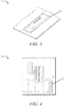
- FIG. 3 illustrates an example single layer 104-2 of material that, when integrated on a circuit board, is configured as a single layer waveguide antenna having channels at least partially defined by the circuit board and filled with air.
- FIG. 4 illustrates an example surface of a circuit board 108-2 configured to act as a floor to channels filled with air for a single layer air waveguide antenna that is integrated on the circuit board.
- dashed line B a single channel with three openings through to an air dielectric is highlighted.
- the single channel highlighted in FIG. 3 aligns with a similarly sized portion of the circuit board 108-2, shown in dashed line B.
- FIG. 5 illustrates another example of a single layer air waveguide antenna 106-3 being integrated on a circuit board 108-3.
- a single layer 104-3 of material is aligned over a portion of the circuit board 108-3, to create an interface 500.
- the interface 500 includes a mechanical as well as an electrical feature. Electrical connections 204-1 are made between the two surfaces.
- a surface of a first layer 104-3 may share the interface 500 with a complementary surface of the circuit board 108-3.
- the interface 500 includes a ball-and-socket type of interface
- the first interface surface may include the balls
- the second interface surface may include the sockets.
- the first and second interface surfaces may include a combination of "balls" and "sockets" as long as they are complimentary between adjacent surfaces. This is the case no matter which interface is used, except in the implementation where the mechanical interface on both interface surfaces is an irregular roughed area. In this implementation, the nature of the irregularity of the roughed surface, along with the layers being compressed together, enables a complementary relation between the two adjacent interface surfaces.
- the mechanical interface on an interface surface may be one complementary interface of one type of mechanical interface, a combination of complementary interfaces of one type of mechanical interface, or any combination of the above and including other types of mechanical interfaces.
- the interface 500 provides a mechanical connection between the two parts of the air waveguide antenna 106-3; lateral movement between the two parts is reduced.
- the resulting interface 500 between the air waveguide antenna 106 and the circuit board 108 may reduce, if not eliminate, a need for solder at their joint. Eliminating the use of soldering techniques to electrically connect and thereby integrate an air waveguide onto a circuit board reduces costs associated with manufacturing. Attaching the air waveguide antenna 106 to the circuit board 108 without using solder presents less risk of causing thermal damage to either the circuit board 108 or the single layer 104 of material (e.g., a metal-coated plastic). These less stringent manufacturing techniques may be easier to achieve, resulting in fewer manufacturing steps performed, and fewer defects, which can reduce costs, particularly when manufactured in large quantities. These example air waveguides may, therefore, be far easier and less expensive to manufacture than existing waveguide technology.
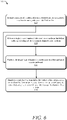
- FIG. 6 illustrates an example process 600 of manufacturing a single layer air waveguide antenna integrated on a circuit board.
- FIG. 6 is described in the context of FIG. 1 ; however, the process 600 can be applied to forming any of the example air waveguide antennas discussed in relation to any of the other drawings.
- the waveguide 106 is one example of a waveguide antenna that may be formed through the process 600, other variations of the waveguide 106 are possible.
- a portion of a surface of a circuit board is identified to act as an electrical interface to waveguide channels filled with air.
- a portion of a surface of the circuit board 108 e.g., an area near an electrical connection to the radar system 102 is configured to operate as a floor 124 of the channels 114 of the waveguide antenna 106 that is being formed through the process 600 and filled with air.
- a single layer of material is obtained with conductive surfaces that define walls and a ceiling of the waveguide channels filled with air.
- the single layer 104 of material e.g., metal, metal-coated plastic
- the single layer 104 includes a surface that defines the ceiling 122 and the walls 120 of the channels 114 being formed through the process 600 and filled with air.
- the single layer of material (i.e., obtained at 604) is positioned atop the portion of the surface of the circuit board 108 (i.e., identified at 602).
- the single layer 104 of material is aligned with the circuit board 108, so when they meet from being joined together, the resulting waveguide antenna 106 includes cavities that define the channels 114, with surfaces of the channels 114 being formed from a combination of the surface of the single layer 104 of material and the surface of the circuit board 108.
- the single layer of material is attached to the portion of the surface of the circuit board to form an air waveguide antenna that is configured to guide electromagnetic energy through the waveguide channels filled with air.
- the joint between the circuit board 108 and the single layer 104 of material is configured as a mechanical interface that prevents separation and further prevents lateral movement.
- the mechanical interface formed at 608 configures the two pieces to be a waveguide antenna device. Cost and material savings can be realized from integrating waveguide technology onto circuit boards using the process 600, when compared to traditional waveguide manufacturing techniques.
- FIGS. 7-12 illustrate different techniques 700 for attaching a single layer of material to a surface of a circuit board to form a single layer air waveguide antenna that is integrated on the circuit board.
- the mechanical interface formed at 602 includes an electrical interface formed from performing the process 600.
- the mechanical connection between the single layer 104 of material and the circuit board 108 can also provide an electrical function, such as enabling an electrical connection (e.g., the electrical connections 204) between the single layer 104 of material and the circuit board 108.
- This electrical connection may include a common potential of the circuit board 108, a connection to an antenna array, or port of a radar chip (e.g., MMIC).
- the attaching performed at 608 of the process 600 includes attaching the single layer of material to the portion of the surface of the circuit board comprises reflow soldering the single layer of material to the circuit board using a low-temperature solder.
- an electrical interface between the single layer 104 of material and the circuit board 108 can be formed using a reflow soldering, including a low-temperature solder (e.g., based on compounds of one or more of argon (Ag), benzyl (Bn), cadmium (Cd), indium (In), lead (Pb), or silicon (Si)) other elements that have a low-temperature melting point in a range of thirty to two-hundred degrees Celsius).
- a low-temperature solder e.g., based on compounds of one or more of argon (Ag), benzyl (Bn), cadmium (Cd), indium (In), lead (Pb), or silicon (Si)
- a high-temperature solder may cause thermal damage to the single layer 104 of material or the circuit board 108, even if precautions are taken.
- a machine controls movement of the two materials during reflow when fixturing and pins are added to the circuit board 108.
- a solder resist may be used to prevent in-solder from leaking into the channels 114. Metal removed from a metalized plastic surface can be used to create a solder resist.
- a pressure-sensitive adhesive 800 is shown that can form the interface between the circuit board 108 and the single layer 104 of material.
- the adhesive 800 may include a double-sided tape.
- FIG. 8 depicts the adhesive 800 as having a release liner 802, as well as a carrier layer 804 sandwiched between two adhesive layers 806.
- FIG. 9 illustrates the adhesive 800 from a different perspective.
- the adhesive 800 can be applied to the single layer 104 of material or the circuit board 108.
- the adhesive can be conductive adhesive or a mixture of conductive and non-conductive materials. The conduction of the adhesive 800 is considered when preparing the single layer 104 of material and the circuit board 108 to ensure conductive materials are used where an electrical interface is needed and allow non-conductive materials to be used for cost or other considerations in areas where a mechanical interface alone is sufficient.
- the adhesive 800 may be a pressure-sensitive adhesive cut to shape and used to adhere the single layer 104 of material to the circuit board 108. Because the adhesive is at least partially filled with conductive particles, it electrically connects the waveguide antenna 106 to the circuit board 108 around the perimeter of the channels 114. In addition, or instead of using the adhesive 800, other adhesives may be dispensed on either the circuit board 108 or the single layer 104 of material to join the two pieces of the waveguide antenna 106.
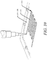
- FIG. 10 depicts a conductive adhesive 1000 that can be dispensed or printed around the perimeter of the channels 114 to ensure adequate electrical connection from the waveguide antenna 106 to the circuit board 108.
- Non-conductive adhesive could be used in other areas to possibly reduce cost.
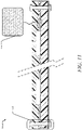
- FIG. 11 illustrates an example air waveguide antenna 106-4.
- FIG. 11 illustrates that attaching the single layer 104 of material to the portion of the surface of the circuit board 108 at 608 of the process 600 may include securing the single layer 104 of material to the circuit board 108 with a mechanical fastener 1002.
- the mechanical fastener 1002 can be a screw, a pin, a bolt, or other component that keeps pressure between the single layer 104 of material and the circuit board 108.
- FIG. 11 illustrates that attaching the single layer 104 of material to the portion of the surface of the circuit board 108 at 608 of the process 600 may include securing the single layer 104 of material to the circuit board 108 by performing a low-pressure sintering of the single layer 104 of material to the circuit board 108.
- the single layer 104 of material to the portion of the surface of the circuit board 108 at 608 of the process 600 may include forming piercing dimples during the molding operation of the single layer 104 of material to form an interface 500-1 located between the channels 114.
- dimples can be formed in an all-metal version of the single layer 104 of material.
- the dimples of the interface 500-1 are then metalized by PVD or plating. The dimples can then be pressed into a solder that has been previously printed and reflowed on the circuit board 108.
- FIG. 11 illustrates that attaching the single layer 104 of material to the portion of the surface of the circuit board 108 at 608 of the process 600 may include securing the single layer 104 of material to the circuit board 108 by performing a reflow soldering of the single layer 104 of material to the circuit board 108.
- the single layer 104 of material to the portion of the surface of the circuit board 108 at 608 of the process 600 may include forming piercing dimples during the molding operation of the single layer 104 of material to form an interface 500-1 located between the channels 114.
- dimples can be formed in an all-metal version of the single layer 104 of material.
- the dimples of the interface 500-1 are then metalized by PVD or plating. The dimples can then be pressed into a solder that has been previously printed and reflowed on the circuit board 108. This technique results in an electrical and mechanical function for the interface 500-1.
- the interfaces 500 or 500-1 can include other features or structures to enable a secure connection between the layer 104 of material and the circuit board 108.
- the pattern of dimples can be replaced with a pattern of teeth, ridges, protrusions, or other features that mate to a corresponding pattern of elements in the circuit board 108.
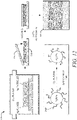
- FIG. 12 illustrates that attaching the single layer 104 of material to the portion of the surface of the circuit board 108 at 608 of the process 600 may include securing the single layer 104 of material to the circuit board 108 by performing a low-pressure sintering of the single layer 104 of material to the circuit board 108.
- the low or no pressure sintering e.g., using Cu, using Ag
- Sintering process temperatures are around two hundred to two hundred and forty degrees Celsius, which requires a silver or copper screen printable sintering material to be used for the single layer 104. Once sintered, the joint can survive over nine hundred degrees Celsius and is not affected by subsequent soldering operations.
- FIG. 13 illustrates that attaching the single layer 104 of material to the portion of the surface of the circuit board 108 at 608 of the process 600 may include securing the single layer 104 of material to the circuit board 108 by performing a hot bar soldering of the single layer 104 of material to the circuit board 108.
- a hot bar tool 1306 is made to fit the topography of the single layer 104 of material.
- Solder 1308 is printed on the circuit board 108.
- the single layer 104 of material is placed onto the circuit board 108, and the hot bar tool 1306 contacts a surface of the single layer 104 of material in response to a pressure 1302 being applied to the hot bar tool 1306, and the hot bar tool 1306 applies heat via an electrical current 1304 to reflow the solder 1308 and create a metallic joint between the circuit board 108 and the resulting waveguide antenna 106.
- Example 1 An apparatus, the apparatus comprising: an air waveguide antenna configured to guide electromagnetic energy through channels filled with air, the air waveguide comprising: an electrical interface to a circuit board, the electrical interface configures a portion of a surface of the circuit board to act as a floor of the channels filled with air; and a single layer of material having conductive surfaces and positioned atop the electrical interface to define walls and a ceiling of the channels filled with air.
- an air waveguide antenna configured to guide electromagnetic energy through channels filled with air
- the air waveguide comprising: an electrical interface to a circuit board, the electrical interface configures a portion of a surface of the circuit board to act as a floor of the channels filled with air; and a single layer of material having conductive surfaces and positioned atop the electrical interface to define walls and a ceiling of the channels filled with air.
- Example 2 The apparatus of any example above or below, wherein the electrical interface to the circuit board comprises a reflow soldering to the circuit board including a low-temperature solder.
- Example 3 The apparatus of any example above or below, wherein the electrical interface to the circuit board comprises a conductive adhesive to the circuit board.
- Example 4 The apparatus of any example above or below, wherein the electrical interface to the circuit board comprises a non-conductive adhesive to the circuit board.
- Example 5 The apparatus of any example above or below, wherein the electrical interface to the circuit board comprises a pressure-sensitive adhesive to the circuit board.
- Example 6 The apparatus of any example above or below, wherein the electrical interface to the circuit board further comprises a mechanical interface to the circuit board.
- Example 7 The apparatus of any example above or below, wherein the mechanical interface to the circuit board comprises a pattern of teeth that mate to a corresponding pattern of teeth in the circuit board.
- Example 8 The apparatus of any example above or below, wherein the electrical interface to the circuit board comprises a low-pressure sintering to the circuit board.
- Example 9 The apparatus of any example above or below, wherein the electrical interface to the circuit board comprises a hot bar soldering to the circuit board.
- Example 10 The apparatus of any example above or below, wherein the floor of the channels filled with air is parallel to the ceiling of the channels filled with air.
- Example 11 The apparatus of any example above or below, wherein the walls of the channels filled with air are orthogonal to the floor of the channels filled with air.
- Example 12 The apparatus of any example above or below, wherein the single layer of material is positioned atop the electrical interface to further define an opening to the channels filled with air, the opening to the channels filled with air comprises a rectangular opening, two sides of the rectangular opening including the walls of the channels filled with air, and two other sides of the rectangular opening including the ceiling and the floor of the channels filled with air.
- Example 13 The apparatus of any example above or below, wherein the single layer of material comprises a non-conductive core and an outer conductive surface.
- Example 14 The apparatus of any example above or below, wherein the non-conductive core comprises plastic and the outer conductive surface comprises metal.
- Example 15 The apparatus of any example above or below, wherein the single layer of material comprises metal.
- Example 16 The apparatus of any example above or below, wherein the ceiling of the channels filled with air comprises one or more slots configured to radiate the electromagnetic energy.
- Example 17 A method, the method comprising: identifying a portion of a surface of a circuit board to act as an electrical interface to waveguide channels filled with air; obtaining a single layer of material with conductive surfaces that define walls and a ceiling of the waveguide channels filled with air; positioning the single layer of material atop the portion of the surface of the circuit board; and attaching the single layer of material to the portion of the surface of the circuit board to form an air waveguide antenna that is configured to guide electromagnetic energy through the waveguide channels filled with air.
- Example 18 The method of any example above or below, wherein attaching the single layer of material to the portion of the surface of the circuit board comprises reflow soldering the single layer of material to the circuit board using a low-temperature solder.
- Example 19 The method of any example above or below, wherein attaching the single layer of material to the portion of the surface of the circuit board comprises applying an adhesive to the single layer of material or the circuit board.
- Example 20 The method of any example above or below, wherein attaching the single layer of material to the portion of the surface of the circuit board comprises securing the single layer of material to the circuit board with a mechanical fastener.
- Example 21 The method of any example above or below, wherein attaching the single layer of material to the portion of the surface of the circuit board comprises performing a low-pressure sintering of the single layer of material to the circuit board.
- Example 22 The method of any example above or below, wherein attaching the single layer of material to the portion of the surface of the circuit board comprises performing a hot bar soldering of the single layer of material to the circuit board.
- Example 23 The method of any example above or below, wherein attaching the single layer of material to the portion of the surface of the circuit board comprises forming a mechanical interface between the single layer of material and the circuit board.
- Example 24 The method of any example above or below, wherein the mechanical interface comprises the electrical interface.
- Example 25 The method of any example above or below, wherein forming the mechanical interface between the single layer of material and the circuit board comprises enabling an electrical connection between the single layer of material and the circuit board.
- Example 26 The method of any example above, wherein the electrical connection comprises a common potential of the circuit board.
- Example 27 A system comprising means for performing the method of any example above.
- Example 28 A system comprising at least one processor configured to control manufacturing equipment to perform the method of any example above.
- Example 29 A computer-readable storage medium comprising instructions that, when executed, cause at least one processor of a system to control manufacturing equipment to perform the method of any example above.
- "at least one of: a, b, or c” is intended to cover a, b, c, a-b, a-c, b-c, and a-b-c, as well as any combination with multiples of the same element (e.g., a-a, a-a-a, a-a-b, a-a-c, a-b-b, a-c-c, b-b, b-b-b, b-b-c, c-c, and c-c-c or any other ordering of a, b, and c).
Landscapes
- Engineering & Computer Science (AREA)
- Manufacturing & Machinery (AREA)
- Computer Security & Cryptography (AREA)
- Radar, Positioning & Navigation (AREA)
- Remote Sensing (AREA)
- Microelectronics & Electronic Packaging (AREA)
- Variable-Direction Aerials And Aerial Arrays (AREA)
Abstract
Description
- Air waveguides are used in many applications, for example, as antennas to shape or filter, based on frequency, an electromagnetic energy beam. Channels filled with air are some of the internal features of an air waveguide. These channels may include openings, referred to as radiators or slots, that allow electromagnetic energy to be filtered in or filtered out. Some waveguide channels may be formed from multiple layers of substrate material, stacked, and soldered together to form walls of a channel. Other air waveguides have been formed using Teflon and FR4 Printed Circuit Board (PCB) materials. Still some other air waveguides are manufactured using injection molded plastics (e.g., filled Polyetherimide (PEI)) that are given a metal coating (e.g., silver). Forming air waveguides using existing manufacturing techniques can be too expensive for some applications, including an automotive context where eventual mass-production is desired.
- This document describes a single-layer air waveguide antenna integrated on a circuit board. In one example, an apparatus includes an air waveguide antenna configured to guide electromagnetic energy through channels filled with air. The air waveguide includes an electrical interface to a circuit board and a single layer of material having conductive surfaces positioned atop the electrical interface. The electrical interface configures a portion of a surface of the circuit board to act as a floor of the channels filled with air. The single layer of material defines walls and a ceiling of the channels filled with air.
- In another example, a method is described. The method includes identifying a portion of a surface of a circuit board to act as an electrical interface to waveguide channels filled with air. The method further includes obtaining a single layer of material with conductive surfaces that define walls and a ceiling of the waveguide channels filled with air, and positioning the single layer of material atop the portion of the surface of the circuit board. The method further includes attaching the single layer of material to the portion of the surface of the circuit board to form an air waveguide antenna that is configured to guide electromagnetic energy through the waveguide channels filled with air.
- This Summary introduces simplified concepts related to a single layer air waveguide that is integrated on a circuit board, as further described in the Detailed Description and Drawings. This Summary is not intended to identify essential features of claimed subject matter, nor is it intended for use in determining the scope of the subject matter claimed.
- The details of one or more aspects of a single-layer air waveguide that is integrated on a circuit board are described in this document with reference to the following figures. The numbers are often used throughout the drawings to reference like features and components:
-
FIG. 1 illustrates an example environment in which a radar system with a single layer air waveguide antenna is integrated on a circuit board that is configured for use on a vehicle; -
FIG. 2 illustrates an example of a single layer air waveguide antenna being integrated on a circuit board; -
FIG. 3 illustrates an example single layer of material that, when integrated on a circuit board, is configured as a single layer waveguide antenna having channels at least partially defined by the circuit board and filled with air; -
FIG. 4 illustrates an example surface of a circuit board configured to act as a floor to channels filled with air for a single layer air waveguide antenna that is integrated on the circuit board; -
FIG. 5 illustrates another example of a single layer air waveguide antenna being integrated on a circuit board; -
FIG. 6 illustrates an example process of manufacturing a single layer air waveguide antenna integrated on a circuit board; and -
FIGS. 7-13 illustrate different techniques for attaching a single layer of material to a surface of a circuit board to form a single layer air waveguide antenna that is integrated on the circuit board. - Radar systems are a sensing technology that some automotive systems rely on to acquire information about the surrounding environment. Radar systems generally use an antenna or a waveguide to direct electromagnetic energy or signals being transmitted or received. Such radar systems may use any combination of antennas and waveguides to provide increased gain and directivity. As the automotive industry increasingly utilizes radar systems in more vehicles, the challenge to reduce costs associated with waveguides for these radar systems becomes a higher priority for manufacturers.
- Air waveguides are used in many applications, for example, as antennas to shape or filter, based on frequency, an electromagnetic energy beam. Channels filled with air are some of the internal features of an air waveguide. These channels may include openings, referred to as radiators or slots, that allow electromagnetic energy to be filtered in or filtered out. Some waveguide channels may be formed from multiple layers of substrate material, stacked, and soldered together to form walls of the channels. Other air waveguides have been formed using Teflon and FR4 Printed Circuit Board (PCB) materials. Still some other air waveguides are manufactured using injection molded plastics (e.g., filled Polyetherimide (PEI)) that are given a metal coating (e.g., silver) under precisely controlled conditions so as to avoid thermal wear. Forming air waveguides using existing manufacturing techniques can be too expensive for some applications, including an automotive context where eventual mass-production is desired. Lower cost, but still high performance, air waveguide antenna technologies that make radar and other sensing technologies affordable are needed, which can improve driving safety.
- This document describes a single-layer air waveguide antenna integrated on a circuit board. The waveguide guides electromagnetic energy through channels filled with air. It is formed from a single layer of material, such as a sheet of metal, metal-coated plastic, or other material with conductive surfaces that is attached to a circuit board. A portion of a surface of the circuit board is configured as a floor of the channels filled with air. This floor forms an electrical interface between the circuit board and the channels filled with air. The single layer of material is positioned atop this electrical interface to define walls and a ceiling of the channels filled with air. The single layer of material can be secured to the circuit board in various ways. The cost of integrating an air waveguide antenna onto a circuit board this way may be less expensive than other waveguide-manufacturing techniques.
- As the example air waveguide antenna can be manufactured by stacking the single-layer material atop the circuit board, the two materials may be held together by a mechanical interface arranged between two adjacent surfaces. The mechanical interface may further include an electrical interface between the upper portion of the air waveguide antenna that is formed from the single layer of material, and the lower portion of the air waveguide antenna that is formed from the circuit board. The circuit board may include one or more electrical contacts that align with the channels of the air waveguide antenna so that the mechanical interface also electrically couples the two layers. This interface may eliminate a need for solder between connections that can be made directly through the interface formed between the two materials.
- Because there may no longer be a need for using solder to attach the air waveguide antenna to the circuit board, there may be less risk of causing thermal damage to either the circuit board or the single layer of material (e.g., a metal-coated plastic). These less stringent manufacturing requirements may be easier to achieve, resulting in fewer manufacturing steps performed, and fewer defects, which can reduce costs, particularly when manufactured in large quantities. The example air waveguide may, therefore, be far easier and less expensive to manufacture than existing waveguide technology.
-
FIG. 1 illustrates anexample environment 100 in which aradar system 102 with asingle layer 104air waveguide antenna 106 is integrated on acircuit board 108 and configured for use on avehicle 110. Thevehicle 110 may use one or moreair waveguide antennas 106 to enable operations of theradar system 102. For example, responsive to receiving, from theradar system 102, radar data indicative of a position of anobject 112 relative a position of thevehicle 110, thevehicle 110 performs a driving-maneuver to avoid a collision with theobject 112. - Although illustrated as a car, the
vehicle 110 can represent other types of motorized vehicles (e.g., a motorcycle, a bus, a tractor, a semi-trailer truck, or construction equipment), non-motorized vehicles (e.g., a bicycle), railed vehicles (e.g., a train or a trolley car), watercraft (e.g., a boat or a ship), aircraft (e.g., an airplane or a helicopter), or spacecraft (e.g., satellite). In general, manufacturers can mount theradar system 102 to any moving platform, including moving machinery or robotic equipment. In other implementations, other devices (e.g., desktop computers, tablets, laptops, televisions, computing watches, smartphones, gaming systems, and so forth) may incorporate theradar system 102 with theair waveguide antenna 106 and support techniques described herein. - The
radar system 102 can be part of thevehicle 110. In the depictedenvironment 100, theradar system 102 is mounted near, or integrated within, a front portion of thevehicle 110 to detect theobject 112 and avoid collisions. Theradar system 102 provides a field-of-view 118 towards theobject 112. Theradar system 102 can project the field-of-view 118 from any exterior surface of thevehicle 110. For example, vehicle manufacturers can integrate theradar system 102 into a bumper, side mirror, headlights, rear lights, or any other interior or exterior location where theobject 112 requires detection. In some cases, thevehicle 110 includesmultiple radar systems 102, such as afirst radar system 102 and asecond radar system 102 that provide a larger field-of-view 118. In general, vehicle manufacturers can design the locations of the one ormore radar systems 102 to provide a particular field-of-view 118 that encompasses a region of interest, including, for instance, in or around a travel lane aligned with a vehicle path. - The
vehicle 110 can also include at least one automotive system that relies on data from theradar system 102, including a driver-assistance system, an autonomous-driving system, or a semi-autonomous-driving system. Theradar system 102 can include an interface to such automotive systems. A signal can be output, via the interface, based on electromagnetic energy received by theradar system 102. Generally, the automotive systems use radar data provided by theradar system 102 to perform a function. For example, the driver-assistance system can provide blind-spot monitoring and generate an alert indicating a potential collision with theobject 112 detected by theradar system 102. In this case, the radar data from theradar system 102 indicate when it is safe or unsafe to change lanes. The autonomous-driving system may move thevehicle 110 to a particular location on the road while avoiding collisions with theobject 112 detected by theradar system 102. The radar data provided by theradar system 102 can provide information about a distance to and the location of theobject 112 to enable the autonomous-driving system to perform emergency braking, perform a lane change, or adjust the speed of thevehicle 110. - The
radar system 102 generally includes a transmitter (not illustrated) and at least one antenna, including theair waveguide antenna 106, to transmit electromagnetic signals. Theradar system 102 generally includes a receiver (not illustrated) and at least one antenna, including theair waveguide antenna 106, to receive reflected versions of these electromagnetic signals. The transmitter includes components for emitting electromagnetic signals. The receiver includes components to detect the reflected electromagnetic signals. The transmitter and the receiver can be incorporated together on the same integrated circuit (e.g., a transceiver integrated circuit) or separately on different integrated circuits. Theradar system 102 also includes one or more processors (not illustrated) and computer-readable storage media (CRM) (not illustrated). The processor can be a microprocessor or a system-on-chip. The processor executes instructions stored within the CRM. As an example, the processor can control the operation of the transmitter. The processor can also process electromagnetic energy received by theair waveguide antenna 106 and determine the location of theobject 112 relative to theradar system 102. The processor can also generate radar data for the automotive systems. For example, the processor can control, based on processed electromagnetic energy from theair waveguide antenna 106, an autonomous or semi-autonomous driving system of thevehicle 110. - Because forming air waveguide antennas from multiple layers of substrate material, as well as forming air waveguide antennas from stacking substrates and soldering injection-molded plastics, can be too expensive for some applications, including an automotive context where eventual mass-production is desired, the
air waveguide antenna 106 consists of just two main parts. - A first main part consists of a metal or metalized-
plastic layer 104 defining openings 116 (e.g., ports and radiators) intochannels 114 that are filled with a dielectric, which in this example is air. Thechannels 114 are partially surrounded byvertical walls 120 and aceiling 122. The purpose of thechannels 114 is to guide desirable electromagnetic energy that is captured by theair waveguide antenna 106 to or from other components of the radar system 102 (e.g., a transceiver). - A second main part of the
air waveguide antenna 106 consists of a portion of the circuit board 108 (e.g., a substrate or other circuit board). Thesingle layer 104 is integrated on and attached to thecircuit board 108 so as to define thechannels 114 that contain the dielectric (e.g., air). Thevertical walls 120 that form thechannels 114 within the first main part of theair waveguide antenna 106 are mated to a surface of thecircuit board 108 that is configured to define afloor 124 of thechannels 114. Thefloor 124 is arranged opposite (e.g., substantially parallel to) the ceiling 12. When the two main parts are put together, they create an electrical connection between theair waveguide antenna 106 and other components of theradar system 102. - The
single layer 104 can be formed of a single sheet of metal that is stamped or bent to take on a particular shape. Thesingle layer 104 may consist of a metalized plastic; a surface coating of metal material may be applied to an injection-molded or printed plastic part that is at the desired shape. Thesingle layer 104 of material may include a non-conductive core and an outer conductive surface. For example, the non-conductive core of thesingle layer 104 of material may include plastic and the outer conductive surface may include metal. - As shown in
FIG. 1 , theair waveguide antenna 106 includes twochannels 114. Generally, thechannels 114 define a rectangular cavity surrounded by threevertical walls 120 with an opening at one end. Thechannels 114 and theopenings 116 manipulate the electromagnetic energy in a manner that is advantageous for a particular application of theair waveguide antenna 106. Thevertical walls 120 of the channels 114 (e.g., surfaces of thechannels 114 that are perpendicular relative to the flow of electromagnetic energy that passes through the channels 114) guide the electromagnetic energy in a lateral direction across a surface of thecircuit board 108. Theceiling 122 and thefloor 124 of the channels 114 (e.g., surfaces that are parallel to the flow of electromagnetic energy that passes through the channels) regulate, in a perpendicular direction, in-flow and out-flow of the electromagnetic energy through theopenings 116. - For example, the
single layer 104 includes theopenings 116 through theceiling 122 and into thechannels 114, which permit undesirable electromagnetic energy (e.g., energy that is outside an operating frequency) to escape theair waveguide 106, and which allow desirable electromagnetic energy (e.g., energy that is inside the operating frequency) to flow within theair waveguide 106. Theopenings 116 allow electromagnetic energy to enter the channels 114 (e.g., acting as ports) and exit the channels 114 (e.g., acting as radiators or slots). - The
floor 124 of thechannels 114, which is provided by thecircuit board 108, prevents electromagnetic energy that passes through thechannels 114 from escaping theair waveguide 106 through thecircuit board 108. Thefloor 124 of thechannels 114 is formed by an exterior surface of thecircuit board 108 that is in contact with thevertical walls 120 of thesingle layer 104. Although not shown inFIG. 1 , thefloor 124 of thechannels 114 may include a connection to a wire, a pad, or a trace that electrically couples theair waveguide antenna 106 to other components of theradar system 102, for instance, other components (not shown) that are integrated on or otherwise attached to thecircuit board 108. Positioned opposite thecircuit board 108, theceiling 122 of the channels 114 (e.g., surfaces that are parallel to the flow of electromagnetic energy that passes through the channels) regulates in-flow and out-flow of the electromagnetic energy above thecircuit board 108 and through the throughopenings 116. - The
layer 104 can be any solid material, including wood, carbon fiber, fiberglass, metal, plastic, or a combination thereof. One common material used for thelayer 104 is injection molded plastics (e.g., filled PEI). Thelayer 104 may be metalized (e.g., coated via plating, physical vapor deposition, painting, or other forms of metallization). The metal used to metalize thelayer 104 may be silver, silver alloy, copper, aluminum, cold-rolled steel, stainless steel, or other conductive metal. - The
layer 104 shares aninterface 126 to thecircuit board 108. Theinterface 126 provides a mechanical joint between the two materials. In addition, theinterface 126 can provide an electrical function. Theinterface 126 may be referred to as an electrically connecting layer. - The
air waveguide antenna 106 can be manufactured by stacking thesingle layer 104 atop thecircuit board 108. The two materials may be held together by theinterface 126, which is configured as a mechanical interface arranged between two adjacent surfaces, in addition to being configured as an electrical interface between the two pieces, as well. - With regards to the mechanical interface provided by the
interface 126, in some examples, theinterface 126 includes a friction joint formed by external pressure placed around the two adjacent surfaces (e.g., using claps, screws, other fasteners). Theinterface 126 may include a pattern of mechanical features (e.g., protrusions, dimples, bumps, teeth, blocks, snap-fasteners, ball-and-sockets, reciprocal-roughed-surfaces) on one or both of the adjacent surfaces such that, when held together under pressure, the features cause a bond that restricts lateral movement and, therefore, maintains vertical alignment, between the two materials. In some cases, theinterface 126 between the two air waveguide pieces includes an adhesive joint, a taped-joint, a soldered joint, a weld, a reflow-soldered joint with low-temperature solder, a dispensed conductive or non-conductive adhesive joint, a pressure-sensitive adhesive, a low-pressure sintered-joint, a hot-bar soldered joint, or other type of connection. - The
interface 126 may further include an electrical coupling, or electrical interface, between the upper portion of theair waveguide antenna 106 that is formed from thesingle layer 104 of material, and the lower portion of theair waveguide antenna 106 that is formed from thecircuit board 108. - Although not shown in
FIG. 1 , thecircuit board 108 may include one or more electrical contacts that align with thechannels 114 of theair waveguide antenna 106 so that theinterface 126 also electrically couples the two materials. For example, an input or output of a transceiver or other component of theradar system 102 may be electrically coupled to theair waveguide antenna 106 through theinterface 126 with thecircuit board 108. As another example, theinterface 126 may electrically couple theair waveguide antenna 106 to a common potential of theradar system 102. Thisinterface 126 may eliminate a need for solder between connections that can instead be made directly through theinterface 126. - The
single layer 104 of material can be structurally secured to thecircuit board 108 and electrically coupled to thecircuit board 108 in various ways, as described in greater detail below. Generally, theinterface 126 enables an inexpensive manufacturing process for theair waveguide antenna 106 without the need for solder to physically connect and electrically couple thelayer 104 to thecircuit board 108. Using the relatively inexpensiveair waveguide antenna 106 for radar applications invehicles 110 may ultimately contribute to greater adoption of advanced safety technology in vehicles, which may improve driving safety. -
FIG. 2 illustrates an example of a single layer 104-1 of an air waveguide antenna 106-1 being integrated on a circuit board 108-1. The air waveguide antenna 106-1 is an example of theair waveguide antenna 106. - In the top-right corner of
FIG. 2 , the air waveguide antenna 106-1 is shown in assembled form. The rest ofFIG. 2 shows the air waveguide antenna 106-1 with a partial cut-out A to aid in explanation. - The layer 104-1 is aligned atop of a
surface 200 of the circuit board 108-1 so thatportions 202 of thesurface 200 are configured as a floor 124-1 to one or more channels 114-1. Walls 120-1 and a ceiling 122-1 of the channels 114-1 are defined by the layer 104-1 of material. The ceiling 122-1 includes openings 116-1 for radiating or absorbing energy. - Also shown in
FIG. 2 are example electrical connections 204 (e.g., traces, pads, terminals, pins, wires) to the circuit board 108-1. The channels 114-1 defined by the layer 104-1 can be aligned to theelectrical connections 204. Other parts of the air waveguide antenna 106-1, for instance, material of the layer 104-1 that is between the channels 114-1, may include an electrical interface through theelectrical connections 204, for example, to set theair waveguide 106 to a common potential. -
FIG. 3 illustrates an example single layer 104-2 of material that, when integrated on a circuit board, is configured as a single layer waveguide antenna having channels at least partially defined by the circuit board and filled with air.FIG. 4 illustrates an example surface of a circuit board 108-2 configured to act as a floor to channels filled with air for a single layer air waveguide antenna that is integrated on the circuit board. As dashed line B, a single channel with three openings through to an air dielectric is highlighted. When viewed with reference toFIG. 4 , the single channel highlighted inFIG. 3 aligns with a similarly sized portion of the circuit board 108-2, shown in dashed line B. -
FIG. 5 illustrates another example of a single layer air waveguide antenna 106-3 being integrated on a circuit board 108-3. A single layer 104-3 of material is aligned over a portion of the circuit board 108-3, to create aninterface 500. When the two main parts of the air waveguide antenna 106-3 are brought together as shown, theinterface 500 includes a mechanical as well as an electrical feature. Electrical connections 204-1 are made between the two surfaces. - A surface of a first layer 104-3 may share the
interface 500 with a complementary surface of the circuit board 108-3. For example, if theinterface 500 includes a ball-and-socket type of interface, then the first interface surface may include the balls, and the second interface surface may include the sockets. Alternatively, the first and second interface surfaces may include a combination of "balls" and "sockets" as long as they are complimentary between adjacent surfaces. This is the case no matter which interface is used, except in the implementation where the mechanical interface on both interface surfaces is an irregular roughed area. In this implementation, the nature of the irregularity of the roughed surface, along with the layers being compressed together, enables a complementary relation between the two adjacent interface surfaces. The mechanical interface on an interface surface may be one complementary interface of one type of mechanical interface, a combination of complementary interfaces of one type of mechanical interface, or any combination of the above and including other types of mechanical interfaces. Theinterface 500 provides a mechanical connection between the two parts of the air waveguide antenna 106-3; lateral movement between the two parts is reduced. - The resulting
interface 500 between theair waveguide antenna 106 and thecircuit board 108 may reduce, if not eliminate, a need for solder at their joint. Eliminating the use of soldering techniques to electrically connect and thereby integrate an air waveguide onto a circuit board reduces costs associated with manufacturing. Attaching theair waveguide antenna 106 to thecircuit board 108 without using solder presents less risk of causing thermal damage to either thecircuit board 108 or thesingle layer 104 of material (e.g., a metal-coated plastic). These less stringent manufacturing techniques may be easier to achieve, resulting in fewer manufacturing steps performed, and fewer defects, which can reduce costs, particularly when manufactured in large quantities. These example air waveguides may, therefore, be far easier and less expensive to manufacture than existing waveguide technology. -
FIG. 6 illustrates anexample process 600 of manufacturing a single layer air waveguide antenna integrated on a circuit board.FIG. 6 is described in the context ofFIG. 1 ; however, theprocess 600 can be applied to forming any of the example air waveguide antennas discussed in relation to any of the other drawings. In other words, although thewaveguide 106 is one example of a waveguide antenna that may be formed through theprocess 600, other variations of thewaveguide 106 are possible. - At 602, a portion of a surface of a circuit board is identified to act as an electrical interface to waveguide channels filled with air. For example, a portion of a surface of the circuit board 108 (e.g., an area near an electrical connection to the radar system 102) is configured to operate as a
floor 124 of thechannels 114 of thewaveguide antenna 106 that is being formed through theprocess 600 and filled with air. - At 604, a single layer of material is obtained with conductive surfaces that define walls and a ceiling of the waveguide channels filled with air. For example, the
single layer 104 of material (e.g., metal, metal-coated plastic) can be created through injection molding techniques, or through other fabrication processes, including bending and shaping of sheet metal alone or in combination with precision cutting techniques. Thesingle layer 104 includes a surface that defines theceiling 122 and thewalls 120 of thechannels 114 being formed through theprocess 600 and filled with air. - At 606, the single layer of material (i.e., obtained at 604) is positioned atop the portion of the surface of the circuit board 108 (i.e., identified at 602). For example, the
single layer 104 of material is aligned with thecircuit board 108, so when they meet from being joined together, the resultingwaveguide antenna 106 includes cavities that define thechannels 114, with surfaces of thechannels 114 being formed from a combination of the surface of thesingle layer 104 of material and the surface of thecircuit board 108. - At 608, the single layer of material is attached to the portion of the surface of the circuit board to form an air waveguide antenna that is configured to guide electromagnetic energy through the waveguide channels filled with air. For example, using one or more of the techniques depicted in
FIGS. 7-13 , the joint between thecircuit board 108 and thesingle layer 104 of material is configured as a mechanical interface that prevents separation and further prevents lateral movement. The mechanical interface formed at 608 configures the two pieces to be a waveguide antenna device. Cost and material savings can be realized from integrating waveguide technology onto circuit boards using theprocess 600, when compared to traditional waveguide manufacturing techniques.FIGS. 7-12 illustratedifferent techniques 700 for attaching a single layer of material to a surface of a circuit board to form a single layer air waveguide antenna that is integrated on the circuit board. - In many cases, the mechanical interface formed at 602 includes an electrical interface formed from performing the
process 600. For example, the mechanical connection between thesingle layer 104 of material and thecircuit board 108 can also provide an electrical function, such as enabling an electrical connection (e.g., the electrical connections 204) between thesingle layer 104 of material and thecircuit board 108. This electrical connection may include a common potential of thecircuit board 108, a connection to an antenna array, or port of a radar chip (e.g., MMIC). - In
FIG. 7 , the attaching performed at 608 of theprocess 600 includes attaching the single layer of material to the portion of the surface of the circuit board comprises reflow soldering the single layer of material to the circuit board using a low-temperature solder. As shown inFIG. 7 , an electrical interface between thesingle layer 104 of material and thecircuit board 108 can be formed using a reflow soldering, including a low-temperature solder (e.g., based on compounds of one or more of argon (Ag), benzyl (Bn), cadmium (Cd), indium (In), lead (Pb), or silicon (Si)) other elements that have a low-temperature melting point in a range of thirty to two-hundred degrees Celsius). Using a high-temperature solder may cause thermal damage to thesingle layer 104 of material or thecircuit board 108, even if precautions are taken. When performing low-temperature soldering, a machine controls movement of the two materials during reflow when fixturing and pins are added to thecircuit board 108. To prevent portions of the low-temperature solder from acting as in-solder, a solder resist may be used to prevent in-solder from leaking into thechannels 114. Metal removed from a metalized plastic surface can be used to create a solder resist. - In
FIGS. 8 and 9 , a pressure-sensitive adhesive 800 is shown that can form the interface between thecircuit board 108 and thesingle layer 104 of material. The adhesive 800 may include a double-sided tape.FIG. 8 depicts the adhesive 800 as having arelease liner 802, as well as acarrier layer 804 sandwiched between twoadhesive layers 806.FIG. 9 illustrates the adhesive 800 from a different perspective. - The adhesive 800 can be applied to the
single layer 104 of material or thecircuit board 108. The adhesive can be conductive adhesive or a mixture of conductive and non-conductive materials. The conduction of the adhesive 800 is considered when preparing thesingle layer 104 of material and thecircuit board 108 to ensure conductive materials are used where an electrical interface is needed and allow non-conductive materials to be used for cost or other considerations in areas where a mechanical interface alone is sufficient. The adhesive 800 may be a pressure-sensitive adhesive cut to shape and used to adhere thesingle layer 104 of material to thecircuit board 108. Because the adhesive is at least partially filled with conductive particles, it electrically connects thewaveguide antenna 106 to thecircuit board 108 around the perimeter of thechannels 114. In addition, or instead of using the adhesive 800, other adhesives may be dispensed on either thecircuit board 108 or thesingle layer 104 of material to join the two pieces of thewaveguide antenna 106. -
FIG. 10 depicts a conductive adhesive 1000 that can be dispensed or printed around the perimeter of thechannels 114 to ensure adequate electrical connection from thewaveguide antenna 106 to thecircuit board 108. Non-conductive adhesive could be used in other areas to possibly reduce cost. -
FIG. 11 illustrates an example air waveguide antenna 106-4.FIG. 11 illustrates that attaching thesingle layer 104 of material to the portion of the surface of thecircuit board 108 at 608 of theprocess 600 may include securing thesingle layer 104 of material to thecircuit board 108 with amechanical fastener 1002. Themechanical fastener 1002 can be a screw, a pin, a bolt, or other component that keeps pressure between thesingle layer 104 of material and thecircuit board 108. -
FIG. 11 illustrates that attaching thesingle layer 104 of material to the portion of the surface of thecircuit board 108 at 608 of theprocess 600 may include securing thesingle layer 104 of material to thecircuit board 108 by performing a low-pressure sintering of thesingle layer 104 of material to thecircuit board 108. Thesingle layer 104 of material to the portion of the surface of thecircuit board 108 at 608 of theprocess 600 may include forming piercing dimples during the molding operation of thesingle layer 104 of material to form an interface 500-1 located between thechannels 114. Similarly, dimples can be formed in an all-metal version of thesingle layer 104 of material. The dimples of the interface 500-1 are then metalized by PVD or plating. The dimples can then be pressed into a solder that has been previously printed and reflowed on thecircuit board 108. -
FIG. 11 illustrates that attaching thesingle layer 104 of material to the portion of the surface of thecircuit board 108 at 608 of theprocess 600 may include securing thesingle layer 104 of material to thecircuit board 108 by performing a reflow soldering of thesingle layer 104 of material to thecircuit board 108. Thesingle layer 104 of material to the portion of the surface of thecircuit board 108 at 608 of theprocess 600 may include forming piercing dimples during the molding operation of thesingle layer 104 of material to form an interface 500-1 located between thechannels 114. Similarly, dimples can be formed in an all-metal version of thesingle layer 104 of material. The dimples of the interface 500-1 are then metalized by PVD or plating. The dimples can then be pressed into a solder that has been previously printed and reflowed on thecircuit board 108. This technique results in an electrical and mechanical function for the interface 500-1. - Although not shown, the
interfaces 500 or 500-1 can include other features or structures to enable a secure connection between thelayer 104 of material and thecircuit board 108. For example, the pattern of dimples can be replaced with a pattern of teeth, ridges, protrusions, or other features that mate to a corresponding pattern of elements in thecircuit board 108. -
FIG. 12 illustrates that attaching thesingle layer 104 of material to the portion of the surface of thecircuit board 108 at 608 of theprocess 600 may include securing thesingle layer 104 of material to thecircuit board 108 by performing a low-pressure sintering of thesingle layer 104 of material to thecircuit board 108. The low or no pressure sintering (e.g., using Cu, using Ag) can be used to electrically attach thesingle layer 104 of material to thecircuit board 108. Sintering process temperatures are around two hundred to two hundred and forty degrees Celsius, which requires a silver or copper screen printable sintering material to be used for thesingle layer 104. Once sintered, the joint can survive over nine hundred degrees Celsius and is not affected by subsequent soldering operations. -
FIG. 13 illustrates that attaching thesingle layer 104 of material to the portion of the surface of thecircuit board 108 at 608 of theprocess 600 may include securing thesingle layer 104 of material to thecircuit board 108 by performing a hot bar soldering of thesingle layer 104 of material to thecircuit board 108. Ahot bar tool 1306 is made to fit the topography of thesingle layer 104 of material.Solder 1308 is printed on thecircuit board 108. Thesingle layer 104 of material is placed onto thecircuit board 108, and thehot bar tool 1306 contacts a surface of thesingle layer 104 of material in response to apressure 1302 being applied to thehot bar tool 1306, and thehot bar tool 1306 applies heat via an electrical current 1304 to reflow thesolder 1308 and create a metallic joint between thecircuit board 108 and the resultingwaveguide antenna 106. - The following are some additional examples that can be considered apart or in combination with any of the examples described above to form single layer air waveguide antennas that are integrated on circuit boards.
- Example 1. An apparatus, the apparatus comprising: an air waveguide antenna configured to guide electromagnetic energy through channels filled with air, the air waveguide comprising: an electrical interface to a circuit board, the electrical interface configures a portion of a surface of the circuit board to act as a floor of the channels filled with air; and a single layer of material having conductive surfaces and positioned atop the electrical interface to define walls and a ceiling of the channels filled with air.
- Example 2. The apparatus of any example above or below, wherein the electrical interface to the circuit board comprises a reflow soldering to the circuit board including a low-temperature solder.
- Example 3. The apparatus of any example above or below, wherein the electrical interface to the circuit board comprises a conductive adhesive to the circuit board.
- Example 4. The apparatus of any example above or below, wherein the electrical interface to the circuit board comprises a non-conductive adhesive to the circuit board.
- Example 5. The apparatus of any example above or below, wherein the electrical interface to the circuit board comprises a pressure-sensitive adhesive to the circuit board.
- Example 6. The apparatus of any example above or below, wherein the electrical interface to the circuit board further comprises a mechanical interface to the circuit board.
- Example 7. The apparatus of any example above or below, wherein the mechanical interface to the circuit board comprises a pattern of teeth that mate to a corresponding pattern of teeth in the circuit board.
- Example 8. The apparatus of any example above or below, wherein the electrical interface to the circuit board comprises a low-pressure sintering to the circuit board.
- Example 9. The apparatus of any example above or below, wherein the electrical interface to the circuit board comprises a hot bar soldering to the circuit board.
- Example 10. The apparatus of any example above or below, wherein the floor of the channels filled with air is parallel to the ceiling of the channels filled with air.
- Example 11. The apparatus of any example above or below, wherein the walls of the channels filled with air are orthogonal to the floor of the channels filled with air.
- Example 12. The apparatus of any example above or below, wherein the single layer of material is positioned atop the electrical interface to further define an opening to the channels filled with air, the opening to the channels filled with air comprises a rectangular opening, two sides of the rectangular opening including the walls of the channels filled with air, and two other sides of the rectangular opening including the ceiling and the floor of the channels filled with air.
- Example 13. The apparatus of any example above or below, wherein the single layer of material comprises a non-conductive core and an outer conductive surface.
- Example 14. The apparatus of any example above or below, wherein the non-conductive core comprises plastic and the outer conductive surface comprises metal.
- Example 15. The apparatus of any example above or below, wherein the single layer of material comprises metal.
- Example 16. The apparatus of any example above or below, wherein the ceiling of the channels filled with air comprises one or more slots configured to radiate the electromagnetic energy.
- Example 17. A method, the method comprising: identifying a portion of a surface of a circuit board to act as an electrical interface to waveguide channels filled with air; obtaining a single layer of material with conductive surfaces that define walls and a ceiling of the waveguide channels filled with air; positioning the single layer of material atop the portion of the surface of the circuit board; and attaching the single layer of material to the portion of the surface of the circuit board to form an air waveguide antenna that is configured to guide electromagnetic energy through the waveguide channels filled with air.
- Example 18. The method of any example above or below, wherein attaching the single layer of material to the portion of the surface of the circuit board comprises reflow soldering the single layer of material to the circuit board using a low-temperature solder.
- Example 19. The method of any example above or below, wherein attaching the single layer of material to the portion of the surface of the circuit board comprises applying an adhesive to the single layer of material or the circuit board.
- Example 20. The method of any example above or below, wherein attaching the single layer of material to the portion of the surface of the circuit board comprises securing the single layer of material to the circuit board with a mechanical fastener.
- Example 21. The method of any example above or below, wherein attaching the single layer of material to the portion of the surface of the circuit board comprises performing a low-pressure sintering of the single layer of material to the circuit board.
- Example 22. The method of any example above or below, wherein attaching the single layer of material to the portion of the surface of the circuit board comprises performing a hot bar soldering of the single layer of material to the circuit board.
- Example 23. The method of any example above or below, wherein attaching the single layer of material to the portion of the surface of the circuit board comprises forming a mechanical interface between the single layer of material and the circuit board.
- Example 24. The method of any example above or below, wherein the mechanical interface comprises the electrical interface.
- Example 25. The method of any example above or below, wherein forming the mechanical interface between the single layer of material and the circuit board comprises enabling an electrical connection between the single layer of material and the circuit board.
- Example 26. The method of any example above, wherein the electrical connection comprises a common potential of the circuit board.
- Example 27. A system comprising means for performing the method of any example above.
- Example 28. A system comprising at least one processor configured to control manufacturing equipment to perform the method of any example above.
- Example 29. A computer-readable storage medium comprising instructions that, when executed, cause at least one processor of a system to control manufacturing equipment to perform the method of any example above.
- While various embodiments of the disclosure are described in the foregoing description and shown in the drawings, it is to be understood that this disclosure is not limited thereto but may be variously embodied to practice within the scope of the following claims. From the foregoing description, it will be apparent that various changes may be made without departing from the scope of the disclosure as defined by the following claims. In addition to radar systems, problems associated with signal attenuation can occur in other radio frequency (RF) systems. Therefore, although described as a way to improve radar antennas and air waveguide antennas for vehicle systems, the techniques of the foregoing description can be applied outside a vehicle context.
- The use of "or" and grammatically related terms indicates non-exclusive alternatives without limitation unless the context clearly dictates otherwise. As used herein, a phrase referring to "at least one of' a list of items refers to any combination of those items, including single members. As an example, "at least one of: a, b, or c" is intended to cover a, b, c, a-b, a-c, b-c, and a-b-c, as well as any combination with multiples of the same element (e.g., a-a, a-a-a, a-a-b, a-a-c, a-b-b, a-c-c, b-b, b-b-b, b-b-c, c-c, and c-c-c or any other ordering of a, b, and c).
Claims (15)
- A method, the method comprising:identifying a portion of a surface of a circuit board to act as an electrical interface to waveguide channels filled with air;obtaining a single layer of material with conductive surfaces that define walls and a ceiling of the waveguide channels filled with air;positioning the single layer of material atop the portion of the surface of the circuit board; andattaching the single layer of material to the portion of the surface of the circuit board to form an air waveguide antenna that is configured to guide electromagnetic energy through the waveguide channels filled with air.
- The method of claim 1, wherein attaching the single layer of material to the portion of the surface of the circuit board comprises one or more of:reflow soldering the single layer of material to the circuit board using a low-temperature solder;applying an adhesive to the single layer of material or the circuit board;securing the single layer of material to the circuit board with a mechanical fastener;performing a low-pressure sintering of the single layer of material to the circuit board; orperforming a hot bar soldering of the single layer of material to the circuit board.
- The method of any preceding claim, wherein attaching the single layer of material to the portion of the surface of the circuit board comprises forming a mechanical interface between the single layer of material and the circuit board, the mechanical interface enabling an electrical connection of the between the single layer of material and the circuit board.
- The method of any preceding claim, wherein the electrical connection comprises a common potential of the circuit board.
- The method of any preceding claim, wherein the electrical interface to the circuit board comprises at least one of:a reflow soldering to the circuit board including a low-temperature solder;a conductive adhesive to the circuit board;a non-conductive adhesive to the circuit board; ora pressure-sensitive adhesive to the circuit board.
- The method of any preceding claim, wherein the electrical interface to the circuit board further comprises a mechanical interface to the circuit board.
- The method of claim 6, wherein the mechanical interface to the circuit board comprises a pattern of teeth that mate to a corresponding pattern of teeth in the circuit board.
- The method of any preceding claim, wherein the electrical interface to the circuit board comprises at least one of:a low-pressure sintering to the circuit board; ora hot bar soldering to the circuit board.
- The method of any preceding claim, wherein the floor of the channels filled with air is parallel to the ceiling of the channels filled with air, and the walls of the channels filled with air are orthogonal to the floor of the channels filled with air.
- The method of any preceding claim, wherein the single layer of material is positioned atop the electrical interface to further define an opening to the channels filled with air, the opening to the channels filled with air comprises a rectangular opening, two sides of the rectangular opening including the walls of the channels filled with air, and two other sides of the rectangular opening including the ceiling and the floor of the channels filled with air.
- The method of any preceding claim, wherein the single layer of material comprises a non-conductive core and an outer conductive surface.
- The method of any preceding claim, wherein the non-conductive core comprises plastic and the outer conductive surface comprises metal.
- The method of any preceding claim, wherein the single layer of material comprises metal.
- The method of any preceding claim, wherein the ceiling of the channels filled with air comprises one or more slots configured to radiate the electromagnetic energy.
- A system comprising:a circuit card; andan air waveguide antenna configured to guide electromagnetic energy through channels filled with air, the air waveguide comprising:an electrical interface to the circuit board, the electrical interface configures a portion of a surface of the circuit board to act as a floor of the channels filled with air; anda single layer of material having conductive surfaces and positioned atop the electrical interface to define walls and a ceiling of the channels filled with air.
Applications Claiming Priority (4)
| Application Number | Priority Date | Filing Date | Title |
|---|---|---|---|
| US202163164368P | 2021-03-22 | 2021-03-22 | |
| US202163170145P | 2021-04-02 | 2021-04-02 | |
| US202163193538P | 2021-05-26 | 2021-05-26 | |
| US17/353,595 US11616306B2 (en) | 2021-03-22 | 2021-06-21 | Apparatus, method and system comprising an air waveguide antenna having a single layer material with air channels therein which is interfaced with a circuit board |
Publications (1)
| Publication Number | Publication Date |
|---|---|
| EP4064457A1 true EP4064457A1 (en) | 2022-09-28 |
Family
ID=80595570
Family Applications (1)
| Application Number | Title | Priority Date | Filing Date |
|---|---|---|---|
| EP22159217.3A Pending EP4064457A1 (en) | 2021-03-22 | 2022-02-28 | Single-layer air waveguide antenna integrated on circuit board |
Country Status (3)
| Country | Link |
|---|---|
| US (2) | US11616306B2 (en) |
| EP (1) | EP4064457A1 (en) |
| CN (2) | CN115117610B (en) |
Families Citing this family (12)
| Publication number | Priority date | Publication date | Assignee | Title |
|---|---|---|---|---|
| US11616306B2 (en) * | 2021-03-22 | 2023-03-28 | Aptiv Technologies Limited | Apparatus, method and system comprising an air waveguide antenna having a single layer material with air channels therein which is interfaced with a circuit board |
| EP4084222A1 (en) | 2021-04-30 | 2022-11-02 | Aptiv Technologies Limited | Dielectric loaded waveguide for low loss signal distributions and small form factor antennas |
| DE102021207896A1 (en) * | 2021-07-22 | 2023-01-26 | Robert Bosch Gesellschaft mit beschränkter Haftung | Radar sensor with waveguide structure |
| US12224502B2 (en) | 2021-10-14 | 2025-02-11 | Aptiv Technologies AG | Antenna-to-printed circuit board transition |
| DE102022202140A1 (en) * | 2022-03-02 | 2023-09-07 | Robert Bosch Gesellschaft mit beschränkter Haftung | Radar device and method of manufacturing a radar device |
| US12265172B2 (en) | 2022-05-25 | 2025-04-01 | Aptiv Technologies AG | Vertical microstrip-to-waveguide transition |
| US12424767B2 (en) | 2022-11-15 | 2025-09-23 | Aptiv Technologies AG | Planar surface features for waveguide and antenna |
| US12506272B2 (en) | 2023-05-16 | 2025-12-23 | Aptiv Technologies AG | Production-tolerant multi-part antenna system |
| TWI869009B (en) * | 2023-10-27 | 2025-01-01 | 大陸商宏恆勝電子科技(淮安)有限公司 | Circuit board and manufacturing method thereof |
| EP4568012A1 (en) * | 2023-12-05 | 2025-06-11 | Bitsensing Inc. | Waveguide antenna device |
| TWI884637B (en) * | 2023-12-18 | 2025-05-21 | 先豐通訊股份有限公司 | Circuit board assembly with waveguide and method of manufacturing the same |
| US20260036670A1 (en) * | 2024-04-19 | 2026-02-05 | Aptiv Technologies AG | Innovative Open Waveguide Bend for Leakage Mitigation |
Citations (6)
| Publication number | Priority date | Publication date | Assignee | Title |
|---|---|---|---|---|
| KR20030031585A (en) * | 2001-10-15 | 2003-04-23 | (주)지앤티웍스 | Fabrication method of double-sided dielectric PCB on waveguide for slotted waveguide array antennas |
| US6995726B1 (en) * | 2004-07-15 | 2006-02-07 | Rockwell Collins | Split waveguide phased array antenna with integrated bias assembly |
| US20140048310A1 (en) * | 2012-08-16 | 2014-02-20 | Apple Inc. | Printed Circuit Solder Connections |
| US20160056541A1 (en) * | 2013-03-24 | 2016-02-25 | Telefonaktiebolaget L M Ericsson (Publ) | A siw antenna arrangement |
| US20190194452A1 (en) * | 2016-08-22 | 2019-06-27 | Mep Europe B.V. | Thermoplastic composition for laser direct structuring |
| US20200412012A1 (en) * | 2019-06-26 | 2020-12-31 | Honeywell International Inc. | Fixing structure to enhance the mechanical reliability of plate slot array antenna based on siw technology |
Family Cites Families (209)
| Publication number | Priority date | Publication date | Assignee | Title |
|---|---|---|---|---|
| US2840818A (en) * | 1954-04-15 | 1958-06-24 | Hughes Aircraft Co | Slotted antenna |
| US3462713A (en) | 1967-07-19 | 1969-08-19 | Bell Telephone Labor Inc | Waveguide-stripline transducer |
| US3579149A (en) | 1969-12-08 | 1971-05-18 | Westinghouse Electric Corp | Waveguide to stripline transition means |
| NL7609903A (en) | 1976-09-07 | 1978-03-09 | Philips Nv | MICROWAVE DEVICE FOR CONVERTING A WAVE PIPE INTO A MICROSTRIP GUIDE STRUCTURE. |
| US4453142A (en) | 1981-11-02 | 1984-06-05 | Motorola Inc. | Microstrip to waveguide transition |
| US4562416A (en) | 1984-05-31 | 1985-12-31 | Sanders Associates, Inc. | Transition from stripline to waveguide |
| JP2932650B2 (en) | 1990-09-17 | 1999-08-09 | 松下電器産業株式会社 | Manufacturing method of microstructure |
| US5065123A (en) | 1990-10-01 | 1991-11-12 | Harris Corporation | Waffle wall-configured conducting structure for chip isolation in millimeter wave monolithic subsystem assemblies |
| DE4241635C2 (en) | 1992-12-10 | 1994-11-10 | Ant Nachrichtentech | Transition from a microstrip line to a waveguide |
| FR2700066A1 (en) | 1992-12-29 | 1994-07-01 | Philips Electronique Lab | Microwave device comprising at least one transition between an integrated transmission line on a substrate and a waveguide. |
| US5986527A (en) | 1995-03-28 | 1999-11-16 | Murata Manufacturing Co., Ltd. | Planar dielectric line and integrated circuit using the same line |
| US5637521A (en) * | 1996-06-14 | 1997-06-10 | The United States Of America As Represented By The Secretary Of The Army | Method of fabricating an air-filled waveguide on a semiconductor body |
| JP3366552B2 (en) | 1997-04-22 | 2003-01-14 | 京セラ株式会社 | Dielectric waveguide line and multilayer wiring board including the same |
| US5929728A (en) * | 1997-06-25 | 1999-07-27 | Hewlett-Packard Company | Imbedded waveguide structures for a microwave circuit package |
| US6064350A (en) | 1997-07-25 | 2000-05-16 | Kyocera Corporation | Laminated aperture-faced antenna and multi-layered wiring board comprising the same |
| US5923225A (en) | 1997-10-03 | 1999-07-13 | De Los Santos; Hector J. | Noise-reduction systems and methods using photonic bandgap crystals |
| US5982250A (en) | 1997-11-26 | 1999-11-09 | Twr Inc. | Millimeter-wave LTCC package |
| US6072375A (en) | 1998-05-12 | 2000-06-06 | Harris Corporation | Waveguide with edge grounding |
| CA2292064C (en) | 1998-12-25 | 2003-08-19 | Murata Manufacturing Co., Ltd. | Line transition device between dielectric waveguide and waveguide, and oscillator and transmitter using the same |
| US6127901A (en) | 1999-05-27 | 2000-10-03 | Hrl Laboratories, Llc | Method and apparatus for coupling a microstrip transmission line to a waveguide transmission line for microwave or millimeter-wave frequency range transmission |
| JP2000357916A (en) | 1999-06-15 | 2000-12-26 | Kobe Steel Ltd | Waveguide slot array antenna |
| JP3771094B2 (en) | 1999-10-04 | 2006-04-26 | アルプス電気株式会社 | Converter for satellite broadcasting reception |
| US6590477B1 (en) | 1999-10-29 | 2003-07-08 | Fci Americas Technology, Inc. | Waveguides and backplane systems with at least one mode suppression gap |
| US6414573B1 (en) | 2000-02-16 | 2002-07-02 | Hughes Electronics Corp. | Stripline signal distribution system for extremely high frequency signals |
| US6622370B1 (en) | 2000-04-13 | 2003-09-23 | Raytheon Company | Method for fabricating suspended transmission line |
| US6535083B1 (en) | 2000-09-05 | 2003-03-18 | Northrop Grumman Corporation | Embedded ridge waveguide filters |
| CN1274056C (en) | 2000-10-18 | 2006-09-06 | 诺基亚公司 | Adapting of waveguide to strip line |
| WO2002052674A1 (en) | 2000-12-21 | 2002-07-04 | Paratek Microwave, Inc. | Waveguide to microstrip transition |
| DE60208244T2 (en) | 2001-01-12 | 2006-06-29 | Murata Manufacturing Co., Ltd., Nagaokakyo | Transmission line arrangement, integrated circuit and transmitter-receiver device |
| US6967347B2 (en) | 2001-05-21 | 2005-11-22 | The Regents Of The University Of Colorado | Terahertz interconnect system and applications |
| EP1331688A1 (en) | 2002-01-29 | 2003-07-30 | Era Patents Limited | Waveguide |
| JP2003243902A (en) | 2002-02-18 | 2003-08-29 | Alps Electric Co Ltd | Converter for receiving satellite broadcast |
| JP2003289201A (en) | 2002-03-28 | 2003-10-10 | Anritsu Corp | Post-wall waveguide and junction conversion structure for cavity waveguide |
| JP3923360B2 (en) | 2002-04-26 | 2007-05-30 | 三菱電機株式会社 | Slot array antenna and slot array antenna apparatus |
| US6859114B2 (en) | 2002-05-31 | 2005-02-22 | George V. Eleftheriades | Metamaterials for controlling and guiding electromagnetic radiation and applications therefor |
| DE10243671B3 (en) | 2002-09-20 | 2004-03-25 | Eads Deutschland Gmbh | Arrangement for transition between microstrip conductor, hollow conductor has one hollow conductor side wall as metallised coating on substrate with opening into which microstrip conductor protrudes |
| US7157992B2 (en) | 2004-03-08 | 2007-01-02 | Wemtec, Inc. | Systems and methods for blocking microwave propagation in parallel plate structures |
| US7276988B2 (en) | 2004-06-30 | 2007-10-02 | Endwave Corporation | Multi-substrate microstrip to waveguide transition |
| US7098070B2 (en) | 2004-11-16 | 2006-08-29 | International Business Machines Corporation | Device and method for fabricating double-sided SOI wafer scale package with through via connections |
| CN2796131Y (en) | 2005-05-30 | 2006-07-12 | 东南大学 | Multilayer substrate integrated wave guide elliptical response filter |
| JP4395103B2 (en) | 2005-06-06 | 2010-01-06 | 富士通株式会社 | Waveguide substrate and high-frequency circuit module |
| US7420442B1 (en) | 2005-06-08 | 2008-09-02 | Sandia Corporation | Micromachined microwave signal control device and method for making same |
| KR100651627B1 (en) | 2005-11-25 | 2006-12-01 | 한국전자통신연구원 | Dielectric waveguide filter with cross coupling |
| US8013694B2 (en) | 2006-03-31 | 2011-09-06 | Kyocera Corporation | Dielectric waveguide device, phase shifter, high frequency switch, and attenuator provided with dielectric waveguide device, high frequency transmitter, high frequency receiver, high frequency transceiver, radar device, array antenna, and method of manufacturing dielectric waveguide device |
| KR100731544B1 (en) | 2006-04-13 | 2007-06-22 | 한국전자통신연구원 | Multilayer Coplanar Waveguide |
| US7486865B2 (en) | 2006-06-12 | 2009-02-03 | Pacific Biosciences Of California, Inc. | Substrates for performing analytical reactions |
| KR100846872B1 (en) | 2006-11-17 | 2008-07-16 | 한국전자통신연구원 | Apparatus for the transition of dielectric waveguide and transmission line in millimeter wave band |
| JP4365852B2 (en) | 2006-11-30 | 2009-11-18 | 株式会社日立製作所 | Waveguide structure |
| EP1936741A1 (en) | 2006-12-22 | 2008-06-25 | Sony Deutschland GmbH | Flexible substrate integrated waveguides |
| US8231284B2 (en) | 2007-03-26 | 2012-07-31 | International Business Machines Corporation | Ultra-high bandwidth, multiple-channel full-duplex, single-chip CMOS optical transceiver |
| US7768457B2 (en) | 2007-06-22 | 2010-08-03 | Vubiq, Inc. | Integrated antenna and chip package and method of manufacturing thereof |
| US20090040132A1 (en) | 2007-07-24 | 2009-02-12 | Northeastern University | Anisotropic metal-dielectric metamaterials for broadband all-angle negative refraction and superlens imaging |
| JP5179513B2 (en) | 2007-12-28 | 2013-04-10 | 京セラ株式会社 | High-frequency transmission line connection structure, wiring board, high-frequency module, and radar device |
| WO2009120488A1 (en) | 2008-03-25 | 2009-10-01 | Rayspan Corporation | Advanced active metamaterial antenna systems |
| CA2629035A1 (en) | 2008-03-27 | 2009-09-27 | Her Majesty The Queen In Right Of Canada, As Represented By The Minister Of Industry, Through The Communications Research Centre Canada | Waveguide filter with broad stopband based on sugstrate integrated waveguide scheme |
| JP5172481B2 (en) | 2008-06-05 | 2013-03-27 | 株式会社東芝 | Short slot directional coupler with post-wall waveguide, butler matrix and on-vehicle radar antenna using the same |
| EP2311134B1 (en) | 2008-07-07 | 2021-01-06 | Gapwaves AB | Waveguides and transmission lines in gaps between parallel conducting surfaces |
| WO2010065071A2 (en) | 2008-11-25 | 2010-06-10 | Regents Of The University Of Minnesota | Replication of patterned thin-film structures for use in plasmonics and metamaterials |
| US8278749B2 (en) | 2009-01-30 | 2012-10-02 | Infineon Technologies Ag | Integrated antennas in wafer level package |
| US8089327B2 (en) | 2009-03-09 | 2012-01-03 | Toyota Motor Engineering & Manufacturing North America, Inc. | Waveguide to plural microstrip transition |
| WO2010114078A1 (en) | 2009-03-31 | 2010-10-07 | 京セラ株式会社 | Waveguide structure, high frequency module including waveguide structure, and radar apparatus |
| CN201383535Y (en) | 2009-04-01 | 2010-01-13 | 惠州市硕贝德通讯科技有限公司 | Rectangular waveguide-substrate integrated waveguide signal conversion and power divider |
| US8451189B1 (en) | 2009-04-15 | 2013-05-28 | Herbert U. Fluhler | Ultra-wide band (UWB) artificial magnetic conductor (AMC) metamaterials for electrically thin antennas and arrays |
| EP2427908A1 (en) | 2009-05-08 | 2012-03-14 | Telefonaktiebolaget L M Ericsson (publ) | A transition from a chip to a waveguide port |
| US8917151B2 (en) | 2009-09-08 | 2014-12-23 | Siklu Communication ltd. | Transition between a laminated PCB and a waveguide through a cavity in the laminated PCB |
| US8912859B2 (en) | 2009-09-08 | 2014-12-16 | Siklu Communication ltd. | Transition between a laminated PCB and a waveguide including a lamina with a printed conductive surface functioning as a waveguide-backshort |
| FR2953651B1 (en) | 2009-12-07 | 2012-01-20 | Eads Defence & Security Sys | MICROFREQUENCY TRANSITION DEVICE BETWEEN A MICRO-TAPE LINE AND A RECTANGULAR WAVEGUIDE |
| JP5639194B2 (en) | 2010-01-22 | 2014-12-10 | ヌボトロニクス,エルエルシー | Thermal control |
| US9774076B2 (en) | 2010-08-31 | 2017-09-26 | Siklu Communication ltd. | Compact millimeter-wave radio systems and methods |
| US8674885B2 (en) | 2010-08-31 | 2014-03-18 | Siklu Communication ltd. | Systems for interfacing waveguide antenna feeds with printed circuit boards |
| US8395552B2 (en) | 2010-11-23 | 2013-03-12 | Metamagnetics, Inc. | Antenna module having reduced size, high gain, and increased power efficiency |
| KR101761920B1 (en) | 2011-02-16 | 2017-07-26 | 삼성전기주식회사 | Dielectric waveguide antenna |
| US9270005B2 (en) | 2011-02-21 | 2016-02-23 | Siklu Communication ltd. | Laminate structures having a hole surrounding a probe for propagating millimeter waves |
| EP2500978B1 (en) | 2011-03-17 | 2013-07-10 | Sivers Ima AB | Waveguide transition |
| GB2489950A (en) | 2011-04-12 | 2012-10-17 | Filtronic Plc | A substrate integrated waveguide (SIW) to air filled waveguide transition comprising a tapered dielectric layer |
| KR20130007690A (en) | 2011-06-27 | 2013-01-21 | 한국전자통신연구원 | Meta material and manufacturing method of the same |
| US9147924B2 (en) | 2011-09-02 | 2015-09-29 | The United States Of America As Represented By The Secretary Of The Army | Waveguide to co-planar-waveguide (CPW) transition |
| US8680936B2 (en) | 2011-11-18 | 2014-03-25 | Delphi Technologies, Inc. | Surface mountable microwave signal transition block for microstrip to perpendicular waveguide transition |
| US9246204B1 (en) | 2012-01-19 | 2016-01-26 | Hrl Laboratories, Llc | Surface wave guiding apparatus and method for guiding the surface wave along an arbitrary path |
| EP2618421A1 (en) | 2012-01-19 | 2013-07-24 | Huawei Technologies Co., Ltd. | Surface Mount Microwave System |
| US8912634B2 (en) | 2012-03-29 | 2014-12-16 | International Business Machines Corporation | High frequency transition matching in an electronic package for millimeter wave semiconductor dies |
| FR2989842B1 (en) | 2012-04-24 | 2015-07-17 | Univ Joseph Fourier | SLOW-WAVE RADIOFREQUENCY PROPAGATION LINE |
| JP5969816B2 (en) | 2012-05-17 | 2016-08-17 | キヤノン株式会社 | Structural member and communication device |
| WO2013189513A1 (en) | 2012-06-18 | 2013-12-27 | Huawei Technologies Co., Ltd. | Directional coupler waveguide structure and method |
| KR102109993B1 (en) | 2012-06-18 | 2020-05-12 | 갭웨이브스 에이비 | Gap waveguide structures for thz applications |
| JP5694246B2 (en) | 2012-07-13 | 2015-04-01 | 株式会社東芝 | Waveguide connection structure, antenna device, and radar device |
| US20140106684A1 (en) | 2012-10-15 | 2014-04-17 | Qualcomm Mems Technologies, Inc. | Transparent antennas on a display device |
| US9356352B2 (en) | 2012-10-22 | 2016-05-31 | Texas Instruments Incorporated | Waveguide coupler |
| WO2014108934A1 (en) | 2013-01-10 | 2014-07-17 | Nec Corporation | Wideband transition between a planar transmission line and a waveguide |
| US10312596B2 (en) | 2013-01-17 | 2019-06-04 | Hrl Laboratories, Llc | Dual-polarization, circularly-polarized, surface-wave-waveguide, artificial-impedance-surface antenna |
| CN105190990B (en) | 2013-03-24 | 2018-01-26 | 瑞典爱立信有限公司 | Transition between SIW and Waveguide interface |
| CN103515682B (en) | 2013-07-24 | 2015-07-29 | 中国电子科技集团公司第五十五研究所 | Multi-step formula substrate integration wave-guide realizes micro-vertical transition structure bringing to waveguide |
| EP3021416B1 (en) | 2013-07-31 | 2018-07-11 | Huawei Technologies Co., Ltd. | Antenna |
| EP2843758A1 (en) | 2013-08-27 | 2015-03-04 | Microelectronics Technology Inc. | Multi-layer circuit board with waveguide to microstrip transition structure |
| JP6417329B2 (en) | 2013-10-01 | 2018-11-07 | ソニーセミコンダクタソリューションズ株式会社 | Connector device and communication system |
| US9059490B2 (en) | 2013-10-08 | 2015-06-16 | Blackberry Limited | 60 GHz integrated circuit to printed circuit board transitions |
| JP6269127B2 (en) | 2014-02-07 | 2018-01-31 | 富士通株式会社 | High frequency module and manufacturing method thereof |
| US9548523B2 (en) * | 2014-04-09 | 2017-01-17 | Texas Instruments Incorporated | Waveguide formed with a dielectric core surrounded by conductive layers including a conformal base layer that matches the footprint of the waveguide |
| DE112015002148T5 (en) | 2014-05-07 | 2017-01-26 | Hideki Kirino | WAVE GUIDE AND USE DEVICE |
| EP2945222A1 (en) | 2014-05-14 | 2015-11-18 | Gapwaves AB | A microwave or millimeter wave RF part using pin grid array (PGA) and/or ball grid array (BGA) technologies |
| WO2015172948A2 (en) | 2014-05-14 | 2015-11-19 | Gapwaves Ab | Waveguides and transmission lines in gaps between parallel conducting surfaces |
| US10177430B2 (en) | 2014-05-16 | 2019-01-08 | City University Of Hong Kong | Apparatus and a method for electromagnetic signal transition |
| EP2950616B1 (en) | 2014-05-26 | 2018-11-07 | Electrolux Appliances Aktiebolag | Microwave oven with a waveguide including a reflector element |
| US10983194B1 (en) | 2014-06-12 | 2021-04-20 | Hrl Laboratories, Llc | Metasurfaces for improving co-site isolation for electronic warfare applications |
| US9620841B2 (en) | 2014-06-13 | 2017-04-11 | Nxp Usa, Inc. | Radio frequency coupling structure |
| US10103447B2 (en) | 2014-06-13 | 2018-10-16 | Nxp Usa, Inc. | Integrated circuit package with radio frequency coupling structure |
| US9583811B2 (en) | 2014-08-07 | 2017-02-28 | Infineon Technologies Ag | Transition between a plastic waveguide and a semiconductor chip, where the semiconductor chip is embedded and encapsulated within a mold compound |
| KR101621480B1 (en) | 2014-10-16 | 2016-05-16 | 현대모비스 주식회사 | Transit structure of waveguide and dielectric waveguide |
| US9666930B2 (en) | 2014-10-23 | 2017-05-30 | Nxp Usa, Inc. | Interface between a semiconductor die and a waveguide, where the interface is covered by a molding compound |
| DE112015005575T5 (en) | 2014-12-12 | 2017-09-28 | Sony Corporation | MICROWAVE ANTENNA DEVICE, UNIT AND MANUFACTURING METHOD |
| US9537199B2 (en) | 2015-03-19 | 2017-01-03 | International Business Machines Corporation | Package structure having an integrated waveguide configured to communicate between first and second integrated circuit chips |
| US10109604B2 (en) | 2015-03-30 | 2018-10-23 | Sony Corporation | Package with embedded electronic components and a waveguide cavity through the package cover, antenna apparatus including package, and method of manufacturing the same |
| EP3281024B1 (en) | 2015-04-08 | 2020-02-12 | Gapwaves AB | A calibration arrangement and a method for a microwave analyzing or measuring instrument |
| KR101689353B1 (en) | 2015-04-13 | 2016-12-23 | 성균관대학교산학협력단 | On-chip waveguide feeder for silicon millimiter wave ics and feeding method using said feeder, and multiple input and output millimeter wave transceivers using said feeder |
| CN104900956A (en) | 2015-05-06 | 2015-09-09 | 东南大学 | Device for switching waveguide to substrate integrated waveguide |
| CN106487353B (en) | 2015-08-28 | 2021-09-28 | 香港城市大学深圳研究院 | Device, method and system for converting single-end signal into differential signal |
| US10083923B2 (en) | 2015-09-21 | 2018-09-25 | Intel Corporation | Platform with thermally stable wireless interconnects |
| EP3147994B1 (en) | 2015-09-24 | 2019-04-03 | Gapwaves AB | Waveguides and transmission lines in gaps between parallel conducting surfaces |
| AU2016327456B2 (en) | 2015-09-25 | 2020-12-03 | Bae Systems Australia Limited | An RF structure and a method of forming an RF structure |
| DE102016119473B4 (en) | 2015-10-15 | 2022-10-20 | Nidec Elesys Corporation | Waveguide device and antenna device with the waveguide device |
| JP6238505B1 (en) | 2015-11-05 | 2017-11-29 | 日本電産株式会社 | Slot array antenna |
| CN206610893U (en) | 2015-11-05 | 2017-11-03 | 日本电产艾莱希斯株式会社 | Slot antenna |
| DE102016125419B4 (en) | 2015-12-24 | 2022-10-20 | Nidec Elesys Corporation | Waveguide device, slot antenna and radar, radar system, and wireless communication system with the slot antenna |
| JP6879729B2 (en) | 2015-12-24 | 2021-06-02 | 日本電産株式会社 | Slot array antennas, and radars, radar systems, and wireless communication systems equipped with the slot array antennas. |
| CN105680133B (en) | 2016-01-11 | 2018-08-10 | 中国电子科技集团公司第十研究所 | Vertical interconnection circuit structure between substrate integrated ridge waveguide plate |
| CN206774650U (en) | 2016-01-15 | 2017-12-19 | 日本电产艾莱希斯株式会社 | Waveguide device, antenna device and radar |
| CN108475833A (en) | 2016-01-20 | 2018-08-31 | 索尼公司 | Connector modules, communication board and electronic device |
| US10114067B2 (en) | 2016-02-04 | 2018-10-30 | Advantest Corporation | Integrated waveguide structure and socket structure for millimeter waveband testing |
| DE102017102284A1 (en) | 2016-02-08 | 2017-08-10 | Nidec Elesys Corporation | Waveguide device and antenna device with the waveguide device |
| WO2017137224A1 (en) | 2016-02-12 | 2017-08-17 | Telefonaktiebolaget Lm Ericsson (Publ) | A transition arrangement comprising a contactless transition or connection between an siw and a waveguide or an antenna |
| DE102017102559A1 (en) | 2016-02-12 | 2017-08-17 | Nidec Elesys Corporation | Waveguide device and antenna device with the waveguide device |
| CN105609909A (en) | 2016-03-08 | 2016-05-25 | 电子科技大学 | Device for transition from rectangular waveguide to substrate integrated waveguide on Ka-band |
| JP2019047141A (en) | 2016-03-29 | 2019-03-22 | 日本電産エレシス株式会社 | Microwave IC waveguide device module, radar device and radar system |
| CN208093770U (en) | 2016-04-05 | 2018-11-13 | 日本电产株式会社 | Wireless communication system |
| JP2019054315A (en) | 2016-04-28 | 2019-04-04 | 日本電産エレシス株式会社 | Mounting board, waveguide module, integrated circuit mounting board, microwave module, radar device and radar system |
| EP3453070B1 (en) | 2016-05-03 | 2022-04-20 | Gapwaves AB | An arrangement for interconnection of waveguide structures and a structure for a waveguide structure interconnecting arrangement |
| US9947981B1 (en) * | 2016-05-19 | 2018-04-17 | National Technology & Engineering Solutions of Sandian, LLC | Waveguide module comprising a first plate with a waveguide channel and a second plate with a raised portion in which a sealing layer is forced into the waveguide channel by the raised portion |
| WO2018003932A1 (en) | 2016-06-29 | 2018-01-04 | Nidec Elesys Corporation | Waveguide device module and microwave module |
| CN105958167B (en) | 2016-07-01 | 2019-03-05 | 北京交通大学 | Vertical substrate integrated waveguide and vertical connection structure including the same |
| US10490905B2 (en) | 2016-07-11 | 2019-11-26 | Waymo Llc | Radar antenna array with parasitic elements excited by surface waves |
| US9843301B1 (en) | 2016-07-14 | 2017-12-12 | Northrop Grumman Systems Corporation | Silicon transformer balun |
| DE102016213202A1 (en) | 2016-07-19 | 2018-01-25 | Conti Temic Microelectronic Gmbh | Multi-layer board with a transition element for transforming a waveguide shaft onto a conducted shaft |
| US10505282B2 (en) | 2016-08-10 | 2019-12-10 | Microsoft Technology Licensing, Llc | Dielectric groove waveguide |
| KR101781477B1 (en) | 2016-09-19 | 2017-10-23 | 유한회사 에스피앤파트너스 | Microwave range and radiation module thereof |
| EP3301758A1 (en) | 2016-09-30 | 2018-04-04 | IMS Connector Systems GmbH | Antenna element |
| KR20190065293A (en) | 2016-10-05 | 2019-06-11 | 갭웨이브스 에이비 | A packaging structure comprising at least one transition portion forming a contactless interface |
| WO2018075744A2 (en) | 2016-10-19 | 2018-04-26 | General Electric Company | Apparatus and method for evanescent waveguide sensing |
| KR101963936B1 (en) | 2016-11-08 | 2019-07-31 | 한국과학기술원 | Printed-circuit board having antennas and electromagnetic-tunnel-embedded arhchitecture and manufacturing method thereof |
| WO2018095541A1 (en) | 2016-11-25 | 2018-05-31 | Jianyang Antenna&Microwaves | Planar array antenna |
| CN106785424B (en) | 2016-11-29 | 2019-07-12 | 大连港森立达木材交易中心有限公司 | The two-way Uniform Irradiation antenna-feeder system of High-Power Microwave |
| US9935065B1 (en) | 2016-12-21 | 2018-04-03 | Infineon Technologies Ag | Radio frequency device packages and methods of formation thereof |
| CN106711616A (en) * | 2016-12-30 | 2017-05-24 | 广东盛路通信科技股份有限公司 | Planar slot array antenna |
| WO2018137997A1 (en) | 2017-01-24 | 2018-08-02 | Huber+Suhner Ag | Waveguide assembly |
| JP2018129623A (en) | 2017-02-07 | 2018-08-16 | パナソニック株式会社 | Module, radio communication device, and radar device |
| US10468736B2 (en) | 2017-02-08 | 2019-11-05 | Aptiv Technologies Limited | Radar assembly with ultra wide band waveguide to substrate integrated waveguide transition |
| EP3364457A1 (en) | 2017-02-15 | 2018-08-22 | Nxp B.V. | Integrated circuit package including an antenna |
| JP2018164252A (en) | 2017-03-24 | 2018-10-18 | 日本電産株式会社 | Slot array antenna, and radar having the same |
| US10317459B2 (en) | 2017-04-03 | 2019-06-11 | Nvidia Corporation | Multi-chip package with selection logic and debug ports for testing inter-chip communications |
| CN108695585B (en) | 2017-04-12 | 2021-03-16 | 日本电产株式会社 | Method for manufacturing high-frequency component |
| US10608345B2 (en) | 2017-04-13 | 2020-03-31 | Nidec Corporation | Slot array antenna |
| JP7020677B2 (en) | 2017-04-13 | 2022-02-16 | 日本電産エレシス株式会社 | Slot antenna device |
| CN108736166B (en) | 2017-04-14 | 2020-11-13 | 日本电产株式会社 | Slot antenna device and radar device |
| JP2018182743A (en) | 2017-04-18 | 2018-11-15 | 日本電産株式会社 | Slot array antenna |
| DE112018002020T5 (en) | 2017-05-11 | 2020-01-09 | Nidec Corporation | WAVE GUIDE DEVICE AND ANTENNA DEVICE WITH THE WAVE GUIDE DEVICE |
| DE102017111319A1 (en) | 2017-05-24 | 2018-11-29 | Miele & Cie. Kg | Device for generating and transmitting high-frequency waves (HF waves) |
| JP2018207487A (en) | 2017-06-05 | 2018-12-27 | 日本電産株式会社 | Waveguide device and antenna device comprising the waveguide device |
| JP2019009779A (en) | 2017-06-26 | 2019-01-17 | 株式会社Wgr | Transmission line device |
| JP7103860B2 (en) | 2017-06-26 | 2022-07-20 | 日本電産エレシス株式会社 | Horn antenna array |
| US10547122B2 (en) | 2017-06-26 | 2020-01-28 | Nidec Corporation | Method of producing a horn antenna array and antenna array |
| US20180375185A1 (en) | 2017-06-26 | 2018-12-27 | WGR Co., Ltd. | Electromagnetic wave transmission device |
| DE102018115610A1 (en) | 2017-06-30 | 2019-01-03 | Nidec Corporation | Waveguide device module, microwave module, radar device and radar system |
| US20200153108A1 (en) | 2017-07-06 | 2020-05-14 | Fujikura Ltd. | Waveguide slot array antenna |
| JP7294608B2 (en) | 2017-08-18 | 2023-06-20 | ニデックエレシス株式会社 | antenna array |
| JP2019050568A (en) | 2017-09-07 | 2019-03-28 | 日本電産株式会社 | Directional coupler |
| US11183751B2 (en) | 2017-09-20 | 2021-11-23 | Aptiv Technologies Limited | Antenna device with direct differential input useable on an automated vehicle |
| EP3460908B1 (en) | 2017-09-25 | 2021-07-07 | Gapwaves AB | Phased array antenna |
| US11289787B2 (en) | 2017-10-25 | 2022-03-29 | Gapwaves Ab | Transition arrangement comprising a waveguide twist, a waveguide structure comprising a number of waveguide twists and a rotary joint |
| SE541861C2 (en) | 2017-10-27 | 2019-12-27 | Metasum Ab | Multi-layer waveguide, arrangement, and method for production thereof |
| CN107946717A (en) | 2017-10-31 | 2018-04-20 | 深圳市华讯方舟微电子科技有限公司 | Wilkinson power divider |
| CN111542774A (en) | 2017-11-07 | 2020-08-14 | 索菲亚·拉希米内贾德 | Non-contact waveguide switch and method for making a waveguide switch |
| CN111788737B (en) | 2017-11-10 | 2022-11-15 | 雷神公司 | Millimeter wave transmission line architecture |
| US10670810B2 (en) | 2017-12-22 | 2020-06-02 | Huawei Technologies Canada Co., Ltd. | Polarization selective coupler |
| US10403954B2 (en) | 2017-12-30 | 2019-09-03 | Texas Instruments Incorporated | Printed circuit board with substrate-integrated waveguide transition |
| FR3079036A1 (en) | 2018-03-15 | 2019-09-20 | Stmicroelectronics (Crolles 2) Sas | FILTERING DEVICE IN A WAVEGUIDE |
| FR3079037B1 (en) | 2018-03-15 | 2020-09-04 | St Microelectronics Crolles 2 Sas | WAVE GUIDE TERMINATION DEVICE |
| JP7298808B2 (en) | 2018-06-14 | 2023-06-27 | ニデックエレシス株式会社 | slot array antenna |
| EP3621146B1 (en) | 2018-09-04 | 2023-10-11 | Gapwaves AB | High frequency filter and phased array antenna comprising such a high frequency filter |
| US11454720B2 (en) * | 2018-11-28 | 2022-09-27 | Magna Electronics Inc. | Vehicle radar system with enhanced wave guide antenna system |
| RU2696676C1 (en) | 2018-12-06 | 2019-08-05 | Самсунг Электроникс Ко., Лтд. | Ridge waveguide without side walls on base of printed-circuit board and containing its multilayer antenna array |
| US11201414B2 (en) | 2018-12-18 | 2021-12-14 | Veoneer Us, Inc. | Waveguide sensor assemblies and related methods |
| US11133594B2 (en) * | 2019-01-04 | 2021-09-28 | Veoneer Us, Inc. | System and method with multilayer laminated waveguide antenna |
| CN111446530A (en) | 2019-01-16 | 2020-07-24 | 日本电产株式会社 | Waveguide device, electromagnetic wave locking device, antenna device, and radar device |
| DE102019200893B4 (en) | 2019-01-21 | 2023-06-15 | Infineon Technologies Ag | Method of creating a waveguide, circuit device and radar system |
| SE542733C2 (en) | 2019-02-08 | 2020-06-30 | Gapwaves Ab | Antenna array based on one or more metamaterial structures |
| CN109750201B (en) | 2019-02-22 | 2020-07-07 | 中国科学院长春应用化学研究所 | Micro-alloyed magnesium alloy sheet with high formability and preparation method thereof |
| CN209389219U (en) | 2019-02-25 | 2019-09-13 | 贵州航天电子科技有限公司 | A kind of Waveguide slot array antenna structure suitable for increasing material manufacturing |
| US10944184B2 (en) | 2019-03-06 | 2021-03-09 | Aptiv Technologies Limited | Slot array antenna including parasitic features |
| US10775573B1 (en) | 2019-04-03 | 2020-09-15 | International Business Machines Corporation | Embedding mirror with metal particle coating |
| US11527808B2 (en) | 2019-04-29 | 2022-12-13 | Aptiv Technologies Limited | Waveguide launcher |
| US11171399B2 (en) | 2019-07-23 | 2021-11-09 | Veoneer Us, Inc. | Meandering waveguide ridges and related sensor assemblies |
| US11283162B2 (en) | 2019-07-23 | 2022-03-22 | Veoneer Us, Inc. | Transitional waveguide structures and related sensor assemblies |
| US11196171B2 (en) | 2019-07-23 | 2021-12-07 | Veoneer Us, Inc. | Combined waveguide and antenna structures and related sensor assemblies |
| US11114733B2 (en) | 2019-07-23 | 2021-09-07 | Veoneer Us, Inc. | Waveguide interconnect transitions and related sensor assemblies |
| US10957971B2 (en) | 2019-07-23 | 2021-03-23 | Veoneer Us, Inc. | Feed to waveguide transition structures and related sensor assemblies |
| CN115280181B (en) | 2019-12-20 | 2025-09-05 | 加普韦夫斯公司 | Antenna device with low ripple radiation pattern |
| US11563259B2 (en) | 2020-02-12 | 2023-01-24 | Veoneer Us, Llc | Waveguide signal confinement structures and related sensor assemblies |
| US11378683B2 (en) | 2020-02-12 | 2022-07-05 | Veoneer Us, Inc. | Vehicle radar sensor assemblies |
| US11349220B2 (en) | 2020-02-12 | 2022-05-31 | Veoneer Us, Inc. | Oscillating waveguides and related sensor assemblies |
| US11616306B2 (en) * | 2021-03-22 | 2023-03-28 | Aptiv Technologies Limited | Apparatus, method and system comprising an air waveguide antenna having a single layer material with air channels therein which is interfaced with a circuit board |
-
2021
- 2021-06-21 US US17/353,595 patent/US11616306B2/en active Active
-
2022
- 2022-02-28 EP EP22159217.3A patent/EP4064457A1/en active Pending
- 2022-03-22 CN CN202210282861.8A patent/CN115117610B/en active Active
- 2022-03-22 CN CN202411349459.2A patent/CN119133847A/en active Pending
-
2023
- 2023-02-01 US US18/163,091 patent/US11962087B2/en active Active
Patent Citations (6)
| Publication number | Priority date | Publication date | Assignee | Title |
|---|---|---|---|---|
| KR20030031585A (en) * | 2001-10-15 | 2003-04-23 | (주)지앤티웍스 | Fabrication method of double-sided dielectric PCB on waveguide for slotted waveguide array antennas |
| US6995726B1 (en) * | 2004-07-15 | 2006-02-07 | Rockwell Collins | Split waveguide phased array antenna with integrated bias assembly |
| US20140048310A1 (en) * | 2012-08-16 | 2014-02-20 | Apple Inc. | Printed Circuit Solder Connections |
| US20160056541A1 (en) * | 2013-03-24 | 2016-02-25 | Telefonaktiebolaget L M Ericsson (Publ) | A siw antenna arrangement |
| US20190194452A1 (en) * | 2016-08-22 | 2019-06-27 | Mep Europe B.V. | Thermoplastic composition for laser direct structuring |
| US20200412012A1 (en) * | 2019-06-26 | 2020-12-31 | Honeywell International Inc. | Fixing structure to enhance the mechanical reliability of plate slot array antenna based on siw technology |
Also Published As
| Publication number | Publication date |
|---|---|
| CN119133847A (en) | 2024-12-13 |
| CN115117610B (en) | 2024-08-30 |
| US11616306B2 (en) | 2023-03-28 |
| US20230378656A1 (en) | 2023-11-23 |
| CN115117610A (en) | 2022-09-27 |
| US11962087B2 (en) | 2024-04-16 |
| US20220302570A1 (en) | 2022-09-22 |
Similar Documents
| Publication | Publication Date | Title |
|---|---|---|
| US11962087B2 (en) | Radar antenna system comprising an air waveguide antenna having a single layer material with air channels therein which is interfaced with a circuit board | |
| US11852720B2 (en) | Vehicle radar system with enhanced wave guide antenna system | |
| CN111758044B (en) | Radar system with plastic antenna for detecting the surroundings of a motor vehicle | |
| US12058804B2 (en) | Formed waveguide antennas of a radar assembly | |
| US11683911B2 (en) | Vehicular sensing device with cooling feature | |
| US20180231635A1 (en) | Vehicle radar system with copper pcb | |
| US10199707B2 (en) | Ball-grid-array radio-frequency integrated-circuit printed-circuit-board assembly for automated vehicles | |
| EP4087052B1 (en) | Multi-layered air waveguide antenna with layer-to-layer connections | |
| EP3971602B1 (en) | Heatsink shield with thermal-contact dimples for thermal-energy distribution in a radar assembly | |
| US11664567B2 (en) | Hollow waveguide assembly formed by affixing first and second substrates to form a cavity therein and having a conductive layer covering the cavity | |
| JP2023010664A (en) | Vehicle surrounding environment detection radar system | |
| US20240210521A1 (en) | Radar device and method for producing a radar device | |
| US20240377505A1 (en) | Multi-mode radar system with high isolation between modes | |
| EP4283777A1 (en) | Vertical microstrip-to-waveguide transition | |
| US12446146B2 (en) | Radar system | |
| US12537308B2 (en) | Symmetrical two-piece waveguide | |
| EP4016737A1 (en) | Waveguide with a zigzag for suppressing grating lobes | |
| CN121355614A (en) | A method for manufacturing a radar system with a waveguide antenna formed from multiple molded parts for ambient environment detection. |
Legal Events
| Date | Code | Title | Description |
|---|---|---|---|
| PUAI | Public reference made under article 153(3) epc to a published international application that has entered the european phase |
Free format text: ORIGINAL CODE: 0009012 |
|
| STAA | Information on the status of an ep patent application or granted ep patent |
Free format text: STATUS: THE APPLICATION HAS BEEN PUBLISHED |
|
| AK | Designated contracting states |
Kind code of ref document: A1 Designated state(s): AL AT BE BG CH CY CZ DE DK EE ES FI FR GB GR HR HU IE IS IT LI LT LU LV MC MK MT NL NO PL PT RO RS SE SI SK SM TR |
|
| STAA | Information on the status of an ep patent application or granted ep patent |
Free format text: STATUS: REQUEST FOR EXAMINATION WAS MADE |
|
| 17P | Request for examination filed |
Effective date: 20230313 |
|
| RBV | Designated contracting states (corrected) |
Designated state(s): AL AT BE BG CH CY CZ DE DK EE ES FI FR GB GR HR HU IE IS IT LI LT LU LV MC MK MT NL NO PL PT RO RS SE SI SK SM TR |
|
| RAP1 | Party data changed (applicant data changed or rights of an application transferred) |
Owner name: APTIV TECHNOLOGIES AG |
|
| RAP3 | Party data changed (applicant data changed or rights of an application transferred) |
Owner name: APTIV TECHNOLOGIES AG |
|
| STAA | Information on the status of an ep patent application or granted ep patent |
Free format text: STATUS: EXAMINATION IS IN PROGRESS |
|
| 17Q | First examination report despatched |
Effective date: 20250709 |