EP4064195A1 - Camera monitor using close proximity precision injection of light - Google Patents
Camera monitor using close proximity precision injection of light Download PDFInfo
- Publication number
- EP4064195A1 EP4064195A1 EP22164542.7A EP22164542A EP4064195A1 EP 4064195 A1 EP4064195 A1 EP 4064195A1 EP 22164542 A EP22164542 A EP 22164542A EP 4064195 A1 EP4064195 A1 EP 4064195A1
- Authority
- EP
- European Patent Office
- Prior art keywords
- artifact
- image
- imaging system
- light
- orientation
- Prior art date
- Legal status (The legal status is an assumption and is not a legal conclusion. Google has not performed a legal analysis and makes no representation as to the accuracy of the status listed.)
- Granted
Links
Images




Classifications
-
- G—PHYSICS
- G06—COMPUTING OR CALCULATING; COUNTING
- G06T—IMAGE DATA PROCESSING OR GENERATION, IN GENERAL
- G06T7/00—Image analysis
- G06T7/0002—Inspection of images, e.g. flaw detection
-
- B—PERFORMING OPERATIONS; TRANSPORTING
- B64—AIRCRAFT; AVIATION; COSMONAUTICS
- B64D—EQUIPMENT FOR FITTING IN OR TO AIRCRAFT; FLIGHT SUITS; PARACHUTES; ARRANGEMENT OR MOUNTING OF POWER PLANTS OR PROPULSION TRANSMISSIONS IN AIRCRAFT
- B64D45/00—Aircraft indicators or protectors not otherwise provided for
- B64D45/0015—Devices specially adapted for the protection against criminal attack, e.g. anti-hijacking systems
- B64D45/0051—Devices specially adapted for the protection against criminal attack, e.g. anti-hijacking systems by monitoring passengers or crew on aircraft
- B64D45/0053—Devices specially adapted for the protection against criminal attack, e.g. anti-hijacking systems by monitoring passengers or crew on aircraft using visual equipment, e.g. cameras
-
- B—PERFORMING OPERATIONS; TRANSPORTING
- B64—AIRCRAFT; AVIATION; COSMONAUTICS
- B64D—EQUIPMENT FOR FITTING IN OR TO AIRCRAFT; FLIGHT SUITS; PARACHUTES; ARRANGEMENT OR MOUNTING OF POWER PLANTS OR PROPULSION TRANSMISSIONS IN AIRCRAFT
- B64D47/00—Equipment not otherwise provided for
- B64D47/08—Arrangements of cameras
-
- G—PHYSICS
- G03—PHOTOGRAPHY; CINEMATOGRAPHY; ANALOGOUS TECHNIQUES USING WAVES OTHER THAN OPTICAL WAVES; ELECTROGRAPHY; HOLOGRAPHY
- G03B—APPARATUS OR ARRANGEMENTS FOR TAKING PHOTOGRAPHS OR FOR PROJECTING OR VIEWING THEM; APPARATUS OR ARRANGEMENTS EMPLOYING ANALOGOUS TECHNIQUES USING WAVES OTHER THAN OPTICAL WAVES; ACCESSORIES THEREFOR
- G03B15/00—Special procedures for taking photographs; Apparatus therefor
- G03B15/006—Apparatus mounted on flying objects
-
- G—PHYSICS
- G06—COMPUTING OR CALCULATING; COUNTING
- G06T—IMAGE DATA PROCESSING OR GENERATION, IN GENERAL
- G06T7/00—Image analysis
- G06T7/70—Determining position or orientation of objects or cameras
- G06T7/73—Determining position or orientation of objects or cameras using feature-based methods
- G06T7/74—Determining position or orientation of objects or cameras using feature-based methods involving reference images or patches
-
- G—PHYSICS
- G06—COMPUTING OR CALCULATING; COUNTING
- G06V—IMAGE OR VIDEO RECOGNITION OR UNDERSTANDING
- G06V10/00—Arrangements for image or video recognition or understanding
- G06V10/20—Image preprocessing
- G06V10/24—Aligning, centring, orientation detection or correction of the image
- G06V10/245—Aligning, centring, orientation detection or correction of the image by locating a pattern; Special marks for positioning
-
- H—ELECTRICITY
- H04—ELECTRIC COMMUNICATION TECHNIQUE
- H04N—PICTORIAL COMMUNICATION, e.g. TELEVISION
- H04N17/00—Diagnosis, testing or measuring for television systems or their details
- H04N17/002—Diagnosis, testing or measuring for television systems or their details for television cameras
-
- G—PHYSICS
- G06—COMPUTING OR CALCULATING; COUNTING
- G06T—IMAGE DATA PROCESSING OR GENERATION, IN GENERAL
- G06T2207/00—Indexing scheme for image analysis or image enhancement
- G06T2207/30—Subject of image; Context of image processing
- G06T2207/30168—Image quality inspection
-
- H—ELECTRICITY
- H04—ELECTRIC COMMUNICATION TECHNIQUE
- H04N—PICTORIAL COMMUNICATION, e.g. TELEVISION
- H04N23/00—Cameras or camera modules comprising electronic image sensors; Control thereof
- H04N23/50—Constructional details
- H04N23/55—Optical parts specially adapted for electronic image sensors; Mounting thereof
-
- H—ELECTRICITY
- H04—ELECTRIC COMMUNICATION TECHNIQUE
- H04N—PICTORIAL COMMUNICATION, e.g. TELEVISION
- H04N23/00—Cameras or camera modules comprising electronic image sensors; Control thereof
- H04N23/56—Cameras or camera modules comprising electronic image sensors; Control thereof provided with illuminating means
Definitions
- the imaging system comprises one or more image sensors configured to image a surrounding environment of the aircraft.
- the imaging system comprises a light source configured to emit light.
- the imaging system comprises a mask including one or more prisms configured to direct the light, and one or more pinholes configured pass the light directed from the one or more prisms.
- the imaging system comprises a controller communicatively coupled to the one or more image sensors.
- the controller includes one or more processors configured to execute program instructions causing the one or more processors to: receive an image of the surrounding environment of the aircraft from the one or more image sensors, wherein the image includes an artifact based on the light passed by the one or more pinholes; determine centroid data and extent data of the artifact in the image; and determine an orientation of the artifact in the image with respect to a calibration artifact using the centroid data and the extent data.
- inventive concepts are not limited in their application to the details of construction and the arrangement of the components or steps or methodologies set forth in the following description or illustrated in the drawings.
- inventive concepts disclosed herein may be practiced without these specific details.
- well-known features may not be described in detail to avoid unnecessarily complicating the present disclosure.
- inventive concepts disclosed herein are capable of other embodiments or of being practiced or carried out in various ways. Also, it is to be understood that the phraseology and terminology employed herein is for the purpose of description and should not be regarded as limiting.
- a letter following a reference numeral is intended to reference an embodiment of the feature or element that may be similar, but not necessarily identical, to a previously described element or feature bearing the same reference numeral (e.g., 1, 1a, 1b).
- Such shorthand notations are used for purposes of convenience only, and should not be construed to limit the inventive concepts disclosed herein in any way unless expressly stated to the contrary.
- "or" refers to an inclusive or and not to an exclusive or. For example, a condition A or B is satisfied by any one of the following: A is true (or present) and B is false (or not present), A is false (or not present) and B is true (or present), and both A and B are true (or present).
- any reference to “one embodiment” or “some embodiments” means that a particular element, feature, structure, or characteristic described in connection with the embodiment is included in at least one embodiment of the inventive concepts disclosed herein.
- the appearances of the phrase “in some embodiments” in various places in the specification are not necessarily all referring to the same embodiment, and embodiments of the inventive concepts disclosed may include one or more of the features expressly described or inherently present herein, or any combination or sub-combination of two or more such features, along with any other features which may not necessarily be expressly described or inherently present in the present disclosure.
- a conventional method of measuring the orientation (i.e., misalignment) of an image captured by an aircraft image sensor entails using intrinsic manufacturing flaws in the image sensor.
- Prior generations of image sensors are more prone to damage from cosmic rays due to relatively large pixels and less sophisticated manufacturing methods, which produce significant variability in pixel responsivities.
- modern complementary metal oxide semiconductor (CMOS) technology is driving toward higher resolutions and more consistent manufacturing methods where the reliance on such intrinsic flaws or variability is not practical for measuring image orientation. Since it is not practical to use conventional orientation monitoring techniques that employ dead pixels or fixed pattern noise (FPN) in the image sensors, it may be desirable to employ techniques that do not rely on manufacturing flaws.
- CMOS complementary metal oxide semiconductor
- Embodiments of the present disclosure are directed to an imaging system for an aircraft employing a light source, prisms, and pinholes to produce an artifact in the images collected by the imaging system.
- the artifact may then be used to determine the orientation of the collected images. If a detected misalignment exceeds a threshold misalignment, the image may be removed from the video stream shown to the user (e.g., pilot) of the aircraft.
- the imaging system may be, for example, part of an enhanced vision system (EVS) substantially similar to the EVS-3000 or EVS-3600 developed by Rockwell Collins, Inc. (Cedar Rapids, IA).
- FIG. 1 is a diagram view of an imaging system 100 for an aircraft, in accordance with one or more embodiments of the present disclosure.
- the imaging system 100 may be in a cavity in the body 110 of the aircraft and may include a window 120, a lens assembly 130, one or more image sensors 150, a housing 200, a mask 201, and a light source 220.
- the window 120 may be transparent and may be adhered to the body 110 such that the cavity is sealed from the outside environment.
- the lens assembly 130 may include one or more lenses configured to direct light entering the cavity to the one or more image sensors 150.
- the one or more image sensors 150 may comprise a focal plane array (FPA) including an array of pixels (e.g., millions of pixels) and may be located at an image plane (i.e., field plane) of the imaging system 100 conjugate to an object plane in the surrounding environment.
- the one or more image sensors 150 may comprise a CMOS photodiode array, although the present disclosure is not limited thereto.
- the one or more image sensors 150 may comprise a charge-coupled device (CCD) photodiode array.
- CCD charge-coupled device
- the one or more image sensors 150 may comprise one or more monochrome or RGB cameras configured to image optical wavelengths, and/or one or more infrared (IR) cameras configured to image short-wave IR (SWIR) and long-wave IR (LWIR) wavelengths.
- the aircraft may include multiple imaging systems 100 where each image sensor 150 is a different type of camera.
- the aircraft may include an RGB sensor 150, an SWIR sensor 150, and an LWIR sensor 150.
- the images captured by each type of sensor 150 may be fused or combined for an EVS output (i.e., a multi-spectral fusion video stream viewable to a pilot of the aircraft).
- a controller 160 (e.g., computer or computing system) including one or more processors 163 and a memory 167 may be communicatively coupled to the one or more image sensors 150.
- Program instructions may be stored on the memory 167, that, when executed by the one or more processors 163, cause the one or more processors 163 to perform functions, procedures, algorithms, methods, etc. described in the present disclosure.
- the program instructions may cause the one or more processors 163 to receive an image of the surrounding environment of the aircraft from the one or more image sensors 150.
- the centroid data and the extent data of an artifact may then be extracted from the image and compared to a calibration artifact (i.e., a reference artifact indicating a correct orientation) to determine the orientation of the captured image.
- a calibration artifact i.e., a reference artifact indicating a correct orientation
- the one or more processors 163 of the controller 160 may include any processor or processing element known in the art.
- the term "processor” or “processing element” may be broadly defined to encompass any device having one or more processing or logic elements (e.g., one or more microprocessor devices, one or more application specific integrated circuit (ASIC) devices, one or more field programmable gate arrays (FPGAs), or one or more digital signal processors (DSPs).
- the one or more processors 163 may include any device configured to execute algorithms and/or instructions (e.g., program instructions stored in memory).
- the one or more processors 132 may be embodied in an embedded system of an aircraft EVS.
- the memory medium 167 may include any storage medium known in the art suitable for storing program instructions executable by the associated one or more processors 163.
- the memory medium 167 may include a non-transitory memory medium.
- the memory medium 167 may include, but is not limited to, a read-only memory (ROM), a random-access memory (RAM), a magnetic or optical memory device (e.g., disk), a magnetic tape, a solid-state drive and the like.
- ROM read-only memory
- RAM random-access memory
- magnetic or optical memory device e.g., disk
- magnetic tape e.g., a magnetic tape
- solid-state drive e.g., solid-state drive and the like.
- memory medium 167 may be housed in a common controller housing with the one or more processors 163.
- the memory medium 167 may be located remotely with respect to the physical location of the one or more processors 163 and controller 160.
- the one or more processors 163 of the controller 160 may access a remote memory (
- the light source 220 may be a light emitting diode (LED) or a laser diode configured to emit light 210 (e.g., a laser beam) in a wavelength range of from about 400 nm to about 2000 nm, although the present disclosure is not limited thereto.
- the light 210 may have a wavelength within the response of the one or more image sensors 150. As shown in FIG. 2 , the light 210 may be passed by an aperture or hole 230 in the housing 200, and may then enter the mask 201.
- the mask 201 comprises KOVAR TM (trademark of CRS Holdings, Inc., Delaware), FerNiCo I, FerNiCo II, or another nickel-cobalt ferrous alloy, although the present disclosure is not limited thereto.
- KOVAR TM trademark of CRS Holdings, Inc., Delaware
- FerNiCo I, FerNiCo II, or another nickel-cobalt ferrous alloy although the present disclosure is not limited thereto.
- the thermal expansion coefficients of Ni-Co-Fe alloys may closely match the thermal expansion coefficients of glass, enabling glass seals such that the seal does not fracture with temperature changes. For this reason, the mask 201 comprising the Ni-Co-Fe alloy may be adhered or affixed closely to a cover glass of the image sensor 150 to minimize stray light.
- the light 210 may enter the mask 201 through the aperture or hole 230 and the housing 200.
- One or more prisms 270a-b may direct the light 210 to one or more pinholes 290a-b in the mask 201.
- the light 210 may pass through one or more pinholes 290a-b to create an artifact in images collected by the image sensor 150.
- the one or more prisms 270a-b may comprise plastic or glass and may be adhered or affixed to surfaces of the mask 201 and/or the housing 200.
- the one or more prisms 270a-b may reflect the light 210 by about 90° so that the light 210 is incident on the focal-plane array of the image sensor 150 (e.g., at a normal angle of incidence).
- the artifact 410 may appear as a white dot imposed on a dark background (e.g., shadowed regions on the sides of the collected images 400a and 400b).
- the shadowed regions caused by the mask 201 may provide a high contrast area for the artifact 200.
- the image 400a was produced using a wavelength of 860 nm, an LED voltage of 1.20 V, and an exposure time of 20 milliseconds.
- the image 400b was produced using a wavelength of 860 nm, an LED voltage of 1.39 V, and an exposure time of 50 microseconds.
- the artifact 410 may be asymmetrical, or, in some embodiments, may have one or more axes of symmetry.
- the artifact 410 may be shaped by the one or more pinholes 290a-b into a grating shape, a speckle pattern, a geometric shape, etc. In some embodiments, two or more artifacts 410 may appear in the collected image (e.g., at opposite corners), where each respective artifact 410 is caused by the light 210 passing through a respective pinhole 290a or 290b.
- the present imaging system 100 may be employed in conditions of limited light such as instrument meteorological conditions (IMC) or night time.
- IMC instrument meteorological conditions
- the present imaging system may also forego the requirement of an imaging processing algorithm to remove the artifact imposed on the image of the surroundings of the aircraft, for example, as described with respect to U.S. Pat. Appl. Serial. No. 17/176,931 entitled "CAMERA CORE MONITOR USING GRADIENT FILTER".
- FIGS. 5A-5C are conceptual images respectively illustrating an actual artifact 410 captured by an image sensor 150, an idealized artifact 510, and a realistic artifact 520, in accordance with one or more embodiments of the present disclosure.
- the idealized artifact 510 may have a circular shape with a digital number (DN; i.e., pixel intensity) greater than 0 inside the artifact and equal to zero outside the artifact.
- DN digital number
- the realistic artifact 520 it may be reasonable to assume that the artifact is tilted and comprises concentric rings of varying intensity (as seen by the actual artifact 410).
- the extent and centroid of the artifact may be estimated using DN threshold values.
- the centroid data the arithmetic mean of the DN values of all of the pixels within the artifact edges may be calculated, and the centroid pixel may be defined at [x, y] coordinates (e.g., horizontal and vertical coordinates).
- FIGS. 6A-6C are tables 610, 620 and 630 showing the results of experiments for a given wavelength of light within the sensor passband, while varying the voltage of the light source and/or and the exposure time, in accordance with one or more embodiments of the present disclosure.
- the DN threshold defining the edges of the artifact 410 was varied from 80 up to 250.
- the X-extent, Y-extent, X-centroid coordinate, and Y-centroid coordinate were calculated based on each DN threshold.
- the wavelength of light was configured to be 840 nm
- the voltage of the light source was configured to be 1.2 V
- the exposure time was configured to be 20 milliseconds.
- the wavelength of light was configured to be 840 nm
- the voltage of the light source was configured to be 1.23 V
- the exposure time was configured to be 5 milliseconds.
- the wavelength of light was configured to be 840 nm
- the voltage of the light source was configured to be 1.36 V
- the exposure time was configured to be 100 microseconds.
- the centroid pixels are shifted by one or two pixels for some steps of DN threshold. This small shift indicates the relative stability of the estimated centroid, and provides insight into the range of pixel shift that may be used as a detection threshold to declare a misaligned image.
- the extent decreases as the DN threshold increases.
- FIGS. 7A-7B are conceptual drawings illustrating the rotation of the artifact 410 with respect to a calibration artifact 415, in accordance with one or more embodiments of the present disclosure.
- FIG. 7A illustrates an image of an object 710, and a calibration artifact 415 imposed on a dark background 715 (e.g., masked areas 715).
- the object 710 appears with a correct orientation 720, and the calibration artifact 415 that appears in the image of FIG. 7A may be used as a reference artifact.
- FIG. 7B illustrates an image of the object 710 having an orientation 730 that is misaligned by rotation from the correct orientation 720.
- the extent data and the centroid data of the artifact 410 may be determined from the image of FIG. 7B , and may be compared with the calibration artifact 415 to determine the rotational misalignment (e.g., about 20°). Responsive to the rotational misalignment being greater than a threshold rotational misalignment within a selected tolerance (e.g., ⁇ 0.05°), the image of FIG. 7B may be removed from the EVS video stream (e.g., removed from the stream presented on a display to a pilot of the aircraft).
- a threshold rotational misalignment within a selected tolerance
- FIGS. 8A-8B are conceptual drawings illustrating the translation of the artifact 410 with respect to a calibration artifact 415, in accordance with one or more embodiments of the present disclosure.
- FIG. 8A illustrates an image of an object 710, and a calibration artifact 415 imposed on a dark background 715 (e.g., masked areas 715).
- the object 710 appears with a correct orientation 820, and the calibration artifact 415 that appears in the image of FIG. 8A may be used as a reference artifact.
- FIG. 8B illustrates an image of the object 710 having an orientation 830 that is misaligned by translation from the correct orientation 820.
- the extent data and the centroid data of the artifact 410 may be determined from the image of FIG. 8B , and may be compared with the calibration artifact 415 to determine the translational misalignment. Responsive to the translational misalignment being greater than a threshold translational misalignment within a selected tolerance (e.g., ⁇ 10 pixels), the image of FIG. 8B may be removed from the EVS video stream (e.g., removed from the stream presented on a display to a pilot of the aircraft).
- a threshold translational misalignment within a selected tolerance
- FIGS. 9A-9B are conceptual drawings illustrating the reflection of the artifact 410 with respect to a calibration artifact 415, in accordance with one or more embodiments of the present disclosure.
- FIG. 9A illustrates an image of an object 710 and the calibration artifact 415 imposed on a dark background 715 (e.g., masked areas 715).
- the object 710 appears with a correct orientation, and the calibration artifact 415 that appears in the image of FIG. 9A may be used as a reference artifact.
- FIG. 9B illustrates an image of the object 710 having an orientation that is misaligned by reflection (mirror-symmetry) from the correct orientation.
- the extent data and the centroid data of the artifact 410 may be determined from the image of FIG. 9B , and may be compared with the calibration artifact 415 to determine the reflection misalignment.
- the image of FIG. 9B may be removed from the EVS video stream (e.g., removed from the stream presented on a display to a pilot of the aircraft).
- FIG. 10 is a flowchart 900 illustrating a method of determining the orientation of an image, in accordance with one or more embodiments of the present disclosure.
- light may be directed from a light source to one or more pinholes within one or more masked regions using one or more prisms.
- an image of the surrounding environment of the aircraft may be received (e.g., by the controller 160) from one or more image sensors (e.g., image sensors 150).
- the image may include artifact(s) within one or more masked regions based on the light passed by one or more pinholes.
- centroid data and the extent data of the artifact(s) may be determined.
- the centroid data may be compared to calibration artifact(s) (i.e., the centroid of a reference artifact indicating a correct orientation) to determine the orientation of the artifact(s) and the captured image.
- the comparison may occur every n frames (for example, every three frames).
- step 950 responsive to the centroid position of the artifact(s) indicating a misalignment (e.g., a rotational, translational, or reflection misalignment within a selected tolerance), the method may proceed to step 960, and responsive to the orientation of the artifact(s) indicating no misalignment (e.g., a correct alignment), the method may proceed to step 970.
- a misalignment e.g., a rotational, translational, or reflection misalignment within a selected tolerance
- the image may be removed from the video stream (e.g., EVS video stream) presented on a display to a user of the aircraft.
- the image may be left in the video stream.
Landscapes
- Engineering & Computer Science (AREA)
- Physics & Mathematics (AREA)
- General Physics & Mathematics (AREA)
- Aviation & Aerospace Engineering (AREA)
- Theoretical Computer Science (AREA)
- Multimedia (AREA)
- Computer Vision & Pattern Recognition (AREA)
- Biomedical Technology (AREA)
- General Health & Medical Sciences (AREA)
- Signal Processing (AREA)
- Health & Medical Sciences (AREA)
- Quality & Reliability (AREA)
- Studio Devices (AREA)
- Length Measuring Devices By Optical Means (AREA)
Abstract
Description
- An imaging system for an aircraft is disclosed in accordance with one or more illustrative embodiments of the present disclosure. In one illustrative embodiment, the imaging system comprises one or more image sensors configured to image a surrounding environment of the aircraft. In another illustrative embodiment, the imaging system comprises a light source configured to emit light. In another illustrative embodiment, the imaging system comprises a mask including one or more prisms configured to direct the light, and one or more pinholes configured pass the light directed from the one or more prisms. In another illustrative embodiment, the imaging system comprises a controller communicatively coupled to the one or more image sensors. The controller includes one or more processors configured to execute program instructions causing the one or more processors to: receive an image of the surrounding environment of the aircraft from the one or more image sensors, wherein the image includes an artifact based on the light passed by the one or more pinholes; determine centroid data and extent data of the artifact in the image; and determine an orientation of the artifact in the image with respect to a calibration artifact using the centroid data and the extent data.
- It is to be understood that both the foregoing general description and the following detailed description are exemplary and explanatory only and are not necessarily restrictive of the invention as claimed. The accompanying drawings, which are incorporated in and constitute a part of the specification, illustrate embodiments of the invention and together with the general description, serve to explain the principles of the invention.
- The numerous advantages of the disclosure may be better understood by those skilled in the art by reference to the accompanying figures in which:
-
FIG. 1 is a diagram view of an imaging system including a light source and a mask, in accordance with one or more embodiments of the present disclosure. -
FIGS. 2 is a perspective drawing illustrating the imaging system ofFIG. 1 , in accordance with one or more embodiments of the present disclosure. -
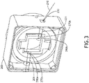
FIGS. 3 is a perspective drawing illustrating the mask including two prisms, in accordance with one or more embodiments of the present disclosure. -
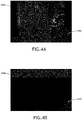
FIGS. 4A-4B are images showing artifacts on dark backgrounds, in accordance with one or more embodiments of the present disclosure. -
FIGS. 5A-5C are conceptual images illustrating an actual artifact, an ideal artifact, and a realistic artifact, in accordance with one or more embodiments of the present disclosure. -
FIGS. 6A-6C are tables showing the results of varying wavelength, voltage, and exposure time when producing an artifact, in accordance with one or more embodiments of the present disclosure. -
FIGS. 7A-7B are conceptual drawings illustrating the rotation of an artifact with respect to a calibration artifact, in accordance with one or more embodiments of the present disclosure. -
FIGS. 8A-8B are conceptual drawings illustrating the translation of an artifact with respect to a calibration artifact, in accordance with one or more embodiments of the present disclosure. -
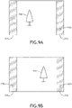
FIGS. 9A-9B are conceptual drawings illustrating the reflection of an artifact with respect to a calibration artifact, in accordance with one or more embodiments of the present disclosure. -
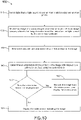
FIG. 10 is a flowchart illustrating a method of determining an orientation of an image, in accordance with one or more embodiments of the present disclosure. - Before explaining at least one embodiment of the inventive concepts disclosed herein in detail, it is to be understood that the inventive concepts are not limited in their application to the details of construction and the arrangement of the components or steps or methodologies set forth in the following description or illustrated in the drawings. In the following detailed description of embodiments of the present disclosure, numerous specific details are set forth in order to provide a more thorough understanding of the inventive concepts. However, it will be apparent to one of ordinary skill in the art having the benefit of the present disclosure that the inventive concepts disclosed herein may be practiced without these specific details. In other instances, well-known features may not be described in detail to avoid unnecessarily complicating the present disclosure. The inventive concepts disclosed herein are capable of other embodiments or of being practiced or carried out in various ways. Also, it is to be understood that the phraseology and terminology employed herein is for the purpose of description and should not be regarded as limiting.
- As used herein a letter following a reference numeral is intended to reference an embodiment of the feature or element that may be similar, but not necessarily identical, to a previously described element or feature bearing the same reference numeral (e.g., 1, 1a, 1b). Such shorthand notations are used for purposes of convenience only, and should not be construed to limit the inventive concepts disclosed herein in any way unless expressly stated to the contrary. Further, unless expressly stated to the contrary, "or" refers to an inclusive or and not to an exclusive or. For example, a condition A or B is satisfied by any one of the following: A is true (or present) and B is false (or not present), A is false (or not present) and B is true (or present), and both A and B are true (or present). In addition, use of the "a" or "an" are employed to describe elements and components of embodiments of the instant inventive concepts. This is done merely for convenience and to give a general sense of the inventive concepts, and "a" and "an" are intended to include one or at least one and the singular also includes the plural unless it is obvious that it is meant otherwise.
- Finally, as used herein any reference to "one embodiment" or "some embodiments" means that a particular element, feature, structure, or characteristic described in connection with the embodiment is included in at least one embodiment of the inventive concepts disclosed herein. The appearances of the phrase "in some embodiments" in various places in the specification are not necessarily all referring to the same embodiment, and embodiments of the inventive concepts disclosed may include one or more of the features expressly described or inherently present herein, or any combination or sub-combination of two or more such features, along with any other features which may not necessarily be expressly described or inherently present in the present disclosure.
- A conventional method of measuring the orientation (i.e., misalignment) of an image captured by an aircraft image sensor entails using intrinsic manufacturing flaws in the image sensor. Prior generations of image sensors are more prone to damage from cosmic rays due to relatively large pixels and less sophisticated manufacturing methods, which produce significant variability in pixel responsivities. In contrast, modern complementary metal oxide semiconductor (CMOS) technology is driving toward higher resolutions and more consistent manufacturing methods where the reliance on such intrinsic flaws or variability is not practical for measuring image orientation. Since it is not practical to use conventional orientation monitoring techniques that employ dead pixels or fixed pattern noise (FPN) in the image sensors, it may be desirable to employ techniques that do not rely on manufacturing flaws.
- Embodiments of the present disclosure are directed to an imaging system for an aircraft employing a light source, prisms, and pinholes to produce an artifact in the images collected by the imaging system. The artifact may then be used to determine the orientation of the collected images. If a detected misalignment exceeds a threshold misalignment, the image may be removed from the video stream shown to the user (e.g., pilot) of the aircraft. The imaging system may be, for example, part of an enhanced vision system (EVS) substantially similar to the EVS-3000 or EVS-3600 developed by Rockwell Collins, Inc. (Cedar Rapids, IA).
-
FIG. 1 is a diagram view of animaging system 100 for an aircraft, in accordance with one or more embodiments of the present disclosure. Theimaging system 100 may be in a cavity in thebody 110 of the aircraft and may include awindow 120, alens assembly 130, one ormore image sensors 150, ahousing 200, amask 201, and alight source 220. - The
window 120 may be transparent and may be adhered to thebody 110 such that the cavity is sealed from the outside environment. Thelens assembly 130 may include one or more lenses configured to direct light entering the cavity to the one ormore image sensors 150. The one ormore image sensors 150 may comprise a focal plane array (FPA) including an array of pixels (e.g., millions of pixels) and may be located at an image plane (i.e., field plane) of theimaging system 100 conjugate to an object plane in the surrounding environment. The one ormore image sensors 150 may comprise a CMOS photodiode array, although the present disclosure is not limited thereto. For example, in some embodiments, the one ormore image sensors 150 may comprise a charge-coupled device (CCD) photodiode array. The one ormore image sensors 150 may comprise one or more monochrome or RGB cameras configured to image optical wavelengths, and/or one or more infrared (IR) cameras configured to image short-wave IR (SWIR) and long-wave IR (LWIR) wavelengths. In some embodiments, the aircraft may includemultiple imaging systems 100 where eachimage sensor 150 is a different type of camera. For example, the aircraft may include anRGB sensor 150, anSWIR sensor 150, and anLWIR sensor 150. The images captured by each type ofsensor 150 may be fused or combined for an EVS output (i.e., a multi-spectral fusion video stream viewable to a pilot of the aircraft). - In some embodiments, a controller 160 (e.g., computer or computing system) including one or
more processors 163 and amemory 167 may be communicatively coupled to the one ormore image sensors 150. Program instructions may be stored on thememory 167, that, when executed by the one ormore processors 163, cause the one ormore processors 163 to perform functions, procedures, algorithms, methods, etc. described in the present disclosure. For example, in some embodiments, the program instructions may cause the one ormore processors 163 to receive an image of the surrounding environment of the aircraft from the one ormore image sensors 150. The centroid data and the extent data of an artifact may then be extracted from the image and compared to a calibration artifact (i.e., a reference artifact indicating a correct orientation) to determine the orientation of the captured image. - The one or
more processors 163 of thecontroller 160 may include any processor or processing element known in the art. For the purposes of the present disclosure, the term "processor" or "processing element" may be broadly defined to encompass any device having one or more processing or logic elements (e.g., one or more microprocessor devices, one or more application specific integrated circuit (ASIC) devices, one or more field programmable gate arrays (FPGAs), or one or more digital signal processors (DSPs). In this sense, the one ormore processors 163 may include any device configured to execute algorithms and/or instructions (e.g., program instructions stored in memory). In one embodiment, the one or more processors 132 may be embodied in an embedded system of an aircraft EVS. - The
memory medium 167 may include any storage medium known in the art suitable for storing program instructions executable by the associated one ormore processors 163. For example, thememory medium 167 may include a non-transitory memory medium. Byway of another example, thememory medium 167 may include, but is not limited to, a read-only memory (ROM), a random-access memory (RAM), a magnetic or optical memory device (e.g., disk), a magnetic tape, a solid-state drive and the like. It is further noted thatmemory medium 167 may be housed in a common controller housing with the one ormore processors 163. In one embodiment, thememory medium 167 may be located remotely with respect to the physical location of the one ormore processors 163 andcontroller 160. For instance, the one ormore processors 163 of thecontroller 160 may access a remote memory (e.g., server), accessible through a network (e.g., internet, intranet and the like). - The
light source 220 may be a light emitting diode (LED) or a laser diode configured to emit light 210 (e.g., a laser beam) in a wavelength range of from about 400 nm to about 2000 nm, although the present disclosure is not limited thereto. In some embodiments, the light 210 may have a wavelength within the response of the one ormore image sensors 150. As shown inFIG. 2 , the light 210 may be passed by an aperture orhole 230 in thehousing 200, and may then enter themask 201. In some embodiments, themask 201 comprises KOVAR™ (trademark of CRS Holdings, Inc., Delaware), FerNiCo I, FerNiCo II, or another nickel-cobalt ferrous alloy, although the present disclosure is not limited thereto. The thermal expansion coefficients of Ni-Co-Fe alloys may closely match the thermal expansion coefficients of glass, enabling glass seals such that the seal does not fracture with temperature changes. For this reason, themask 201 comprising the Ni-Co-Fe alloy may be adhered or affixed closely to a cover glass of theimage sensor 150 to minimize stray light. - As shown in
FIG. 3 , the light 210 may enter themask 201 through the aperture orhole 230 and thehousing 200. One ormore prisms 270a-b may direct the light 210 to one ormore pinholes 290a-b in themask 201. The light 210 may pass through one ormore pinholes 290a-b to create an artifact in images collected by theimage sensor 150. The one ormore prisms 270a-b may comprise plastic or glass and may be adhered or affixed to surfaces of themask 201 and/or thehousing 200. In some embodiments, the one ormore prisms 270a-b may reflect the light 210 by about 90° so that the light 210 is incident on the focal-plane array of the image sensor 150 (e.g., at a normal angle of incidence). - As shown in
FIGS. 4A-4B , theartifact 410 may appear as a white dot imposed on a dark background (e.g., shadowed regions on the sides of the collectedimages mask 201 may provide a high contrast area for theartifact 200. Theimage 400a was produced using a wavelength of 860 nm, an LED voltage of 1.20 V, and an exposure time of 20 milliseconds. Theimage 400b was produced using a wavelength of 860 nm, an LED voltage of 1.39 V, and an exposure time of 50 microseconds. Theartifact 410 may be asymmetrical, or, in some embodiments, may have one or more axes of symmetry. In some embodiments, theartifact 410 may be shaped by the one ormore pinholes 290a-b into a grating shape, a speckle pattern, a geometric shape, etc. In some embodiments, two ormore artifacts 410 may appear in the collected image (e.g., at opposite corners), where eachrespective artifact 410 is caused by the light 210 passing through arespective pinhole - It may be advantageous to employ the
artifact 410 imposed on a shadowed FPA region to determine the orientation of an image since thepresent imaging system 100 is versatile and robust compared to alternatives. For example, thepresent imaging system 100 may be employed in conditions of limited light such as instrument meteorological conditions (IMC) or night time. The present imaging system may also forego the requirement of an imaging processing algorithm to remove the artifact imposed on the image of the surroundings of the aircraft, for example, as described with respect toU.S. Pat. Appl. Serial. No. 17/176,931 entitled "CAMERA CORE MONITOR USING GRADIENT FILTER". -
FIGS. 5A-5C are conceptual images respectively illustrating anactual artifact 410 captured by animage sensor 150, anidealized artifact 510, and arealistic artifact 520, in accordance with one or more embodiments of the present disclosure. As shown, theidealized artifact 510 may have a circular shape with a digital number (DN; i.e., pixel intensity) greater than 0 inside the artifact and equal to zero outside the artifact. However, as illustrated by therealistic artifact 520, it may be reasonable to assume that the artifact is tilted and comprises concentric rings of varying intensity (as seen by the actual artifact 410). - The extent and centroid of the artifact may be estimated using DN threshold values. For example, to calculate the extent data, the artifact may be divided into four quadrants, and the edges of the artifact may be defined using a DN threshold (for example, the edges defining the intersection of pixels where DN = 0 and pixels where DN > 0). To calculate the centroid data, the arithmetic mean of the DN values of all of the pixels within the artifact edges may be calculated, and the centroid pixel may be defined at [x, y] coordinates (e.g., horizontal and vertical coordinates).
-
FIGS. 6A-6C are tables 610, 620 and 630 showing the results of experiments for a given wavelength of light within the sensor passband, while varying the voltage of the light source and/or and the exposure time, in accordance with one or more embodiments of the present disclosure. For each experiment, the DN threshold defining the edges of theartifact 410 was varied from 80 up to 250. The X-extent, Y-extent, X-centroid coordinate, and Y-centroid coordinate were calculated based on each DN threshold. - For the experiment represented by table 610, the wavelength of light was configured to be 840 nm, the voltage of the light source was configured to be 1.2 V, and the exposure time was configured to be 20 milliseconds. For the experiment represented by table 620, the wavelength of light was configured to be 840 nm, the voltage of the light source was configured to be 1.23 V, and the exposure time was configured to be 5 milliseconds. For the experiment represented by table 630, the wavelength of light was configured to be 840 nm, the voltage of the light source was configured to be 1.36 V, and the exposure time was configured to be 100 microseconds. As is shown, the centroid pixels are shifted by one or two pixels for some steps of DN threshold. This small shift indicates the relative stability of the estimated centroid, and provides insight into the range of pixel shift that may be used as a detection threshold to declare a misaligned image. Predictably, the extent decreases as the DN threshold increases.
-
FIGS. 7A-7B are conceptual drawings illustrating the rotation of theartifact 410 with respect to acalibration artifact 415, in accordance with one or more embodiments of the present disclosure. -
FIG. 7A illustrates an image of anobject 710, and acalibration artifact 415 imposed on a dark background 715 (e.g., masked areas 715). Theobject 710 appears with acorrect orientation 720, and thecalibration artifact 415 that appears in the image ofFIG. 7A may be used as a reference artifact. -
FIG. 7B illustrates an image of theobject 710 having anorientation 730 that is misaligned by rotation from thecorrect orientation 720. The extent data and the centroid data of theartifact 410 may be determined from the image ofFIG. 7B , and may be compared with thecalibration artifact 415 to determine the rotational misalignment (e.g., about 20°). Responsive to the rotational misalignment being greater than a threshold rotational misalignment within a selected tolerance (e.g., ±0.05°), the image ofFIG. 7B may be removed from the EVS video stream (e.g., removed from the stream presented on a display to a pilot of the aircraft). -
FIGS. 8A-8B are conceptual drawings illustrating the translation of theartifact 410 with respect to acalibration artifact 415, in accordance with one or more embodiments of the present disclosure. -
FIG. 8A illustrates an image of anobject 710, and acalibration artifact 415 imposed on a dark background 715 (e.g., masked areas 715). Theobject 710 appears with acorrect orientation 820, and thecalibration artifact 415 that appears in the image ofFIG. 8A may be used as a reference artifact. -
FIG. 8B illustrates an image of theobject 710 having anorientation 830 that is misaligned by translation from thecorrect orientation 820. The extent data and the centroid data of theartifact 410 may be determined from the image ofFIG. 8B , and may be compared with thecalibration artifact 415 to determine the translational misalignment. Responsive to the translational misalignment being greater than a threshold translational misalignment within a selected tolerance (e.g., ±10 pixels), the image ofFIG. 8B may be removed from the EVS video stream (e.g., removed from the stream presented on a display to a pilot of the aircraft). -
FIGS. 9A-9B are conceptual drawings illustrating the reflection of theartifact 410 with respect to acalibration artifact 415, in accordance with one or more embodiments of the present disclosure. -
FIG. 9A illustrates an image of anobject 710 and thecalibration artifact 415 imposed on a dark background 715 (e.g., masked areas 715). Theobject 710 appears with a correct orientation, and thecalibration artifact 415 that appears in the image ofFIG. 9A may be used as a reference artifact. -
FIG. 9B illustrates an image of theobject 710 having an orientation that is misaligned by reflection (mirror-symmetry) from the correct orientation. The extent data and the centroid data of theartifact 410 may be determined from the image ofFIG. 9B , and may be compared with thecalibration artifact 415 to determine the reflection misalignment. Responsive to a reflection misalignment being measured, the image ofFIG. 9B may be removed from the EVS video stream (e.g., removed from the stream presented on a display to a pilot of the aircraft). -
FIG. 10 is aflowchart 900 illustrating a method of determining the orientation of an image, in accordance with one or more embodiments of the present disclosure. - At
step 910, light may be directed from a light source to one or more pinholes within one or more masked regions using one or more prisms. - At
step 920, an image of the surrounding environment of the aircraft may be received (e.g., by the controller 160) from one or more image sensors (e.g., image sensors 150). The image may include artifact(s) within one or more masked regions based on the light passed by one or more pinholes. - At
step 930, the centroid data and the extent data of the artifact(s) may be determined. - At
step 940, the centroid data may be compared to calibration artifact(s) (i.e., the centroid of a reference artifact indicating a correct orientation) to determine the orientation of the artifact(s) and the captured image. The comparison may occur every n frames (for example, every three frames). - At
step 950, responsive to the centroid position of the artifact(s) indicating a misalignment (e.g., a rotational, translational, or reflection misalignment within a selected tolerance), the method may proceed to step 960, and responsive to the orientation of the artifact(s) indicating no misalignment (e.g., a correct alignment), the method may proceed to step 970. - At
step 960, responsive to a misalignment being detected in the image, the image may be removed from the video stream (e.g., EVS video stream) presented on a display to a user of the aircraft. Alternatively, atstep 970, responsive to no misalignment being detected in the image, the image may be left in the video stream. - It is believed that the present disclosure and many of its attendant advantages will be understood by the foregoing description, and it will be apparent that various changes may be made in the form, construction, and arrangement of the components without departing from the disclosed subject matter or without sacrificing all of its material advantages. The form described is merely explanatory, and it is the intention of the following claims to encompass and include such changes. Furthermore, it is to be understood that the invention is defined by the appended claims.
Claims (14)
- An imaging system for an aircraft, comprising:one or more image sensors (150) configured to image a surrounding environment of the aircraft;a light source (220) configured to emit light;a mask (201) including one or more prisms (270 a-b) configured to direct the light, and one or more pinholes (290 a-b) configured pass the light directed from the one or more prisms;a controller (160) communicatively coupled to the one or more image sensors, wherein the controller includes one or more processors (163) configured to execute program instructions causing the one or more processors to:receive an image of the surrounding environment of the aircraft from the one or more image sensors, wherein the image includes an artifact (410) based on the light passed by the one or more pinholes;determine extent data and centroid data of the artifact in the image; anddetermine an orientation of the artifact in the image with respect to a calibration artifact (415) using the centroid data.
- The imaging system of claim 1, wherein the artifact (410) appears on shadowed regions in the image to provide a high contrast between the artifact and the image.
- The imaging system of claim 1 or 2, wherein the artifact (410) is asymmetrical.
- The imaging system of claim 1 or 2, wherein the artifact is symmetrical.
- The imaging system of any preceding claim, wherein the light has a wavelength of from 400 nm to 850 nm.
- The imaging system of any preceding claim, wherein the image is captured by the one or more image sensors (150) with an exposure time of from 10 microseconds to 100 milliseconds.
- The imaging system of any preceding claim, wherein the light source is a light-emitting diode, LED.
- The imaging system of any of claims 1 to 6, wherein the light source is a laser diode.
- The imaging system of any preceding claim, wherein determining the orientation of the artifact (410) in the image with respect to the calibration artifact (415) comprises:
comparing an axis of symmetry of the artifact in the image with an axis of symmetry of the calibration artifact. - The imaging system of any preceding claim, wherein the orientation of the artifact indicates a rotation of the image with respect to the calibration artifact.
- The imaging system of any of claims 1 to 9, wherein the orientation of the artifact indicates a translation of the image with respect to the calibration artifact.
- The imaging system of any preceding claim, wherein the determined orientation of the image with respect to the calibration artifact indicates a reflection of the image with respect to the calibration artifact.
- The imaging system of any preceding claim, wherein the one or more image sensors comprise a complementary metal oxide semiconductor, CMOS, photodiode array.
- The imaging system of any preceding claim, wherein, responsive to the orientation of the artifact indicating a misalignment, the one or more processors are further configured to execute program instructions causing the one or more processors to:
remove the image from a video stream configured to be presented on a display to a user of the aircraft.
Applications Claiming Priority (1)
| Application Number | Priority Date | Filing Date | Title |
|---|---|---|---|
| US17/212,036 US11492140B2 (en) | 2021-03-25 | 2021-03-25 | Camera monitor using close proximity precision injection of light |
Publications (2)
| Publication Number | Publication Date |
|---|---|
| EP4064195A1 true EP4064195A1 (en) | 2022-09-28 |
| EP4064195B1 EP4064195B1 (en) | 2024-06-26 |
Family
ID=81344511
Family Applications (1)
| Application Number | Title | Priority Date | Filing Date |
|---|---|---|---|
| EP22164542.7A Active EP4064195B1 (en) | 2021-03-25 | 2022-03-25 | Camera monitor using close proximity precision injection of light |
Country Status (2)
| Country | Link |
|---|---|
| US (1) | US11492140B2 (en) |
| EP (1) | EP4064195B1 (en) |
Families Citing this family (1)
| Publication number | Priority date | Publication date | Assignee | Title |
|---|---|---|---|---|
| CN121032819B (en) * | 2025-10-29 | 2026-03-17 | 天津工业大学 | Multispectral image fusion method, system and equipment based on mask self-encoder |
Citations (3)
| Publication number | Priority date | Publication date | Assignee | Title |
|---|---|---|---|---|
| US7355179B1 (en) * | 2005-07-30 | 2008-04-08 | Rockwell Collins, Inc. | Scene imaging system integrity monitor and method thereof |
| US20170359573A1 (en) * | 2016-06-08 | 2017-12-14 | SAMSUNG SDS CO., LTD., Seoul, KOREA, REPUBLIC OF; | Method and apparatus for camera calibration using light source |
| US10606079B1 (en) * | 2017-06-06 | 2020-03-31 | Rockwell Collins, Inc. | Image integrity monitoring systems and methods for light processing based head up displays |
Family Cites Families (11)
| Publication number | Priority date | Publication date | Assignee | Title |
|---|---|---|---|---|
| GB2429864B (en) | 2005-09-01 | 2008-09-24 | Micron Technology Inc | Method and apparatus providing pixel array having automatic light control pixels and image capture pixels |
| KR101343105B1 (en) | 2007-12-18 | 2013-12-20 | 삼성디스플레이 주식회사 | Light sensor inspection unit, method of inspecting the same and display device |
| US8275213B2 (en) | 2008-05-08 | 2012-09-25 | Altasens, Inc. | Apparatus and method for gain correction |
| US8547456B1 (en) | 2009-09-30 | 2013-10-01 | Rockwell Collins, Inc. | System and method for monitoring inactive pixels in a scene imaging system |
| EP3047647B1 (en) | 2013-09-16 | 2020-05-27 | Prophesee | Dynamic, single photodiode pixel circuit and operating method thereof |
| DE102014215860A1 (en) | 2014-08-11 | 2016-02-11 | Robert Bosch Gmbh | Method and device for testing an image sensor and motor vehicle |
| EP3304166B1 (en) * | 2015-06-02 | 2019-06-26 | Life Technologies Corporation | Systems and methods for calibrating a structured illumination imaging system and for capturing a structured illumination image |
| US10319083B2 (en) * | 2016-07-15 | 2019-06-11 | Samsung Electronics Co., Ltd. | Image artifact detection and correction in scenes obtained from multiple visual images |
| US10109054B1 (en) | 2016-07-19 | 2018-10-23 | Rockwell Collins, Inc. | Monitoring COTS display devices for HWD/HUD/EVS via transparent photodetectors and imagers |
| CN111683212B (en) | 2020-07-20 | 2021-05-04 | 成都微光集电科技有限公司 | Image sensor and testing method thereof |
| US11508052B2 (en) * | 2020-09-10 | 2022-11-22 | Argo AI, LLC | Systems and methods for quantifying light flares in images |
-
2021
- 2021-03-25 US US17/212,036 patent/US11492140B2/en active Active
-
2022
- 2022-03-25 EP EP22164542.7A patent/EP4064195B1/en active Active
Patent Citations (3)
| Publication number | Priority date | Publication date | Assignee | Title |
|---|---|---|---|---|
| US7355179B1 (en) * | 2005-07-30 | 2008-04-08 | Rockwell Collins, Inc. | Scene imaging system integrity monitor and method thereof |
| US20170359573A1 (en) * | 2016-06-08 | 2017-12-14 | SAMSUNG SDS CO., LTD., Seoul, KOREA, REPUBLIC OF; | Method and apparatus for camera calibration using light source |
| US10606079B1 (en) * | 2017-06-06 | 2020-03-31 | Rockwell Collins, Inc. | Image integrity monitoring systems and methods for light processing based head up displays |
Also Published As
| Publication number | Publication date |
|---|---|
| US11492140B2 (en) | 2022-11-08 |
| EP4064195B1 (en) | 2024-06-26 |
| US20220306318A1 (en) | 2022-09-29 |
Similar Documents
| Publication | Publication Date | Title |
|---|---|---|
| US11265467B2 (en) | System and apparatus for co-registration and correlation between multi-modal imagery and method for same | |
| US10706514B2 (en) | Systems and methods for enhanced dynamic range infrared imaging | |
| US7924312B2 (en) | Infrared and visible-light image registration | |
| KR100777428B1 (en) | Image processing apparatus and method | |
| Wang et al. | Bionic orientation and visual enhancement with a novel polarization camera | |
| AU2015213322A1 (en) | Multiple pixel pitch for super resolution | |
| JP2024520598A (en) | Automatic calibration from epipolar distance in projected patterns | |
| EP4064195B1 (en) | Camera monitor using close proximity precision injection of light | |
| TW202146862A (en) | Infrared photography device | |
| CN207475756U (en) | The infrared stereo visual system of robot | |
| JP5493900B2 (en) | Imaging device | |
| US20190123075A1 (en) | Color pixel and range pixel combination unit | |
| Baker et al. | Advanced multifunctional detectors for laser-gated imaging applications | |
| EP4044119B1 (en) | CAMERA CORE MONITOR WITH GRADE FILTER | |
| CN109163809B (en) | Dual-band thermal imaging method and device with partially overlapping multi-aperture fields of view | |
| KR101398934B1 (en) | Wide field of view infrared camera with multi-combined image including the function of non-uniformity correction | |
| WO2026015170A1 (en) | Image compositing for adjacent cameras with low-parallax imaging | |
| WO2019036751A1 (en) | Enhanced video-based driver monitoring using phase detect sensors | |
| WO2021260598A1 (en) | Infrared wide-angle camera | |
| EP4071443B1 (en) | Camera agnostic core monitor incorporating projected images with high spatial frequency | |
| Efimov et al. | Digital multispectral images superimposition based on preliminary calibration or contour analysis: advantages and disadvantages | |
| US11290663B2 (en) | Thermal image sensing system and thermal image sensing method | |
| EP3884656B1 (en) | Device and method for observing a scene comprising a target | |
| KR20230117442A (en) | Imaging optical system with 3 mirrors | |
| Llull et al. | Lens array Stokes imaging polarimeter |
Legal Events
| Date | Code | Title | Description |
|---|---|---|---|
| PUAI | Public reference made under article 153(3) epc to a published international application that has entered the european phase |
Free format text: ORIGINAL CODE: 0009012 |
|
| STAA | Information on the status of an ep patent application or granted ep patent |
Free format text: STATUS: THE APPLICATION HAS BEEN PUBLISHED |
|
| AK | Designated contracting states |
Kind code of ref document: A1 Designated state(s): AL AT BE BG CH CY CZ DE DK EE ES FI FR GB GR HR HU IE IS IT LI LT LU LV MC MK MT NL NO PL PT RO RS SE SI SK SM TR |
|
| STAA | Information on the status of an ep patent application or granted ep patent |
Free format text: STATUS: REQUEST FOR EXAMINATION WAS MADE |
|
| 17P | Request for examination filed |
Effective date: 20230328 |
|
| RBV | Designated contracting states (corrected) |
Designated state(s): AL AT BE BG CH CY CZ DE DK EE ES FI FR GB GR HR HU IE IS IT LI LT LU LV MC MK MT NL NO PL PT RO RS SE SI SK SM TR |
|
| GRAP | Despatch of communication of intention to grant a patent |
Free format text: ORIGINAL CODE: EPIDOSNIGR1 |
|
| STAA | Information on the status of an ep patent application or granted ep patent |
Free format text: STATUS: GRANT OF PATENT IS INTENDED |
|
| RIC1 | Information provided on ipc code assigned before grant |
Ipc: H04N 17/00 20060101ALI20240110BHEP Ipc: G06T 7/00 20170101ALI20240110BHEP Ipc: B64D 47/08 20060101ALI20240110BHEP Ipc: G06V 10/24 20220101ALI20240110BHEP Ipc: G06T 7/73 20170101AFI20240110BHEP |
|
| INTG | Intention to grant announced |
Effective date: 20240212 |
|
| GRAS | Grant fee paid |
Free format text: ORIGINAL CODE: EPIDOSNIGR3 |
|
| GRAA | (expected) grant |
Free format text: ORIGINAL CODE: 0009210 |
|
| STAA | Information on the status of an ep patent application or granted ep patent |
Free format text: STATUS: THE PATENT HAS BEEN GRANTED |
|
| AK | Designated contracting states |
Kind code of ref document: B1 Designated state(s): AL AT BE BG CH CY CZ DE DK EE ES FI FR GB GR HR HU IE IS IT LI LT LU LV MC MK MT NL NO PL PT RO RS SE SI SK SM TR |
|
| REG | Reference to a national code |
Ref country code: GB Ref legal event code: FG4D |
|
| REG | Reference to a national code |
Ref country code: CH Ref legal event code: EP |
|
| REG | Reference to a national code |
Ref country code: DE Ref legal event code: R096 Ref document number: 602022004091 Country of ref document: DE |
|
| PG25 | Lapsed in a contracting state [announced via postgrant information from national office to epo] |
Ref country code: BG Free format text: LAPSE BECAUSE OF FAILURE TO SUBMIT A TRANSLATION OF THE DESCRIPTION OR TO PAY THE FEE WITHIN THE PRESCRIBED TIME-LIMIT Effective date: 20240626 |
|
| PG25 | Lapsed in a contracting state [announced via postgrant information from national office to epo] |
Ref country code: FI Free format text: LAPSE BECAUSE OF FAILURE TO SUBMIT A TRANSLATION OF THE DESCRIPTION OR TO PAY THE FEE WITHIN THE PRESCRIBED TIME-LIMIT Effective date: 20240626 Ref country code: HR Free format text: LAPSE BECAUSE OF FAILURE TO SUBMIT A TRANSLATION OF THE DESCRIPTION OR TO PAY THE FEE WITHIN THE PRESCRIBED TIME-LIMIT Effective date: 20240626 |
|
| REG | Reference to a national code |
Ref country code: LT Ref legal event code: MG9D |
|
| PG25 | Lapsed in a contracting state [announced via postgrant information from national office to epo] |
Ref country code: GR Free format text: LAPSE BECAUSE OF FAILURE TO SUBMIT A TRANSLATION OF THE DESCRIPTION OR TO PAY THE FEE WITHIN THE PRESCRIBED TIME-LIMIT Effective date: 20240927 |
|
| PG25 | Lapsed in a contracting state [announced via postgrant information from national office to epo] |
Ref country code: LV Free format text: LAPSE BECAUSE OF FAILURE TO SUBMIT A TRANSLATION OF THE DESCRIPTION OR TO PAY THE FEE WITHIN THE PRESCRIBED TIME-LIMIT Effective date: 20240626 |
|
| REG | Reference to a national code |
Ref country code: NL Ref legal event code: MP Effective date: 20240626 |
|
| PG25 | Lapsed in a contracting state [announced via postgrant information from national office to epo] |
Ref country code: NO Free format text: LAPSE BECAUSE OF FAILURE TO SUBMIT A TRANSLATION OF THE DESCRIPTION OR TO PAY THE FEE WITHIN THE PRESCRIBED TIME-LIMIT Effective date: 20240926 Ref country code: LV Free format text: LAPSE BECAUSE OF FAILURE TO SUBMIT A TRANSLATION OF THE DESCRIPTION OR TO PAY THE FEE WITHIN THE PRESCRIBED TIME-LIMIT Effective date: 20240626 Ref country code: HR Free format text: LAPSE BECAUSE OF FAILURE TO SUBMIT A TRANSLATION OF THE DESCRIPTION OR TO PAY THE FEE WITHIN THE PRESCRIBED TIME-LIMIT Effective date: 20240626 Ref country code: GR Free format text: LAPSE BECAUSE OF FAILURE TO SUBMIT A TRANSLATION OF THE DESCRIPTION OR TO PAY THE FEE WITHIN THE PRESCRIBED TIME-LIMIT Effective date: 20240927 Ref country code: FI Free format text: LAPSE BECAUSE OF FAILURE TO SUBMIT A TRANSLATION OF THE DESCRIPTION OR TO PAY THE FEE WITHIN THE PRESCRIBED TIME-LIMIT Effective date: 20240626 Ref country code: BG Free format text: LAPSE BECAUSE OF FAILURE TO SUBMIT A TRANSLATION OF THE DESCRIPTION OR TO PAY THE FEE WITHIN THE PRESCRIBED TIME-LIMIT Effective date: 20240626 Ref country code: RS Free format text: LAPSE BECAUSE OF FAILURE TO SUBMIT A TRANSLATION OF THE DESCRIPTION OR TO PAY THE FEE WITHIN THE PRESCRIBED TIME-LIMIT Effective date: 20240926 |
|
| PG25 | Lapsed in a contracting state [announced via postgrant information from national office to epo] |
Ref country code: NL Free format text: LAPSE BECAUSE OF FAILURE TO SUBMIT A TRANSLATION OF THE DESCRIPTION OR TO PAY THE FEE WITHIN THE PRESCRIBED TIME-LIMIT Effective date: 20240626 |
|
| REG | Reference to a national code |
Ref country code: AT Ref legal event code: MK05 Ref document number: 1698359 Country of ref document: AT Kind code of ref document: T Effective date: 20240626 |
|
| PG25 | Lapsed in a contracting state [announced via postgrant information from national office to epo] |
Ref country code: NL Free format text: LAPSE BECAUSE OF FAILURE TO SUBMIT A TRANSLATION OF THE DESCRIPTION OR TO PAY THE FEE WITHIN THE PRESCRIBED TIME-LIMIT Effective date: 20240626 |
|
| PG25 | Lapsed in a contracting state [announced via postgrant information from national office to epo] |
Ref country code: PT Free format text: LAPSE BECAUSE OF FAILURE TO SUBMIT A TRANSLATION OF THE DESCRIPTION OR TO PAY THE FEE WITHIN THE PRESCRIBED TIME-LIMIT Effective date: 20241028 |
|
| PG25 | Lapsed in a contracting state [announced via postgrant information from national office to epo] |
Ref country code: PT Free format text: LAPSE BECAUSE OF FAILURE TO SUBMIT A TRANSLATION OF THE DESCRIPTION OR TO PAY THE FEE WITHIN THE PRESCRIBED TIME-LIMIT Effective date: 20241028 |
|
| PG25 | Lapsed in a contracting state [announced via postgrant information from national office to epo] |
Ref country code: PL Free format text: LAPSE BECAUSE OF FAILURE TO SUBMIT A TRANSLATION OF THE DESCRIPTION OR TO PAY THE FEE WITHIN THE PRESCRIBED TIME-LIMIT Effective date: 20240626 |
|
| PG25 | Lapsed in a contracting state [announced via postgrant information from national office to epo] |
Ref country code: EE Free format text: LAPSE BECAUSE OF FAILURE TO SUBMIT A TRANSLATION OF THE DESCRIPTION OR TO PAY THE FEE WITHIN THE PRESCRIBED TIME-LIMIT Effective date: 20240626 |
|
| PG25 | Lapsed in a contracting state [announced via postgrant information from national office to epo] |
Ref country code: IS Free format text: LAPSE BECAUSE OF FAILURE TO SUBMIT A TRANSLATION OF THE DESCRIPTION OR TO PAY THE FEE WITHIN THE PRESCRIBED TIME-LIMIT Effective date: 20241026 Ref country code: AT Free format text: LAPSE BECAUSE OF FAILURE TO SUBMIT A TRANSLATION OF THE DESCRIPTION OR TO PAY THE FEE WITHIN THE PRESCRIBED TIME-LIMIT Effective date: 20240626 |
|
| PG25 | Lapsed in a contracting state [announced via postgrant information from national office to epo] |
Ref country code: CZ Free format text: LAPSE BECAUSE OF FAILURE TO SUBMIT A TRANSLATION OF THE DESCRIPTION OR TO PAY THE FEE WITHIN THE PRESCRIBED TIME-LIMIT Effective date: 20240626 |
|
| PG25 | Lapsed in a contracting state [announced via postgrant information from national office to epo] |
Ref country code: RO Free format text: LAPSE BECAUSE OF FAILURE TO SUBMIT A TRANSLATION OF THE DESCRIPTION OR TO PAY THE FEE WITHIN THE PRESCRIBED TIME-LIMIT Effective date: 20240626 Ref country code: SK Free format text: LAPSE BECAUSE OF FAILURE TO SUBMIT A TRANSLATION OF THE DESCRIPTION OR TO PAY THE FEE WITHIN THE PRESCRIBED TIME-LIMIT Effective date: 20240626 |
|
| PG25 | Lapsed in a contracting state [announced via postgrant information from national office to epo] |
Ref country code: ES Free format text: LAPSE BECAUSE OF FAILURE TO SUBMIT A TRANSLATION OF THE DESCRIPTION OR TO PAY THE FEE WITHIN THE PRESCRIBED TIME-LIMIT Effective date: 20240626 Ref country code: SM Free format text: LAPSE BECAUSE OF FAILURE TO SUBMIT A TRANSLATION OF THE DESCRIPTION OR TO PAY THE FEE WITHIN THE PRESCRIBED TIME-LIMIT Effective date: 20240626 |
|
| PG25 | Lapsed in a contracting state [announced via postgrant information from national office to epo] |
Ref country code: SM Free format text: LAPSE BECAUSE OF FAILURE TO SUBMIT A TRANSLATION OF THE DESCRIPTION OR TO PAY THE FEE WITHIN THE PRESCRIBED TIME-LIMIT Effective date: 20240626 Ref country code: SK Free format text: LAPSE BECAUSE OF FAILURE TO SUBMIT A TRANSLATION OF THE DESCRIPTION OR TO PAY THE FEE WITHIN THE PRESCRIBED TIME-LIMIT Effective date: 20240626 Ref country code: RO Free format text: LAPSE BECAUSE OF FAILURE TO SUBMIT A TRANSLATION OF THE DESCRIPTION OR TO PAY THE FEE WITHIN THE PRESCRIBED TIME-LIMIT Effective date: 20240626 Ref country code: PL Free format text: LAPSE BECAUSE OF FAILURE TO SUBMIT A TRANSLATION OF THE DESCRIPTION OR TO PAY THE FEE WITHIN THE PRESCRIBED TIME-LIMIT Effective date: 20240626 Ref country code: IS Free format text: LAPSE BECAUSE OF FAILURE TO SUBMIT A TRANSLATION OF THE DESCRIPTION OR TO PAY THE FEE WITHIN THE PRESCRIBED TIME-LIMIT Effective date: 20241026 Ref country code: ES Free format text: LAPSE BECAUSE OF FAILURE TO SUBMIT A TRANSLATION OF THE DESCRIPTION OR TO PAY THE FEE WITHIN THE PRESCRIBED TIME-LIMIT Effective date: 20240626 Ref country code: EE Free format text: LAPSE BECAUSE OF FAILURE TO SUBMIT A TRANSLATION OF THE DESCRIPTION OR TO PAY THE FEE WITHIN THE PRESCRIBED TIME-LIMIT Effective date: 20240626 Ref country code: CZ Free format text: LAPSE BECAUSE OF FAILURE TO SUBMIT A TRANSLATION OF THE DESCRIPTION OR TO PAY THE FEE WITHIN THE PRESCRIBED TIME-LIMIT Effective date: 20240626 Ref country code: AT Free format text: LAPSE BECAUSE OF FAILURE TO SUBMIT A TRANSLATION OF THE DESCRIPTION OR TO PAY THE FEE WITHIN THE PRESCRIBED TIME-LIMIT Effective date: 20240626 |
|
| PG25 | Lapsed in a contracting state [announced via postgrant information from national office to epo] |
Ref country code: IT Free format text: LAPSE BECAUSE OF FAILURE TO SUBMIT A TRANSLATION OF THE DESCRIPTION OR TO PAY THE FEE WITHIN THE PRESCRIBED TIME-LIMIT Effective date: 20240626 |
|
| REG | Reference to a national code |
Ref country code: DE Ref legal event code: R097 Ref document number: 602022004091 Country of ref document: DE |
|
| PG25 | Lapsed in a contracting state [announced via postgrant information from national office to epo] |
Ref country code: DK Free format text: LAPSE BECAUSE OF FAILURE TO SUBMIT A TRANSLATION OF THE DESCRIPTION OR TO PAY THE FEE WITHIN THE PRESCRIBED TIME-LIMIT Effective date: 20240626 |
|
| PLBE | No opposition filed within time limit |
Free format text: ORIGINAL CODE: 0009261 |
|
| STAA | Information on the status of an ep patent application or granted ep patent |
Free format text: STATUS: NO OPPOSITION FILED WITHIN TIME LIMIT |
|
| 26N | No opposition filed |
Effective date: 20250327 |
|
| PG25 | Lapsed in a contracting state [announced via postgrant information from national office to epo] |
Ref country code: SE Free format text: LAPSE BECAUSE OF FAILURE TO SUBMIT A TRANSLATION OF THE DESCRIPTION OR TO PAY THE FEE WITHIN THE PRESCRIBED TIME-LIMIT Effective date: 20240626 |
|
| PG25 | Lapsed in a contracting state [announced via postgrant information from national office to epo] |
Ref country code: MC Free format text: LAPSE BECAUSE OF FAILURE TO SUBMIT A TRANSLATION OF THE DESCRIPTION OR TO PAY THE FEE WITHIN THE PRESCRIBED TIME-LIMIT Effective date: 20240626 |
|
| REG | Reference to a national code |
Ref country code: CH Ref legal event code: H13 Free format text: ST27 STATUS EVENT CODE: U-0-0-H10-H13 (AS PROVIDED BY THE NATIONAL OFFICE) Effective date: 20251023 |
|
| PG25 | Lapsed in a contracting state [announced via postgrant information from national office to epo] |
Ref country code: LU Free format text: LAPSE BECAUSE OF NON-PAYMENT OF DUE FEES Effective date: 20250325 |
|
| REG | Reference to a national code |
Ref country code: BE Ref legal event code: MM Effective date: 20250331 |
|
| PG25 | Lapsed in a contracting state [announced via postgrant information from national office to epo] |
Ref country code: BE Free format text: LAPSE BECAUSE OF NON-PAYMENT OF DUE FEES Effective date: 20250331 |
|
| PG25 | Lapsed in a contracting state [announced via postgrant information from national office to epo] |
Ref country code: CH Free format text: LAPSE BECAUSE OF NON-PAYMENT OF DUE FEES Effective date: 20250331 |
|
| PG25 | Lapsed in a contracting state [announced via postgrant information from national office to epo] |
Ref country code: IE Free format text: LAPSE BECAUSE OF NON-PAYMENT OF DUE FEES Effective date: 20250325 |
|
| PGFP | Annual fee paid to national office [announced via postgrant information from national office to epo] |
Ref country code: GB Payment date: 20260220 Year of fee payment: 5 |
|
| PGFP | Annual fee paid to national office [announced via postgrant information from national office to epo] |
Ref country code: DE Payment date: 20260219 Year of fee payment: 5 |
|
| PGFP | Annual fee paid to national office [announced via postgrant information from national office to epo] |
Ref country code: FR Payment date: 20260219 Year of fee payment: 5 |