EP4063323A1 - Ferroelectric thin film, electronic element using same, and method for manufacturing ferroelectric thin film - Google Patents
Ferroelectric thin film, electronic element using same, and method for manufacturing ferroelectric thin film Download PDFInfo
- Publication number
- EP4063323A1 EP4063323A1 EP20904717.4A EP20904717A EP4063323A1 EP 4063323 A1 EP4063323 A1 EP 4063323A1 EP 20904717 A EP20904717 A EP 20904717A EP 4063323 A1 EP4063323 A1 EP 4063323A1
- Authority
- EP
- European Patent Office
- Prior art keywords
- thin film
- ferroelectric thin
- ferroelectric
- range
- less
- Prior art date
- Legal status (The legal status is an assumption and is not a legal conclusion. Google has not performed a legal analysis and makes no representation as to the accuracy of the status listed.)
- Pending
Links
Images









Classifications
-
- C—CHEMISTRY; METALLURGY
- C01—INORGANIC CHEMISTRY
- C01B—NON-METALLIC ELEMENTS; COMPOUNDS THEREOF; METALLOIDS OR COMPOUNDS THEREOF NOT COVERED BY SUBCLASS C01C
- C01B21/00—Nitrogen; Compounds thereof
- C01B21/06—Binary compounds of nitrogen with metals, with silicon, or with boron, or with carbon, i.e. nitrides; Compounds of nitrogen with more than one metal, silicon or boron
-
- C—CHEMISTRY; METALLURGY
- C30—CRYSTAL GROWTH
- C30B—SINGLE-CRYSTAL GROWTH; UNIDIRECTIONAL SOLIDIFICATION OF EUTECTIC MATERIAL OR UNIDIRECTIONAL DEMIXING OF EUTECTOID MATERIAL; REFINING BY ZONE-MELTING OF MATERIAL; PRODUCTION OF A HOMOGENEOUS POLYCRYSTALLINE MATERIAL WITH DEFINED STRUCTURE; SINGLE CRYSTALS OR HOMOGENEOUS POLYCRYSTALLINE MATERIAL WITH DEFINED STRUCTURE; AFTER-TREATMENT OF SINGLE CRYSTALS OR A HOMOGENEOUS POLYCRYSTALLINE MATERIAL WITH DEFINED STRUCTURE; APPARATUS THEREFOR
- C30B29/00—Single crystals or homogeneous polycrystalline material with defined structure characterised by the material or by their shape
- C30B29/10—Inorganic compounds or compositions
- C30B29/38—Nitrides
-
- G—PHYSICS
- G11—INFORMATION STORAGE
- G11C—STATIC STORES
- G11C11/00—Digital stores characterised by the use of particular electric or magnetic storage elements; Storage elements therefor
- G11C11/21—Digital stores characterised by the use of particular electric or magnetic storage elements; Storage elements therefor using electric elements
- G11C11/22—Digital stores characterised by the use of particular electric or magnetic storage elements; Storage elements therefor using electric elements using ferroelectric elements
- G11C11/223—Digital stores characterised by the use of particular electric or magnetic storage elements; Storage elements therefor using electric elements using ferroelectric elements using MOS with ferroelectric gate insulating film
-
- C—CHEMISTRY; METALLURGY
- C01—INORGANIC CHEMISTRY
- C01B—NON-METALLIC ELEMENTS; COMPOUNDS THEREOF; METALLOIDS OR COMPOUNDS THEREOF NOT COVERED BY SUBCLASS C01C
- C01B21/00—Nitrogen; Compounds thereof
- C01B21/06—Binary compounds of nitrogen with metals, with silicon, or with boron, or with carbon, i.e. nitrides; Compounds of nitrogen with more than one metal, silicon or boron
- C01B21/0602—Binary compounds of nitrogen with metals, with silicon, or with boron, or with carbon, i.e. nitrides; Compounds of nitrogen with more than one metal, silicon or boron with two or more other elements chosen from metals, silicon or boron
-
- C—CHEMISTRY; METALLURGY
- C01—INORGANIC CHEMISTRY
- C01F—COMPOUNDS OF THE METALS BERYLLIUM, MAGNESIUM, ALUMINIUM, CALCIUM, STRONTIUM, BARIUM, RADIUM, THORIUM, OR OF THE RARE-EARTH METALS
- C01F17/00—Compounds of rare earth metals
- C01F17/10—Preparation or treatment, e.g. separation or purification
-
- C—CHEMISTRY; METALLURGY
- C01—INORGANIC CHEMISTRY
- C01F—COMPOUNDS OF THE METALS BERYLLIUM, MAGNESIUM, ALUMINIUM, CALCIUM, STRONTIUM, BARIUM, RADIUM, THORIUM, OR OF THE RARE-EARTH METALS
- C01F17/00—Compounds of rare earth metals
- C01F17/30—Compounds containing rare earth metals and at least one element other than a rare earth metal, oxygen or hydrogen, e.g. La4S3Br6
-
- C—CHEMISTRY; METALLURGY
- C01—INORGANIC CHEMISTRY
- C01G—COMPOUNDS CONTAINING METALS NOT COVERED BY SUBCLASSES C01D OR C01F
- C01G15/00—Compounds of gallium, indium or thallium
-
- C—CHEMISTRY; METALLURGY
- C01—INORGANIC CHEMISTRY
- C01G—COMPOUNDS CONTAINING METALS NOT COVERED BY SUBCLASSES C01D OR C01F
- C01G33/00—Compounds of niobium
-
- C—CHEMISTRY; METALLURGY
- C04—CEMENTS; CONCRETE; ARTIFICIAL STONE; CERAMICS; REFRACTORIES
- C04B—LIME, MAGNESIA; SLAG; CEMENTS; COMPOSITIONS THEREOF, e.g. MORTARS, CONCRETE OR LIKE BUILDING MATERIALS; ARTIFICIAL STONE; CERAMICS; REFRACTORIES; TREATMENT OF NATURAL STONE
- C04B35/00—Shaped ceramic products characterised by their composition; Ceramics compositions; Processing powders of inorganic compounds preparatory to the manufacturing of ceramic products
- C04B35/515—Shaped ceramic products characterised by their composition; Ceramics compositions; Processing powders of inorganic compounds preparatory to the manufacturing of ceramic products based on non-oxide ceramics
- C04B35/58—Shaped ceramic products characterised by their composition; Ceramics compositions; Processing powders of inorganic compounds preparatory to the manufacturing of ceramic products based on non-oxide ceramics based on borides, nitrides, i.e. nitrides, oxynitrides, carbonitrides or oxycarbonitrides or silicides
-
- C—CHEMISTRY; METALLURGY
- C04—CEMENTS; CONCRETE; ARTIFICIAL STONE; CERAMICS; REFRACTORIES
- C04B—LIME, MAGNESIA; SLAG; CEMENTS; COMPOSITIONS THEREOF, e.g. MORTARS, CONCRETE OR LIKE BUILDING MATERIALS; ARTIFICIAL STONE; CERAMICS; REFRACTORIES; TREATMENT OF NATURAL STONE
- C04B35/00—Shaped ceramic products characterised by their composition; Ceramics compositions; Processing powders of inorganic compounds preparatory to the manufacturing of ceramic products
- C04B35/515—Shaped ceramic products characterised by their composition; Ceramics compositions; Processing powders of inorganic compounds preparatory to the manufacturing of ceramic products based on non-oxide ceramics
- C04B35/58—Shaped ceramic products characterised by their composition; Ceramics compositions; Processing powders of inorganic compounds preparatory to the manufacturing of ceramic products based on non-oxide ceramics based on borides, nitrides, i.e. nitrides, oxynitrides, carbonitrides or oxycarbonitrides or silicides
- C04B35/581—Shaped ceramic products characterised by their composition; Ceramics compositions; Processing powders of inorganic compounds preparatory to the manufacturing of ceramic products based on non-oxide ceramics based on borides, nitrides, i.e. nitrides, oxynitrides, carbonitrides or oxycarbonitrides or silicides based on aluminium nitride
-
- C—CHEMISTRY; METALLURGY
- C23—COATING METALLIC MATERIAL; COATING MATERIAL WITH METALLIC MATERIAL; CHEMICAL SURFACE TREATMENT; DIFFUSION TREATMENT OF METALLIC MATERIAL; COATING BY VACUUM EVAPORATION, BY SPUTTERING, BY ION IMPLANTATION OR BY CHEMICAL VAPOUR DEPOSITION, IN GENERAL; INHIBITING CORROSION OF METALLIC MATERIAL OR INCRUSTATION IN GENERAL
- C23C—COATING METALLIC MATERIAL; COATING MATERIAL WITH METALLIC MATERIAL; SURFACE TREATMENT OF METALLIC MATERIAL BY DIFFUSION INTO THE SURFACE, BY CHEMICAL CONVERSION OR SUBSTITUTION; COATING BY VACUUM EVAPORATION, BY SPUTTERING, BY ION IMPLANTATION OR BY CHEMICAL VAPOUR DEPOSITION, IN GENERAL
- C23C14/00—Coating by vacuum evaporation, by sputtering or by ion implantation of the coating forming material
- C23C14/0021—Reactive sputtering or evaporation
- C23C14/0036—Reactive sputtering
-
- C—CHEMISTRY; METALLURGY
- C23—COATING METALLIC MATERIAL; COATING MATERIAL WITH METALLIC MATERIAL; CHEMICAL SURFACE TREATMENT; DIFFUSION TREATMENT OF METALLIC MATERIAL; COATING BY VACUUM EVAPORATION, BY SPUTTERING, BY ION IMPLANTATION OR BY CHEMICAL VAPOUR DEPOSITION, IN GENERAL; INHIBITING CORROSION OF METALLIC MATERIAL OR INCRUSTATION IN GENERAL
- C23C—COATING METALLIC MATERIAL; COATING MATERIAL WITH METALLIC MATERIAL; SURFACE TREATMENT OF METALLIC MATERIAL BY DIFFUSION INTO THE SURFACE, BY CHEMICAL CONVERSION OR SUBSTITUTION; COATING BY VACUUM EVAPORATION, BY SPUTTERING, BY ION IMPLANTATION OR BY CHEMICAL VAPOUR DEPOSITION, IN GENERAL
- C23C14/00—Coating by vacuum evaporation, by sputtering or by ion implantation of the coating forming material
- C23C14/06—Coating by vacuum evaporation, by sputtering or by ion implantation of the coating forming material characterised by the coating material
-
- C—CHEMISTRY; METALLURGY
- C23—COATING METALLIC MATERIAL; COATING MATERIAL WITH METALLIC MATERIAL; CHEMICAL SURFACE TREATMENT; DIFFUSION TREATMENT OF METALLIC MATERIAL; COATING BY VACUUM EVAPORATION, BY SPUTTERING, BY ION IMPLANTATION OR BY CHEMICAL VAPOUR DEPOSITION, IN GENERAL; INHIBITING CORROSION OF METALLIC MATERIAL OR INCRUSTATION IN GENERAL
- C23C—COATING METALLIC MATERIAL; COATING MATERIAL WITH METALLIC MATERIAL; SURFACE TREATMENT OF METALLIC MATERIAL BY DIFFUSION INTO THE SURFACE, BY CHEMICAL CONVERSION OR SUBSTITUTION; COATING BY VACUUM EVAPORATION, BY SPUTTERING, BY ION IMPLANTATION OR BY CHEMICAL VAPOUR DEPOSITION, IN GENERAL
- C23C14/00—Coating by vacuum evaporation, by sputtering or by ion implantation of the coating forming material
- C23C14/06—Coating by vacuum evaporation, by sputtering or by ion implantation of the coating forming material characterised by the coating material
- C23C14/0641—Nitrides
-
- C—CHEMISTRY; METALLURGY
- C23—COATING METALLIC MATERIAL; COATING MATERIAL WITH METALLIC MATERIAL; CHEMICAL SURFACE TREATMENT; DIFFUSION TREATMENT OF METALLIC MATERIAL; COATING BY VACUUM EVAPORATION, BY SPUTTERING, BY ION IMPLANTATION OR BY CHEMICAL VAPOUR DEPOSITION, IN GENERAL; INHIBITING CORROSION OF METALLIC MATERIAL OR INCRUSTATION IN GENERAL
- C23C—COATING METALLIC MATERIAL; COATING MATERIAL WITH METALLIC MATERIAL; SURFACE TREATMENT OF METALLIC MATERIAL BY DIFFUSION INTO THE SURFACE, BY CHEMICAL CONVERSION OR SUBSTITUTION; COATING BY VACUUM EVAPORATION, BY SPUTTERING, BY ION IMPLANTATION OR BY CHEMICAL VAPOUR DEPOSITION, IN GENERAL
- C23C14/00—Coating by vacuum evaporation, by sputtering or by ion implantation of the coating forming material
- C23C14/22—Coating by vacuum evaporation, by sputtering or by ion implantation of the coating forming material characterised by the process of coating
- C23C14/34—Sputtering
-
- C—CHEMISTRY; METALLURGY
- C23—COATING METALLIC MATERIAL; COATING MATERIAL WITH METALLIC MATERIAL; CHEMICAL SURFACE TREATMENT; DIFFUSION TREATMENT OF METALLIC MATERIAL; COATING BY VACUUM EVAPORATION, BY SPUTTERING, BY ION IMPLANTATION OR BY CHEMICAL VAPOUR DEPOSITION, IN GENERAL; INHIBITING CORROSION OF METALLIC MATERIAL OR INCRUSTATION IN GENERAL
- C23C—COATING METALLIC MATERIAL; COATING MATERIAL WITH METALLIC MATERIAL; SURFACE TREATMENT OF METALLIC MATERIAL BY DIFFUSION INTO THE SURFACE, BY CHEMICAL CONVERSION OR SUBSTITUTION; COATING BY VACUUM EVAPORATION, BY SPUTTERING, BY ION IMPLANTATION OR BY CHEMICAL VAPOUR DEPOSITION, IN GENERAL
- C23C14/00—Coating by vacuum evaporation, by sputtering or by ion implantation of the coating forming material
- C23C14/22—Coating by vacuum evaporation, by sputtering or by ion implantation of the coating forming material characterised by the process of coating
- C23C14/34—Sputtering
- C23C14/3464—Sputtering using more than one target
-
- C—CHEMISTRY; METALLURGY
- C30—CRYSTAL GROWTH
- C30B—SINGLE-CRYSTAL GROWTH; UNIDIRECTIONAL SOLIDIFICATION OF EUTECTIC MATERIAL OR UNIDIRECTIONAL DEMIXING OF EUTECTOID MATERIAL; REFINING BY ZONE-MELTING OF MATERIAL; PRODUCTION OF A HOMOGENEOUS POLYCRYSTALLINE MATERIAL WITH DEFINED STRUCTURE; SINGLE CRYSTALS OR HOMOGENEOUS POLYCRYSTALLINE MATERIAL WITH DEFINED STRUCTURE; AFTER-TREATMENT OF SINGLE CRYSTALS OR A HOMOGENEOUS POLYCRYSTALLINE MATERIAL WITH DEFINED STRUCTURE; APPARATUS THEREFOR
- C30B23/00—Single-crystal growth by condensing evaporated or sublimed materials
- C30B23/02—Epitaxial-layer growth
- C30B23/08—Epitaxial-layer growth by condensing ionised vapours
-
- C—CHEMISTRY; METALLURGY
- C30—CRYSTAL GROWTH
- C30B—SINGLE-CRYSTAL GROWTH; UNIDIRECTIONAL SOLIDIFICATION OF EUTECTIC MATERIAL OR UNIDIRECTIONAL DEMIXING OF EUTECTOID MATERIAL; REFINING BY ZONE-MELTING OF MATERIAL; PRODUCTION OF A HOMOGENEOUS POLYCRYSTALLINE MATERIAL WITH DEFINED STRUCTURE; SINGLE CRYSTALS OR HOMOGENEOUS POLYCRYSTALLINE MATERIAL WITH DEFINED STRUCTURE; AFTER-TREATMENT OF SINGLE CRYSTALS OR A HOMOGENEOUS POLYCRYSTALLINE MATERIAL WITH DEFINED STRUCTURE; APPARATUS THEREFOR
- C30B29/00—Single crystals or homogeneous polycrystalline material with defined structure characterised by the material or by their shape
- C30B29/10—Inorganic compounds or compositions
- C30B29/40—AIIIBV compounds wherein A is B, Al, Ga, In or Tl and B is N, P, As, Sb or Bi
- C30B29/403—AIII-nitrides
- C30B29/406—Gallium nitride
-
- H—ELECTRICITY
- H10—SEMICONDUCTOR DEVICES; ELECTRIC SOLID-STATE DEVICES NOT OTHERWISE PROVIDED FOR
- H10B—ELECTRONIC MEMORY DEVICES
- H10B51/00—Ferroelectric RAM [FeRAM] devices comprising ferroelectric memory transistors
-
- H—ELECTRICITY
- H10—SEMICONDUCTOR DEVICES; ELECTRIC SOLID-STATE DEVICES NOT OTHERWISE PROVIDED FOR
- H10B—ELECTRONIC MEMORY DEVICES
- H10B53/00—Ferroelectric RAM [FeRAM] devices comprising ferroelectric memory capacitors
-
- H—ELECTRICITY
- H10—SEMICONDUCTOR DEVICES; ELECTRIC SOLID-STATE DEVICES NOT OTHERWISE PROVIDED FOR
- H10D—INORGANIC ELECTRIC SEMICONDUCTOR DEVICES
- H10D64/00—Electrodes of devices having potential barriers
- H10D64/01—Manufacture or treatment
- H10D64/031—Manufacture or treatment of data-storage electrodes
- H10D64/033—Manufacture or treatment of data-storage electrodes comprising ferroelectric layers
-
- H—ELECTRICITY
- H10—SEMICONDUCTOR DEVICES; ELECTRIC SOLID-STATE DEVICES NOT OTHERWISE PROVIDED FOR
- H10D—INORGANIC ELECTRIC SEMICONDUCTOR DEVICES
- H10D64/00—Electrodes of devices having potential barriers
- H10D64/60—Electrodes characterised by their materials
- H10D64/66—Electrodes having a conductor capacitively coupled to a semiconductor by an insulator, e.g. MIS electrodes
- H10D64/68—Electrodes having a conductor capacitively coupled to a semiconductor by an insulator, e.g. MIS electrodes characterised by the insulator, e.g. by the gate insulator
- H10D64/689—Electrodes having a conductor capacitively coupled to a semiconductor by an insulator, e.g. MIS electrodes characterised by the insulator, e.g. by the gate insulator having ferroelectric layers
-
- H—ELECTRICITY
- H10—SEMICONDUCTOR DEVICES; ELECTRIC SOLID-STATE DEVICES NOT OTHERWISE PROVIDED FOR
- H10N—ELECTRIC SOLID-STATE DEVICES NOT OTHERWISE PROVIDED FOR
- H10N30/00—Piezoelectric or electrostrictive devices
- H10N30/01—Manufacture or treatment
- H10N30/07—Forming of piezoelectric or electrostrictive parts or bodies on an electrical element or another base
- H10N30/074—Forming of piezoelectric or electrostrictive parts or bodies on an electrical element or another base by depositing piezoelectric or electrostrictive layers, e.g. aerosol or screen printing
- H10N30/076—Forming of piezoelectric or electrostrictive parts or bodies on an electrical element or another base by depositing piezoelectric or electrostrictive layers, e.g. aerosol or screen printing by vapour phase deposition
-
- H—ELECTRICITY
- H10—SEMICONDUCTOR DEVICES; ELECTRIC SOLID-STATE DEVICES NOT OTHERWISE PROVIDED FOR
- H10N—ELECTRIC SOLID-STATE DEVICES NOT OTHERWISE PROVIDED FOR
- H10N30/00—Piezoelectric or electrostrictive devices
- H10N30/80—Constructional details
-
- H—ELECTRICITY
- H10—SEMICONDUCTOR DEVICES; ELECTRIC SOLID-STATE DEVICES NOT OTHERWISE PROVIDED FOR
- H10N—ELECTRIC SOLID-STATE DEVICES NOT OTHERWISE PROVIDED FOR
- H10N30/00—Piezoelectric or electrostrictive devices
- H10N30/80—Constructional details
- H10N30/85—Piezoelectric or electrostrictive active materials
- H10N30/853—Ceramic compositions
-
- H—ELECTRICITY
- H10—SEMICONDUCTOR DEVICES; ELECTRIC SOLID-STATE DEVICES NOT OTHERWISE PROVIDED FOR
- H10P—GENERIC PROCESSES OR APPARATUS FOR THE MANUFACTURE OR TREATMENT OF DEVICES COVERED BY CLASS H10
- H10P14/00—Formation of materials, e.g. in the shape of layers or pillars
- H10P14/60—Formation of materials, e.g. in the shape of layers or pillars of insulating materials
- H10P14/63—Formation of materials, e.g. in the shape of layers or pillars of insulating materials characterised by the formation processes
- H10P14/6326—Deposition processes
- H10P14/6328—Deposition from the gas or vapour phase
- H10P14/6334—Deposition from the gas or vapour phase using decomposition or reaction of gaseous or vapour phase compounds, i.e. chemical vapour deposition
- H10P14/6339—Deposition from the gas or vapour phase using decomposition or reaction of gaseous or vapour phase compounds, i.e. chemical vapour deposition deposition by cyclic CVD, e.g. ALD, ALE or pulsed CVD
-
- C—CHEMISTRY; METALLURGY
- C04—CEMENTS; CONCRETE; ARTIFICIAL STONE; CERAMICS; REFRACTORIES
- C04B—LIME, MAGNESIA; SLAG; CEMENTS; COMPOSITIONS THEREOF, e.g. MORTARS, CONCRETE OR LIKE BUILDING MATERIALS; ARTIFICIAL STONE; CERAMICS; REFRACTORIES; TREATMENT OF NATURAL STONE
- C04B2235/00—Aspects relating to ceramic starting mixtures or sintered ceramic products
- C04B2235/02—Composition of constituents of the starting material or of secondary phases of the final product
- C04B2235/30—Constituents and secondary phases not being of a fibrous nature
- C04B2235/38—Non-oxide ceramic constituents or additives
- C04B2235/3852—Nitrides, e.g. oxynitrides, carbonitrides, oxycarbonitrides, lithium nitride, magnesium nitride
-
- C—CHEMISTRY; METALLURGY
- C04—CEMENTS; CONCRETE; ARTIFICIAL STONE; CERAMICS; REFRACTORIES
- C04B—LIME, MAGNESIA; SLAG; CEMENTS; COMPOSITIONS THEREOF, e.g. MORTARS, CONCRETE OR LIKE BUILDING MATERIALS; ARTIFICIAL STONE; CERAMICS; REFRACTORIES; TREATMENT OF NATURAL STONE
- C04B2235/00—Aspects relating to ceramic starting mixtures or sintered ceramic products
- C04B2235/02—Composition of constituents of the starting material or of secondary phases of the final product
- C04B2235/30—Constituents and secondary phases not being of a fibrous nature
- C04B2235/38—Non-oxide ceramic constituents or additives
- C04B2235/3852—Nitrides, e.g. oxynitrides, carbonitrides, oxycarbonitrides, lithium nitride, magnesium nitride
- C04B2235/3865—Aluminium nitrides
-
- C—CHEMISTRY; METALLURGY
- C04—CEMENTS; CONCRETE; ARTIFICIAL STONE; CERAMICS; REFRACTORIES
- C04B—LIME, MAGNESIA; SLAG; CEMENTS; COMPOSITIONS THEREOF, e.g. MORTARS, CONCRETE OR LIKE BUILDING MATERIALS; ARTIFICIAL STONE; CERAMICS; REFRACTORIES; TREATMENT OF NATURAL STONE
- C04B2235/00—Aspects relating to ceramic starting mixtures or sintered ceramic products
- C04B2235/02—Composition of constituents of the starting material or of secondary phases of the final product
- C04B2235/30—Constituents and secondary phases not being of a fibrous nature
- C04B2235/38—Non-oxide ceramic constituents or additives
- C04B2235/3852—Nitrides, e.g. oxynitrides, carbonitrides, oxycarbonitrides, lithium nitride, magnesium nitride
- C04B2235/3886—Refractory metal nitrides, e.g. vanadium nitride, tungsten nitride
Definitions
- the present invention relates to a ferroelectric thin film, an electronic device using the same, and a method for producing the ferroelectric thin film.
- Ferroelectric bodies (ferroelectric thin films), a kind of dielectric body, refer to a substance in which electric dipoles are aligned in the absence of an external electric field and directions of the dipoles can vary depending on the electric field.
- Such ferroelectric bodies are a dielectric body having pyroelectric properties and piezoelectric properties in addition to ferroelectric properties.
- the ferroelectric bodies are used as a ferroelectric random access memory (FeRAM) or the like that uses ferroelectric properties, or as an actuator or the like that uses the piezoelectric effect.
- FeRAM ferroelectric random access memory
- Non-Patent Literature 1 scandium-doped aluminum nitride having excellent ferroelectric properties has been recently reported (see Non-Patent Literature 1).
- Non-Patent Literature 1 Simon Fichtner, Niklas Wolff, Fabian Lofink, Lorenz Kienle, and Bernhard Wagner, J. Appl. Phys. 125, 114103(2019 )
- Non-Patent Literature 1 describes that when the concentration X of scandium (Sc) in Sc-doped aluminum nitride (Al 1-x Sc x N) is lower than 0.22, dielectric breakdown occurs before an electric field reaches a coercive electric field.
- a ferroelectric thin film including Al 1-x Sc x N has a problem in which when a sufficient thickness (for example, 600 nm or more) of the ferroelectric thin film is not available, the ferroelectric thin film exhibits insufficient ferroelectric properties and lacks stability when applied to practical use.
- the inventors of the present invention have intensively performed research and development on the aforementioned problems, and as a result found a ferroelectric thin film that is innovative as described below, an electronic device using the same, and a method for producing the ferroelectric thin film.
- a first aspect of the present invention to solve the problems is a ferroelectric thin film represented by a chemical formula M1 1-X M2 X N, wherein M1 is at least one element selected from aluminum (Al) and gallium (Ga), M2 is at least one element selected from magnesium (Mg), scandium (Sc), ytterbium (Yb), and niobium (Nb), and X is within the range of 0 or more and 1 or less.
- the ferroelectric thin film that has high ferroelectric properties and high stability can be provided.
- a second aspect of the present invention is the ferroelectric thin film according to the first aspect, wherein M1 is Al, M2 is Sc, and X is within the range of more than 0 and 0.219 or less.
- the ferroelectric thin film that has much higher ferroelectric properties and higher stability than the ferroelectric thin film including Al 1-x Sc x N disclosed in Non-Patent Literature 1 although the Sc concentration is lower than the Sc concentration at which it is recognized that the thin film cannot be formed.
- a third aspect of the present invention is the ferroelectric thin film according to the first aspect, wherein M1 is Al, M2 is Sc, and X is within the range of 0.065 or more and 0.219 or less.
- the ferroelectric thin film that has much higher ferroelectric properties and higher stability than the ferroelectric thin film including Al 1- xScxN disclosed in Non-Patent Literature 1 although the Sc concentration is lower than the Sc concentration at which it is recognized that the thin film cannot be formed.
- a fourth aspect of the present invention is the ferroelectric thin film according to the first aspect, wherein M1 is Al, M2 is Sc, and X is within the range of 0.16 or more and 0.219 or less.
- the ferroelectric thin film that has much higher ferroelectric properties and higher stability than the ferroelectric thin film including Al 1- xScxN disclosed in Non-Patent Literature 1 although the Sc concentration is lower than the Sc concentration at which it is recognized that the thin film cannot be formed.
- a fifth aspect of the present invention is the ferroelectric thin film according to the first aspect, wherein M1 is Al, M2 is Mg 1-Y Nb Y , X is within the range of 0 or more and 1 or less, and Y is within the range of 0 or more and 1 or less.
- the ferroelectric thin film that is more inexpensive and have higher ferroelectric properties and higher stability can be provided.
- a sixth aspect of the present invention is the ferroelectric thin film according to the first aspect, wherein M1 is Ga, M2 is Sc, and X is within the range of 0 or more and 1 or less.
- the ferroelectric thin film that has higher ferroelectric properties and higher stability can be provided.
- This aspect is highly applicable to current gallium nitride semiconductors and their production processes, and a production process of this aspect can easily be incorporated into the production processes for the current gallium nitride semiconductors.
- a seventh aspect of the present invention is the ferroelectric thin film according to the first aspect, wherein M1 is Al, M2 is Yb, and X is within the range of 0 or more and 1 or less.
- the ferroelectric thin film that has higher ferroelectric properties and higher stability can be provided.
- An eighth aspect of the present invention is the ferroelectric thin film according to the first aspect, wherein M1 is Ga, and X is 0.
- the ferroelectric thin film that has higher ferroelectric properties and higher stability can be provided.
- This aspect is highly applicable to the current gallium nitride semiconductors and their production processes, and a production process of this aspect can easily be incorporated into the production processes for the current gallium nitride semiconductors.
- a ninth aspect of the present invention is the ferroelectric thin film according to any one of the first to eighth aspects, wherein u calculated by the following expression is within the range of 0.375 or more and less than 0.5.
- u 1 3 a 2 c 2 + 0.25 wherein a is an a-axis lattice constant in a crystal structure of the ferroelectric thin film, and c is a c-axis lattice constant.
- the ferroelectric thin film that has a higher remanent polarization value (Pr) can be provided.
- a tenth aspect of the present invention is the ferroelectric thin film according to any one of the first to ninth aspects having a thickness of 1 nm to 300 nm.
- the ferroelectric thin film that has sufficient ferroelectric properties and sufficiently high stability without deteriorating characteristics even when the film thickness is small as described above.
- An eleventh aspect of the present invention is the ferroelectric thin film according to any one of the first to ninth aspects having a thickness of 1 nm to 200 nm.
- the ferroelectric thin film that has sufficient ferroelectric properties and sufficiently high stability without deteriorating characteristics even when the film thickness is smaller as described above.
- a twelfth aspect of the present invention is the ferroelectric thin film according to any one of the first to ninth aspects having a thickness of 1 nm to 100 nm.
- the ferroelectric thin film that has sufficient ferroelectric properties and sufficiently high stability without deteriorating characteristics even when the film thickness is further smaller.
- a thirteenth aspect of the present invention is the ferroelectric thin film according to any one of the first to ninth aspects having a thickness of 20 nm to 80 nm.
- the ferroelectric thin film that has sufficient ferroelectric properties and sufficiently high stability without deteriorating characteristics even when the film thickness is small as described above.
- a fourteenth aspect of the present invention is a ferroelectric thin film including the ferroelectric thin film according to any one of the first to thirteenth aspects which is provided on a low-heat resistant base material.
- the low-heat resistant base material is not particularly limited as long as it is a base material having low heat resistance (a material having an upper limit of usable temperature of 50°C to 700°C).
- Examples of the low-heat resistant base material include soda-lime glass, organic base materials (polyethylene terephthalate (PET)), polyimide, and alkali-free glass.
- the ferroelectric thin film according to the present invention can be produced even when the heating temperature of a substrate (base material) is low (for example, 20°C to 30°C).
- a flexible device or a display memory for example, can be produced with the use of the ferroelectric thin film according to the present invention.
- a fifteenth aspect of the present invention is an electronic device using the ferroelectric thin film according to any one of the first to fourteenth aspects.
- the "electronic device” is a device including a ferroelectric nonvolatile memory (including an electric field effect ferroelectric nonvolatile memory), a resistance-variable nonvolatile memory, a piezoresistance transistor, an energy storage device, a piezoelectric device (piezoelectric element), a pyroelectric device, a piezoelectric sensor, and an electrocaloric effect device.
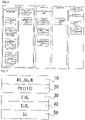
- these electronic devices include a layered structure shown in FIG. 1 .
- M is a metal (conductor)
- F is a ferroelectric body
- S is a semiconductor
- I an insulator
- AF antiferroelectric body.
- these electronic devices include a ferroelectric layer (F) that is formed on a metal (conductor) layer (M), a semiconductor layer (S), or an insulator layer (I).
- the electronic device that is more compact and have higher performance than conventional electronic devices since the aforementioned ferroelectric thin film has very high ferroelectric properties and high stability.
- a sixteenth aspect of the present invention is a method for producing the ferroelectric thin film according to any one of the first to fourteenth aspects by a sputtering method, wherein a sputtering gas contains at least nitrogen, a molar concentration of nitrogen contained in the sputtering gas is within the range of 0.667 to 1.0, and a pressure of the sputtering gas is 1 Pa or less.
- the "sputtering gas” refers to a gas used in the sputtering method.
- the sputtering gas include inert gases such as nitrogen (N 2 ) and argon (Ar).
- a ferroelectric thin film having a high remanent polarization value can be produced without causing dielectric breakdown even when a high electric field is applied.
- FIG. 2 is a schematic side view of a ferroelectric thin film according to a first embodiment.
- a ferroelectric thin film 10 is formed on a thin film composed of three layers, a silicon dioxide layer (SiO 2 layer) 40, a titanium dioxide layer (TiO 2 layer) 30, and a platinum (111) layer (Pt(111) layer) 20 laminated in this order from the bottom to the top on a silicon substrate (Si substrate) 50.
- the Pt(111) layer refers to a platinum layer having a Miller index of (111).
- the Si substrate 50 is not particularly limited, and a commercially available Si substrate can be used.
- the thickness of the Si substrate is not particularly limited.
- the SiO 2 layer 40 is also not particularly limited as long as it can be formed by sputtering or the like.
- the thickness of the SiO 2 layer is not particularly limited as long as it is within the range of 10 nm to 2,000 nm.
- the TiO 2 layer 30 is also not particularly limited as long as it can be formed by sputtering or the like.
- the thickness of the TiO 2 layer is not particularly limited as long as it is within the range of 2 nm to 100 nm.
- a tantalum layer, a tantalum oxide layer, a niobium layer, a niobium oxide layer, or the like may be used.
- the Pt(111) layer 20 is also not particularly limited as long as it can be formed by sputtering or the like.
- the thickness of the Pt(111) layer is not particularly limited as long as it is within the range of 20 nm to 200 nm.
- the ferroelectric thin film 10 formed on the Pt(111) layer 20 includes scandium(Sc)-doped aluminum nitride represented by the chemical formula of Al 1-x Sc x N.
- X is a Sc concentration.
- the ferroelectric thin film 10 has X that is within the range higher than 0 and 0.219 or lower.
- the Sc concentration X of the ferroelectric thin film 10 is lower than the Sc concentration at which it is recognized that the thin film cannot be formed.
- the ferroelectric thin film 10 has much higher ferroelectric properties and higher stability than the ferroelectric thin film including Al 1-X Sc X N disclosed in Non-Patent Literature 1.
- the thickness of the ferroelectric thin film 10 is not particularly limited, and is preferably within the range of 1 nm to 300 nm.
- the ferroelectric thin film 10 has sufficient ferroelectric properties and sufficiently high stability even when it is as thin as described above.
- the thickness of the ferroelectric thin film 10 is more preferably within the range of 1 nm to 200 nm.
- the ferroelectric thin film 10 has sufficient ferroelectric properties and sufficiently high stability even when it is as thin as described above.
- the thickness of the ferroelectric thin film 10 is further preferably within the range of 1 nm to 100 nm.
- the ferroelectric thin film 10 has sufficient ferroelectric properties and sufficiently high stability even when it is as thin as described above.
- the thickness of the ferroelectric thin film 10 is particularly preferably within the range of 20 nm to 80 nm.
- the ferroelectric thin film 10 has sufficient ferroelectric properties and sufficiently high stability even when it is as thin as described above.
- An electronic device using the ferroelectric thin film 10 has sufficient ferroelectric properties and sufficiently high stability, and thus the electronic device is more compact and has higher performance than conventional electronic devices.
- the configuration of such an electronic device is not particularly limited, and the electronic device can be produced by a known technique.
- the ferroelectric thin film 10 is formed on a thin film composed of three layers, the SiO 2 layer 40, the TiO 2 layer 30, and the Pt(111) layer 20 laminated in this order from the bottom to the top, on the Si substrate 50.
- the SiO 2 layer 40 is first formed on the Si substrate 50.
- a method for forming the SiO 2 layer 40 is not particularly limited.
- the SiO 2 layer 40 can be produced by a known technique such as a sputtering method, a physical vapor deposition method (PVD method), a chemical vapor deposition method (CVD method), a molecular beam epitaxy method (MBE method), a pulsed laser deposition method (PLD method), or an oxidation method (thermal oxidation, steam oxidation, etc.).
- the TiO 2 layer 30 is formed on the SiO 2 layer 40.
- a method for forming the TiO 2 layer 30 is not particularly limited.
- the TiO 2 layer 30 can be produced by a known technique such as a sputtering method, a physical vapor deposition method (PVD method), a chemical vapor deposition method (CVD method), a molecular beam epitaxy method (MBE method), a pulsed laser deposition method (PLD method), or an oxidation method (thermal oxidation, steam oxidation, etc.).
- the Pt(111) layer 20 is then formed on the formed TiO 2 layer 30.
- a method for forming the Pt(111) layer 20 is not particularly limited.
- the Pt(111) layer 20 can be produced by a known technique such as a sputtering method, a physical vapor deposition method (PVD method), or a chemical vapor deposition method (CVD method).
- the ferroelectric thin film 10 represented by the chemical formula Al 1-x Sc x N is formed on the formed Pt(111) layer 20.
- the ferroelectric thin film 10 can be formed by a general sputtering method, a physical vapor deposition method (PVD method), a chemical vapor deposition method (CVD method), a molecular beam epitaxy method (MBE method), a pulsed laser deposition method (PLD method), or the like.
- the ferroelectric thin film 10 can be produced on the Pt(111) layer 20 by simultaneously sputtering a Sc target and an Al target in a nitrogen gas (N 2 ) atmosphere or a mixed atmosphere of N 2 and argon gas (Ar) (the gas pressure may be 1 Pa or less, and preferably between 0.267 Pa and 6.67 Pa).
- N 2 nitrogen gas
- Ar argon gas
- the targets an alloy containing Sc and Al at a predetermined ratio may be used.
- the ferroelectric thin film 10 according to the present embodiment can be formed directly on the Si substrate by a production method such as a sputtering method or deposition (production method 2) as follows.
- the ferroelectric thin film 10 can be produced on the substrate (for example, a silicon (Si) substrate) by simultaneously sputtering a Sc target and an Al target in a N 2 atmosphere or a mixed atmosphere of N 2 and Ar (the gas pressure may be 1 Pa or less, and preferably between 0.10 Pa and 0.70 Pa).
- the targets an alloy containing Sc and Al at a predetermined ratio may be used.
- Examples 1 to 5 and Comparative Examples 1 to 10 The following sputtering targets and the like were used for a sputtering apparatus.
- a SiO 2 layer having a thickness of 50 nm to 200 nm, a TiO 2 layer having a thickness of 5 nm to 50 nm, a Pt(111) layer having a thickness of 50 nm to 200 nm, and a ferroelectric thin film having a thickness of 123 nm to 251 nm were produced multiple times by the aforementioned production method 1.
- the ferroelectric thin films each had different Sc concentrations X.
- a ferroelectric thin film having a thickness of 290 nm to 460 nm was produced multiple times by the aforementioned production method 2.
- the ferroelectric thin films each had different Sc concentrations X.
- the air pressure inside the sputtering chamber was reduced to a high vacuum of 10 -6 Pa or lower using a vacuum pump. Furthermore, a target surface was subjected to a cleaning treatment immediately after installation of the targets and immediately before each film forming experiment to prevent contamination by impurities such as oxygen.
- a Pt electrode was provided on each of the ferroelectric thin films. Electric field-polarization characteristics of the respective ferroelectric thin films shown in FIG. 3 were measured using FCE-1/1A (manufactured by TOYO Corporation).
- FIGs. 4 to 8 illustrate the measurement results. As can be seen from FIGs. 4 to 8 , the ferroelectric thin films in Examples 1 to 5 exhibit a clear hysteresis curve.
- the ferroelectric thin films in Examples 1 to 3 and 5, and Comparative Examples 6 and 7 were each subjected to measurement by a Positive-Up-Negative-Down (PUND) method.
- PUND Positive-Up-Negative-Down
- a negative electric field waveform was applied once, a positive electric field waveform was applied twice, and a negative electric field waveform was then applied twice to the ferroelectric thin films in Examples 1 to 3 and 5, and Comparative Examples 6 and 7 to measure a polarization reversal.
- FIG. 9 illustrates the result.
- a black filled circle represents Example 1
- an open square represents Example 2
- an open triangle represents Example 3
- an open circle represents Example 5
- a black filled inverted triangle represents Comparative Example 6
- a black filled square represents Comparative Example 7.
- a lower Sc concentration exhibits a higher remanent polarization value (Pr).
- FIG. 10 is a graph showing the relationship between the Sc concentration X and Pr of the ferroelectric thin films.
- data represented by black filled circles indicate data of the ferroelectric thin films produced by the production method 1 or 2
- data represented by black filled triangles indicate numerical values described in Non-Patent Literature 1.
- the remanent polarization values (Pr) of the ferroelectric thin films (Examples 1 to 5) having a Sc concentration of 0.065 or more and 0.219 or less are higher than those of the ferroelectric thin films (Comparative Examples 1 to 8) having a Sc concentration between 0.27 and 0.49.
- aluminum nitride (Al 1-x Sc x N) having a doped Sc concentration X of 0.065 or more and 0.219 or less has a higher remanent polarization value (Pr) than aluminum nitride having a doped Sc concentration X between 0.27 and 0.49.
- FIG. 11 is a graph showing the relationship between u and Pr for a section of each of the ferroelectric thin films shown in FIG. 3 .
- u refers to a ratio between a lattice constant in a polarization direction and the average distance between nitrogen atoms and metal atoms such as Al.
- a is an a-axis lattice constant
- c is a c-axis lattice constant
- the ferroelectric thin film having u of 0.375 or more and less than 0.5 has a high remanent polarization value (Pr) as described above.
- the ferroelectric thin film having u of 0.375 or more and less than 0.5 has a high remanent polarization value regardless of its crystal structure.
- the ferroelectric thin film having u of 0.382 or more and 0.5 or less is more preferable since a high Pr is surely achieved.
- the ferroelectric thin film having u of 0.383 or more and 0.396 or less is further preferable since a high Pr is more surely achieved.
- the ferroelectric thin film having u of 0.383 or more and 0.387 or less is particularly preferable since a high Pr is further surely achieved. All the ferroelectric thin films in the present invention satisfy these relationships.
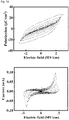
- Examples 6 to 8 In order to confirm that the ferroelectric thin film having a small thickness according to the embodiment has sufficient ferroelectric properties, ferroelectric thin films each having a smaller thickness were produced using the aforementioned production method 2. A Pt electrode was provided on each of the ferroelectric thin films. A hysteresis curve and a current relative to an electric field strength of the respective ferroelectric thin films shown in FIG. 12 were each measured using FCE-1/1A (manufactured by TOYO Corporation).
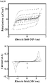
- the upper graphs of FIGs. 13 to 15 show hysteresis curves of the respective ferroelectric thin films, and the lower graphs of FIGs. 13 to 15 show the current graphs relative to the electric field strength.
- the ferroelectric thin films in Examples 6 to 8 have ferroelectric properties.
- the ferroelectric thin films were produced using a process at higher temperatures.
- the present invention is not limited to the embodiment.
- the ferroelectric thin film according to the present invention can be produced even when the heating temperature of a substrate (base material) in the aforementioned production methods is low (for example, in the range of 20°C to 30°C).
- the ferroelectric thin film according to the present invention can be formed on a low-heat resistant base material which is a base material having low heat resistance.
- the ferroelectric thin film according to the present invention can be used in an electronic device having low heat resistance.
- the low-heat resistant base material include soda-lime glass, organic base materials (polyethylene terephthalate (PET)), polyimide, and alkali-free glass.
- Examples 9 to 13 The following sputtering targets and the like were used for a sputtering apparatus.
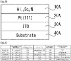
- a base material (substrate) 40A an indium tin oxide (ITO) layer 30A having a thickness of 50 nm to 200 nm, a Pt(111) layer 20A having a thickness of 50 nm to 200 nm, and a ferroelectric thin film 10A having a thickness of 138 nm to 145 nm were produced multiple times as shown in FIG. 16 .
- ITO indium tin oxide
- the air pressure inside a sputtering chamber was reduced to a high vacuum of 10 -6 Pa or lower using a vacuum pump, like Examples and Comparative Examples described above. Furthermore, a target surface was subjected to a cleaning treatment immediately after installation of the targets and immediately before each film forming experiment to prevent contamination by impurities such as oxygen.
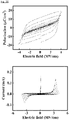
- FIG. 18 to 22 illustrate the measurement results. As can be seen from FIGs. 18 to 22 , the ferroelectric thin films each exhibit a clear hysteresis curve. Therefore, the ferroelectric thin films each have ferroelectric properties.
- the ferroelectric thin film is described using an example of Sc-doped aluminum nitride (Al 1-x Sc x N).
- Al 1-x Sc x N Sc-doped aluminum nitride
- the present invention is not limited to the embodiments.
- the ferroelectric thin film according to the present invention include Al 1-X (Mg 1-Y Nb Y ) X N (0 ⁇ X ⁇ 1, 0 ⁇ Y ⁇ 1).
- Such a ferroelectric thin film is more inexpensive and has high ferroelectric properties and high stability.
- X is preferably within the range of 0.01 or more and 0.7 or less, and Y is preferably within the range of 0 or more and 1 or less. X is more preferably within the range of more than 0.01 and 0.7 or less, and Y is more preferably within the range of more than 0 and less than 1.0.
- a ferroelectric thin film (Al 1-X (Mg 1-Y Nb Y ) X N) having X and Y falling within such ranges is more inexpensive and has higher ferroelectric properties and higher stability.
- X is more preferably within the range of 0.57 or more and 0.63 or less, and Y is more preferably within the range of 0.365 or more and 0.532 or less.
- a ferroelectric thin film (Al 1-X (Mg 1-Y Nb Y ) X N) having X and Y falling within such ranges has further higher ferroelectric properties and further higher stability.
- ferroelectric thin film examples include Al 1-X Yb X N (0 ⁇ X ⁇ 1). Such a ferroelectric thin film is more inexpensive and has high ferroelectric properties and high stability.
- X is preferably within the range of more than 0 and less than 1, and more preferably within the range of 0.01 or more and 0.8 or less.
- a ferroelectric thin film (Al 1-X Yb X N) having X falling within such a range is more inexpensive and has higher ferroelectric properties and higher stability.
- X is more preferably within the range of 0.25 or more and 0.282 or less.
- a ferroelectric thin film (Al 1-X Yb X N) having X falling within such a range has further higher ferroelectric properties and further higher stability.
- ferroelectric thin film according to the present invention examples include Ga 1- xScxN (0 ⁇ X ⁇ 1). Such a ferroelectric thin film has high ferroelectric properties and high stability.
- X is preferably within the range of 0 or more and less than 1, more preferably within the range of more than 0 and less than 1, further preferably within the range of 0 or more and 0.50 or less, and particularly preferably within the range of more than 0 and 0.50 or less.
- a ferroelectric thin film (Ga 1-X Sc X N) having X falling within such a range has higher ferroelectric properties and higher stability.
- X is more preferably within the range of 0 or more and 0.41 or less, and particularly preferably within the range of more than 0 and 0.41 or less.
- a ferroelectric thin film (Ga 1-X Sc X N) having X falling within such a range has further higher ferroelectric properties and further higher stability.
- ferroelectric thin film according to the present invention examples include GaN. Such a ferroelectric thin film has high ferroelectric properties and high stability.
- ferroelectric thin films described above can be actually produced using the same production method as that in the first embodiment.
- Examples 14 to 24 Thin films shown in FIG. 23 were produced on a substrate (Si, Hf, Ti) by the aforementioned film-forming method.
- a “laminating order” indicates an order of laminating each film on the substrate.
- the laminating order means that layers are laminated in turn from a right layer to a left layer.
- Al 0.37 Mg 0.4 Nb 0.23 N/Si means that an Al 0.37 Mg 0.4 Nb 0.23 N layer is formed on an Si substrate.
- a “ferroelectric layer thickness” refers to the thickness of each corresponding layer.
- FIG. 24 to 34 illustrate the measurement results. As can be seen from FIGs. 24 to 34 , the ferroelectric thin films each exhibit a clear hysteresis curve. Therefore, the ferroelectric thin films each have ferroelectric properties.
- the type and the pressure of sputtering gas used in the sputtering method are not particularly limited.
- a ferroelectric thin film having a higher remanent polarization value (Pr) can be provided.
- a gas other than nitrogen contained in the sputtering gas is not particularly limited as long as it is an inert gas.
- Examples 25 to 27 The following sputtering targets and the like were used for a sputtering apparatus. On each of three n-type Si substrates each having a specific resistance of 0.02 Qcm, a SiO 2 layer having a thickness of 50 nm to 200 nm, a TiO 2 layer having a thickness of 5 nm to 50 nm, and a Pt(111) layer having a thickness of 50 nm to 200 nm were formed, and a ferroelectric thin film (Al 1-x Sc x N) shown in FIG. 35 was produced by the aforementioned production method 1. Note that during film forming, the molar concentration of nitrogen and the molar concentration of argon contained in the sputtering gas were only changed as shown in FIG. 36 .
- FIG. 37 illustrates the results.
- a black filled circle represents Example 25
- an open rhombus represents Example 26
- a black filled inverted triangle represents Example 27.
- the remanent polarization value (Pr) is higher.
- FIG. 38 illustrates the results.
- the leakage current density in Example 27 could not be measured under application of an electric field of 2.20 MV/cm or more since dielectric breakdown occurred under application of an electric field strength of 2.20 MV/cm.
- the leakage current density in Example 26 abruptly increased under application of an electric field strength of higher than 2.75 MV/cm, but dielectric breakdown did not occur.
- Example 25 the leakage current density in Example 25 was lower than that in Example 26, and dielectric breakdown did not occur. From the results of Examples 25 and 26, it is considered that for the ferroelectric thin film produced using the sputtering gas in which the molar concentration of nitrogen is within the range of 0.667 to 1.0, dielectric breakdown does not occur even when an electric field strength of 2.20 MV/cm or more is applied. Note that under a condition where the pressure of the sputtering gas is 1 Pa or less, a ferroelectric thin film similar to the ferroelectric thin films is obtained.
- a ferroelectric thin film having a high remanent polarization value can be produced without causing dielectric breakdown even when a high electric field strength is applied.
Landscapes
- Chemical & Material Sciences (AREA)
- Organic Chemistry (AREA)
- Engineering & Computer Science (AREA)
- Materials Engineering (AREA)
- Ceramic Engineering (AREA)
- Inorganic Chemistry (AREA)
- Metallurgy (AREA)
- Manufacturing & Machinery (AREA)
- Mechanical Engineering (AREA)
- Chemical Kinetics & Catalysis (AREA)
- Structural Engineering (AREA)
- Crystallography & Structural Chemistry (AREA)
- Life Sciences & Earth Sciences (AREA)
- Geology (AREA)
- Analytical Chemistry (AREA)
- Computer Hardware Design (AREA)
- Inorganic Insulating Materials (AREA)
- Semiconductor Memories (AREA)
- Physical Vapour Deposition (AREA)
- Formation Of Insulating Films (AREA)
- Physical Deposition Of Substances That Are Components Of Semiconductor Devices (AREA)
Abstract
Description
- The present invention relates to a ferroelectric thin film, an electronic device using the same, and a method for producing the ferroelectric thin film.
- Already known ferroelectric materials are barium titanate (BaTiO3), lead zirconate titanate (Pb(Zr, Ti)O3), lead lanthanum zirconate titanate ((Pb, La)(Zr, Ti)O3), bismuth ferrate (BiFeO3), and the like. Ferroelectric bodies (ferroelectric thin films), a kind of dielectric body, refer to a substance in which electric dipoles are aligned in the absence of an external electric field and directions of the dipoles can vary depending on the electric field. Such ferroelectric bodies are a dielectric body having pyroelectric properties and piezoelectric properties in addition to ferroelectric properties. Thus, the ferroelectric bodies are used as a ferroelectric random access memory (FeRAM) or the like that uses ferroelectric properties, or as an actuator or the like that uses the piezoelectric effect.
- Among ferroelectric materials, scandium-doped aluminum nitride having excellent ferroelectric properties has been recently reported (see Non-Patent Literature 1).
- Non-Patent Literature 1: Simon Fichtner, Niklas Wolff, Fabian Lofink, Lorenz Kienle, and Bernhard Wagner, J. Appl. Phys. 125, 114103(2019)
-
Non-Patent Literature 1 describes that when the concentration X of scandium (Sc) in Sc-doped aluminum nitride (Al1-xScxN) is lower than 0.22, dielectric breakdown occurs before an electric field reaches a coercive electric field. - Therefore, there is a problem in which a ferroelectric thin film cannot be formed from Al1-xScxN having a Sc concentration X lower than 0.22.
- A ferroelectric thin film including Al1-xScxN has a problem in which when a sufficient thickness (for example, 600 nm or more) of the ferroelectric thin film is not available, the ferroelectric thin film exhibits insufficient ferroelectric properties and lacks stability when applied to practical use.
- In view of the circumstances described above, it is an object of the present invention to provide a ferroelectric thin film having high ferroelectric properties and stability when applied to practical use, an electronic device using the same, and a method for producing the ferroelectric thin film.
- The inventors of the present invention have intensively performed research and development on the aforementioned problems, and as a result found a ferroelectric thin film that is innovative as described below, an electronic device using the same, and a method for producing the ferroelectric thin film.
- A first aspect of the present invention to solve the problems is a ferroelectric thin film represented by a chemical formula M11-XM2XN, wherein M1 is at least one element selected from aluminum (Al) and gallium (Ga), M2 is at least one element selected from magnesium (Mg), scandium (Sc), ytterbium (Yb), and niobium (Nb), and X is within the range of 0 or more and 1 or less.
- In the first aspect, the ferroelectric thin film that has high ferroelectric properties and high stability can be provided.
- A second aspect of the present invention is the ferroelectric thin film according to the first aspect, wherein M1 is Al, M2 is Sc, and X is within the range of more than 0 and 0.219 or less.
- In the second aspect, there can be provided the ferroelectric thin film that has much higher ferroelectric properties and higher stability than the ferroelectric thin film including Al1-xScxN disclosed in
Non-Patent Literature 1 although the Sc concentration is lower than the Sc concentration at which it is recognized that the thin film cannot be formed. - A third aspect of the present invention is the ferroelectric thin film according to the first aspect, wherein M1 is Al, M2 is Sc, and X is within the range of 0.065 or more and 0.219 or less.
- In the third aspect, there can be provided the ferroelectric thin film that has much higher ferroelectric properties and higher stability than the ferroelectric thin film including Al1-xScxN disclosed in
Non-Patent Literature 1 although the Sc concentration is lower than the Sc concentration at which it is recognized that the thin film cannot be formed. - A fourth aspect of the present invention is the ferroelectric thin film according to the first aspect, wherein M1 is Al, M2 is Sc, and X is within the range of 0.16 or more and 0.219 or less.
- In the fourth aspect, there can be provided the ferroelectric thin film that has much higher ferroelectric properties and higher stability than the ferroelectric thin film including Al1-xScxN disclosed in
Non-Patent Literature 1 although the Sc concentration is lower than the Sc concentration at which it is recognized that the thin film cannot be formed. - A fifth aspect of the present invention is the ferroelectric thin film according to the first aspect, wherein M1 is Al, M2 is Mg1-YNbY, X is within the range of 0 or more and 1 or less, and Y is within the range of 0 or more and 1 or less.
- In the fifth aspect, the ferroelectric thin film that is more inexpensive and have higher ferroelectric properties and higher stability can be provided.
- A sixth aspect of the present invention is the ferroelectric thin film according to the first aspect, wherein M1 is Ga, M2 is Sc, and X is within the range of 0 or more and 1 or less.
- In the sixth aspect, the ferroelectric thin film that has higher ferroelectric properties and higher stability can be provided. This aspect is highly applicable to current gallium nitride semiconductors and their production processes, and a production process of this aspect can easily be incorporated into the production processes for the current gallium nitride semiconductors.
- A seventh aspect of the present invention is the ferroelectric thin film according to the first aspect, wherein M1 is Al, M2 is Yb, and X is within the range of 0 or more and 1 or less.
- In the seventh aspect, the ferroelectric thin film that has higher ferroelectric properties and higher stability can be provided.
- An eighth aspect of the present invention is the ferroelectric thin film according to the first aspect, wherein M1 is Ga, and X is 0.
- In the eighth aspect, the ferroelectric thin film that has higher ferroelectric properties and higher stability can be provided. This aspect is highly applicable to the current gallium nitride semiconductors and their production processes, and a production process of this aspect can easily be incorporated into the production processes for the current gallium nitride semiconductors.
- A ninth aspect of the present invention is the ferroelectric thin film according to any one of the first to eighth aspects, wherein u calculated by the following expression is within the range of 0.375 or more and less than 0.5.

- In the ninth aspect, the ferroelectric thin film that has a higher remanent polarization value (Pr) can be provided.
- A tenth aspect of the present invention is the ferroelectric thin film according to any one of the first to ninth aspects having a thickness of 1 nm to 300 nm.
- In the tenth aspect, there can be provided the ferroelectric thin film that has sufficient ferroelectric properties and sufficiently high stability without deteriorating characteristics even when the film thickness is small as described above.
- An eleventh aspect of the present invention is the ferroelectric thin film according to any one of the first to ninth aspects having a thickness of 1 nm to 200 nm.
- In the eleventh aspect, there can be provided the ferroelectric thin film that has sufficient ferroelectric properties and sufficiently high stability without deteriorating characteristics even when the film thickness is smaller as described above.
- A twelfth aspect of the present invention is the ferroelectric thin film according to any one of the first to ninth aspects having a thickness of 1 nm to 100 nm.
- In the twelfth aspect, there can be provided the ferroelectric thin film that has sufficient ferroelectric properties and sufficiently high stability without deteriorating characteristics even when the film thickness is further smaller.
- A thirteenth aspect of the present invention is the ferroelectric thin film according to any one of the first to ninth aspects having a thickness of 20 nm to 80 nm.
- In the thirteenth aspect, there can be provided the ferroelectric thin film that has sufficient ferroelectric properties and sufficiently high stability without deteriorating characteristics even when the film thickness is small as described above.
- A fourteenth aspect of the present invention is a ferroelectric thin film including the ferroelectric thin film according to any one of the first to thirteenth aspects which is provided on a low-heat resistant base material.
- Herein, the low-heat resistant base material is not particularly limited as long as it is a base material having low heat resistance (a material having an upper limit of usable temperature of 50°C to 700°C). Examples of the low-heat resistant base material include soda-lime glass, organic base materials (polyethylene terephthalate (PET)), polyimide, and alkali-free glass.
- In the fourteenth aspect, the ferroelectric thin film according to the present invention can be produced even when the heating temperature of a substrate (base material) is low (for example, 20°C to 30°C). Thus, a flexible device or a display memory, for example, can be produced with the use of the ferroelectric thin film according to the present invention.
- A fifteenth aspect of the present invention is an electronic device using the ferroelectric thin film according to any one of the first to fourteenth aspects.
- Here, the "electronic device" is a device including a ferroelectric nonvolatile memory (including an electric field effect ferroelectric nonvolatile memory), a resistance-variable nonvolatile memory, a piezoresistance transistor, an energy storage device, a piezoelectric device (piezoelectric element), a pyroelectric device, a piezoelectric sensor, and an electrocaloric effect device. For example, these electronic devices include a layered structure shown in
FIG. 1 . InFIG. 1 , M is a metal (conductor), F is a ferroelectric body, S is a semiconductor, I is an insulator, and AF is an antiferroelectric body. As can be seen fromFIG. 1 , these electronic devices include a ferroelectric layer (F) that is formed on a metal (conductor) layer (M), a semiconductor layer (S), or an insulator layer (I). - In the fifteenth aspect, there can be provided the electronic device that is more compact and have higher performance than conventional electronic devices since the aforementioned ferroelectric thin film has very high ferroelectric properties and high stability.
- A sixteenth aspect of the present invention is a method for producing the ferroelectric thin film according to any one of the first to fourteenth aspects by a sputtering method, wherein a sputtering gas contains at least nitrogen, a molar concentration of nitrogen contained in the sputtering gas is within the range of 0.667 to 1.0, and a pressure of the sputtering gas is 1 Pa or less.
- Here, the "sputtering gas" refers to a gas used in the sputtering method. Examples of the sputtering gas include inert gases such as nitrogen (N2) and argon (Ar).
- According to the sixteenth aspect, a ferroelectric thin film having a high remanent polarization value can be produced without causing dielectric breakdown even when a high electric field is applied.
-
-
FIG. 1 is a conceptual side view of a layered structure of an electronic device according to the present invention as an example. -
FIG. 2 is a schematic side view of a ferroelectric thin film according to a first embodiment. -
FIG. 3 is a table showing components and production methods in Examples 1 to 5 and Comparative Examples. -
FIG. 4 is a graph showing a hysteresis curve in Example 1. -
FIG. 5 is a graph showing a hysteresis curve in Example 2. -
FIG. 6 is a graph showing a hysteresis curve in Example 3. -
FIG. 7 is a graph showing a hysteresis curve in Example 4. -
FIG. 8 is a graph showing a hysteresis curve in Example 5. -
FIG. 9 is a graph showing results of PUND measurement in Examples 1 to 3 and 5, and Comparative Examples 6 and 7. -
FIG. 10 is a graph showing a relationship between a concentration X of Sc and a remanent polarization value (Pr) in Examples and Comparative Examples. -
FIG. 11 is a graph showing a relationship between u and Pr. -
FIG. 12 is a table showing components and film thickness in Examples 6 to 8. -
FIG. 13 includes graphs showing a hysteresis curve (upper graph) and a relationship between an electric field strength and a current (lower graph) in Example 6. -
FIG. 14 includes graphs showing a hysteresis curve (upper graph) and a relationship between an electric field strength and a current (lower graph) in Example 7. -
FIG. 15 includes graphs showing a hysteresis curve (upper graph) and a relationship between an electric field strength and a current (lower graph) in Example 8. -
FIG. 16 is a schematic side view of a ferroelectric thin film according to a second embodiment. -
FIG. 17 is a table showing Examples 9 to 13 and structures of thin films in Examples 9 to 13. -
FIG. 18 includes graphs showing a hysteresis curve (upper graph) and a relationship between an electric field strength and a current (lower graph) in Example 9. -
FIG. 19 includes graphs showing a hysteresis curve (upper graph) and a relationship between an electric field strength and a current (lower graph) in Example 10. -
FIG. 20 includes graphs showing a hysteresis curve (upper graph) and a relationship between an electric field strength and a current (lower graph) in Example 11. -
FIG. 21 includes graphs showing a hysteresis curve (upper graph) and a relationship between an electric field strength and a current (lower graph) in Example 12. -
FIG. 22 includes graphs showing a hysteresis curve (upper graph) and a relationship between an electric field strength and a current (lower graph) in Example 13. -
FIG. 23 is a table showing Examples 14 to 24 and structures of thin films in Examples 14 to 24. -
FIG. 24 includes graphs showing a hysteresis curve (upper graph) and a relationship between an electric field strength and a current (lower graph) in Example 14. -
FIG. 25 includes graphs showing a hysteresis curve (upper graph) and a relationship between an electric field strength and a current (lower graph) in Example 15. -
FIG. 26 includes graphs showing a hysteresis curve (upper graph) and a relationship between an electric field strength and a current (lower graph) in Example 16. -
FIG. 27 includes graphs showing a hysteresis curve (upper graph) and a relationship between an electric field strength and a current (lower graph) in Example 17. -
FIG. 28 includes graphs showing a hysteresis curve (upper graph) and a relationship between an electric field strength and a current (lower graph) in Example 18. -
FIG. 29 includes graphs showing a hysteresis curve (upper graph) and a relationship between an electric field strength and a current (lower graph) in Example 19. -
FIG. 30 includes graphs showing a hysteresis curve (upper graph) and a relationship between an electric field strength and a current (lower graph) in Example 20. -
FIG. 31 includes graphs showing a hysteresis curve (upper graph) and a relationship between an electric field strength and a current (lower graph) in Example 21. -
FIG. 32 includes graphs showing a hysteresis curve (upper graph) and a relationship between an electric field strength and a current (lower graph) in Example 22. -
FIG. 33 includes graphs showing a hysteresis curve (upper graph) and a relationship between an electric field strength and a current (lower graph) in Example 23. -
FIG. 34 includes graphs showing a hysteresis curve (upper graph) and a relationship between an electric field strength and a current (lower graph) in Example 24. -
FIG. 35 is a table showing structures in Examples 25 to 27. -
FIG. 36 is a table showing the molar concentration of each gas contained in sputtering gases used during production of Examples 25 to 27. -
FIG. 37 is a graph showing a relationship between an electric field strength and a remanent polarization value (Pr) in ferroelectric thin films produced using the respective sputtering gases. -
FIG. 38 is a graph showing a relationship between an electric field strength and a leakage current density in ferroelectric thin films produced using the respective sputtering gases. - Hereinafter, embodiments of a ferroelectric thin film according to the present invention will be described with reference to the accompanying drawings. The present invention is not limited to the following embodiments.
-
FIG. 2 is a schematic side view of a ferroelectric thin film according to a first embodiment. As shown inFIG. 2 , a ferroelectricthin film 10 is formed on a thin film composed of three layers, a silicon dioxide layer (SiO2 layer) 40, a titanium dioxide layer (TiO2 layer) 30, and a platinum (111) layer (Pt(111) layer) 20 laminated in this order from the bottom to the top on a silicon substrate (Si substrate) 50. Herein, the Pt(111) layer refers to a platinum layer having a Miller index of (111). - The
Si substrate 50 is not particularly limited, and a commercially available Si substrate can be used. The thickness of the Si substrate is not particularly limited. - The SiO2 layer 40 is also not particularly limited as long as it can be formed by sputtering or the like. The thickness of the SiO2 layer is not particularly limited as long as it is within the range of 10 nm to 2,000 nm.
- The TiO2 layer 30 is also not particularly limited as long as it can be formed by sputtering or the like. The thickness of the TiO2 layer is not particularly limited as long as it is within the range of 2 nm to 100 nm. Instead of the TiO2 layer, a tantalum layer, a tantalum oxide layer, a niobium layer, a niobium oxide layer, or the like may be used.
- The Pt(111)
layer 20 is also not particularly limited as long as it can be formed by sputtering or the like. The thickness of the Pt(111) layer is not particularly limited as long as it is within the range of 20 nm to 200 nm. - The ferroelectric
thin film 10 formed on the Pt(111)layer 20 includes scandium(Sc)-doped aluminum nitride represented by the chemical formula of Al1-xScxN. Herein, X is a Sc concentration. The ferroelectricthin film 10 has X that is within the range higher than 0 and 0.219 or lower. - The Sc concentration X of the ferroelectric
thin film 10 is lower than the Sc concentration at which it is recognized that the thin film cannot be formed. However, the ferroelectricthin film 10 has much higher ferroelectric properties and higher stability than the ferroelectric thin film including Al1-XScXN disclosed inNon-Patent Literature 1. - Herein, the thickness of the ferroelectric
thin film 10 is not particularly limited, and is preferably within the range of 1 nm to 300 nm. The ferroelectricthin film 10 has sufficient ferroelectric properties and sufficiently high stability even when it is as thin as described above. - The thickness of the ferroelectric
thin film 10 is more preferably within the range of 1 nm to 200 nm. The ferroelectricthin film 10 has sufficient ferroelectric properties and sufficiently high stability even when it is as thin as described above. - The thickness of the ferroelectric
thin film 10 is further preferably within the range of 1 nm to 100 nm. The ferroelectricthin film 10 has sufficient ferroelectric properties and sufficiently high stability even when it is as thin as described above. - The thickness of the ferroelectric
thin film 10 is particularly preferably within the range of 20 nm to 80 nm. The ferroelectricthin film 10 has sufficient ferroelectric properties and sufficiently high stability even when it is as thin as described above. - An electronic device using the ferroelectric
thin film 10 has sufficient ferroelectric properties and sufficiently high stability, and thus the electronic device is more compact and has higher performance than conventional electronic devices. The configuration of such an electronic device is not particularly limited, and the electronic device can be produced by a known technique. - Next, a method for producing the ferroelectric
thin film 10 according to the present embodiment (production method 1) will be described. As described above, the ferroelectricthin film 10 is formed on a thin film composed of three layers, the SiO2 layer 40, the TiO2 layer 30, and the Pt(111)layer 20 laminated in this order from the bottom to the top, on theSi substrate 50. - The SiO2 layer 40 is first formed on the
Si substrate 50. A method for forming the SiO2 layer 40 is not particularly limited. The SiO2 layer 40 can be produced by a known technique such as a sputtering method, a physical vapor deposition method (PVD method), a chemical vapor deposition method (CVD method), a molecular beam epitaxy method (MBE method), a pulsed laser deposition method (PLD method), or an oxidation method (thermal oxidation, steam oxidation, etc.). - Subsequently, the TiO2 layer 30 is formed on the SiO2 layer 40. A method for forming the TiO2 layer 30 is not particularly limited. The TiO2 layer 30 can be produced by a known technique such as a sputtering method, a physical vapor deposition method (PVD method), a chemical vapor deposition method (CVD method), a molecular beam epitaxy method (MBE method), a pulsed laser deposition method (PLD method), or an oxidation method (thermal oxidation, steam oxidation, etc.).
- The Pt(111)
layer 20 is then formed on the formed TiO2 layer 30. A method for forming the Pt(111)layer 20 is not particularly limited. The Pt(111)layer 20 can be produced by a known technique such as a sputtering method, a physical vapor deposition method (PVD method), or a chemical vapor deposition method (CVD method). - The ferroelectric
thin film 10 represented by the chemical formula Al1-xScxN is formed on the formed Pt(111)layer 20. The ferroelectricthin film 10 can be formed by a general sputtering method, a physical vapor deposition method (PVD method), a chemical vapor deposition method (CVD method), a molecular beam epitaxy method (MBE method), a pulsed laser deposition method (PLD method), or the like. Specifically, the ferroelectricthin film 10 can be produced on the Pt(111)layer 20 by simultaneously sputtering a Sc target and an Al target in a nitrogen gas (N2) atmosphere or a mixed atmosphere of N2 and argon gas (Ar) (the gas pressure may be 1 Pa or less, and preferably between 0.267 Pa and 6.67 Pa). As the targets, an alloy containing Sc and Al at a predetermined ratio may be used. A compound containing Sc, Al, and N at a predetermined ratio, such as AIN, ScN, or AIScN, may be used. - Alternatively, similarly to a general piezoelectric thin film, the ferroelectric
thin film 10 according to the present embodiment can be formed directly on the Si substrate by a production method such as a sputtering method or deposition (production method 2) as follows. - Specifically, the ferroelectric
thin film 10 can be produced on the substrate (for example, a silicon (Si) substrate) by simultaneously sputtering a Sc target and an Al target in a N2 atmosphere or a mixed atmosphere of N2 and Ar (the gas pressure may be 1 Pa or less, and preferably between 0.10 Pa and 0.70 Pa). As the targets, an alloy containing Sc and Al at a predetermined ratio may be used. - Examples 1 to 5 and Comparative Examples 1 to 10:
The following sputtering targets and the like were used for a sputtering apparatus. On an n-type Si substrate having a specific resistance of 0.02 Qcm, a SiO2 layer having a thickness of 50 nm to 200 nm, a TiO2 layer having a thickness of 5 nm to 50 nm, a Pt(111) layer having a thickness of 50 nm to 200 nm, and a ferroelectric thin film having a thickness of 123 nm to 251 nm were produced multiple times by theaforementioned production method 1. The ferroelectric thin films each had different Sc concentrations X. - Sc sputtering target material (concentration: 99.99%)
- Al sputtering target material (concentration: 99.999%)
- Sputtering gas: N2 (purity: 99.99995% or more)
- Substrate heating temperature: 400°C to 500°C
- On an n-type Si substrate having a specific resistance of 0.02 Qcm, a ferroelectric thin film having a thickness of 290 nm to 460 nm was produced multiple times by the
aforementioned production method 2. The ferroelectric thin films each had different Sc concentrations X. - Sputtering apparatus: BC3263 (manufactured by ULVAC)
- Sc sputtering target material (concentration: 99.99%)
- Al sputtering target material (concentration: 99.999%)
- Sputtering gas: mixed gas of N2 (purity: 99.99995% or more) and Ar (purity: 99.9999% or more) (mixing ratio: 40:60)
- Substrate heating temperature: 300°C to 600°C
- Before the film forming experiments described above, the air pressure inside the sputtering chamber was reduced to a high vacuum of 10-6 Pa or lower using a vacuum pump. Furthermore, a target surface was subjected to a cleaning treatment immediately after installation of the targets and immediately before each film forming experiment to prevent contamination by impurities such as oxygen.
- A Pt electrode was provided on each of the ferroelectric thin films. Electric field-polarization characteristics of the respective ferroelectric thin films shown in
FIG. 3 were measured using FCE-1/1A (manufactured by TOYO Corporation). -
FIGs. 4 to 8 illustrate the measurement results. As can be seen fromFIGs. 4 to 8 , the ferroelectric thin films in Examples 1 to 5 exhibit a clear hysteresis curve. - The ferroelectric thin films in Examples 1 to 3 and 5, and Comparative Examples 6 and 7 were each subjected to measurement by a Positive-Up-Negative-Down (PUND) method. In the PUND method, a negative electric field waveform was applied once, a positive electric field waveform was applied twice, and a negative electric field waveform was then applied twice to the ferroelectric thin films in Examples 1 to 3 and 5, and Comparative Examples 6 and 7 to measure a polarization reversal.
-
FIG. 9 illustrates the result. InFIG. 9 , a black filled circle represents Example 1, an open square represents Example 2, an open triangle represents Example 3, an open circle represents Example 5, a black filled inverted triangle represents Comparative Example 6, and a black filled square represents Comparative Example 7. As can be seen fromFIG. 9 , a lower Sc concentration exhibits a higher remanent polarization value (Pr). -
FIG. 10 is a graph showing the relationship between the Sc concentration X and Pr of the ferroelectric thin films. Herein, data represented by black filled circles indicate data of the ferroelectric thin films produced by theproduction method Non-Patent Literature 1. - As can be seen from what is illustrated in
FIG. 9 , the remanent polarization values (Pr) of the ferroelectric thin films (Examples 1 to 5) having a Sc concentration of 0.065 or more and 0.219 or less are higher than those of the ferroelectric thin films (Comparative Examples 1 to 8) having a Sc concentration between 0.27 and 0.49. - In other words, aluminum nitride (Al1-xScxN) having a doped Sc concentration X of 0.065 or more and 0.219 or less has a higher remanent polarization value (Pr) than aluminum nitride having a doped Sc concentration X between 0.27 and 0.49.
- Furthermore,
FIG. 11 is a graph showing the relationship between u and Pr for a section of each of the ferroelectric thin films shown inFIG. 3 . Herein, u refers to a ratio between a lattice constant in a polarization direction and the average distance between nitrogen atoms and metal atoms such as Al. When a crystal structure is, for example, a wurtzite structure, u can be generally calculated from the following expression.
- In this expression, a is an a-axis lattice constant, and c is a c-axis lattice constant. Note that u, which is related to the distance between electric dipoles may strongly affect ferroelectric characteristics such as a polarization value.
- As can be seen from this graph, the ferroelectric thin film having u of 0.375 or more and less than 0.5 has a high remanent polarization value (Pr) as described above.
- The ferroelectric thin film having u of 0.375 or more and less than 0.5 has a high remanent polarization value regardless of its crystal structure. The ferroelectric thin film having u of 0.382 or more and 0.5 or less is more preferable since a high Pr is surely achieved. The ferroelectric thin film having u of 0.383 or more and 0.396 or less is further preferable since a high Pr is more surely achieved. The ferroelectric thin film having u of 0.383 or more and 0.387 or less is particularly preferable since a high Pr is further surely achieved. All the ferroelectric thin films in the present invention satisfy these relationships.
- Examples 6 to 8:
In order to confirm that the ferroelectric thin film having a small thickness according to the embodiment has sufficient ferroelectric properties, ferroelectric thin films each having a smaller thickness were produced using theaforementioned production method 2. A Pt electrode was provided on each of the ferroelectric thin films. A hysteresis curve and a current relative to an electric field strength of the respective ferroelectric thin films shown inFIG. 12 were each measured using FCE-1/1A (manufactured by TOYO Corporation). - The upper graphs of
FIGs. 13 to 15 show hysteresis curves of the respective ferroelectric thin films, and the lower graphs ofFIGs. 13 to 15 show the current graphs relative to the electric field strength. As can be seen fromFIGs. 13 to 15 , the ferroelectric thin films in Examples 6 to 8 have ferroelectric properties. - In the first embodiment, the ferroelectric thin films were produced using a process at higher temperatures. However, the present invention is not limited to the embodiment. For example, the ferroelectric thin film according to the present invention can be produced even when the heating temperature of a substrate (base material) in the aforementioned production methods is low (for example, in the range of 20°C to 30°C).
- Therefore, the ferroelectric thin film according to the present invention can be formed on a low-heat resistant base material which is a base material having low heat resistance. Thus, the ferroelectric thin film according to the present invention can be used in an electronic device having low heat resistance. Examples of the low-heat resistant base material include soda-lime glass, organic base materials (polyethylene terephthalate (PET)), polyimide, and alkali-free glass.
- Examples 9 to 13:
The following sputtering targets and the like were used for a sputtering apparatus. On a base material (substrate) 40A, an indium tin oxide (ITO)layer 30A having a thickness of 50 nm to 200 nm, a Pt(111)layer 20A having a thickness of 50 nm to 200 nm, and a ferroelectricthin film 10A having a thickness of 138 nm to 145 nm were produced multiple times as shown inFIG. 16 . - Sc sputtering target material (concentration: 99.99%)
- Al sputtering target material (concentration: 99.999%)
- Sputtering gas: N2 (purity: 99.99995% or more)
- Substrate heating temperature: 20°C to 30°C
- Before the film forming experiments described above, the air pressure inside a sputtering chamber was reduced to a high vacuum of 10-6 Pa or lower using a vacuum pump, like Examples and Comparative Examples described above. Furthermore, a target surface was subjected to a cleaning treatment immediately after installation of the targets and immediately before each film forming experiment to prevent contamination by impurities such as oxygen.
- A Pt electrode was provided on each of the ferroelectric thin films. An electric field strength was applied to the respective ferroelectric thin films shown in
FIG. 17 using FCE-1/1A (manufactured by TOYO Corporation).FIGs. 18 to 22 illustrate the measurement results. As can be seen fromFIGs. 18 to 22 , the ferroelectric thin films each exhibit a clear hysteresis curve. Therefore, the ferroelectric thin films each have ferroelectric properties. - In the aforementioned embodiments, the ferroelectric thin film is described using an example of Sc-doped aluminum nitride (Al1-xScxN). However, the present invention is not limited to the embodiments. Examples of the ferroelectric thin film according to the present invention include Al1-X(Mg1-YNbY)XN (0 ≤ X ≤ 1, 0 ≤ Y ≤ 1). Such a ferroelectric thin film is more inexpensive and has high ferroelectric properties and high stability.
- X is preferably within the range of 0.01 or more and 0.7 or less, and Y is preferably within the range of 0 or more and 1 or less. X is more preferably within the range of more than 0.01 and 0.7 or less, and Y is more preferably within the range of more than 0 and less than 1.0. A ferroelectric thin film (Al1-X(Mg1-YNbY)XN) having X and Y falling within such ranges is more inexpensive and has higher ferroelectric properties and higher stability. X is more preferably within the range of 0.57 or more and 0.63 or less, and Y is more preferably within the range of 0.365 or more and 0.532 or less. A ferroelectric thin film (Al1-X(Mg1-YNbY)XN) having X and Y falling within such ranges has further higher ferroelectric properties and further higher stability.
- Examples of the ferroelectric thin film include Al1-XYbXN (0 ≤ X ≤ 1). Such a ferroelectric thin film is more inexpensive and has high ferroelectric properties and high stability.
- X is preferably within the range of more than 0 and less than 1, and more preferably within the range of 0.01 or more and 0.8 or less. A ferroelectric thin film (Al1-XYbXN) having X falling within such a range is more inexpensive and has higher ferroelectric properties and higher stability. X is more preferably within the range of 0.25 or more and 0.282 or less. A ferroelectric thin film (Al1-XYbXN) having X falling within such a range has further higher ferroelectric properties and further higher stability.
- Examples of the ferroelectric thin film according to the present invention include Ga1-xScxN (0 ≤ X ≤ 1). Such a ferroelectric thin film has high ferroelectric properties and high stability.
- X is preferably within the range of 0 or more and less than 1, more preferably within the range of more than 0 and less than 1, further preferably within the range of 0 or more and 0.50 or less, and particularly preferably within the range of more than 0 and 0.50 or less. A ferroelectric thin film (Ga1-XScXN) having X falling within such a range has higher ferroelectric properties and higher stability. X is more preferably within the range of 0 or more and 0.41 or less, and particularly preferably within the range of more than 0 and 0.41 or less. A ferroelectric thin film (Ga1-XScXN) having X falling within such a range has further higher ferroelectric properties and further higher stability.
- Examples of the ferroelectric thin film according to the present invention include GaN. Such a ferroelectric thin film has high ferroelectric properties and high stability.
- The ferroelectric thin films described above can be actually produced using the same production method as that in the first embodiment.
- Examples 14 to 24:
Thin films shown inFIG. 23 were produced on a substrate (Si, Hf, Ti) by the aforementioned film-forming method. Herein, a "laminating order" indicates an order of laminating each film on the substrate. The laminating order means that layers are laminated in turn from a right layer to a left layer. For example, "Al0.37Mg0.4Nb0.23N/Si" means that an Al0.37Mg0.4Nb0.23N layer is formed on an Si substrate. A "ferroelectric layer thickness" refers to the thickness of each corresponding layer. - Similarly to Examples described above, a Pt electrode was provided on each of the ferroelectric thin films, an electric field strength was applied to the respective ferroelectric thin films shown in
FIG. 23 using FCE-1/1A (manufactured by TOYO Corporation).FIGs. 24 to 34 illustrate the measurement results. As can be seen fromFIGs. 24 to 34 , the ferroelectric thin films each exhibit a clear hysteresis curve. Therefore, the ferroelectric thin films each have ferroelectric properties. - In the aforementioned embodiments, the type and the pressure of sputtering gas used in the sputtering method are not particularly limited. When the molar concentration of nitrogen contained in the sputtering gas is within the range of 0.667 to 1.0 and the pressure of the sputtering gas is 1 Pa or less, a ferroelectric thin film having a higher remanent polarization value (Pr) can be provided. Note that a gas other than nitrogen contained in the sputtering gas is not particularly limited as long as it is an inert gas.
- Examples 25 to 27:
The following sputtering targets and the like were used for a sputtering apparatus. On each of three n-type Si substrates each having a specific resistance of 0.02 Qcm, a SiO2 layer having a thickness of 50 nm to 200 nm, a TiO2 layer having a thickness of 5 nm to 50 nm, and a Pt(111) layer having a thickness of 50 nm to 200 nm were formed, and a ferroelectric thin film (Al1-xScxN) shown inFIG. 35 was produced by theaforementioned production method 1. Note that during film forming, the molar concentration of nitrogen and the molar concentration of argon contained in the sputtering gas were only changed as shown inFIG. 36 . - Sc sputtering target material (concentration: 99.99%)
- Al sputtering target material (concentration: 99.999%)
- Sputtering gas: mixed gas of N2 (purity: 99.99995% or more) and Ar (purity: 99.9999% or more)
- Pressure of sputtering gas: 0.667 Pa
- For each of the obtained ferroelectric thin films, electric field-polarization characteristics were measured.
FIG. 37 illustrates the results. InFIG. 37 , a black filled circle represents Example 25, an open rhombus represents Example 26, and a black filled inverted triangle represents Example 27. As can be seen fromFIG. 37 , as the molar concentration of nitrogen contained in the sputtering gas is higher, the remanent polarization value (Pr) is higher. - A Pt electrode was provided on each of the ferroelectric thin films. An electric field strength was applied to the respective ferroelectric thin films using a direct current with FCE-1/1A (manufactured by TOYO Corporation), and a leakage current density at that time was measured.
FIG. 38 illustrates the results. As can be seen fromFIG. 38 , the leakage current density in Example 27 could not be measured under application of an electric field of 2.20 MV/cm or more since dielectric breakdown occurred under application of an electric field strength of 2.20 MV/cm. On the other hand, the leakage current density in Example 26 abruptly increased under application of an electric field strength of higher than 2.75 MV/cm, but dielectric breakdown did not occur. Similarly, the leakage current density in Example 25 was lower than that in Example 26, and dielectric breakdown did not occur. From the results of Examples 25 and 26, it is considered that for the ferroelectric thin film produced using the sputtering gas in which the molar concentration of nitrogen is within the range of 0.667 to 1.0, dielectric breakdown does not occur even when an electric field strength of 2.20 MV/cm or more is applied. Note that under a condition where the pressure of the sputtering gas is 1 Pa or less, a ferroelectric thin film similar to the ferroelectric thin films is obtained. - Therefore, by using a sputtering gas in which the molar concentration of nitrogen is within the range of 0.667 to 1.0 and the pressure is 1 Pa or less, a ferroelectric thin film having a high remanent polarization value can be produced without causing dielectric breakdown even when a high electric field strength is applied.
- It is considered that when a sputtering gas that satisfies the condition is used for production, all the ferroelectric thin films described herein can similarly have a high remanent polarization value without causing dielectric breakdown even when a high electric field strength is applied.
-
- 10, 10A
- ferroelectric thin film
- 20, 20A
- Pt(111) layer
- 30
- TiO2 layer
- 30A
- ITO layer
- 40
- SiO2 layer
- 40A
- base material (substrate)
- 50
- Si substrate
Claims (16)
- A ferroelectric thin film represented by a chemical formula M11-XM2XN, wherein M1 is at least one element selected from Al and Ga, M2 is at least one element selected from Mg, Sc, Yb, and Nb, and X is within a range of 0 or more and 1 or less.
- The ferroelectric thin film according to claim 1, wherein M1 is Al, M2 is Sc, and X is within a range of more than 0 and 0.219 or less.
- The ferroelectric thin film according to claim 1, wherein M1 is Al, M2 is Sc, and X is within a range of 0.065 or more and 0.219 or less.
- The ferroelectric thin film according to claim 1, wherein M1 is Al, M2 is Sc, and X is within a range of 0.16 or more and 0.219 or less.
- The ferroelectric thin film according to claim 1, wherein M1 is Al, M2 is Mg1-YNbY, X is within a range of 0 or more and 1 or less, and Y is within a range of 0 or more and 1 or less.
- The ferroelectric thin film according to claim 1, wherein M1 is Ga, M2 is Sc, and X is within a range of 0 or more and 1 or less.
- The ferroelectric thin film according to claim 1, wherein M1 is Al, M2 is Yb, and X is within a range of 0 or more and 1 or less.
- The ferroelectric thin film according to claim 1, wherein M1 is Ga, and X is 0.
- The ferroelectric thin film according to any one of claims 1 to 8, wherein u calculated by the following expression is within a range of 0.375 or more and less than 0.5:

- The ferroelectric thin film according to any one of claims 1 to 9, having a thickness of 1 nm to 300 nm.
- The ferroelectric thin film according to any one of claims 1 to 9, having a thickness of 1 nm to 200 nm.
- The ferroelectric thin film according to any one of claims 1 to 9, having a thickness of 1 nm to 100 nm.
- The ferroelectric thin film according to any one of claims 1 to 9, having a thickness of 20 nm to 80 nm.
- A ferroelectric thin film comprising the ferroelectric thin film according to any one of claims 1 to 13 which is provided on a low-heat resistant base material.
- An electronic device using the ferroelectric thin film according to any one of claims 1 to 14.
- A method for producing the ferroelectric thin film according to any one of claims 1 to 14 by a sputtering method, wherein:a sputtering gas contains at least nitrogen, a molar concentration of nitrogen contained in the sputtering gas is within a range of 0.667 to 1.0; anda pressure of the sputtering gas is 1 Pa or less.
Applications Claiming Priority (4)
| Application Number | Priority Date | Filing Date | Title |
|---|---|---|---|
| JP2019239114 | 2019-12-27 | ||
| JP2020031428 | 2020-02-27 | ||
| JP2020140024 | 2020-08-21 | ||
| PCT/JP2020/048846 WO2021132602A1 (en) | 2019-12-27 | 2020-12-25 | Ferroelectric thin film, electronic element using same, and method for manufacturing ferroelectric thin film |
Publications (2)
| Publication Number | Publication Date |
|---|---|
| EP4063323A1 true EP4063323A1 (en) | 2022-09-28 |
| EP4063323A4 EP4063323A4 (en) | 2024-03-20 |
Family
ID=76574732
Family Applications (1)
| Application Number | Title | Priority Date | Filing Date |
|---|---|---|---|
| EP20904717.4A Pending EP4063323A4 (en) | 2019-12-27 | 2020-12-25 | FERROELECTRIC THIN FILM, ELECTRONIC ELEMENT THEREFROM AND METHOD FOR PRODUCING A FERROELECTRIC THIN FILM |
Country Status (7)
| Country | Link |
|---|---|
| US (1) | US12308063B2 (en) |
| EP (1) | EP4063323A4 (en) |
| JP (1) | JP7260863B2 (en) |
| KR (1) | KR102726995B1 (en) |
| CN (1) | CN114902385B (en) |
| TW (1) | TWI895323B (en) |
| WO (1) | WO2021132602A1 (en) |
Families Citing this family (1)
| Publication number | Priority date | Publication date | Assignee | Title |
|---|---|---|---|---|
| KR102776124B1 (en) | 2023-03-29 | 2025-03-04 | 성균관대학교산학협력단 | Manufacturing method of ferroelectricity through induction of ferroelectric crystal structure based on plasma chemical vapor deposition method |
Family Cites Families (39)
| Publication number | Priority date | Publication date | Assignee | Title |
|---|---|---|---|---|
| US6048738A (en) * | 1997-03-07 | 2000-04-11 | Sharp Laboratories Of America, Inc. | Method of making ferroelectric memory cell for VLSI RAM array |
| US5949071A (en) * | 1997-08-14 | 1999-09-07 | Sandia Corporation | Uncooled thin film pyroelectric IR detector with aerogel thermal isolation |
| JP2000183295A (en) * | 1998-12-16 | 2000-06-30 | Matsushita Electronics Industry Corp | Semiconductor memory device and method of manufacturing the same |
| JP4761946B2 (en) * | 2005-11-22 | 2011-08-31 | 株式会社東芝 | NONVOLATILE SEMICONDUCTOR MEMORY ELEMENT, ITS MANUFACTURING METHOD, AND SEMICONDUCTOR INTEGRATED CIRCUIT DEVICE INCLUDING NONVOLATILE SEMICONDUCTOR MEMORY ELEMENT |
| JP5190841B2 (en) * | 2007-05-31 | 2013-04-24 | 独立行政法人産業技術総合研究所 | Piezoelectric thin film, piezoelectric body and manufacturing method thereof, and piezoelectric resonator, actuator element, and physical sensor using the piezoelectric thin film |
| JP5354944B2 (en) * | 2008-03-27 | 2013-11-27 | 株式会社東芝 | Semiconductor device and field effect transistor |
| JP5443789B2 (en) * | 2009-03-09 | 2014-03-19 | 株式会社東芝 | Semiconductor device |
| JP5828570B2 (en) * | 2012-06-05 | 2015-12-09 | 国立研究開発法人産業技術総合研究所 | Semiconductor ferroelectric memory transistor and manufacturing method thereof |
| US9142732B2 (en) * | 2013-03-04 | 2015-09-22 | Osram Sylvania Inc. | LED lamp with quantum dots layer |
| US9142762B1 (en) * | 2014-03-28 | 2015-09-22 | Qualcomm Incorporated | Magnetic tunnel junction and method for fabricating a magnetic tunnel junction |
| US9299799B2 (en) * | 2014-06-10 | 2016-03-29 | International Business Machines Corporation | Semiconductor devices containing an epitaxial perovskite/doped strontium titanate structure |
| US20160064510A1 (en) * | 2014-08-26 | 2016-03-03 | Globalfoundries Inc. | Device including a floating gate electrode and a layer of ferroelectric material and method for the formation thereof |
| US9679893B2 (en) * | 2015-05-15 | 2017-06-13 | Taiwan Semiconductor Manufacturing Company Limited | Semiconductor device and transistor |
| JP2017201050A (en) * | 2016-05-06 | 2017-11-09 | 学校法人早稲田大学 | Piezoelectric thin film and piezoelectric element using the same |
| KR20180097377A (en) * | 2017-02-23 | 2018-08-31 | 에스케이하이닉스 주식회사 | Ferroelectric Memory Device and Method of Manufacturing the same |
| CN106917088A (en) * | 2017-03-08 | 2017-07-04 | 电子科技大学 | A kind of technique of the ScAlN films for preparing height C axis oriented |
| KR20180111304A (en) * | 2017-03-31 | 2018-10-11 | 에스케이하이닉스 주식회사 | Ferroelectric Memory Device |
| TWI712171B (en) * | 2017-06-07 | 2020-12-01 | 聯華電子股份有限公司 | Semiconductor device |
| CN109087949A (en) * | 2017-06-14 | 2018-12-25 | 萨摩亚商费洛储存科技股份有限公司 | Ferro-electric field effect transistor, ferroelectric internal memory and data read-write method and manufacturing method |
| US10784362B2 (en) * | 2017-10-30 | 2020-09-22 | Taiwan Semiconductor Manufacturing Co., Ltd. | Semiconductor device and manufacturing method thereof |
| US10424379B2 (en) * | 2017-12-01 | 2019-09-24 | Namlab Ggmbh | Polarization-based configurable logic gate |
| KR102433290B1 (en) * | 2018-02-08 | 2022-08-17 | 에스케이하이닉스 주식회사 | Method of Fabricating Ferroelectric Device |
| DE102018203812A1 (en) * | 2018-03-13 | 2019-09-19 | Christian-Albrechts-Universität Zu Kiel | FERROELECTRIC MATERIAL, MEMS COMPONENT WITH A FERROELECTRIC MATERIAL, MEMS DEVICE WITH A FIRST MEMS COMPONENT, METHOD FOR PRODUCING A MEMS COMPONENT, AND METHOD FOR PRODUCING A CMOS COMPATIBLE MEMS COMPONENT |
| KR102527568B1 (en) * | 2018-06-22 | 2023-05-03 | 에스케이하이닉스 주식회사 | Ferroelectric Semiconductor Device |
| US10541151B1 (en) * | 2018-07-12 | 2020-01-21 | International Business Machines Corporation | Disposable laser/flash anneal absorber for embedded neuromorphic memory device fabrication |
| US10930333B2 (en) * | 2018-08-29 | 2021-02-23 | Taiwan Semiconductor Manufacturing Co., Ltd. | Embedded ferroelectric memory cell |
| US11195840B2 (en) * | 2018-09-28 | 2021-12-07 | Taiwan Semiconductor Manufacturing Company, Ltd. | Method and structures pertaining to improved ferroelectric random-access memory (FeRAM) |
| US11024344B2 (en) * | 2018-10-09 | 2021-06-01 | International Business Machines Corporation | Landing pad in interconnect and memory stacks: structure and formation of the same |
| US10950549B2 (en) * | 2018-11-16 | 2021-03-16 | International Business Machines Corporation | ILD gap fill for memory device stack array |
| EP3671199B1 (en) * | 2018-12-18 | 2022-05-25 | Ecole Polytechnique Federale De Lausanne (Epfl) | Negative capacitance semiconductor sensor |
| US11640984B2 (en) * | 2019-03-25 | 2023-05-02 | Intel Corporation | Transistor device with (anti)ferroelectric spacer structures |
| US10879391B2 (en) * | 2019-05-07 | 2020-12-29 | Taiwan Semiconductor Manufacturing Co., Ltd. | Wakeup-free ferroelectric memory device |
| US11133462B2 (en) * | 2019-06-10 | 2021-09-28 | International Business Machines Corporation | Bottom electrode structure and method of forming the same |
| US11784251B2 (en) * | 2019-06-28 | 2023-10-10 | Intel Corporation | Transistors with ferroelectric spacer and methods of fabrication |
| KR102892293B1 (en) * | 2019-09-30 | 2025-11-26 | 삼성전자주식회사 | Thin film structure and electronic device including the same |
| CN110562936A (en) * | 2019-10-13 | 2019-12-13 | 江西科泰新材料有限公司 | Aluminum scandium nitride material |
| US11404569B2 (en) * | 2019-12-17 | 2022-08-02 | Taiwan Semiconductor Manufacturing Company, Ltd. | Sidewall spacer structure to increase switching performance of ferroelectric memory device |
| US11508753B2 (en) * | 2020-02-24 | 2022-11-22 | Taiwan Semiconductor Manufacturing Company, Ltd. | Embedded ferroelectric FinFET memory device |
| US11587823B2 (en) * | 2020-06-29 | 2023-02-21 | Taiwan Semiconductor Manufacturing Co., Ltd. | Three-dimensional memory device and method |
-
2020
- 2020-12-25 CN CN202080090482.8A patent/CN114902385B/en active Active
- 2020-12-25 EP EP20904717.4A patent/EP4063323A4/en active Pending
- 2020-12-25 WO PCT/JP2020/048846 patent/WO2021132602A1/en not_active Ceased
- 2020-12-25 TW TW109146229A patent/TWI895323B/en active
- 2020-12-25 JP JP2021567693A patent/JP7260863B2/en active Active
- 2020-12-25 KR KR1020227021206A patent/KR102726995B1/en active Active
- 2020-12-25 US US17/757,932 patent/US12308063B2/en active Active
Also Published As
| Publication number | Publication date |
|---|---|
| KR20220107226A (en) | 2022-08-02 |
| CN114902385A (en) | 2022-08-12 |
| EP4063323A4 (en) | 2024-03-20 |
| TWI895323B (en) | 2025-09-01 |
| US20230029023A1 (en) | 2023-01-26 |
| TW202140369A (en) | 2021-11-01 |
| CN114902385B (en) | 2025-09-16 |
| JPWO2021132602A1 (en) | 2021-07-01 |
| JP7260863B2 (en) | 2023-04-19 |
| WO2021132602A1 (en) | 2021-07-01 |
| US12308063B2 (en) | 2025-05-20 |
| KR102726995B1 (en) | 2024-11-08 |
Similar Documents
| Publication | Publication Date | Title |
|---|---|---|
| JP5828570B2 (en) | Semiconductor ferroelectric memory transistor and manufacturing method thereof | |
| US8183594B2 (en) | Laminar structure on a semiconductor substrate | |
| JP6751866B2 (en) | Manufacturing method of semiconductor ferroelectric storage element and semiconductor ferroelectric storage transistor | |
| Liu et al. | Electrical and optical properties of Sb-doped BaSnO3 epitaxial films grown by pulsed laser deposition | |
| US12359300B2 (en) | Method for producing ferroelectric film, ferroelectric film, and usage thereof | |
| US8075795B2 (en) | Piezoelectrics, piezoelectric element, and piezoelectric actuator | |
| US9780295B2 (en) | Lead-free piezoelectric material | |
| Liu et al. | Low-temperature integration of lead-based ferroelectric capacitors on Si with diffusion barrier layer | |
| US11793082B2 (en) | Piezoelectric body film, piezoelectric element, and method for manufacturing piezoelectric element | |
| US12308063B2 (en) | Ferroelectric thin film, electronic element using name, and method for manufacturing ferroelectric thin film | |
| JP6426310B2 (en) | Piezoelectric element | |
| JPH11261028A (en) | Thin film capacitors | |
| Ahn et al. | Highly a-oriented growth and enhanced ferroelectric properties of Bi3TaTiO9 thin films | |
| JP7490796B2 (en) | Piezoelectric element | |
| JP5228158B2 (en) | Laminated structure on semiconductor substrate | |
| Liu et al. | Effect of LaNiO3 buffer layer on dielectric and tunable properties of Pb0. 82La0. 08Sr0. 1Ti0. 98O3 thin films on Pt/Ti/SiO2/Si substrates | |
| Ranjan et al. | Evidenced piezoelectricity in pulsed laser deposited perovskite tin titanate on silicon substrate | |
| KR102866074B1 (en) | Thin film structure, capacitor and semiconductor device including the same, and preparation method of the thin film structure | |
| JPH0974169A (en) | Thin film capacitors | |
| JP2006196828A (en) | Oxide thin film element | |
| KR20240080951A (en) | Ferroelectric field effect transistor and method for manufacturing the same | |
| Okamoto et al. | Strong dependence on thickness of room-temperature dielectric constant of (100)-oriented Pb (Mg1/3Nb2/3) O3 epitaxial films grown by metal organic chemical vapor deposition | |
| Park et al. | Interfacial conditions and electrical properties of the SrBi2Ta2O9/ZrO2/Si (MFIS) structure according to the heat treatment of the ZrO2 buffer layer | |
| Chentir et al. | Intrinsic Characteristics of Bi (Zn1/2Ti1/2) O3-substituted Pb (Zr0. 4Ti0. 6) O3 Thin Films |
Legal Events
| Date | Code | Title | Description |
|---|---|---|---|
| STAA | Information on the status of an ep patent application or granted ep patent |
Free format text: STATUS: THE INTERNATIONAL PUBLICATION HAS BEEN MADE |
|
| PUAI | Public reference made under article 153(3) epc to a published international application that has entered the european phase |
Free format text: ORIGINAL CODE: 0009012 |
|
| STAA | Information on the status of an ep patent application or granted ep patent |
Free format text: STATUS: REQUEST FOR EXAMINATION WAS MADE |
|
| 17P | Request for examination filed |
Effective date: 20220624 |
|
| AK | Designated contracting states |
Kind code of ref document: A1 Designated state(s): AL AT BE BG CH CY CZ DE DK EE ES FI FR GB GR HR HU IE IS IT LI LT LU LV MC MK MT NL NO PL PT RO RS SE SI SK SM TR |
|
| DAV | Request for validation of the european patent (deleted) | ||
| DAX | Request for extension of the european patent (deleted) | ||
| REG | Reference to a national code |
Ref country code: DE Ref legal event code: R079 Free format text: PREVIOUS MAIN CLASS: C01B0021060000 Ipc: C23C0014060000 |
|
| RIC1 | Information provided on ipc code assigned before grant |
Ipc: C04B 35/581 20060101ALI20231121BHEP Ipc: H10B 51/00 20230101ALI20231121BHEP Ipc: H10B 53/00 20230101ALI20231121BHEP Ipc: C30B 29/40 20060101ALI20231121BHEP Ipc: C30B 29/38 20060101ALI20231121BHEP Ipc: C30B 23/08 20060101ALI20231121BHEP Ipc: H10N 30/853 20230101ALI20231121BHEP Ipc: H10N 30/076 20230101ALI20231121BHEP Ipc: C23C 14/00 20060101ALI20231121BHEP Ipc: C04B 35/58 20060101ALI20231121BHEP Ipc: C01G 15/00 20060101ALI20231121BHEP Ipc: C01B 21/06 20060101ALI20231121BHEP Ipc: C23C 14/34 20060101ALI20231121BHEP Ipc: C23C 14/06 20060101AFI20231121BHEP |
|
| A4 | Supplementary search report drawn up and despatched |
Effective date: 20240219 |
|
| RIC1 | Information provided on ipc code assigned before grant |
Ipc: C04B 35/581 20060101ALI20240213BHEP Ipc: H10B 51/00 20230101ALI20240213BHEP Ipc: H10B 53/00 20230101ALI20240213BHEP Ipc: C30B 29/40 20060101ALI20240213BHEP Ipc: C30B 29/38 20060101ALI20240213BHEP Ipc: C30B 23/08 20060101ALI20240213BHEP Ipc: H10N 30/853 20230101ALI20240213BHEP Ipc: H10N 30/076 20230101ALI20240213BHEP Ipc: C23C 14/00 20060101ALI20240213BHEP Ipc: C04B 35/58 20060101ALI20240213BHEP Ipc: C01G 15/00 20060101ALI20240213BHEP Ipc: C01B 21/06 20060101ALI20240213BHEP Ipc: C23C 14/34 20060101ALI20240213BHEP Ipc: C23C 14/06 20060101AFI20240213BHEP |
|
| RAP1 | Party data changed (applicant data changed or rights of an application transferred) |
Owner name: NATIONAL INSTITUTE OF ADVANCED INDUSTRIALSCIENCE AND TECHNOLOGY |