EP4063123A1 - Liquid ejecting apparatus - Google Patents
Liquid ejecting apparatus Download PDFInfo
- Publication number
- EP4063123A1 EP4063123A1 EP22164227.5A EP22164227A EP4063123A1 EP 4063123 A1 EP4063123 A1 EP 4063123A1 EP 22164227 A EP22164227 A EP 22164227A EP 4063123 A1 EP4063123 A1 EP 4063123A1
- Authority
- EP
- European Patent Office
- Prior art keywords
- signal
- liquid
- integrated circuit
- head
- substrate
- Prior art date
- Legal status (The legal status is an assumption and is not a legal conclusion. Google has not performed a legal analysis and makes no representation as to the accuracy of the status listed.)
- Granted
Links
Images






Classifications
-
- B—PERFORMING OPERATIONS; TRANSPORTING
- B41—PRINTING; LINING MACHINES; TYPEWRITERS; STAMPS
- B41J—TYPEWRITERS; SELECTIVE PRINTING MECHANISMS, i.e. MECHANISMS PRINTING OTHERWISE THAN FROM A FORME; CORRECTION OF TYPOGRAPHICAL ERRORS
- B41J2/00—Typewriters or selective printing mechanisms characterised by the printing or marking process for which they are designed
- B41J2/005—Typewriters or selective printing mechanisms characterised by the printing or marking process for which they are designed characterised by bringing liquid or particles selectively into contact with a printing material
- B41J2/01—Ink jet
- B41J2/015—Ink jet characterised by the jet generation process
- B41J2/04—Ink jet characterised by the jet generation process generating single droplets or particles on demand
- B41J2/045—Ink jet characterised by the jet generation process generating single droplets or particles on demand by pressure, e.g. electromechanical transducers
- B41J2/04501—Control methods or devices therefor, e.g. driver circuits, control circuits
- B41J2/0451—Control methods or devices therefor, e.g. driver circuits, control circuits for detecting failure, e.g. clogging, malfunctioning actuator
-
- B—PERFORMING OPERATIONS; TRANSPORTING
- B41—PRINTING; LINING MACHINES; TYPEWRITERS; STAMPS
- B41J—TYPEWRITERS; SELECTIVE PRINTING MECHANISMS, i.e. MECHANISMS PRINTING OTHERWISE THAN FROM A FORME; CORRECTION OF TYPOGRAPHICAL ERRORS
- B41J2/00—Typewriters or selective printing mechanisms characterised by the printing or marking process for which they are designed
- B41J2/005—Typewriters or selective printing mechanisms characterised by the printing or marking process for which they are designed characterised by bringing liquid or particles selectively into contact with a printing material
- B41J2/01—Ink jet
- B41J2/015—Ink jet characterised by the jet generation process
- B41J2/04—Ink jet characterised by the jet generation process generating single droplets or particles on demand
- B41J2/045—Ink jet characterised by the jet generation process generating single droplets or particles on demand by pressure, e.g. electromechanical transducers
- B41J2/04501—Control methods or devices therefor, e.g. driver circuits, control circuits
- B41J2/04541—Specific driving circuit
-
- B—PERFORMING OPERATIONS; TRANSPORTING
- B41—PRINTING; LINING MACHINES; TYPEWRITERS; STAMPS
- B41J—TYPEWRITERS; SELECTIVE PRINTING MECHANISMS, i.e. MECHANISMS PRINTING OTHERWISE THAN FROM A FORME; CORRECTION OF TYPOGRAPHICAL ERRORS
- B41J2/00—Typewriters or selective printing mechanisms characterised by the printing or marking process for which they are designed
- B41J2/005—Typewriters or selective printing mechanisms characterised by the printing or marking process for which they are designed characterised by bringing liquid or particles selectively into contact with a printing material
- B41J2/01—Ink jet
-
- B—PERFORMING OPERATIONS; TRANSPORTING
- B41—PRINTING; LINING MACHINES; TYPEWRITERS; STAMPS
- B41J—TYPEWRITERS; SELECTIVE PRINTING MECHANISMS, i.e. MECHANISMS PRINTING OTHERWISE THAN FROM A FORME; CORRECTION OF TYPOGRAPHICAL ERRORS
- B41J2/00—Typewriters or selective printing mechanisms characterised by the printing or marking process for which they are designed
- B41J2/005—Typewriters or selective printing mechanisms characterised by the printing or marking process for which they are designed characterised by bringing liquid or particles selectively into contact with a printing material
- B41J2/01—Ink jet
- B41J2/015—Ink jet characterised by the jet generation process
- B41J2/04—Ink jet characterised by the jet generation process generating single droplets or particles on demand
- B41J2/045—Ink jet characterised by the jet generation process generating single droplets or particles on demand by pressure, e.g. electromechanical transducers
- B41J2/04501—Control methods or devices therefor, e.g. driver circuits, control circuits
- B41J2/04581—Control methods or devices therefor, e.g. driver circuits, control circuits controlling heads based on piezoelectric elements
-
- B—PERFORMING OPERATIONS; TRANSPORTING
- B41—PRINTING; LINING MACHINES; TYPEWRITERS; STAMPS
- B41J—TYPEWRITERS; SELECTIVE PRINTING MECHANISMS, i.e. MECHANISMS PRINTING OTHERWISE THAN FROM A FORME; CORRECTION OF TYPOGRAPHICAL ERRORS
- B41J2/00—Typewriters or selective printing mechanisms characterised by the printing or marking process for which they are designed
- B41J2/005—Typewriters or selective printing mechanisms characterised by the printing or marking process for which they are designed characterised by bringing liquid or particles selectively into contact with a printing material
- B41J2/01—Ink jet
- B41J2/015—Ink jet characterised by the jet generation process
- B41J2/04—Ink jet characterised by the jet generation process generating single droplets or particles on demand
- B41J2/045—Ink jet characterised by the jet generation process generating single droplets or particles on demand by pressure, e.g. electromechanical transducers
- B41J2/04501—Control methods or devices therefor, e.g. driver circuits, control circuits
- B41J2/04586—Control methods or devices therefor, e.g. driver circuits, control circuits controlling heads of a type not covered by groups B41J2/04575 - B41J2/04585, or of an undefined type
-
- B—PERFORMING OPERATIONS; TRANSPORTING
- B41—PRINTING; LINING MACHINES; TYPEWRITERS; STAMPS
- B41J—TYPEWRITERS; SELECTIVE PRINTING MECHANISMS, i.e. MECHANISMS PRINTING OTHERWISE THAN FROM A FORME; CORRECTION OF TYPOGRAPHICAL ERRORS
- B41J2/00—Typewriters or selective printing mechanisms characterised by the printing or marking process for which they are designed
- B41J2/005—Typewriters or selective printing mechanisms characterised by the printing or marking process for which they are designed characterised by bringing liquid or particles selectively into contact with a printing material
- B41J2/01—Ink jet
- B41J2/015—Ink jet characterised by the jet generation process
- B41J2/04—Ink jet characterised by the jet generation process generating single droplets or particles on demand
- B41J2/045—Ink jet characterised by the jet generation process generating single droplets or particles on demand by pressure, e.g. electromechanical transducers
- B41J2/04501—Control methods or devices therefor, e.g. driver circuits, control circuits
- B41J2/04588—Control methods or devices therefor, e.g. driver circuits, control circuits using a specific waveform
-
- B—PERFORMING OPERATIONS; TRANSPORTING
- B41—PRINTING; LINING MACHINES; TYPEWRITERS; STAMPS
- B41J—TYPEWRITERS; SELECTIVE PRINTING MECHANISMS, i.e. MECHANISMS PRINTING OTHERWISE THAN FROM A FORME; CORRECTION OF TYPOGRAPHICAL ERRORS
- B41J2/00—Typewriters or selective printing mechanisms characterised by the printing or marking process for which they are designed
- B41J2/005—Typewriters or selective printing mechanisms characterised by the printing or marking process for which they are designed characterised by bringing liquid or particles selectively into contact with a printing material
- B41J2/01—Ink jet
- B41J2/015—Ink jet characterised by the jet generation process
- B41J2/04—Ink jet characterised by the jet generation process generating single droplets or particles on demand
- B41J2/045—Ink jet characterised by the jet generation process generating single droplets or particles on demand by pressure, e.g. electromechanical transducers
- B41J2/04501—Control methods or devices therefor, e.g. driver circuits, control circuits
- B41J2/04593—Dot-size modulation by changing the size of the drop
-
- B—PERFORMING OPERATIONS; TRANSPORTING
- B41—PRINTING; LINING MACHINES; TYPEWRITERS; STAMPS
- B41J—TYPEWRITERS; SELECTIVE PRINTING MECHANISMS, i.e. MECHANISMS PRINTING OTHERWISE THAN FROM A FORME; CORRECTION OF TYPOGRAPHICAL ERRORS
- B41J2/00—Typewriters or selective printing mechanisms characterised by the printing or marking process for which they are designed
- B41J2/005—Typewriters or selective printing mechanisms characterised by the printing or marking process for which they are designed characterised by bringing liquid or particles selectively into contact with a printing material
- B41J2/01—Ink jet
- B41J2/135—Nozzles
- B41J2/14—Structure thereof only for on-demand ink jet heads
- B41J2/14201—Structure of print heads with piezoelectric elements
- B41J2/14233—Structure of print heads with piezoelectric elements of film type, deformed by bending and disposed on a diaphragm
-
- B—PERFORMING OPERATIONS; TRANSPORTING
- B41—PRINTING; LINING MACHINES; TYPEWRITERS; STAMPS
- B41J—TYPEWRITERS; SELECTIVE PRINTING MECHANISMS, i.e. MECHANISMS PRINTING OTHERWISE THAN FROM A FORME; CORRECTION OF TYPOGRAPHICAL ERRORS
- B41J29/00—Details of, or accessories for, typewriters or selective printing mechanisms not otherwise provided for
- B41J29/38—Drives, motors, controls or automatic cut-off devices for the entire printing mechanism
-
- B—PERFORMING OPERATIONS; TRANSPORTING
- B41—PRINTING; LINING MACHINES; TYPEWRITERS; STAMPS
- B41J—TYPEWRITERS; SELECTIVE PRINTING MECHANISMS, i.e. MECHANISMS PRINTING OTHERWISE THAN FROM A FORME; CORRECTION OF TYPOGRAPHICAL ERRORS
- B41J2/00—Typewriters or selective printing mechanisms characterised by the printing or marking process for which they are designed
- B41J2/005—Typewriters or selective printing mechanisms characterised by the printing or marking process for which they are designed characterised by bringing liquid or particles selectively into contact with a printing material
- B41J2/01—Ink jet
- B41J2/135—Nozzles
- B41J2/14—Structure thereof only for on-demand ink jet heads
- B41J2002/14362—Assembling elements of heads
-
- B—PERFORMING OPERATIONS; TRANSPORTING
- B41—PRINTING; LINING MACHINES; TYPEWRITERS; STAMPS
- B41J—TYPEWRITERS; SELECTIVE PRINTING MECHANISMS, i.e. MECHANISMS PRINTING OTHERWISE THAN FROM A FORME; CORRECTION OF TYPOGRAPHICAL ERRORS
- B41J2/00—Typewriters or selective printing mechanisms characterised by the printing or marking process for which they are designed
- B41J2/005—Typewriters or selective printing mechanisms characterised by the printing or marking process for which they are designed characterised by bringing liquid or particles selectively into contact with a printing material
- B41J2/01—Ink jet
- B41J2/135—Nozzles
- B41J2/14—Structure thereof only for on-demand ink jet heads
- B41J2002/14491—Electrical connection
Definitions
- the present disclosure relates to a liquid ejecting apparatus.
- a liquid ejecting apparatus such as an ink jet printer ejects a liquid such as ink filled in a cavity from a nozzle by driving a piezoelectric element provided in a print head with a drive signal to form characters and images on a medium.
- a liquid ejecting apparatus most of the liquid ejected from the nozzle lands on the medium to form images.
- the liquid mist When the liquid mist enters into the print head, the liquid mist is attracted to the wiring patterns, the terminals, electronic components, or the like, provided inside the print head. When the liquid mist adheres between the wiring patterns and between the terminals, a short-circuit abnormality occurs in the print head, and as a result, the print head and the liquid ejecting apparatus may malfunction.
- Malfunction of the print head and the liquid ejecting apparatus caused by the liquid mist entering into the print head is not limited to the liquid mist entering into the print head, and the malfunction may also occur, for example, when a liquid such as ink supplied to the print head leaks from joints or the like, and the leaked liquid enters into the print head and the entering liquid adheres to the wiring pattern or terminal provided inside the print head.
- JP-A-2020-142499 discloses a technique in which a print head that ejects a liquid includes an integrated circuit for detecting an abnormality in the print head and the risk of a liquid such as ink adhering to the integrated circuit is reduced even if the ink enters into the print head, thereby reducing the risk of malfunction of the integrated circuit.
- a liquid ejecting apparatus including a print head that ejects a liquid, a digital signal output circuit that outputs a digital signal to the print head, and a liquid accommodating container that supplies the liquid to the print head, in which the print head includes a supply port to which the liquid is supplied from the liquid accommodating container, a nozzle plate having a plurality of nozzles that eject the liquid, a substrate that has a first surface and a second surface different from the first surface, a connector to which the digital signal is input, and an integrated circuit to which the digital signal is input via the connector and that outputs an abnormality detection signal indicating presence or absence of an abnormality in the print head, the connector is provided on the first surface, the integrated circuit is provided on the second surface, and a through hole that penetrates the first surface and the second surface is provided in a mounting region on which the integrated circuit is provided in the substrate.
- the functional configuration of a liquid ejecting apparatus 1 in the present embodiment will be described with reference to FIGS. 1A and 1B .
- the liquid ejecting apparatus 1 in the present embodiment will be described by taking as an example a so-called ink jet printer that forms a desired image on a medium by ejecting ink to the medium as an example of the liquid.
- Such a liquid ejecting apparatus 1 receives image data transmitted by wired communication or wireless communication from an external device such as a computer provided outside, and forms an image based on the received image data on a medium.
- FIGS. 1A and 1B are a diagram showing a functional configuration of the liquid ejecting apparatus 1. As shown in FIGS. 1A and 1B , the liquid ejecting apparatus 1 includes a control unit 10 and a head unit 20.
- the control unit 10 has a main control circuit 11 and a power supply circuit 12.
- a commercial voltage is input to the power supply circuit 12 from a commercial AC power supply (not shown) provided outside the liquid ejecting apparatus 1.
- the power supply circuit 12 generates a voltage VHV which is a DC voltage having a voltage value of 42 V and a voltage VDD which is a DC voltage having a voltage value of 5 V based on the input commercial voltage, and outputs the voltages to the head unit 20.
- a power supply circuit 12 is configured to include, for example, an AC/DC converter such as a flyback circuit that converts a commercial voltage, which is an AC voltage, into a DC voltage, and a DC/DC converter that converts the voltage value of the DC voltage output by the AC/DC converter.
- the voltages VHV and VDD generated by the power supply circuit 12 By supplying the voltages VHV and VDD generated by the power supply circuit 12 to the head unit 20, various components of the head unit 20 operate. That is, the voltages VHV and VDD correspond to the power supply voltage of the head unit 20.
- the voltages VHV and VDD may also be used as the power supply voltage of each part of the liquid ejecting apparatus 1 including the control unit 10.
- the power supply circuit 12 generates a voltage signal of the voltage value used in each part of the liquid ejecting apparatus 1 including the control unit 10 and the head unit 20 in addition to the voltages VHV and VDD, and outputs the voltage signals to the corresponding components.
- An image signal is input to the main control circuit 11 from an external device such as a host computer provided outside the liquid ejecting apparatus 1 via an interface circuit (not shown). Then, the main control circuit 11 generates various signals for forming an image corresponding to the input image signal on the medium, and outputs the signals to the corresponding components.
- the main control circuit 11 performs predetermined image processing on the input image signal, and then outputs the image-processed signal to the head unit 20 as an image information signal IP.
- the image information signal IP output from the main control circuit 11 is an electrical signal such as a differential signal, and is, for example, a signal compliant with a peripheral component interconnect express (PCIe) communication standard.
- the image processing executed by the main control circuit 11 includes, for example, color conversion processing that converts the input image signal into red, green, and blue color information, and then converts it into color information corresponding to the color of the ink ejected from the liquid ejecting apparatus 1, and halftone processing that binarizes the color information.
- the image processing executed by the main control circuit 11 is not limited to the color conversion processing and the halftone processing which are described above.
- the main control circuit 11 generates a transport control signal for transporting a medium on which an image based on the input image signal is formed based on the image signal, and outputs the transport control signal to a medium transport unit (not shown). As a result, the transport of the medium is started.
- the main control circuit 11 generates the image information signal IP that controls the operation of the head unit 20, and outputs the generated signal to the head unit 20 and also controls the transport of the medium. As a result, the head unit 20 can eject ink to a desired position on the medium.
- a main control circuit 11 is one or a plurality of semiconductor devices having a plurality of functions, and is configured to include, for example, a system on a chip (SoC).
- the head unit 20 includes a head control circuit 21, a differential signal restoration circuit 22, a drive signal output circuit 50, and ejecting heads 100-1 to 100-m.
- the ejecting heads 100-1 to 100-m have the same configuration, and may be referred to as ejecting heads 100 when it is not necessary to distinguish the ejecting heads.
- the head control circuit 21 outputs a control signal for controlling each part of the head unit 20 based on the image information signal IP input from the main control circuit 11. Specifically, the head control circuit 21 generates a differential signal dSCK obtained by converting a control signal for controlling ink ejection from the ejecting heads 100 into a differential signal and differential signals dSIa1 to dSlan, ..., dSIm1 to dSImn, based on the image information signal IP, and outputs the generated differential signals to the differential signal restoration circuit 22.
- a differential signal dSCK obtained by converting a control signal for controlling ink ejection from the ejecting heads 100 into a differential signal and differential signals dSIa1 to dSlan, ..., dSIm1 to dSImn, based on the image information signal IP, and outputs the generated differential signals to the differential signal restoration circuit 22.
- the differential signal restoration circuit 22 generates a clock signal SCK and print data signals SIa1 to Slan, ..., SIm1 to Slmn by restoring the input differential signal dSCK and each of the differential signals dSIa1 to dSlan, ..., dSIm1 to dSImn, outputting the generated signals to the corresponding ejecting heads 100-1 to 100-m.
- the head control circuit 21 generates a differential signal dSCK including a pair of signals dSCK+ and dSCK-, and outputs the differential signal dSCK to the differential signal restoration circuit 22.
- the differential signal restoration circuit 22 generates the clock signal SCK by restoring the differential signal dSCK including the input pair of signals dSCK+ and dSCK-, and outputs the clock signal SCK to the ejecting heads 100-1 to 100-m.
- the head control circuit 21 generates the differential signals dSIa1 to dSlan including a pair of signals dSIa1+ to dSlan+ and dSIa1- to dSlan-, and outputs the differential signals dSIa1 to dSlan to the differential signal restoration circuit 22.
- the differential signal restoration circuit 22 generates print data signals SIa1 to Slan, which are corresponding single-ended signals by restoring the input differential signals dSIa1 to dSlan, outputting the print data signals SIa1 to Slan to the ejecting head 100-1.
- the head control circuit 21 generates the differential signals dSIm1 to dSImn including a pair of signals dSIm1+ to dSlmn+ and dSIm1- to dSImn-, and outputs the differential signals dSIm1 to dSImn to the differential signal restoration circuit 22.
- the differential signal restoration circuit 22 generates print data signals SIm1 to Slmn, which are corresponding single-ended signals by restoring the input differential signals dSIm1 to dSImn, outputting the print data signals SIm1 to Slmn to the ejecting head 100-m.
- the differential signal dSCK and the differential signals dSIa1 to dSlan, ..., DSIm1 to dSImn output from the head control circuit 21 are each low voltage differential signaling (LVDS) transfer type differential signals, and alternatively, may be differential signals of various high-speed communication methods such as low voltage positive emitter coupled logic (LVPECL) and current mode logic (CML) other than LVDS.
- LVDS low voltage differential signaling
- CML current mode logic
- the head unit 20 has a differential signal generation circuit that generates a differential signal, and the differential signal generation circuit generates the differential signal dSCK and the differential signals dSIa1 to dSlan, ..., DSIm1 to dSImn from a basic control signal oSCK that is the basis of the differential signal dSCK output by the head control circuit 21, and basic control signals oSIa1 to oSlan, ..., oSIm1 to oSImn that are the basis of the differential signals dSIa1 to dSlan, ..., dSIm1 to dSImn, and outputs generated signals to the differential signal restoration circuit 22.
- the head control circuit 21 generates a latch signal LAT and a change signal CH as control signals for controlling an ink ejection timing from m ejecting heads 100 based on the image information signal IP input from the main control circuit 11, and outputs the generated signals to each of the m ejecting heads 100.
- the head control circuit 21 generates basic drive signals dA and dB which are the basis of drive signals COMA and COMB for driving the m ejecting heads 100 based on the image information signal IP input from the main control circuit 11, and outputs the generated drive signals to the drive signal output circuit 50.
- the drive signal output circuit 50 includes drive circuits 51a and 51b.
- the basic drive signal dA is input to the drive circuit 51a.
- the drive circuit 51a generates the drive signal COMA by converting the input basic drive signal dA into an analog signal and then amplifying the converted analog signal to class D based on the voltage VHV, and outputs the generated drive signal to the m ejecting heads 100.
- the basic drive signal dB is input to the drive circuit 51b.
- the drive circuit 51b generates the drive signal COMB by converting the input basic drive signal dB into an analog signal and then amplifying the converted analog signal to class D based on the voltage VHV, and outputs the generated drive signal to the m ejecting heads 100.
- the drive signal output circuit 50 generates a reference voltage signal VBS which is a reference potential when ink is ejected from the m ejecting heads 100 by stepping up or stepping down the voltage VDD, and outputs the generated reference voltage signal to the m ejecting heads 100.
- VBS a reference voltage signal
- the drive signals COMA and COMB, and the reference voltage signal VBS output by the drive signal output circuit 50 have been described as being commonly output to the m ejecting heads 100; however, the drive signal output circuit 50 may include a plurality of drive circuits 51a and 51b, and may output a plurality of drive signals COMA and COMB corresponding to the m ejecting heads 100. Further, the drive circuits 51a and 51b need only be able to amplify analog signals corresponding to the input basic drive signals dA and dB based on the voltage VHV; for example, the drive circuits 51a and 51b may be configured to include a class A amplifier circuit, a class B amplifier circuit, or a class AB amplifier circuit.
- the print data signals SIa1 to Slan, the clock signal SCK, the latch signal LAT, the change signal CH, the drive signal COMA and COMB, and the reference voltage signal VBS are input to the ejecting head 100-1. Further, the ejecting head 100-1 has a diagnostic circuit 250, a temperature detection circuit 260, drive signal selection circuits 200-1 to 200-n, and head chips 300-1 to 300-n corresponding to the drive signal selection circuits 200-1 to 200-n, respectively.
- the temperature detection circuit 260 included in the ejecting head 100-1 detects the temperature of the ejecting head 100-1 and outputs a temperature information signal TH indicating the detected temperature.
- the temperature information signal TH output by the temperature detection circuit 260 may include information indicating the temperature of the ejecting head 100-1, and may include information indicating whether or not the temperature of the ejecting head 100-1 is equal to or higher than a predetermined temperature. Then, the temperature information signal TH output by the temperature detection circuit 260 is input to the diagnostic circuit 250.
- the diagnostic circuit 250 included in the ejecting head 100-1 detects the presence or absence of an abnormality in the ejecting head 100-1, generates an abnormality detection signal AD indicating the detection result, and outputs the abnormality detection signal AD to the head control circuit 21.
- the diagnostic circuit 250 determines whether or not the temperature of the ejecting head 100-1 is normal based on the temperature information signal TH input from the temperature detection circuit 260. That is, the diagnostic circuit 250 detects the presence or absence of a temperature abnormality in the ejecting head 100-1. Then, the diagnostic circuit 250 generates the abnormality detection signal AD indicating the presence or absence of the temperature abnormality, and outputs the abnormality detection signal AD to the head control circuit 21.
- the print data signals SIa1 to Slan, the clock signal SCK, the latch signal LAT, and the change signal CH are input to the diagnostic circuit 250.
- the diagnostic circuit 250 detects the presence or absence of the operation abnormality in the ejecting head 100-1 based on the logic levels of the input print data signals SIa1 to Slan, the clock signal SCK, the latch signal LAT, and the change signal CH.
- the diagnostic circuit 250 generates the abnormality detection signal AD indicating the presence or absence of the operation abnormality, and outputs the abnormality detection signal AD to the head control circuit 21.
- the diagnostic circuit 250 may detect the presence or absence of the operation abnormality caused by the abnormality in the propagation paths of the input print data signals SIa1 to Slan, the clock signal SCK, the latch signal LAT, and the change signal CH, based on whether or not the logic levels of the input print data signals SIa1 to Slan, the clock signal SCK, the latch signal LAT, and the change signal CH are normal logic.
- the diagnostic circuit 250 may cause the ejecting head 100-1 to execute a predetermined operation based on the logic levels of the print data signals SIa1 to Slan, the clock signal SCK, the latch signal LAT, and the change signal CH, and may detect the presence or absence of the operation abnormality in the ejecting head 100-1 depending on whether or not the predetermined operation is normally executed.
- the diagnostic circuit 250 detects whether or not the ink mist that enters into the ejecting head 100-1 adheres to the inside of the ejecting head 100-1. Then, the diagnostic circuit 250 generates the abnormality detection signal AD indicating the presence or absence of the adhesion of ink mist, and outputs the abnormality detection signal AD to the head control circuit 21.
- the diagnostic circuit 250 outputs the clock signal SCK as the clock signal cSCK to the drive signal selection circuits 200-1 to 200-n, outputs the print data signals SIa1 to Slan as the print data signals cSIa1 to cSlan to the corresponding drive signal selection circuits 200-1 to 200-n, respectively, outputs the latch signal LAT as the latch signal cLAT to the drive signal selection circuits 200-1 to 200-n, and outputs the change signal CH as the change signal cCH to the drive signal selection circuits 200-1 to 200-n.
- the clock signal SCK and the clock signal cSCK output by the diagnostic circuit 250 may be the same signal, and similarly, the print data signals SIa1 to Slan and their respective print data signals cSIa1 to cSlan, the latch signal LAT and the latch signal cLAT, and the change signal CH and the change signal cCH may be the same signal.
- the diagnostic circuit 250 may output the clock signal cSCK obtained by converting the clock signal SCK, and similarly, may output the print data signals cSIa1 to cSlan obtained by converting the print data signals SIa1 to Slan, respectively, the latch signal cLAT obtained by converting the latch signal LAT, and the change signal cCH obtained by converting the change signal CH.
- the clock signal SCK and the clock signal cSCK output by the diagnostic circuit 250 are the same signals, and the print data signals SIa1 to Slan and their respective print data signals cSIa1 to cSlan are the same signals, the latch signal LAT and the latch signal cLAT are the same signals, and the change signal CH and the change signal cCH are the same signals.
- the diagnostic circuit 250 may output, to the head control circuit 21, the abnormality detection signal AD including a command indicating information indicating whether or not an abnormality occurs in the ejecting head 100, whether the abnormality is a temperature abnormality or operation abnormality when the abnormality occurs in the ejecting head 100, or whether or not ink mist adheres to the ejecting head 100; however, it is preferable that the diagnostic circuit 250 outputs, to the head control circuit 21, a high-level or low-level abnormality detection signal AD indicating whether or not the temperature abnormality, the operation abnormality, and the adherence of ink mist occurs in the ejecting head 100. That is, it is preferable that the diagnostic circuit 250 outputs a low-level or high-level abnormality detection signal AD when an abnormality occurs in the ejecting head 100.
- the head control circuit 21 can detect the presence or absence of an abnormality in the ejecting heads 100 and stop the printing process in the ejecting head 100 in a short time without analyzing a command, and as a result, the possibility that the abnormality generated in the ejecting heads 100 spreads to each part of the liquid ejecting apparatus 1 is reduced.
- the print data signal cSIa1, the clock signal cSCK, the latch signal cLAT, the change signal cCH, and the drive signals COMA and COMB are input to the drive signal selection circuit 200-1 included in the ejecting head 100-1. Then, the drive signal selection circuit 200-1 included in the ejecting head 100-1 generates a drive signal VOUT by selecting or not selecting waveforms included in the drive signals COMA and COMB at the timing defined by the latch signal cLAT and the change signal cCH based on the print data signal cSIa1, and output the generated drive signal to the head chip 300-1 included in the ejecting head 100-1. In this way, a piezoelectric element 60 in the head chip 300-1, which will be described later, is driven, and ink is ejected from the corresponding nozzle as the piezoelectric element 60 is driven.
- the print data signal cSlan, the clock signal cSCK, the latch signal cLAT, the change signal cCH, and the drive signals COMA and COMB are input to the drive signal selection circuit 200-n included in the ejecting head 100-1.
- the drive signal selection circuit 200-n included in the ejecting head 100-1 generates a drive signal VOUT by selecting or not selecting waveforms included in the drive signals COMA and COMB at the timing defined by the latch signal cLAT and the change signal cCH based on the print data signal cSlan, and output the generated drive signal to the head chip 300-n included in the ejecting head 100-1.
- a piezoelectric element 60 in the head chip 300-n which will be described later, is driven, and ink is ejected from the corresponding nozzle as the piezoelectric element 60 is driven.
- each of the drive signal selection circuits 200-1 to 200-n performs switching regarding whether or not to supply the drive signals COMA and COMB as the drive signal VOUT to the piezoelectric element 60 included in the corresponding head chips 300-1 to 300-n.
- the ejecting head 100-1 and the ejecting heads 100-2 to 100-m differ only in the input signal, and the configuration and operation are the same. Therefore, the description of the configuration and operation of the ejecting heads 100-2 to 100-m will be omitted.
- the drive signal selection circuits 200-1 to 200-n included in the ejecting heads 100 all have the same configuration, and the head chips 300-1 to 300-n all have the same configuration.
- the drive signal selection circuit 200 when it is not necessary to distinguish the drive signal selection circuits 200-1 to 200-n, it may be simply referred to as a drive signal selection circuit 200, and when it is not necessary to distinguish the head chips 300-1 to 300-n, it may be simply referred to as a head chip 300.
- the drive signal selection circuit 200 and the head chip 300 correspond to each other, and the drive signal selection circuit 200 outputs the drive signal VOUT to the head chip 300.
- the print data signal cSI, the clock signal cSCK, the latch signal cLAT, the change signal cCH, and the drive signals COMA and COMB are input to the drive signal selection circuit 200.
- the ejecting heads 100 that eject ink to the medium are an example of a print head
- the head control circuit 21 that outputs the latch signal LAT and change signal CH, which are digital signals, to the ejecting heads 100 is an example of a digital signal output circuit.
- the head control circuit 21 is described as outputting the differential signals dSIa1 to dSlan, which are the basis of the print data signals SIa1 to Slan, and the differential signal dSCK, which is the basis of the clock signal SCK, but the head control circuit 21 may output the single-ended print data signals SIa1 to Slan and the clock signal SCK.
- the liquid ejecting apparatus 1 may not include the differential signal restoration circuit 22.
- the drive signal selection circuit 200 generates the drive signal VOUT by selecting or not selecting waveforms of the input drive signals COMA and COMB, and outputs the drive signal VOUT to the corresponding head chip 300. Therefore, in describing the configuration and operation of the drive signal selection circuit 200, first, an example of waveforms of the drive signals COMA and COMB input to the drive signal selection circuit 200, and an example of a waveform of the drive signal VOUT output by the drive signal selection circuit 200 will be described.
- FIG. 2 is a diagram showing an example of waveforms of the drive signals COMA and COMB.
- the drive signal COMA is a waveform in which the trapezoidal waveform Adp1 arranged in T1 during a period from the rise of the latch signal LAT to the rise of the change signal CH and a trapezoidal waveform Adp2 arranged in T2 during a period from the rise of the change signal CH to the rise of the latch signal LAT are continuous.
- the drive signal COMB is a waveform in which the trapezoidal waveform Bdp1 arranged in the period T1 and the trapezoidal waveform Bdp2 arranged in the period T2 are continuous.
- This trapezoidal waveform Bdp1 is a waveform for slightly vibrating the ink in the vicinity of the opening of the nozzle to prevent an increase in ink viscosity.
- the trapezoidal waveform Bdp2 is supplied to the head chip 300, a small amount of ink is ejected from the corresponding nozzle of the head chip 300, as when the trapezoidal waveform Adp1 is supplied.
- voltage values at the start timing and end timing of trapezoidal waveforms Adp1, Adp2, Bdp1, and Bdp2 are all common to a voltage Vc. That is, the trapezoidal waveforms Adp1, Adp2, Bdp1, and Bdp2 are each waveforms that start at the voltage Vc and end at the voltage Vc. Then, a period Ta including the period T1 and the period T2 corresponds to a printing cycle for forming new dots on the medium.
- the trapezoidal waveform Adp1 and the trapezoidal waveform Bdp2 are shown in FIG. 2 as having the same waveform, the trapezoidal waveform Adp1 and the trapezoidal waveform Bdp2 may have different waveforms. Further, it will be described that a small amount of ink is ejected from the corresponding nozzles in both the case where the trapezoidal waveform Adp1 is supplied to the head chip 300 and the case where the trapezoidal waveform Bdp1 is supplied to the head chip 300; however, the present disclosure is not limited thereto. That is, the waveforms of the drive signals COMA and COMB are not limited to the example shown in FIG. 2 , and signals with various waveform combinations may be used depending on the properties of the ink ejected from the nozzle of the head chip 300, the material of the medium on which the ink lands, and the like.
- the drive signals COMA and COMB output by the drive signal output circuit 50 as described above are signals having voltage values larger than that of the print data signal SI, the latch signal LAT, the change signal CH, and the clock signal SCK, and include trapezoidal waveforms Adp1, Adp2, Bdp1, and Bdp2 amplified based on the voltage VHV of a high potential.
- At least one of the drive signals COMA and COMB is an example of a trapezoidal waveform signal
- at least one of the drive circuits 51a and 51b that outputs the drive signals COMA and COMB and the drive signal output circuit 50 including the drive circuits 51a and 51b is an example of a trapezoidal waveform signal output circuit.
- FIG. 3 is a diagram showing an example of the waveform of the drive signal VOUT in which the size of dots formed on the medium correspond to each of a large dot LD, a medium dot MD, a small dot SD, and a non-recording ND.
- the drive signal VOUT when the large dot LD is formed on the medium is a waveform in which the trapezoidal waveform Adp1 arranged in the period T1 and the trapezoidal waveform Adp2 arranged in the period T2 are continuous in the period Ta.
- the drive signal VOUT is supplied to the head chip 300, a small amount of ink and a medium amount of ink are ejected from the corresponding nozzles. Therefore, in the period Ta, ink from each nozzle lands on the medium and coalesces, so that the large dot LD is formed on the medium.
- the drive signal VOUT when the medium dot MD is formed on the medium is a waveform in which the trapezoidal waveform Adp1 arranged in the period T1 and the trapezoidal waveform Bdp2 arranged in the period T2 are continuous in the period Ta.
- the drive signal VOUT is supplied to the head chip 300, a small amount of ink is ejected twice from the corresponding nozzle. Therefore, in the period Ta, ink from each nozzle lands on the medium and coalesces, so that the medium dot MD is formed on the medium.
- the drive signal VOUT when the small dot SD is formed on the medium is a waveform in which the trapezoidal waveform Adp1 arranged in the period T1 and a constant waveform with a voltage Vc arranged in the period T2 are continuous in the period Ta.
- the drive signal VOUT is supplied to the head chip 300, a small amount of ink is ejected once from the corresponding nozzle. Therefore, in the period Ta, the ink lands on the medium, and the small dot SD is formed on the medium.
- the drive signal VOUT corresponding to the non-recording ND that does not form dots on the medium is a waveform in which the trapezoidal waveform Bdp1 arranged in the period T1 and the constant waveform with the voltage Vc arranged in the period T2 are continuous in the period Ta.
- the drive signal VOUT is supplied to head chips 300, the ink in the vicinity of the opening of the corresponding nozzle only vibrates slightly, and the ink is not ejected. Therefore, in the period Ta, the ink does not land on the medium and dots are not formed on the medium.
- the constant waveform with the voltage Vc refers to a voltage supplied to the head chip 300 when none of the trapezoidal waveforms Adp1, Adp2, Bdp1, and Bdp2 is selected as the drive signal VOUT, and specifically, refer to a waveform of a voltage value in which the voltage Vc immediately before the trapezoidal waveforms Adp1, Adp2, Bdp1, and Bdp2 is held in the head chip 300. For this reason, when none of the trapezoidal waveforms Adp1, Adp2, Bdp1, and Bdp2 is selected as the drive signal VOUT, the voltage Vc is supplied to the head chip 300 as the drive signal VOUT.
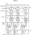
- FIG. 4 is a diagram showing the configuration of the drive signal selection circuit 200.
- the drive signal selection circuit 200 includes a selection control circuit 210 and a plurality of selection circuits 230.
- FIG. 4 shows an example of the head chip 300 to which the drive signal VOUT output from the drive signal selection circuit 200 is supplied.
- the head chip 300 includes p ejecting portions 600 each having the piezoelectric element 60.
- the print data signal cSI, the latch signal cLAT, the change signal cCH, and the clock signal cSCK are input to the selection control circuit 210. Further, the selection control circuit 210 is provided with sets of a shift register (S/R) 212, a latch circuit 214, and a decoder 216 corresponding to the p ejecting portions 600 of the head chip 300, respectively. That is, the drive signal selection circuit 200 includes the same number of sets of the shift register 212, the latch circuit 214, and the decoder 216 as the p ejecting portions 600 of the head chip 300.
- the print data signal cSI is a signal synchronized with the clock signal cSCK, a signal of total of 2p bits that includes a 2-bit print data [SIH, SIL] for selecting one of the large dot LD, the medium dot MD, the small dot SD, and non-recording ND for each of the p ejecting portions 600.
- the print data signal cSI input to the drive signal selection circuit 200 corresponds to the p ejecting portions 600, and is held in the shift register 212 for each of the two bits of print data [SIH, SIL] included in the print data signal cSI.
- the p-stage shift registers 212 corresponding to the p ejecting portions 600 are coupled in cascade to each other, and the print data [SIH, SIL] serially input as the print data signal cSI is sequentially transferred to the subsequent stage with the clock signal cSCK.
- the shift register 212 into which the print data signal cSI is input is described as 1st stage, 2nd stage,...., p-th stage in order from upstream to downstream.
- Each of the p latch circuits 214 latches the 2-bit print data [SIH, SIL] held in each of the p shift registers 212 at the rise of the latch signal cLAT.
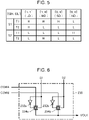
- FIG. 5 is a diagram showing the decoding contents in the decoder 216.
- the decoder 216 outputs selection signals S1 and S2 according to the latched 2-bit print data [SIH, SIL]. For example, when the 2-bit print data [SIH, SIL] is [1,0], the decoder 216 outputs logic levels of the selection signal S1 to the selection circuit 230 as H and L levels in the periods T1 and T2, and outputs logic levels of the selection signal S2 to the selection circuit 230 as L and H levels in the periods T1 and T2.
- the selection circuit 230 is provided corresponding to each of the ejecting portions 600. That is, the number of selection circuits 230 included in the drive signal selection circuit 200 is p, which is the same as the number of ejecting portions 600 included in the corresponding head chip 300.
- FIG. 6 is a diagram showing a configuration of the selection circuit 230 corresponding to one ejecting portion 600. As shown in FIG. 6 , the selection circuit 230 has inverters 232a and 232b, which are NOT circuits, and transfer gates 234a and 234b.
- the selection signal S1 is input to a positive control terminal of the transfer gate 234a to which a circle is not attached, and meanwhile, is also logically inverted by the inverter 232a and input to a negative control terminal of the transfer gate 234a to which a circle is attached. Further, the drive signal COMA is supplied to an input terminal of the transfer gate 234a.
- the selection signal S2 is input to a positive control terminal of the transfer gate 234b to which a circle is not attached, and meanwhile, is also logically inverted by the inverter 232b and input to a negative control terminal of the transfer gate 234b to which a circle is attached. Further, the drive signal COMB is supplied to the input terminal of the transfer gate 234b. Then, the output terminals of the transfer gates 234a and 234b are commonly coupled, and the drive signal VOUT is output from the output terminals.
- the transfer gate 234a makes conduction between the input terminal and the output terminal when the selection signal S1 is the H level, and does not make conduction between the input terminal and the output terminal when the selection signal S1 is the L level.
- the transfer gate 234b makes conduction between the input terminal and the output terminal when the selection signal S2 is the H level, and does not make conduction between the input terminal and the output terminal when the selection signal S2 is the L level. That is, the selection circuit 230 selects the waveforms of the drive signals COMA and COMB based on the input selection signals S1 and S2, and outputs the drive signal VOUT of the selected waveform.
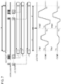
- FIG. 7 is a diagram for describing the operation of the drive signal selection circuit 200.
- the print data [SIH, SIL] included in the print data signal cSI is serially input in synchronization with the clock signal cSCK, and is sequentially transferred in the shift register 212 corresponding to the ejecting portion 600. Then, when the input of the clock signal cSCK is stopped, the 2-bit print data [SIH, SIL] corresponding to each of the p ejecting portions 600 is held in each shift register 212.
- the print data [SIH, SIL] included in the print data signal cSI is input to the ejecting portions 600 of the p-th stage, ..., 2nd stage, and 1st stage shift register 212 in the corresponding order.
- each of the latch circuits 214 latches the 2-bit print data [SIH, SIL] held in the shift registers 212 all at once.
- LT1, LT2, ..., LTp indicates 2-bit print data [SIH, SIL] latched by the latch circuits 214 corresponding to the 1st stage, 2nd stage, ..., p-th stage shift registers 212.
- the decoder 216 outputs the logic levels of the selection signals S1 and S2 as shown in FIG. 5 in each of the periods T1 and T2 according to the dot size defined by the latched 2-bit print data [SIH, SIL].
- the decoder 216 sets the selection signal S1 to the H and H levels in the period T1 and T2, and sets the selection signal S2 to the L and L levels in the periods T1 and T2.
- the selection circuit 230 selects the trapezoidal waveform Adp1 in the period T1 and selects the trapezoidal waveform Adp2 in the period T2.
- the drive signal VOUT corresponding to the large dot LD shown in FIG. 3 is generated.
- the decoder 216 sets the selection signal S1 to the H and L levels in the period T1 and T2, and sets the selection signal S2 to the L and H levels in the periods T1 and T2.
- the selection circuit 230 selects the trapezoidal waveform Adp1 in the period T1 and selects the trapezoidal waveform Bdp2 in the period T2.
- the drive signal VOUT corresponding to the medium dot MD shown in FIG. 3 is generated.
- the decoder 216 sets the selection signal S1 to the H and L levels in the period T1 and T2, and sets the selection signal S2 to the L and L levels in the periods T1 and T2.
- the selection circuit 230 selects the trapezoidal waveform Adp1 in the period T1 and does not select either the trapezoidal waveform Adp2 or Bdp2 in the period T2.
- the drive signal VOUT corresponding to the small dot SD shown in FIG. 3 is generated.
- the decoder 216 sets the selection signal S1 to the L and L levels in the period T1 and T2, and sets the selection signal S2 to the H and L levels in the periods T1 and T2.
- the selection circuit 230 selects the trapezoidal waveform Bdp1 in the period T1 and does not select either the trapezoidal waveform Adp2 or Bdp2 in the period T2.
- the drive signal VOUT corresponding to the non-recording ND shown in FIG. 3 is generated.
- the drive signal selection circuit 200 selects the waveforms of the drive signals COMA and COMB based on the print data signal cSI, the latch signal cLAT, the change signal cCH, and the clock signal cSCK, and outputs the selected waveforms as the drive signal VOUT. Then, the drive signal selection circuit 200 selects or does not select the waveforms of the drive signals COMA and COMB, so that the size of the dots formed on the medium is controlled, and as a result, dots of a desired size are formed on the medium in the liquid ejecting apparatus 1.
- At least one of the print data signal SI, which is a digital signal input to the ejecting heads 100 corresponding to the print data signal cSI, the latch signal LAT, which is a digital signal input to the ejecting heads 100 corresponding to the latch signal cLAT, and the change signal CH, which is a digital signal input to the ejecting heads 100 corresponding to the change signal cCH, is an example of a signal that defines the ink ejection timing. That is, the digital signal output by the head control circuit 21 and input to the diagnostic circuit 250 includes a signal defining the ink ejection timing and the clock signal SCK.
- FIG. 8 is a diagram showing a schematic structure of the liquid ejecting apparatus 1.
- the head unit 20 has six ejecting heads 100.
- the six ejecting heads 100 may be referred to as ejecting heads 100-1 to 100-6.
- a Y direction corresponding to a transport direction in which a medium P is transported
- an X direction orthogonal to the Y direction and parallel to a horizontal plane and corresponding to a main scanning direction
- a Z direction that is an up-and-down direction of the liquid ejecting apparatus 1 and corresponds to the vertical direction when the liquid ejecting apparatus 1 is installed.
- the tip side of an arrow indicating the X direction shown may be referred to as a +X side, and the starting point side is referred to as a -X side
- the tip side of an arrow indicating the Y direction shown may be referred to as a +Y side
- the starting point side is referred to as a - Y side
- the tip side of an arrow indicating the Z direction shown may be referred to as a +Z side
- the starting point side may be referred to as a -Z side.
- it is assumed that the X direction, the Y direction, and the Z direction are orthogonal to each other, but the present disclosure is not limited to the case where configurations of the liquid ejecting apparatus 1 are arranged orthogonally to each other.
- the liquid ejecting apparatus 1 includes, in addition to the control unit 10 and the head unit 20 described above, a transport unit 40 for transporting the medium P, and a liquid container 5 for storing ink.
- control unit 10 includes the main control circuit 11 and the power supply circuit 12, and controls the operation of the liquid ejecting apparatus 1 including the head unit 20. Further, the control unit 10 may include, in addition to the main control circuit 11 and the power supply circuit 12, a storage circuit for storing various information for the liquid ejecting apparatus 1, an interface circuit for communicating with a host computer or the like provided outside the liquid ejecting apparatus 1, or the like.
- the control unit 10 receives an image signal input from an external device such as the host computer provided outside the liquid ejecting apparatus 1, and generates a medium transport signal PT as a transport control signal for controlling the transport of the medium P based on the received image signal and outputs the medium transport signal PT to the transport unit 40.
- the transport unit 40 transports the medium P along the Y direction.
- a transport unit 40 includes a roller (not shown) for transporting the medium P, a motor for rotating the roller, and the like.
- the liquid container 5 stores ink to be ejected to the medium P.
- the liquid container 5 includes four containers for individually storing four color inks of cyan C, magenta M, yellow Y, and black K.
- the ink stored in the liquid container 5 is supplied to the ejecting heads 100 of the head unit 20 via a tube (not shown) or the like.
- the liquid container 5 that supplies ink to the ejecting heads 100 is an example of a liquid accommodating container.
- the number of containers included in the liquid container 5 is not limited to four.
- the liquid container 5 may be provided with a container in which inks of different colors are stored in place of or in addition to inks of colors other than cyan C, magenta M, yellow Y, and black K, and a plurality of containers of any one of cyan C, magenta M, yellow Y, and black K may be provided.
- the head unit 20 includes ejecting heads 100-1 to 100-6 arranged side by side in the X direction.
- the ejecting heads 100-1 to 100-6 included in the head unit 20 are arranged side by side from the -X side to the +X side in the order of the ejecting head 100-1, the ejecting head 100-2, ejecting head 100-3, ejecting head 100-4, ejecting head 100-5, and ejecting head 100-6 so as to be equal to or larger than the width of the medium P in the X direction.
- the head unit 20 distributes the ink supplied from the liquid container 5 to each of the ejecting heads 100-1 to 100-6, and operates based on the image information signal IP input from the control unit 10 to eject the ink supplied from the liquid container 5 from each of the ejecting heads 100-1 to 100-6 to a desired position on the medium P.
- the number of ejecting heads 100 included in the head unit 20 is not limited to six, and may be five or less, or seven or more.
- the control unit 10 generates the image information signal IP based on the image signal input from the host computer or the like, and uses the generated image information signal IP to control the operation of the head unit 20 and to control the transport of the medium P in the transport unit 40.
- the ink ejected by each of the ejecting heads 100-1 to 100-6 can be landed at a desired position on the medium P.
- a desired image is formed on the medium P.
- FIG. 9 is an exploded perspective view of the head unit 20 when viewed from the -Z side.
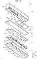
- FIG. 10 is an exploded perspective view of the head unit 20 when viewed from the +Z side.
- the head unit 20 includes an introduction flow path portion G1 for introducing the ink supplied from the liquid container 5 into the head unit 20, a supply flow path portion G2 for supplying the introduced ink to the ejecting head 100, a liquid ejecting portion G3 having a plurality of ejecting heads 100 for ejecting ink, an ejection control portion G4 for controlling the ejection of ink from the ejecting head 100, and an accommodating portion G5 for accommodating the introduction flow path portion G1, the supply flow path portion G2, the liquid ejecting portion G3, and the ejection control portion G4.
- the introduction flow path portion G1, the supply flow path portion G2, the liquid ejecting portion G3, and the ejection control portion G4 are directed from the -Z side to the +Z side in the Z direction, and the ejection control portion G4, the introduction flow path portion G1, the supply flow path portion G2, and the liquid ejecting portion G3 are stacked in this order.
- the accommodating portion G5 is provided so as to accommodate the ejection control portion G4, the introduction flow path portion G1, the supply flow path portion G2, and the liquid ejecting portion G3, which are stacked.
- the introduction flow path portion G1, the supply flow path portion G2, the liquid ejecting portion G3, the ejection control portion G4, and the accommodating portion G5 are fixed to each other by fixing means such as an adhesive or a screw (not shown).
- the introduction flow path portion G1 includes a plurality of inlets SI1 according to the number of types of ink supplied to the head unit 20, and a plurality of outlets DI1 according to the number of types of ink and according to the number of ejecting heads 100 included in the head unit 20.
- the plurality of inlets SI1 are positioned side by side along the side of the introduction flow path portion G1 on -Y side on a surface of the introduction flow path portion G1 on the -Z side. Then, a tube (not shown) or the like to which ink is supplied from the liquid container 5 shown in FIG. 8 is coupled to each of the inlets SI1.
- the plurality of outlets DI1 are positioned on a surface of the introduction flow path portion G1 on the +Z side. Inside the introduction flow path portion G1, ink flow paths are formed through which the inlets SI1 and the outlets DI1 corresponding to the inlets SI1 communicate with each other.
- the supply flow path portion G2 has a plurality of liquid supply units U2 according to the number of ejecting heads 100 included in the head unit 20. Further, each of the plurality of liquid supply units U2 has a plurality of inlets SI2 according to the number of types of ink supplied to the head unit 20, and a plurality of outlets DI2 according to the number of types of ink supplied to the head unit 20.
- the plurality of inlets SI2 are positioned on the -Z side of the liquid supply unit U2 and are coupled to the outlets DI1 included in the introduction flow path portion G1. That is, the supply flow path portion G2 has inlets SI2 corresponding to the outlets DI1 of the introduction flow path portion G1, respectively. Further, the outlets DI2 are positioned on the -Z side of the liquid supply unit U2. Inside the liquid supply unit U2, an ink flow path is formed through which the inlets SI2 and the outlets DI2 corresponding to the inlets SI2 communicate with each other.
- the liquid ejecting portion G3 has the ejecting heads 100-1 to 100-6 and a support member 35.
- Each of the ejecting heads 100-1 to 100-6 is positioned on the +Z side of the support member 35, and is fixed to the support member 35 by a fixing means such as an adhesive or a screw (not shown).
- a plurality of inlets SI3 are positioned on the -Z side of each of the ejecting heads 100-1 to 100-6.
- the plurality of inlets SI3 of each of the ejecting heads 100-1 to 100-6 pass through the openings formed in the support member 35 and are exposed to the -Z side of the liquid ejecting portion G3.
- the plurality of inlets SI3 are coupled to the plurality of outlets DI2 included in the supply flow path portion G2. That is, the liquid ejecting portion G3 has the inlets SI3 corresponding to the outlets DI2 of the supply flow path portion G2, respectively.
- the ink stored in the liquid container 5 is introduced from the inlets SI1 of the introduction flow path portion G1 via a tube (not shown) or the like.
- the ink introduced from the inlets SI1 is distributed corresponding to the plurality of ejecting heads 100 by the ink flow path (not shown) provided inside the introduction flow path portion G1, and then is supplied to the liquid supply unit U2 via the outlets DI1 and the inlets SI2.
- ink supplied to the liquid supply unit U2 is supplied to the plurality of ejecting heads 100 included in the liquid ejecting portion G3 via the ink flow path, the outlets DI2, and the inlets SI3 provided inside the liquid supply unit U2. That is, in the present embodiment, the introduction flow path portion G1 and the liquid supply unit U2 function as a distribution flow path member for distributing and supplying the ink supplied from the outlets DI1 to the head unit 20 to each of the ejecting heads 100-1 to 100-6.
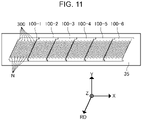
- FIG. 11 is a view when the head unit 20 is viewed from the +Z side.
- each of the ejecting heads 100-1 to 100-6 has six head chips 300 arranged side by side in the X direction.
- each head chip 300 has a plurality of nozzles N for ejecting the supplied ink to the medium P.
- the plurality of nozzles N included in each of the head chips 300 are arranged side by side in a column direction RD in a plane perpendicular to the Z direction and formed by the X direction and the Y direction.
- a plurality of nozzles N arranged side by side in the column direction RD may be referred to as a nozzle row.
- the number of head chips 300 included in each of the ejecting heads 100-1 to 100-6 is not limited to six.
- FIG. 12 is an exploded perspective view showing a schematic configuration of the ejecting head 100.
- the ejecting head 100 includes a filter portion 110, a sealing member 120, a wiring substrate 130, a holder 140, six head chips 300, and a fixing plate 150.
- the ejecting head 100 is configured with the filter portion 110, the sealing member 120, the wiring substrate 130, the holder 140, and the fixing plate 150 being superimposed in this order from the -Z side to the +Z side in the Z direction, and six head chips 300 are accommodated between the holder 140 and the fixing plate 150.
- the filter portion 110 has a substantially parallelogram shape in which two opposite sides extend in the X direction and the other two opposite sides extend in the column direction RD.
- the filter portion 110 has four filters 113 and four inlets SI3.
- the four inlets SI3 are positioned on the -Z side of the filter portion 110, and are provided corresponding to the four filters 113 positioned inside the filter portion 110.
- the filter 113 collects air bubbles and foreign substances contained in the ink introduced from the inlet SI3. Then, ink is supplied to the inlets SI3 from the liquid container 5.
- the inlets SI3 are an example of supply ports.
- the sealing member 120 is positioned on the +Z side of the filter portion 110, and has a substantially parallelogram shape in which two opposite sides extend in the X direction and the other two opposite sides extend in the column direction RD. Through openings 125 through which liquid flow paths 145 to be described later is inserted, are provided at four corners of the sealing member 120.
- the sealing member 120 is formed of, for example, an elastic member such as rubber.
- the wiring substrate 130 is positioned on the +Z side of the sealing member 120, and has a substantially parallelogram shape in which two opposite sides extend in the X direction and the other two opposite sides extend in the column direction RD. Further, cutout portions 135 through which the liquid flow paths 145 to be described later passes are formed at the four corners of the wiring substrate 130.
- the wiring substrate 130 is formed with wiring for propagating, to the head chips 300, various signals such as the drive signals COMA and COMB and the voltages VHV and VDD supplied to the ejecting head 100, and is provided with the above-mentioned diagnostic circuit 250. That is, the wiring substrate 130 is positioned toward the +Z side further than the inlets SI3. In other words, the inlets SI3 are positioned above the wiring substrate 130 in the vertical direction. A specific example of the configuration of the wiring substrate 130 will be described later.
- the holder 140 is positioned on the +Z side of the wiring substrate 130, and has a substantially parallelogram shape in which two opposite sides extend in the X direction and the other two opposite sides extend in the column direction RD.
- the holder 140 has holder members 141, 142, and 143.
- the holder members 141, 142, and 143 are stacked in the order of the holder member 141, the holder member 142, and the holder member 143 from the -Z side to the +Z side in the Z direction. Further, the holder member 141 and the holder member 142 are adhered to each other by adhesive or the like therebetween, and the holder member 142 and the holder member 143 are adhered to each other by an adhesive or the like therebetween.
- an accommodation space having an opening (not shown) on the +Z side is formed inside the holder member 143.
- the head chips 300 are accommodated in the accommodation space formed inside the holder member 143.
- the accommodation space formed inside the holder member 143 may be a plurality of spaces that can individually accommodate the six head chips 300, respectively, and may be one space that can accommodate the six head chips 300 in common.
- the holder 140 is provided with slit holes 146 corresponding to the six head chips 300, respectively.
- Flexible wiring substrates 346 for propagating various signals such as drive signals COMA and COMB, the voltages VHV and VDD to the head chips 300 is inserted into the slit holes 146. Then, the six head chips 300 accommodated in the accommodation space formed inside the holder member 143 are fixed to the holder 140 by an adhesive or the like.
- liquid flow paths 145 are provided at the four corners of the surface of the holder 140 on the -Z side.
- the liquid flow paths 145 is coupled to the filter portion 110 through the respective through openings 125 provided in the sealing member 120.
- the ink supplied from the inlets SI3 is supplied to the holder 140 via the liquid flow paths 145.
- the ink supplied to the holder 140 is distributed inside the holder 140 corresponding to the six head chips 300, and then supplied to each of the six head chips 300.
- the fixing plate 150 is positioned on the +Z side of the holder 140 and seals the accommodation space in which the six head chips 300 formed inside the holder member 143 are accommodated.
- the fixing plate 150 has a flat surface portion 151 and bent portions 152, 153, and 154.
- the flat surface portion 151 has a substantially parallelogram shape in which two opposite sides extend in the X direction and the other two opposite sides extend in the column direction RD.
- the flat surface portion 151 is formed with six openings 155 for exposing the head chips 300. Then, the head chips 300 are fixed to the fixing plate 150 so that two rows of nozzle rows are exposed to the flat surface portion 151 via the openings 155.
- the bent portion 152 is a member coupled to one side extending along the X direction of the flat surface portion 151 and integrated with the flat surface portion 151 bent toward the -Z side
- the bent portion 153 is a member coupled to one side extending along the column direction RD of the flat surface portion 151 and integrated with the flat surface portion 151 bent toward the -Z side
- the bent portion 154 is a member coupled to the other side extending along the column direction RD of the flat surface portion 151 and integrated with the flat surface portion 151 bent toward the -Z side.
- the head chips 300 are positioned on the +Z side of the holder 140 and on the -Z side of the fixing plate 150. Then, the head chips 300 are accommodated in the accommodation space formed by the holder member 143 of the holder 140 and the fixing plate 150, and is fixed to the holder member 143 and the fixing plate 150.
- FIG. 13 is a cross-sectional view showing a schematic structure of the head chip 300.
- the cross-sectional view of the head chip 300 shown in FIG. 13 shows a case where the head chip 300 is cut in a direction perpendicular to the column direction RD to include at least one nozzle N. As shown in FIG.
- the head chip 300 has a nozzle plate 310 provided with a plurality of nozzles N for ejecting ink, a flow path forming substrate 321 that defines a communication flow path 355, an individual flow path 353, and a reservoir R, a pressure chamber substrate 322 that defines a pressure chamber C, a protection substrate 323, a compliance portion 330, a diaphragm 340, the piezoelectric element 60, the flexible wiring substrate 346, and a case 324 that defines the reservoir R and a liquid inlet 351. Then, ink is supplied to the head chips 300 from a liquid outlet (not shown) provided in the holder 140 via the liquid inlet 351.
- a liquid outlet not shown
- the ink supplied to the head chip 300 reaches the nozzle N via the ink flow path 350 including the reservoir R, the individual flow path 353, the pressure chamber C, and the communication flow path 355. Then, the ink reached by the nozzles N is ejected as the piezoelectric element 60 is driven.
- the ink flow path 350 is formed by stacking the flow path forming substrate 321, the pressure chamber substrate 322, and the case 324 in the Z direction.
- the ink introduced into the case 324 from the liquid inlet 351 is stored in the reservoir R.
- the reservoir R is a common flow path communicating with a plurality of individual flow paths 353 corresponding to the plurality of nozzles N constituting the nozzle row, respectively.
- the ink stored in the reservoir R is supplied to the pressure chamber C via the individual flow path 353.
- the pressure chamber C applies pressure to the stored ink to eject the ink supplied to the pressure chamber C from the nozzle N via the communication flow path 355.
- the diaphragm 340 is positioned on the -Z side of the pressure chamber C to seal the pressure chamber C, and the piezoelectric element 60 is positioned on the -Z side of the diaphragm 340.
- the piezoelectric element 60 is composed of a piezoelectric body and a pair of electrodes formed on both sides of the piezoelectric body.
- the drive signal VOUT is supplied to one of the pair of electrodes of the piezoelectric element 60 via the flexible wiring substrate 346, and the reference voltage signal VBS is supplied to the other of the pair of electrodes of the piezoelectric element 60 via the flexible wiring substrate 346. Then, the piezoelectric body is displaced according to the potential difference generated between the pair of electrodes. That is, the piezoelectric element 60 including the piezoelectric body is driven. Then, as the piezoelectric element 60 is driven, the diaphragm 340 provided with the piezoelectric element 60 is deformed, so that the internal pressure of the pressure chamber C changes, and as a result, the ink stored in the pressure chamber C is ejected from the nozzle N via the communication flow path 355.
- the nozzle plate 310 and the compliance portion 330 are fixed to the +Z side of the flow path forming substrate 321.
- the nozzle plate 310 is positioned on the +Z side of the communication flow path 355.
- a plurality of nozzles N are arranged side by side on the nozzle plate 310 in the column direction RD. That is, the nozzle plate 310 has the plurality of nozzles N for ejecting ink.
- the compliance portion 330 is positioned on the +Z side of the reservoir R and the individual flow path 353, and includes a sealing film 331 and a support 332.
- the sealing film 331 is a flexible film-like member, and seals the reservoir R and the individual flow path 353 on the +Z side.
- the compliance portion 330 configured as described above protects the head chip 300 and reduces ink pressure fluctuations inside the reservoir R and inside the individual flow path 253.
- the configuration including the piezoelectric element 60, the diaphragm 340, the nozzle N, the individual flow path 353, the pressure chamber C, and the communication flow path 355 corresponds to the ejecting portion 600 described above.
- the head chip 300 including the nozzle plate 310 is an example of an ejecting module.
- the ejecting head 100 distributes the ink supplied from the liquid container 5 to the plurality of nozzles N, and ejects the ink from the nozzles N by driving the piezoelectric element 60 generated based on the drive signal VOUT and the reference voltage signal VBS supplied via the flexible wiring substrate 346.
- the drive signal selection circuit 200 that outputs the drive signal VOUT may be provided on the wiring substrate 130, or may be provided on the flexible wiring substrate 346 corresponding to each of the head chips 300.
- COF Chip On Film
- the ejection control portion G4 is positioned on the -Z side of the introduction flow path portion G1 and includes a wiring substrate 410 and a wiring substrate 420.
- the wiring substrate 410 includes a surface 411 and a surface 412 positioned on the opposite side of the surface 411. Then, the wiring substrate 410 is disposed such that the surface 412 faces the introduction flow path portion G1, the supply flow path portion G2, and the liquid ejecting portion G3, and the surface 411 faces the side opposite to the introduction flow path portion G1, the supply flow path portion G2, and the liquid ejecting portion G3.
- the drive signal output circuit 50 for outputting the drive signals COMA and COMB is provided on the surface 411 of the wiring substrate 410. Further, a coupling portion 413 is provided on the surface 412 of the wiring substrate 410. The coupling portion 413 electrically couples the wiring substrate 410 to the wiring substrate 420, propagates the drive signals COMA and COMB generated by the drive signal output circuit 50, and propagates a plurality of signals including basic drive signals dA and dB that are the basis of the drive signals COMA and COMB output by the drive signal output circuit 50.
- the wiring substrate 420 includes a surface 421 and a surface 422 positioned on the opposite side of the surface 421. Then, the wiring substrate 420 is disposed so that the surface 422 faces the introduction flow path portion G1, the supply flow path portion G2, and the liquid ejecting portion G3, and the surface 421 faces the side opposite to the introduction flow path portion G1, the supply flow path portion G2, and the liquid ejecting portion G3. Further, a cutout portion 427 for the inlets SI1 of the introduction flow path portion G1 to pass through is formed on the -Y side of the wiring substrate 420.
- a semiconductor device 423 and coupling portions 424, 425, and 426 are provided on the surface 421 of the wiring substrate 420.
- the coupling portion 424 is coupled to the coupling portion 413 provided on the wiring substrate 410.
- the wiring substrate 420 is electrically coupled to the wiring substrate 410.
- a board-to-board (B-to-B) connector that electrically couples the wiring substrate 410 to the wiring substrate 420 without using a cable is used.
- the semiconductor device 423 is a circuit component that constitutes at least a part of the head control circuit 21 described above, and includes, for example, a SoC or the like.
- the semiconductor device 423 is provided in a region of the wiring substrate 420 further to the -X side than the coupling portion 424.
- the voltages VHV and VDD that function as the power supply voltage of the head unit 20 are input to the coupling portion 426.
- the coupling portion 426 is positioned on the -Y side of the semiconductor device 423 and on the -X side of the cutout portion 427.
- the image information signal IP output by the control unit 10 is input to the coupling portion 425. That is, the coupling portion 425 has a plurality of terminals through which the input image information signal IP propagates.
- the coupling portion 425 is disposed on the -Y side of the semiconductor device 423 and on the -X side of the coupling portion 426 so that a plurality of terminals into which the image information signal IP is input are lined up in the X direction.
- the image information signal IP input to the coupling portion 425 is a signal compliant with a communication standard for high-speed communication such as PCIe, as described above. Therefore, it is preferable that the coupling portion 425 and the cable coupled to the coupling portion 425 have a configuration capable of stably propagating signals of several Gbps, and it is preferable that, for the coupling portion 425, for example, a high-speed transmission connector, such as an HDMI (registered trademark) (high-definition multimedia interface) connector compliant with HDMI communication standard and a USB connector compliant with universal serial bus (USB) communication standard, is used.
- HDMI registered trademark
- USB universal serial bus
- the coupling portion 426 since the voltages VHV and VDD are propagated to the coupling portion 426, a cable capable of stably propagating high voltage signals can be coupled to the coupling portion 426, and it is preferable that, for example, an FFC connector to which a flexible cable can be coupled is used.
- the accommodating portion G5 includes a housing 450 in which opening holes 451, 452, and 453 are formed.
- the housing 450 has a substantially rectangular shape including a pair of long sides extending in the X direction and a pair of short sides extending in the Y direction when viewed in the Z direction, and is formed of, for example, a metal such as aluminum, a resin, or the like.
- An opening 454 is formed on the +Z side of the housing 450.
- the opening 454 accommodates the introduction flow path portion G1, the supply flow path portion G2, the liquid ejecting portion G3, and the ejection control portion G4. That is, the opening 454 forms an accommodation space for accommodating the introduction flow path portion G1, the supply flow path portion G2, the liquid ejecting portion G3, and the ejection control portion G4. Then, the introduction flow path portion G1, the supply flow path portion G2, the liquid ejecting portion G3, and the ejection control portion G4 accommodated in the opening 454 are fixed to the housing 450 by fixing means such as an adhesive or a screw (not shown).
- fixing means such as an adhesive or a screw (not shown).
- the opening 454 may be configured to be sealed by the support member 35 of the liquid ejecting portion G3 in a state of accommodating the introduction flow path portion G1, the supply flow path portion G2, and the liquid ejecting portion G3.
- the opening holes 451, 452, and 453 of the housing 450 are arranged side by side in the order of the opening hole 451, the opening hole 452, and the opening hole 453 from the -X side to the +X side in the X direction on the -Y side of the housing 450.
- the coupling portion 425 of the ejection control portion G4 accommodated in the accommodation space is inserted into the opening hole 451.
- the coupling portion 426 of the ejection control portion G4 accommodated in the accommodation space is inserted into the opening hole 452.
- the inlet SI1 of the introduction flow path portion G1 is inserted into the opening hole 453 after passing through the cutout portion 427 of the wiring substrate 420.
- the opening holes 451, 452, and 453 expose, to the outside of the head unit 20, the inlet SI1 for supplying ink to the introduction flow path portion G1, the supply flow path portion G2, and the liquid ejecting portion G3 accommodated in the housing 450, and the coupling portions 425 and 426 for propagating various signals to the liquid ejecting portion G3 and the ejection control portion G4.
- the accommodating portion G5 protects the introduction flow path portion G1, the supply flow path portion G2, the liquid ejecting portion G3, and the ejection control portion G4 with the housing 450, and the coupling portions 425 and 426 for propagating various signals to the inlet SI1 for supplying ink, the liquid ejecting portion G3, and the ejection control portion G4 are exposed to the outside of the head unit 20, and thus the replacement work of the head unit 20 becomes easy, and the maintainability of the liquid ejecting apparatus 1 can be improved.
- the ejecting head 100 in the present embodiment generates the drive signal VOUT by selecting the trapezoidal waveforms Adp1, Adp2, Bdp1, and Bdp2 included in the drive signals COMA and COMB at timing defined by the print data signal cSI corresponding to the print data signal SI, the clock signal cSCK corresponding to the clock signal SCK, the latch signal cLAT corresponding to the latch signal LAT, and the change signal cCH corresponding to the change signal CH. Then, the ejecting head 100 supplies the generated drive signal VOUT to the piezoelectric element 60 included in the ejecting portion 600.
- the piezoelectric element 60 is driven according to the potential of the drive signal VOUT, and an amount of ink corresponding to the drive amount of the piezoelectric element 60 is ejected to the medium P. As a result, an image is formed on the medium P.
- the liquid ejecting apparatus 1 in the present embodiment has the diagnostic circuit 250 for diagnosing the presence or absence of an abnormality in the ejecting head 100.
- the diagnostic circuit 250 diagnoses an operation abnormality in the ejecting head 100 or a temperature abnormality in the ejecting head 100. Further, the diagnostic circuit 250 in the present embodiment also detects whether or not the ink mist entering into the ejecting head 100 adheres to the inside of the ejecting head 100.
- an example of the ink mist entering into the ejecting head 100 includes ink mist floating inside the liquid ejecting apparatus 1 due to a part of the ink ejected from the nozzles N becoming mist before landing on the medium P, and ink mist floating inside the liquid ejecting apparatus 1 by the ink ejected from the nozzles N becoming mist by being re-floated by the air flow generated by the transport of the medium P after landing on the medium P.
- the ink mist floating inside the liquid ejecting apparatus 1 is extremely small, and thus it is charged by the Lenard effect. For this reason, the ink mist is attracted to conductive portions such as wiring patterns and terminals that propagate various signals to the ejecting head 100, and enters into the ejecting head 100.
- the diagnostic circuit 250 detects the presence or absence of an operation abnormality or temperature abnormality occurring in the ejecting head 100, and also detects whether or not ink adheres to the inside of the ejecting head 100, thereby reducing the possibility that an abnormality occurs due to the ink adhering to the inside of the ejecting head 100.
- FIG. 14 is a diagram showing an example of a configuration of the wiring substrate 130 when the wiring substrate 130 having an integrated circuit 550 including the diagnostic circuit 250 is viewed from the -Z side.
- FIG. 15 is a diagram showing an example of the configuration of the wiring substrate 130 when the wiring substrate 130 is viewed from the +Z side.
- FIG. 14 shows a part of the configuration that cannot be visually recognized when the wiring substrate 130 is viewed from the -Z side by a broken line
- FIG. 15 shows a part of the configuration that cannot be visually recognized when the wiring substrate 130 is viewed from the +Z side by a broken line.
- the configuration of the wiring substrate 130 provided with the integrated circuit 550 including the diagnostic circuit 250 will be described.
- the wiring substrate 130 includes a substrate 500, coupling portions 520 and 530, and the integrated circuit 550.
- the wiring substrate 130 may include various electronic components such as a resistance element, a capacitance element, an induction element, and a semiconductor element in addition to the substrate 500, coupling portions 520 and 530, and the integrated circuit 550. Further, although not shown, the wiring substrate 130 may include the temperature detection circuit 260 described above.
- the substrate 500 has a substantially parallelogram shape having sides 511 and 512 positioned opposite to each other and sides 513 and 514 positioned opposite to each other, and has a surface 501 and a surface 502 different from the surface 501 and positioned opposite to the surface 501.
- the surface 501 is an example of a first surface
- the surface 502 is an example of a second surface.
- the side 511 extends in the X direction
- the side 512 is positioned on the -Y side of the side 511 and extends in the X direction
- the side 513 extends in the column direction RD
- the side 514 is positioned on the -X side of the side 513 and extends in the column direction RD
- the surface 501 is provided on the -Z side
- the surface 502 is provided on the +Z side.
- the substrate 500 in the substrate 500, the side 511 and the side 512 are positioned opposite to each other in the direction along the Y direction, the side 513 and the side 514 are positioned opposite to each other in the direction along the X direction, the surface 501 is positioned to face upward and the surface 502 is positioned to face downward in the vertical direction.
- the substrate 500 is preferably positioned so that the surface 501 is orthogonal to the vertical direction.
- cutout portions 135 are formed at the four corners of the substrate 500.
- the liquid flow paths 145 provided in the holder 140 pass through the cutout portions 135.
- the ejecting head 100 has the liquid flow paths 145 that communicate with the inlets SI3, and at least some of the liquid flow paths 145 pass through the cutout portions 135 that penetrates the surface 501 and the surface 502 of the substrate 500.
- the cutout portions 135 may be configured such that the liquid flow paths 145 provided in the holder 140 positioned on the +Z side of the substrate 500 and the inlets SI3 included in the filter portion 110 positioned on the -Z side of the substrate 500 can be communicatively coupled to each other, and are not limited to being cut out. That is, the substrate 500 may have holes provided to penetrate the surface 501 and the surface 502 for inserting the liquid flow paths 145.
- the cutout portions 135 through which the liquid flow paths 145 pass are an example of a penetrating portion.
- the substrate 500 four flat printed circuit (FPC) insertion holes 136 penetrating the surface 501 and the surface 502 of the substrate 500 are formed, and two FPC cutout portions 137 in which a part of each of the side 513 and the side 514 of the substrate 500 is cut out are formed.
- the flexible wiring substrate 346 of each of the six head chips 300 accommodated in the holder 140 passes through each of the four FPC insertion holes 136 and the FPC cutout portions 137.
- the flexible wiring substrate 346 passing through each of the four FPC insertion holes 136 and the FPC cutout portions 137 is electrically coupled to coupling terminals 138 formed on the surface 501 of the substrate 500. In this way, the wiring substrate 130 and the head chip 300 are electrically coupled to each other.
- the substrate 500 will be described as having the surface 501 and the surface 502 positioned opposite to the surface 501 in configuration, but the substrate 500 may be a so-called multilayer substrate including a plurality of wiring layers between the surface 501 and the surface 502.
- the coupling portion 520 has a plurality of terminals 521. Then, the coupling portion 520 is provided on the surface 501 of the substrate 500 so that the plurality of terminals 521 are arranged side by side along the side 511. A flexible cable (not shown) for electrically coupling the wiring substrate 420 to the wiring substrate 130, or the like, is attached to the coupling portion 520 configured in this way. Further, the coupling portion 530 has a plurality of terminals 531. Then, the coupling portion 530 is provided on the surface 501 of the substrate 500 so that the plurality of terminals 531 are arranged side by side along the side 512. A flexible cable (not shown) for electrically coupling the wiring substrate 420 to the wiring substrate 130 is attached to the coupling portion 530 configured in this way.
- the coupling portions 520 and 530 electrically couple the wiring substrate 420 to the wiring substrate 130 via a flexible cable (not shown).
- the six print data signals SI corresponding to the head chips 300-1 to 300-6 output by the wiring substrate 420, the clock signal SCK, the latch signal LAT, the change signal CH, and the drive signals COMA and COMB are input.
- At least one of the coupling portions 520 and 530 is an example of a connector. Then, various signals are input to the wiring substrate 130 from the wiring substrate 420 via the coupling portions 520 and 530, and various signals output by the ejecting head 100 including the wiring substrate 130 are output to the wiring substrate 420.
- the integrated circuit 550 is a substantially rectangular semiconductor device having sides 551 and 552 positioned opposite to each other and sides 553 and 554 positioned opposite to each other, and includes the diagnostic circuit 250. Then, the integrated circuit 550 is provided on the surface 502 of the substrate 500 so that the side 551 extends along the side 511 in the X direction, the side 552 extends in the X direction on the -Y side of the side 551, the side 553 extends in the Y direction, and the side 554 extends in the Y direction on the -X side of the side 553.
- the integrated circuit 550 is a surface mount component and is preferably electrically coupled to the substrate 500 via a bump electrode.
- the integrated circuit 550 is a surface mount component, and may be, for example, a quad flat no leaded package (QFN) that is electrically coupled to the substrate 500 via a plurality of electrodes formed along the sides 551, 552, 553, and 554, or may be a quad flat package (QFP) that is electrically coupled to the substrate 500 via a plurality of terminals instead of the plurality of electrodes of the QFN; however, as described above, by electrically coupling the integrated circuit 550 to the substrate 500 via the bump electrodes, the bump electrodes to be electrically coupled to the substrate 500 can be provided at a high density in the integrated circuit 550, which makes it possible to miniaturize the integrated circuit 550.
- QFN quad flat no leaded package
- QFP quad flat package
- the integrated circuit 550 is positioned in the vicinity of the coupling portion 520 extending along the side 511. Therefore, the six print data signal SI, the latch signal LAT, the change signal CH, and the clock signal SCK input to the integrated circuit 550 are preferably input from the coupling portion 520, and further, are preferably input from the terminal 521 on the -X side disposed in the vicinity of the integrated circuit 550, among the plurality of terminals 521 provided side by side along the side 511 in the coupling portion 520.
- a plurality of signals including the six print data signals SI corresponding to the six head chips 300, the latch signal LAT, the change signal CH, the clock signal SCK, the drive signals COMA and COMB, the reference voltage signal VBS, and the voltages VHV and VDD are input to the wiring substrate 130 via the coupling portions 520 and 530.
- the six print data signals SI, the latch signal LAT, the change signal CH, and the clock signal SCK are input to the integrated circuit 550.
- the diagnostic circuit 250 included in the integrated circuit 550 diagnoses the presence or absence of an operation abnormality in the ejecting head 100 based on the logic levels of the input six print data signals SI, the latch signal LAT, the change signal CH, and the clock signal SCK.
- the integrated circuit 550 includes the diagnostic circuit 250, and the six print data signals SI, the latch signal LAT, the change signal CH, and the clock signal SCK are input to the diagnostic circuit 250 included in the integrated circuit 550 via the coupling portions 520 and 530. Then, the diagnostic circuit 250 included in the integrated circuit 550 diagnoses the presence or absence of an abnormality in the ejecting head 100 and outputs the abnormality detection signal AD.
- the integrated circuit 550 When it is diagnosed in the diagnostic circuit 250 that no operation abnormality occurs in the ejecting head 100, the integrated circuit 550 generates the six print data signal cSI corresponding, respectively, to the six print data signals SI, the latch signal cLAT corresponding to the latch signal LAT, the change signal cCH corresponding to the change signal CH, and the clock signal cSCK corresponding to the clock signal SCK, and supplies the generated signals to the corresponding coupling terminals 138.
- the drive signals COMA and COMB, the reference voltage signal VBS, and the voltages VHV and VDD are propagated by a wiring pattern (not shown) provided on the substrate 500, and supplied to the corresponding coupling terminals 138.
- the drive signal selection circuit 200 generates the drive signal VOUT based on the input print data signals cSI, the latch signal cLAT, the change signal cCH, the clock signal cSCK, the drive signals COMA and COMB, the reference voltage signal VBS, and the voltages VHV and VDD and outputs the generated drive signal VOUT to the head chips 300. In this way, a predetermined amount of ink is ejected from the nozzles N of the head chips 300 at a predetermined timing.
- the integrated circuit 550 including the diagnostic circuit 250 is provided on the surface 502 of the substrate 500, and the coupling portions 520 and 530 are provided on the surface 501 of the substrate 500. That is, in the wiring substrate 130, the coupling portions 520 and 530, and the integrated circuit 550 are provided on different mounting surfaces of the substrate 500. Then, the substrate 500 is provided on the ejecting head 100 so that the integrated circuit 550 lies on the side closer to the head chips 300. That is, the integrated circuit 550 is positioned between the substrate 500 and the head chips 300.
- the integrated circuit 550 including the diagnostic circuit 250 when the integrated circuit 550 including the diagnostic circuit 250 is disposed in the vicinity of the coupling portion 520 or the coupling portion 530 to which each of the six print data signals SI, the latch signal LAT, the change signal CH, and the clock signal SCK is input, the length of wiring through which each of the six print data signals SI, the latch signal LAT, the change signal CH, and the clock signal SCK is propagated can be shortened. In this way, the possibility that noise is superimposed on the six print data signals SI, the latch signal LAT, the change signal CH, and the clock signal SCK is reduced.
- the integrated circuit 550 by disposing the integrated circuit 550 in the vicinity of the coupling portion 520 or the coupling portion 530, it is possible to improve the accuracy of detecting the presence or absence of an operation abnormality in the ejecting head 100 by the diagnostic circuit 250 of the integrated circuit 550.
- the coupling portions 520 and 530 and the integrated circuit 550 are provided on different mounting surfaces of the substrate 500, and accordingly, the substrate 500 functions as a shielding wall that reduces the possibility that ink mist adheres to the integrated circuit 550, and as a result, even when the integrated circuit 550 is disposed in the vicinity of the coupling portion 520 or the coupling portion 530, the possibility that ink mist unintentionally adheres to the integrated circuit 550 can be reduced. Therefore, the accuracy of detecting the presence or absence of the operation abnormality of the ejecting head 100 by the diagnostic circuit 250 can be improved, and the possibility that malfunction of the integrated circuit 550 occurs due to the influence of the ink mist can be reduced.
- the inlets SI3 for supplying ink to the ejecting head 100 are positioned on the -Z side of the wiring substrate 130. That is, the inlets SI3 are positioned above the substrate 500 in the vertical direction. Therefore, the substrate 500 is positioned between the inlets SI3 supplying ink to the ejecting head 100 and the integrated circuit 550, and as a result, even if ink leaks from the inlets SI3 for introducing ink into the ejecting head 100 when the ejecting head 100 is removed for maintenance of the head unit 20 or the ejecting head 100, the possibility that the leaked ink unintentionally adheres to the integrated circuit 550 is reduced. That is, even if the ink leaks from the inlets SI3, the possibility that malfunction of the integrated circuit 550 occurs due to the influence of the leaked ink is reduced.
- the integrated circuit 550 including the diagnostic circuit 250 on the surface 502 of the substrate 500 and providing the coupling portions 520 and 530 on the surface 501 of the substrate 500, it is possible to improve the accuracy of detecting the presence or absence of an operation abnormality of the ejecting head 100 by the diagnostic circuit 250, and to reduce the possibility that malfunction of the integrated circuit 550 occurs due to the influence of ink mist or the like.
- the diagnostic circuit 250 shown in the present embodiment also detects whether or not ink mist adheres to the inside of the ejecting head 100.
- the integrated circuit 550 having the diagnostic circuit 250 is provided on the surface 502 different from the surface 501 on which the coupling portions 520 and 530 are provided, it is difficult for the diagnostic circuit 250 to detect the state of ink adhesion on the surface 501 of the substrate 500 where a large amount of ink mist may float, and as a result, the accuracy of detecting the presence or absence of ink mist adhering to the wiring substrate 130 by the diagnostic circuit 250 is lowered.
- the integrated circuit 550 having the diagnostic circuit 250 has a detecting means capable of reducing the possibility that the accuracy of detecting whether or not ink adheres to the wiring substrate 130 may be lowered even if provided on the surface 502 different from the surface 501 on which the coupling portions 520 and 530 are provided.
- the ejecting head 100 by setting the integrated circuit 550 including the diagnostic circuit 250 to be the detecting means of detecting the presence or absence of ink adhering to the wiring substrate 130, the ejecting head 100 has through holes 541, 542, 543, 544, and 545 penetrating the surface 501 and the surface 502 in the mounting region where the integrated circuit 550 is provided on the substrate 500.
- the ink adhering to the surface 501 provided with the coupling portions 520 and 530 can be captured through the through holes 541, 542, 543, 544, and 545. Then, the ink captured in the through holes 541, 542, 543, 544, and 545 is guided to a desired detection terminal of the integrated circuit 550 through the through holes 541, 542, 543, 544, and 545.
- the ink adhering to the surface 501 provided with the coupling portions 520 and 530 is guided to a detection terminal with which the integrated circuit 550 detects the presence or absence of ink adhering through the through holes 541, 542, 543, 544, and 545.
- the diagnostic circuit 250 can detect the presence or absence of ink adhering to the surface 501.
- the through holes 541, 542, 543, 544, and 545 are formed in the mounting region where the integrated circuit 550 is provided, it is also possible to reduce the possibility that the ink enters the surface 502 through the through holes 541, 542, 543, 544, and 545 re-floats in the region on the surface 502 of the substrate 500. That is, it is possible to reduce the possibility that malfunction of the integrated circuit 550 occurs due to the ink mist unintentionally adhering to the integrated circuit 550 by re-floating in the region on the surface 502 of the substrate 500.
- the substrate 500 has the through holes 541, 542, 543, 544, and 545 penetrating the surface 501 and the surface 502 in the mounting region where the integrated circuit 550 is provided, and thus it is possible to detect the presence or absence of ink adhering to the surface 501 even when the integrated circuit 550 is provided on the surface 502, and it is also possible to reduce the possibility that malfunction of the integrated circuit 550 occurs due to the ink mist adhering to the integrated circuit 550.
- the mounting region on which the integrated circuit 550 is mounted is provided with a plurality of through holes including through holes 541, 542, 543, 544, and 545.
- the ink adhering to the surface 501 can be efficiently captured and efficiently guided to the integrated circuit 550, and thus it is possible to further improve the accuracy of detecting the presence or absence of ink adhering to the substrate 500 by the diagnostic circuit 250 of the integrated circuit 550.
- the through holes 541, 542, 543, 544, and 545 are arranged in the square of the mounting region. Specifically, it is preferable that, as shown in FIGS.
- the through hole 541 is positioned closer to the side 551 than the side 552 of the integrated circuit 550 and closer to the side 553 than the side 554 of the integrated circuit 550
- the through hole 542 is positioned closer to the side 551 than the side 552 of the integrated circuit 550 and closer to the side 554 than the side 553 of the integrated circuit 550
- the through hole 543 is positioned closer to the side 552 than the side 551 of the integrated circuit 550 and closer to the side 553 than the side 554 of the integrated circuit 550
- the through hole 544 is positioned closer to the side 552 than the side 551 of the integrated circuit 550 and closer to the side 554 than the side 553 of the integrated circuit 550.
- the through holes 541 to 544 can be discretely arranged in the mounting region of the substrate 500 where the integrated circuit 550 is mounted, and thus it is possible to more efficiently capture the ink adhering to the surface 501 at the through holes 541, 542, 543, 544, and 545, and as a result, it is possible to further improve the accuracy of detecting the presence or absence of the ink adhering to the substrate 500 by the diagnostic circuit 250 of the integrated circuit 550.
- the through holes 541, 542, 543, 544, and 545 each capture the ink adhering to the surface 501 in the ejecting head 100 and introduce the captured ink into the integrated circuit 550 provided on the surface 502. Therefore, the respective hole diameters of the through holes 541, 542, 543, 544, and 545 formed in the substrate 500 are large enough to capture the ink adhering to the surface 501 and introduce the captured ink to the surface 502, and specifically, it is preferable that the major axis is 0.5 mm or more. In this way, the ink adhering to the surface 501 can be captured more efficiently, and the captured ink can be efficiently introduced to the surface 502. As a result, the accuracy of detecting the presence or absence of ink adhesion by the diagnostic circuit 250 of the integrated circuit 550 can be further improved.
- the through holes 541, 542, 543, 544, and 545 may have openings through which ink can be introduced from the surface 501 to the surface 502m and for example, the inner peripheries of the through holes 541, 542, 543, 544, and 545 may be plated with copper foil or the like.
- the through hole 541 is an example of a first through hole
- the through hole 542 is an example of a second through hole
- the through hole 543 is an example of a third through hole
- the through hole 544 is an example of a fourth through hole.
- the side 551 of the integrated circuit 550 is an example of a first side
- the side 552 is an example of a second side
- the side 553 is an example of a third side
- the side 554 is an example of a fourth side.
- the integrated circuit 550 including the diagnostic circuit 250 is provided on the surface 502 of the substrate 500, and the coupling portions 520 and 530 are provided on the surface 501 of the substrate 500.
- the ink mist may be blocked by the substrate 500 and thus the possibility that the ink mist adheres to the integrated circuit 550 is reduced.
- the possibility that malfunction of the integrated circuit 550 occurs due to the ink mist adhering to the integrated circuit 550 is reduced.
- the ink adhering to the surface 501 can be captured through the through holes 541, 542, 543, 544, and 545, and the captured ink can be guided to a desired terminal of the integrated circuit 550. In this way, it is possible to detect whether or not ink mist adheres even to the region on the surface 501 of the substrate 500 where the integrated circuit 550 is not provided. That is, it is possible to improve the accuracy of detecting the ink entering into the ejecting head 100.
- the through holes 541, 542, 543, 544, and 545 are provided in the mounting region of the substrate 500 where the integrated circuit 550 is mounted, so that the possibility that the ink captured through the through holes 541, 542, 543, 544, and 545 floats and diffuse again in the region on the surface 501 of the substrate 500 where the integrated circuit 550 is provided is reduced. In this way, the possibility that malfunction of the integrated circuit 550 occurs due to the ink mist adhering to the integrated circuit 550 is reduced.
- the substrate 500 is provided with the plurality of through holes 541, 542, 543, 544, and 545, and thus the ink adhering to the surface 501 can be efficiently captured. In this way, it is possible to more efficiently detect whether or not ink mist adheres even to the region on the surface 501 of the substrate 500 where the integrated circuit 550 is not provided. That is, it is possible to further improve the accuracy of detecting the ink entering into the ejecting head 100.
- the through holes 541, 542, 543, 544 and 545 provided in the substrate 500 are arranged in the vicinity of the four corners of the mounting region of the substrate 500 where the integrated circuit 550 is mounted, so that the through holes 541, 542, 543, and 544 are discretely arranged.
- the through holes 541, 542, 543, and 544 are discretely arranged.
- the present disclosure includes a configuration substantially the same as the configuration described in the embodiment (for example, a configuration having the same function, method and result, or a configuration having the same purpose and effect). Further, the present disclosure also includes a configuration in which a non-essential part of the configuration described in the embodiment is replaced. Further, the present disclosure includes a configuration having the same operational effect as the configuration described in the embodiment or a configuration capable of achieving the same purpose. Further, the present disclosure includes a configuration in which a known technique is added to the configuration described in the embodiment.
- a liquid ejecting apparatus includes a print head that ejects a liquid, a digital signal output circuit that outputs a digital signal to the print head, and a liquid accommodating container that supplies the liquid to the print head, in which the print head includes a supply port to which the liquid is supplied from the liquid accommodating container, a nozzle plate having a plurality of nozzles that eject the liquid, a substrate that has a first surface and a second surface different from the first surface, a connector to which the digital signal is input, and an integrated circuit to which the digital signal is input via the connector and that outputs an abnormality detection signal indicating presence or absence of an abnormality in the print head, the connector is provided on the first surface, the integrated circuit is provided on the second surface, and a through hole that penetrates the first surface and the second surface is provided in a mounting region on which the integrated circuit is provided in the substrate.
- the integrated circuit and the connector are provided on different surfaces of the substrate.
- the substrate positioned between the connector and the integrated circuit blocks the entrance of ink mist, and thus the possibility that the ink mist adheres to the integrated circuit that outputs an abnormality detection signal indicating the presence or absence of an abnormality in the print head is reduced. Therefore, the possibility that an abnormality occurs in the operation of the integrated circuit is reduced.
- the through hole penetrating the first surface and the second surface in the mounting region where the integrated circuit is mounted on the substrate it is possible to capture the ink adhering to the first surface and guide captured ink to the integrated circuit through the through hole. In this way, it is possible to detect whether or not ink adheres to the first surface of the substrate by the integrated circuit provided on the second surface different from the first surface of the substrate, which improves the accuracy of ink mist detection by the integrated circuit.
- the supply port may be positioned above the substrate in a vertical direction.
- the substrate may be positioned so that the first surface faces upward and the second surface faces downward in a vertical direction.
- the substrate may be positioned so that the first surface is orthogonal to the vertical direction.
- the print head may have an ejecting module that includes the nozzle plate, and the integrated circuit may be positioned between the substrate and the ejecting module.
- the print head may have a liquid flow path that communicates with the supply port, and at least a part of the liquid flow path may pass through a penetrating portion that penetrates the first surface and the second surface of the substrate.
- the integrated circuit may be a surface mount component.
- the integrated circuit and the substrate may be electrically coupled to each other via a bump electrode.
- liquid ejecting apparatus it is possible to increase the density of electrodes that electrically couple the integrated circuit to the substrate, and it is possible to reduce the size of the integrated circuit and the substrate on which the integrated circuit is provided.
- the integrated circuit may output a low-level abnormality detection signal when an abnormality occurs in the print head.
- the liquid ejecting apparatus With the liquid ejecting apparatus, it is possible to quickly transmit a simple signal indicating whether or not an abnormality occurs in the print head, and as a result, it is possible to take appropriate measures early for the abnormality that occurs in the print head.
- the integrated circuit may output a high-level abnormality detection signal when an abnormality occurs in the print head.
- the digital signal may include a signal that defines an ejection timing of the liquid.
- the digital signal may include a clock signal.
- the liquid ejecting apparatus may further include a trapezoidal waveform signal output circuit that outputs a trapezoidal waveform signal including a trapezoidal waveform having a voltage value larger than that of the digital signal, and the trapezoidal waveform signal may be input to the connector.
- the mounting region may be provided with a plurality of the through holes.
- the substrate is provided with a plurality of through holes, and thus the through holes can efficiently capture the ink adhering to the first surface of the substrate. Therefore, the integrated circuit that detects whether or not ink adheres to the first surface based on the ink captured by the through holes can efficiently detect ink mist, thereby making it possible to improve the accuracy of ink mist detection by the integrated circuit.
- the integrated circuit may have a first side and a second side positioned opposite to each other, and a third side and a fourth side positioned opposite to each other, a first through hole among the plurality of through holes may be positioned closer to the first side than the second side and closer to the third side than the fourth side, a second through hole among the plurality of through holes may be positioned closer to the first side than the second side and closer to the fourth side than the third side, a third through hole among the plurality of through holes may be positioned closer to the second side than the first side and closer to the third side than the fourth side, and a fourth through hole among the plurality of through holes may be positioned closer to the second side than the first side and closer to the fourth side than the third side.
- liquid ejecting apparatus when a plurality of through holes are provided on the substrate, the through holes are arranged at the four corners of the mounting region of the integrated circuit, and thus it is possible to more efficiently capture the ink adhering to the first surface of the substrate. Therefore, the integrated circuit that detects whether or not ink adheres to the first surface based on the ink captured by the through holes can detect ink mist more efficiently, thereby making it possible to further improve the accuracy of ink mist detection by the integrated circuit.
Landscapes
- Particle Formation And Scattering Control In Inkjet Printers (AREA)
Abstract
Description
- The present application is based on, and claims priority from
JP Application Serial Number 2021-053645, filed March 26, 2021 - The present disclosure relates to a liquid ejecting apparatus.
- A liquid ejecting apparatus such as an ink jet printer ejects a liquid such as ink filled in a cavity from a nozzle by driving a piezoelectric element provided in a print head with a drive signal to form characters and images on a medium. In such a liquid ejecting apparatus, most of the liquid ejected from the nozzle lands on the medium to form images.
- However, there are some cases in which a part of the liquid ejected from the nozzle becomes a mist before landing on the medium and floats inside the liquid ejecting apparatus as a liquid mist. Further, there are also some cases in which, even after the liquid ejected from the nozzle lands on the medium, the landed liquid becomes a mist and floats inside the liquid ejecting apparatus as a liquid mist due to the air flow generated by the transport of the medium on which the liquid is ejected. Since the liquid mist floating inside such a liquid ejecting apparatus is very minute, it is charged by the Lenard effect. Therefore, there are some cases in which the liquid mist is attracted to a conductive portion such as wiring patterns that propagate various signals to a print head and terminals that electrically couple cables to the print head, and as a result, enters into the print head.
- When the liquid mist enters into the print head, the liquid mist is attracted to the wiring patterns, the terminals, electronic components, or the like, provided inside the print head. When the liquid mist adheres between the wiring patterns and between the terminals, a short-circuit abnormality occurs in the print head, and as a result, the print head and the liquid ejecting apparatus may malfunction.
- Malfunction of the print head and the liquid ejecting apparatus caused by the liquid mist entering into the print head is not limited to the liquid mist entering into the print head, and the malfunction may also occur, for example, when a liquid such as ink supplied to the print head leaks from joints or the like, and the leaked liquid enters into the print head and the entering liquid adheres to the wiring pattern or terminal provided inside the print head.
- Regarding a problem that may occur due to the entering of liquid into the print head, for example,
JP-A-2020-142499 - However, in the technique described in
JP-A-2020-142499 - According an aspect of the present disclosure, there is provided a liquid ejecting apparatus including a print head that ejects a liquid, a digital signal output circuit that outputs a digital signal to the print head, and a liquid accommodating container that supplies the liquid to the print head, in which the print head includes a supply port to which the liquid is supplied from the liquid accommodating container, a nozzle plate having a plurality of nozzles that eject the liquid, a substrate that has a first surface and a second surface different from the first surface, a connector to which the digital signal is input, and an integrated circuit to which the digital signal is input via the connector and that outputs an abnormality detection signal indicating presence or absence of an abnormality in the print head, the connector is provided on the first surface, the integrated circuit is provided on the second surface, and a through hole that penetrates the first surface and the second surface is provided in a mounting region on which the integrated circuit is provided in the substrate.
-
-
FIGS. 1A and1B are a diagram showing a functional configuration of a liquid ejecting apparatus. -
FIG. 2 is a diagram showing an example of waveforms of drive signals. -
FIG. 3 is a diagram showing an example of a waveform of a drive signal. -
FIG. 4 is a diagram showing a configuration of a drive signal selection circuit. -
FIG. 5 is a diagram showing decoding contents in a decoder. -
FIG. 6 is a diagram showing a configuration of a selection circuit. -
FIG. 7 is a diagram for describing the operation of the drive signal selection circuit. -
FIG. 8 is a diagram showing a schematic structure of the liquid ejecting apparatus. -
FIG. 9 is an exploded perspective view of a head unit when viewed from a -Z side. -
FIG. 10 is an exploded perspective view of the head unit when viewed from a +Z side. -
FIG. 11 is a view when the head unit is viewed from the +Z side. -
FIG. 12 is an exploded perspective view showing a schematic configuration of an ejecting head. -
FIG. 13 is a cross-sectional view showing a schematic structure of a head chip. -
FIG. 14 is a diagram showing an example of a configuration of a wiring substrate when the wiring substrate is viewed from the -Z side. -
FIG. 15 is a diagram showing an example of a configuration of a wiring substrate when the wiring substrate is viewed from the +Z side. - Hereinafter, preferred embodiments of the present disclosure will be described with reference to the drawings. The drawings used are for convenience of description. It should be noted that the embodiment described below does not unreasonably limit the content of the present disclosure described in the claims. Further, not all of the configurations described below are essential constituent requirements of the present disclosure.
- The functional configuration of a liquid ejecting
apparatus 1 in the present embodiment will be described with reference toFIGS. 1A and1B . The liquid ejectingapparatus 1 in the present embodiment will be described by taking as an example a so-called ink jet printer that forms a desired image on a medium by ejecting ink to the medium as an example of the liquid. Such a liquid ejectingapparatus 1 receives image data transmitted by wired communication or wireless communication from an external device such as a computer provided outside, and forms an image based on the received image data on a medium. -
FIGS. 1A and1B are a diagram showing a functional configuration of the liquid ejectingapparatus 1. As shown inFIGS. 1A and1B , theliquid ejecting apparatus 1 includes acontrol unit 10 and ahead unit 20. - The
control unit 10 has amain control circuit 11 and apower supply circuit 12. A commercial voltage is input to thepower supply circuit 12 from a commercial AC power supply (not shown) provided outside theliquid ejecting apparatus 1. Then, thepower supply circuit 12 generates a voltage VHV which is a DC voltage having a voltage value of 42 V and a voltage VDD which is a DC voltage having a voltage value of 5 V based on the input commercial voltage, and outputs the voltages to thehead unit 20. Such apower supply circuit 12 is configured to include, for example, an AC/DC converter such as a flyback circuit that converts a commercial voltage, which is an AC voltage, into a DC voltage, and a DC/DC converter that converts the voltage value of the DC voltage output by the AC/DC converter. - By supplying the voltages VHV and VDD generated by the
power supply circuit 12 to thehead unit 20, various components of thehead unit 20 operate. That is, the voltages VHV and VDD correspond to the power supply voltage of thehead unit 20. The voltages VHV and VDD may also be used as the power supply voltage of each part of the liquid ejectingapparatus 1 including thecontrol unit 10. Further, thepower supply circuit 12 generates a voltage signal of the voltage value used in each part of the liquid ejectingapparatus 1 including thecontrol unit 10 and thehead unit 20 in addition to the voltages VHV and VDD, and outputs the voltage signals to the corresponding components. - An image signal is input to the
main control circuit 11 from an external device such as a host computer provided outside theliquid ejecting apparatus 1 via an interface circuit (not shown). Then, themain control circuit 11 generates various signals for forming an image corresponding to the input image signal on the medium, and outputs the signals to the corresponding components. - Specifically, the
main control circuit 11 performs predetermined image processing on the input image signal, and then outputs the image-processed signal to thehead unit 20 as an image information signal IP. The image information signal IP output from themain control circuit 11 is an electrical signal such as a differential signal, and is, for example, a signal compliant with a peripheral component interconnect express (PCIe) communication standard. Here, the image processing executed by themain control circuit 11 includes, for example, color conversion processing that converts the input image signal into red, green, and blue color information, and then converts it into color information corresponding to the color of the ink ejected from the liquid ejectingapparatus 1, and halftone processing that binarizes the color information. The image processing executed by themain control circuit 11 is not limited to the color conversion processing and the halftone processing which are described above. - Further, the
main control circuit 11 generates a transport control signal for transporting a medium on which an image based on the input image signal is formed based on the image signal, and outputs the transport control signal to a medium transport unit (not shown). As a result, the transport of the medium is started. - As described above, the
main control circuit 11 generates the image information signal IP that controls the operation of thehead unit 20, and outputs the generated signal to thehead unit 20 and also controls the transport of the medium. As a result, thehead unit 20 can eject ink to a desired position on the medium. Such amain control circuit 11 is one or a plurality of semiconductor devices having a plurality of functions, and is configured to include, for example, a system on a chip (SoC). - The
head unit 20 includes ahead control circuit 21, a differentialsignal restoration circuit 22, a drivesignal output circuit 50, and ejecting heads 100-1 to 100-m. In the following description, the ejecting heads 100-1 to 100-m have the same configuration, and may be referred to as ejectingheads 100 when it is not necessary to distinguish the ejecting heads. - The
head control circuit 21 outputs a control signal for controlling each part of thehead unit 20 based on the image information signal IP input from themain control circuit 11. Specifically, thehead control circuit 21 generates a differential signal dSCK obtained by converting a control signal for controlling ink ejection from the ejecting heads 100 into a differential signal and differential signals dSIa1 to dSlan, ..., dSIm1 to dSImn, based on the image information signal IP, and outputs the generated differential signals to the differentialsignal restoration circuit 22. - The differential
signal restoration circuit 22 generates a clock signal SCK and print data signals SIa1 to Slan, ..., SIm1 to Slmn by restoring the input differential signal dSCK and each of the differential signals dSIa1 to dSlan, ..., dSIm1 to dSImn, outputting the generated signals to the corresponding ejecting heads 100-1 to 100-m. - Specifically, the
head control circuit 21 generates a differential signal dSCK including a pair of signals dSCK+ and dSCK-, and outputs the differential signal dSCK to the differentialsignal restoration circuit 22. The differentialsignal restoration circuit 22 generates the clock signal SCK by restoring the differential signal dSCK including the input pair of signals dSCK+ and dSCK-, and outputs the clock signal SCK to the ejecting heads 100-1 to 100-m. - Further, the
head control circuit 21 generates the differential signals dSIa1 to dSlan including a pair of signals dSIa1+ to dSlan+ and dSIa1- to dSlan-, and outputs the differential signals dSIa1 to dSlan to the differentialsignal restoration circuit 22. The differentialsignal restoration circuit 22 generates print data signals SIa1 to Slan, which are corresponding single-ended signals by restoring the input differential signals dSIa1 to dSlan, outputting the print data signals SIa1 to Slan to the ejecting head 100-1. - Similarly, the
head control circuit 21 generates the differential signals dSIm1 to dSImn including a pair of signals dSIm1+ to dSlmn+ and dSIm1- to dSImn-, and outputs the differential signals dSIm1 to dSImn to the differentialsignal restoration circuit 22. The differentialsignal restoration circuit 22 generates print data signals SIm1 to Slmn, which are corresponding single-ended signals by restoring the input differential signals dSIm1 to dSImn, outputting the print data signals SIm1 to Slmn to the ejecting head 100-m. - That is, the clock signal SCK obtained by restoring the differential signal dSCK including the pair of signals dSCK+ and dSCK- output by the
head control circuit 21 by the differentialsignal restoration circuit 22, and the print data signals SIi1 to Slin obtained by restoring the differential signals dSIi1 to dSlin including the pair of signals dSIi1+ to dSlin+ and dSIi1- to dSlinby the differentialsignal restoration circuit 22 are input to the ejecting head 100-i (i is any one of 1 to m). - Here, the differential signal dSCK and the differential signals dSIa1 to dSlan, ..., DSIm1 to dSImn output from the
head control circuit 21 are each low voltage differential signaling (LVDS) transfer type differential signals, and alternatively, may be differential signals of various high-speed communication methods such as low voltage positive emitter coupled logic (LVPECL) and current mode logic (CML) other than LVDS. Further, thehead unit 20 has a differential signal generation circuit that generates a differential signal, and the differential signal generation circuit generates the differential signal dSCK and the differential signals dSIa1 to dSlan, ..., DSIm1 to dSImn from a basic control signal oSCK that is the basis of the differential signal dSCK output by thehead control circuit 21, and basic control signals oSIa1 to oSlan, ..., oSIm1 to oSImn that are the basis of the differential signals dSIa1 to dSlan, ..., dSIm1 to dSImn, and outputs generated signals to the differentialsignal restoration circuit 22. - Further, the
head control circuit 21 generates a latch signal LAT and a change signal CH as control signals for controlling an ink ejection timing fromm ejecting heads 100 based on the image information signal IP input from themain control circuit 11, and outputs the generated signals to each of the m ejecting heads 100. - Further, the
head control circuit 21 generates basic drive signals dA and dB which are the basis of drive signals COMA and COMB for driving the m ejecting heads 100 based on the image information signal IP input from themain control circuit 11, and outputs the generated drive signals to the drivesignal output circuit 50. - The drive
signal output circuit 50 includesdrive circuits drive circuit 51a. Then, thedrive circuit 51a generates the drive signal COMA by converting the input basic drive signal dA into an analog signal and then amplifying the converted analog signal to class D based on the voltage VHV, and outputs the generated drive signal to the m ejecting heads 100. The basic drive signal dB is input to thedrive circuit 51b. Then, thedrive circuit 51b generates the drive signal COMB by converting the input basic drive signal dB into an analog signal and then amplifying the converted analog signal to class D based on the voltage VHV, and outputs the generated drive signal to the m ejecting heads 100. Further, the drivesignal output circuit 50 generates a reference voltage signal VBS which is a reference potential when ink is ejected from the m ejecting heads 100 by stepping up or stepping down the voltage VDD, and outputs the generated reference voltage signal to the m ejecting heads 100. - Here, in the present embodiment, the drive signals COMA and COMB, and the reference voltage signal VBS output by the drive
signal output circuit 50 have been described as being commonly output to the m ejecting heads 100; however, the drivesignal output circuit 50 may include a plurality ofdrive circuits drive circuits drive circuits - The print data signals SIa1 to Slan, the clock signal SCK, the latch signal LAT, the change signal CH, the drive signal COMA and COMB, and the reference voltage signal VBS are input to the ejecting head 100-1. Further, the ejecting head 100-1 has a
diagnostic circuit 250, atemperature detection circuit 260, drive signal selection circuits 200-1 to 200-n, and head chips 300-1 to 300-n corresponding to the drive signal selection circuits 200-1 to 200-n, respectively. - The
temperature detection circuit 260 included in the ejecting head 100-1 detects the temperature of the ejecting head 100-1 and outputs a temperature information signal TH indicating the detected temperature. The temperature information signal TH output by thetemperature detection circuit 260 may include information indicating the temperature of the ejecting head 100-1, and may include information indicating whether or not the temperature of the ejecting head 100-1 is equal to or higher than a predetermined temperature. Then, the temperature information signal TH output by thetemperature detection circuit 260 is input to thediagnostic circuit 250. - The
diagnostic circuit 250 included in the ejecting head 100-1 detects the presence or absence of an abnormality in the ejecting head 100-1, generates an abnormality detection signal AD indicating the detection result, and outputs the abnormality detection signal AD to thehead control circuit 21. - The
diagnostic circuit 250 determines whether or not the temperature of the ejecting head 100-1 is normal based on the temperature information signal TH input from thetemperature detection circuit 260. That is, thediagnostic circuit 250 detects the presence or absence of a temperature abnormality in the ejecting head 100-1. Then, thediagnostic circuit 250 generates the abnormality detection signal AD indicating the presence or absence of the temperature abnormality, and outputs the abnormality detection signal AD to thehead control circuit 21. - Further, the print data signals SIa1 to Slan, the clock signal SCK, the latch signal LAT, and the change signal CH are input to the
diagnostic circuit 250. Then, thediagnostic circuit 250 detects the presence or absence of the operation abnormality in the ejecting head 100-1 based on the logic levels of the input print data signals SIa1 to Slan, the clock signal SCK, the latch signal LAT, and the change signal CH. Then, thediagnostic circuit 250 generates the abnormality detection signal AD indicating the presence or absence of the operation abnormality, and outputs the abnormality detection signal AD to thehead control circuit 21. - For example, the
diagnostic circuit 250 may detect the presence or absence of the operation abnormality caused by the abnormality in the propagation paths of the input print data signals SIa1 to Slan, the clock signal SCK, the latch signal LAT, and the change signal CH, based on whether or not the logic levels of the input print data signals SIa1 to Slan, the clock signal SCK, the latch signal LAT, and the change signal CH are normal logic. Further, thediagnostic circuit 250 may cause the ejecting head 100-1 to execute a predetermined operation based on the logic levels of the print data signals SIa1 to Slan, the clock signal SCK, the latch signal LAT, and the change signal CH, and may detect the presence or absence of the operation abnormality in the ejecting head 100-1 depending on whether or not the predetermined operation is normally executed. - Further, the
diagnostic circuit 250 detects whether or not the ink mist that enters into the ejecting head 100-1 adheres to the inside of the ejecting head 100-1. Then, thediagnostic circuit 250 generates the abnormality detection signal AD indicating the presence or absence of the adhesion of ink mist, and outputs the abnormality detection signal AD to thehead control circuit 21. - Then, when it is determined that no abnormality occurs in the ejecting head 100-1, the
diagnostic circuit 250 outputs the clock signal SCK as the clock signal cSCK to the drive signal selection circuits 200-1 to 200-n, outputs the print data signals SIa1 to Slan as the print data signals cSIa1 to cSlan to the corresponding drive signal selection circuits 200-1 to 200-n, respectively, outputs the latch signal LAT as the latch signal cLAT to the drive signal selection circuits 200-1 to 200-n, and outputs the change signal CH as the change signal cCH to the drive signal selection circuits 200-1 to 200-n. - Here, the clock signal SCK and the clock signal cSCK output by the
diagnostic circuit 250 may be the same signal, and similarly, the print data signals SIa1 to Slan and their respective print data signals cSIa1 to cSlan, the latch signal LAT and the latch signal cLAT, and the change signal CH and the change signal cCH may be the same signal. Further, thediagnostic circuit 250 may output the clock signal cSCK obtained by converting the clock signal SCK, and similarly, may output the print data signals cSIa1 to cSlan obtained by converting the print data signals SIa1 to Slan, respectively, the latch signal cLAT obtained by converting the latch signal LAT, and the change signal cCH obtained by converting the change signal CH. In theliquid ejecting apparatus 1 of the present embodiment, it will be described that the clock signal SCK and the clock signal cSCK output by thediagnostic circuit 250 are the same signals, and the print data signals SIa1 to Slan and their respective print data signals cSIa1 to cSlan are the same signals, the latch signal LAT and the latch signal cLAT are the same signals, and the change signal CH and the change signal cCH are the same signals. - Further, the
diagnostic circuit 250 may output, to thehead control circuit 21, the abnormality detection signal AD including a command indicating information indicating whether or not an abnormality occurs in the ejectinghead 100, whether the abnormality is a temperature abnormality or operation abnormality when the abnormality occurs in the ejectinghead 100, or whether or not ink mist adheres to the ejectinghead 100; however, it is preferable that thediagnostic circuit 250 outputs, to thehead control circuit 21, a high-level or low-level abnormality detection signal AD indicating whether or not the temperature abnormality, the operation abnormality, and the adherence of ink mist occurs in the ejectinghead 100. That is, it is preferable that thediagnostic circuit 250 outputs a low-level or high-level abnormality detection signal AD when an abnormality occurs in the ejectinghead 100. - In this way, the
head control circuit 21 can detect the presence or absence of an abnormality in the ejecting heads 100 and stop the printing process in the ejectinghead 100 in a short time without analyzing a command, and as a result, the possibility that the abnormality generated in the ejecting heads 100 spreads to each part of theliquid ejecting apparatus 1 is reduced. - The print data signal cSIa1, the clock signal cSCK, the latch signal cLAT, the change signal cCH, and the drive signals COMA and COMB are input to the drive signal selection circuit 200-1 included in the ejecting head 100-1. Then, the drive signal selection circuit 200-1 included in the ejecting head 100-1 generates a drive signal VOUT by selecting or not selecting waveforms included in the drive signals COMA and COMB at the timing defined by the latch signal cLAT and the change signal cCH based on the print data signal cSIa1, and output the generated drive signal to the head chip 300-1 included in the ejecting head 100-1. In this way, a
piezoelectric element 60 in the head chip 300-1, which will be described later, is driven, and ink is ejected from the corresponding nozzle as thepiezoelectric element 60 is driven. - Similarly, the print data signal cSlan, the clock signal cSCK, the latch signal cLAT, the change signal cCH, and the drive signals COMA and COMB are input to the drive signal selection circuit 200-n included in the ejecting head 100-1. Then, the drive signal selection circuit 200-n included in the ejecting head 100-1 generates a drive signal VOUT by selecting or not selecting waveforms included in the drive signals COMA and COMB at the timing defined by the latch signal cLAT and the change signal cCH based on the print data signal cSlan, and output the generated drive signal to the head chip 300-n included in the ejecting head 100-1. In this way, a
piezoelectric element 60 in the head chip 300-n, which will be described later, is driven, and ink is ejected from the corresponding nozzle as thepiezoelectric element 60 is driven. - That is, each of the drive signal selection circuits 200-1 to 200-n performs switching regarding whether or not to supply the drive signals COMA and COMB as the drive signal VOUT to the
piezoelectric element 60 included in the corresponding head chips 300-1 to 300-n. Here, the ejecting head 100-1 and the ejecting heads 100-2 to 100-m differ only in the input signal, and the configuration and operation are the same. Therefore, the description of the configuration and operation of the ejecting heads 100-2 to 100-m will be omitted. Further, in the following description, the drive signal selection circuits 200-1 to 200-n included in the ejecting heads 100 all have the same configuration, and the head chips 300-1 to 300-n all have the same configuration. For that reason, when it is not necessary to distinguish the drive signal selection circuits 200-1 to 200-n, it may be simply referred to as a drivesignal selection circuit 200, and when it is not necessary to distinguish the head chips 300-1 to 300-n, it may be simply referred to as ahead chip 300. In this case, it will be described that the drivesignal selection circuit 200 and thehead chip 300 correspond to each other, and the drivesignal selection circuit 200 outputs the drive signal VOUT to thehead chip 300. In this case, it will be described that the print data signal cSI, the clock signal cSCK, the latch signal cLAT, the change signal cCH, and the drive signals COMA and COMB are input to the drivesignal selection circuit 200. - In the
liquid ejecting apparatus 1 configured as described above, the ejecting heads 100 that eject ink to the medium are an example of a print head, and one of the differentialsignal restoration circuit 22 that outputs print data signals SIa1 to Slan and the clock signal SCK, which are digital signals, and thehead control circuit 21 that outputs the latch signal LAT and change signal CH, which are digital signals, to the ejecting heads 100 is an example of a digital signal output circuit. In the present embodiment, thehead control circuit 21 is described as outputting the differential signals dSIa1 to dSlan, which are the basis of the print data signals SIa1 to Slan, and the differential signal dSCK, which is the basis of the clock signal SCK, but thehead control circuit 21 may output the single-ended print data signals SIa1 to Slan and the clock signal SCK. In this case, theliquid ejecting apparatus 1 may not include the differentialsignal restoration circuit 22. - Next, the configuration and operation of the drive
signal selection circuit 200 will be described. As described above, the drivesignal selection circuit 200 generates the drive signal VOUT by selecting or not selecting waveforms of the input drive signals COMA and COMB, and outputs the drive signal VOUT to the correspondinghead chip 300. Therefore, in describing the configuration and operation of the drivesignal selection circuit 200, first, an example of waveforms of the drive signals COMA and COMB input to the drivesignal selection circuit 200, and an example of a waveform of the drive signal VOUT output by the drivesignal selection circuit 200 will be described. -
FIG. 2 is a diagram showing an example of waveforms of the drive signals COMA and COMB. As shown inFIG. 2 , the drive signal COMA is a waveform in which the trapezoidal waveform Adp1 arranged in T1 during a period from the rise of the latch signal LAT to the rise of the change signal CH and a trapezoidal waveform Adp2 arranged in T2 during a period from the rise of the change signal CH to the rise of the latch signal LAT are continuous. When the trapezoidal waveform Adp1 is supplied to thehead chip 300, a small amount of ink is ejected from the corresponding nozzle of thehead chip 300, and when the trapezoidal waveform Adp2 is supplied to thehead chip 300, a medium amount of ink, more than the small amount, is ejected from the corresponding nozzle of thehead chip 300. - Further, as shown in
FIG. 2 , the drive signal COMB is a waveform in which the trapezoidal waveform Bdp1 arranged in the period T1 and the trapezoidal waveform Bdp2 arranged in the period T2 are continuous. When the trapezoidal waveform Bdp1 is supplied to thehead chip 300, ink is not ejected from the corresponding nozzle of thehead chip 300. This trapezoidal waveform Bdp1 is a waveform for slightly vibrating the ink in the vicinity of the opening of the nozzle to prevent an increase in ink viscosity. Further, when the trapezoidal waveform Bdp2 is supplied to thehead chip 300, a small amount of ink is ejected from the corresponding nozzle of thehead chip 300, as when the trapezoidal waveform Adp1 is supplied. - Here, as shown in
FIG. 2 , voltage values at the start timing and end timing of trapezoidal waveforms Adp1, Adp2, Bdp1, and Bdp2 are all common to a voltage Vc. That is, the trapezoidal waveforms Adp1, Adp2, Bdp1, and Bdp2 are each waveforms that start at the voltage Vc and end at the voltage Vc. Then, a period Ta including the period T1 and the period T2 corresponds to a printing cycle for forming new dots on the medium. - Although the trapezoidal waveform Adp1 and the trapezoidal waveform Bdp2 are shown in
FIG. 2 as having the same waveform, the trapezoidal waveform Adp1 and the trapezoidal waveform Bdp2 may have different waveforms. Further, it will be described that a small amount of ink is ejected from the corresponding nozzles in both the case where the trapezoidal waveform Adp1 is supplied to thehead chip 300 and the case where the trapezoidal waveform Bdp1 is supplied to thehead chip 300; however, the present disclosure is not limited thereto. That is, the waveforms of the drive signals COMA and COMB are not limited to the example shown inFIG. 2 , and signals with various waveform combinations may be used depending on the properties of the ink ejected from the nozzle of thehead chip 300, the material of the medium on which the ink lands, and the like. - The drive signals COMA and COMB output by the drive
signal output circuit 50 as described above are signals having voltage values larger than that of the print data signal SI, the latch signal LAT, the change signal CH, and the clock signal SCK, and include trapezoidal waveforms Adp1, Adp2, Bdp1, and Bdp2 amplified based on the voltage VHV of a high potential. At least one of the drive signals COMA and COMB is an example of a trapezoidal waveform signal, and at least one of thedrive circuits signal output circuit 50 including thedrive circuits -
FIG. 3 is a diagram showing an example of the waveform of the drive signal VOUT in which the size of dots formed on the medium correspond to each of a large dot LD, a medium dot MD, a small dot SD, and a non-recording ND. - As shown in
FIG. 3 , the drive signal VOUT when the large dot LD is formed on the medium is a waveform in which the trapezoidal waveform Adp1 arranged in the period T1 and the trapezoidal waveform Adp2 arranged in the period T2 are continuous in the period Ta. When the drive signal VOUT is supplied to thehead chip 300, a small amount of ink and a medium amount of ink are ejected from the corresponding nozzles. Therefore, in the period Ta, ink from each nozzle lands on the medium and coalesces, so that the large dot LD is formed on the medium. - Further, the drive signal VOUT when the medium dot MD is formed on the medium is a waveform in which the trapezoidal waveform Adp1 arranged in the period T1 and the trapezoidal waveform Bdp2 arranged in the period T2 are continuous in the period Ta. When the drive signal VOUT is supplied to the
head chip 300, a small amount of ink is ejected twice from the corresponding nozzle. Therefore, in the period Ta, ink from each nozzle lands on the medium and coalesces, so that the medium dot MD is formed on the medium. - The drive signal VOUT when the small dot SD is formed on the medium is a waveform in which the trapezoidal waveform Adp1 arranged in the period T1 and a constant waveform with a voltage Vc arranged in the period T2 are continuous in the period Ta. When the drive signal VOUT is supplied to the
head chip 300, a small amount of ink is ejected once from the corresponding nozzle. Therefore, in the period Ta, the ink lands on the medium, and the small dot SD is formed on the medium. - The drive signal VOUT corresponding to the non-recording ND that does not form dots on the medium is a waveform in which the trapezoidal waveform Bdp1 arranged in the period T1 and the constant waveform with the voltage Vc arranged in the period T2 are continuous in the period Ta. When the drive signal VOUT is supplied to head
chips 300, the ink in the vicinity of the opening of the corresponding nozzle only vibrates slightly, and the ink is not ejected. Therefore, in the period Ta, the ink does not land on the medium and dots are not formed on the medium. - Here, the constant waveform with the voltage Vc refers to a voltage supplied to the
head chip 300 when none of the trapezoidal waveforms Adp1, Adp2, Bdp1, and Bdp2 is selected as the drive signal VOUT, and specifically, refer to a waveform of a voltage value in which the voltage Vc immediately before the trapezoidal waveforms Adp1, Adp2, Bdp1, and Bdp2 is held in thehead chip 300. For this reason, when none of the trapezoidal waveforms Adp1, Adp2, Bdp1, and Bdp2 is selected as the drive signal VOUT, the voltage Vc is supplied to thehead chip 300 as the drive signal VOUT. - Next, the configuration and operation of the drive
signal selection circuit 200 will be described.FIG. 4 is a diagram showing the configuration of the drivesignal selection circuit 200. As shown inFIG. 4 , the drivesignal selection circuit 200 includes aselection control circuit 210 and a plurality ofselection circuits 230. Further,FIG. 4 shows an example of thehead chip 300 to which the drive signal VOUT output from the drivesignal selection circuit 200 is supplied. As shown inFIG. 4 , thehead chip 300 includesp ejecting portions 600 each having thepiezoelectric element 60. - The print data signal cSI, the latch signal cLAT, the change signal cCH, and the clock signal cSCK are input to the
selection control circuit 210. Further, theselection control circuit 210 is provided with sets of a shift register (S/R) 212, alatch circuit 214, and adecoder 216 corresponding to thep ejecting portions 600 of thehead chip 300, respectively. That is, the drivesignal selection circuit 200 includes the same number of sets of theshift register 212, thelatch circuit 214, and thedecoder 216 as thep ejecting portions 600 of thehead chip 300. - The print data signal cSI is a signal synchronized with the clock signal cSCK, a signal of total of 2p bits that includes a 2-bit print data [SIH, SIL] for selecting one of the large dot LD, the medium dot MD, the small dot SD, and non-recording ND for each of the
p ejecting portions 600. The print data signal cSI input to the drivesignal selection circuit 200 corresponds to thep ejecting portions 600, and is held in theshift register 212 for each of the two bits of print data [SIH, SIL] included in the print data signal cSI. Specifically, in theselection control circuit 210, the p-stage shift registers 212 corresponding to thep ejecting portions 600 are coupled in cascade to each other, and the print data [SIH, SIL] serially input as the print data signal cSI is sequentially transferred to the subsequent stage with the clock signal cSCK. InFIG. 4 , in order to distinguish the shift registers 212, theshift register 212 into which the print data signal cSI is input is described as 1st stage, 2nd stage,...., p-th stage in order from upstream to downstream. - Each of the
p latch circuits 214 latches the 2-bit print data [SIH, SIL] held in each of the p shift registers 212 at the rise of the latch signal cLAT. -
FIG. 5 is a diagram showing the decoding contents in thedecoder 216. Thedecoder 216 outputs selection signals S1 and S2 according to the latched 2-bit print data [SIH, SIL]. For example, when the 2-bit print data [SIH, SIL] is [1,0], thedecoder 216 outputs logic levels of the selection signal S1 to theselection circuit 230 as H and L levels in the periods T1 and T2, and outputs logic levels of the selection signal S2 to theselection circuit 230 as L and H levels in the periods T1 and T2. - The
selection circuit 230 is provided corresponding to each of the ejectingportions 600. That is, the number ofselection circuits 230 included in the drivesignal selection circuit 200 is p, which is the same as the number of ejectingportions 600 included in the correspondinghead chip 300.FIG. 6 is a diagram showing a configuration of theselection circuit 230 corresponding to one ejectingportion 600. As shown inFIG. 6 , theselection circuit 230 hasinverters transfer gates - The selection signal S1 is input to a positive control terminal of the
transfer gate 234a to which a circle is not attached, and meanwhile, is also logically inverted by theinverter 232a and input to a negative control terminal of thetransfer gate 234a to which a circle is attached. Further, the drive signal COMA is supplied to an input terminal of thetransfer gate 234a. The selection signal S2 is input to a positive control terminal of thetransfer gate 234b to which a circle is not attached, and meanwhile, is also logically inverted by theinverter 232b and input to a negative control terminal of thetransfer gate 234b to which a circle is attached. Further, the drive signal COMB is supplied to the input terminal of thetransfer gate 234b. Then, the output terminals of thetransfer gates - Specifically, the
transfer gate 234a makes conduction between the input terminal and the output terminal when the selection signal S1 is the H level, and does not make conduction between the input terminal and the output terminal when the selection signal S1 is the L level. Further, thetransfer gate 234b makes conduction between the input terminal and the output terminal when the selection signal S2 is the H level, and does not make conduction between the input terminal and the output terminal when the selection signal S2 is the L level. That is, theselection circuit 230 selects the waveforms of the drive signals COMA and COMB based on the input selection signals S1 and S2, and outputs the drive signal VOUT of the selected waveform. - The operation of the drive
signal selection circuit 200 will be described with reference toFIG. 7. FIG. 7 is a diagram for describing the operation of the drivesignal selection circuit 200. The print data [SIH, SIL] included in the print data signal cSI is serially input in synchronization with the clock signal cSCK, and is sequentially transferred in theshift register 212 corresponding to the ejectingportion 600. Then, when the input of the clock signal cSCK is stopped, the 2-bit print data [SIH, SIL] corresponding to each of thep ejecting portions 600 is held in eachshift register 212. The print data [SIH, SIL] included in the print data signal cSI is input to the ejectingportions 600 of the p-th stage, ..., 2nd stage, and 1ststage shift register 212 in the corresponding order. - Then, when the latch signal cLAT rises, each of the
latch circuits 214 latches the 2-bit print data [SIH, SIL] held in the shift registers 212 all at once. InFIG. 7 , LT1, LT2, ..., LTp indicates 2-bit print data [SIH, SIL] latched by thelatch circuits 214 corresponding to the 1st stage, 2nd stage, ..., p-th stage shift registers 212. - The
decoder 216 outputs the logic levels of the selection signals S1 and S2 as shown inFIG. 5 in each of the periods T1 and T2 according to the dot size defined by the latched 2-bit print data [SIH, SIL]. - Specifically, when the input print data [SIH, SIL] is [1, 1], the
decoder 216 sets the selection signal S1 to the H and H levels in the period T1 and T2, and sets the selection signal S2 to the L and L levels in the periods T1 and T2. In this case, theselection circuit 230 selects the trapezoidal waveform Adp1 in the period T1 and selects the trapezoidal waveform Adp2 in the period T2. As a result, the drive signal VOUT corresponding to the large dot LD shown inFIG. 3 is generated. - Further, when the input print data [SIH, SIL] is [1, 0], the
decoder 216 sets the selection signal S1 to the H and L levels in the period T1 and T2, and sets the selection signal S2 to the L and H levels in the periods T1 and T2. In this case, theselection circuit 230 selects the trapezoidal waveform Adp1 in the period T1 and selects the trapezoidal waveform Bdp2 in the period T2. As a result, the drive signal VOUT corresponding to the medium dot MD shown inFIG. 3 is generated. - Further, when the input print data [SIH, SIL] is [0, 1], the
decoder 216 sets the selection signal S1 to the H and L levels in the period T1 and T2, and sets the selection signal S2 to the L and L levels in the periods T1 and T2. In this case, theselection circuit 230 selects the trapezoidal waveform Adp1 in the period T1 and does not select either the trapezoidal waveform Adp2 or Bdp2 in the period T2. As a result, the drive signal VOUT corresponding to the small dot SD shown inFIG. 3 is generated. - Further, when the input print data [SIH, SIL] is [0, 0], the
decoder 216 sets the selection signal S1 to the L and L levels in the period T1 and T2, and sets the selection signal S2 to the H and L levels in the periods T1 and T2. In this case, theselection circuit 230 selects the trapezoidal waveform Bdp1 in the period T1 and does not select either the trapezoidal waveform Adp2 or Bdp2 in the period T2. As a result, the drive signal VOUT corresponding to the non-recording ND shown inFIG. 3 is generated. - As described above, the drive
signal selection circuit 200 selects the waveforms of the drive signals COMA and COMB based on the print data signal cSI, the latch signal cLAT, the change signal cCH, and the clock signal cSCK, and outputs the selected waveforms as the drive signal VOUT. Then, the drivesignal selection circuit 200 selects or does not select the waveforms of the drive signals COMA and COMB, so that the size of the dots formed on the medium is controlled, and as a result, dots of a desired size are formed on the medium in theliquid ejecting apparatus 1. - Here, at least one of the print data signal SI, which is a digital signal input to the ejecting heads 100 corresponding to the print data signal cSI, the latch signal LAT, which is a digital signal input to the ejecting heads 100 corresponding to the latch signal cLAT, and the change signal CH, which is a digital signal input to the ejecting heads 100 corresponding to the change signal cCH, is an example of a signal that defines the ink ejection timing. That is, the digital signal output by the
head control circuit 21 and input to thediagnostic circuit 250 includes a signal defining the ink ejection timing and the clock signal SCK. - Next, a schematic structure of the
liquid ejecting apparatus 1 will be described.FIG. 8 is a diagram showing a schematic structure of theliquid ejecting apparatus 1. Here, in the following description, it is assumed that thehead unit 20 has six ejecting heads 100. In this case, the six ejectingheads 100 may be referred to as ejecting heads 100-1 to 100-6. Further, the following description will be given by using a Y direction corresponding to a transport direction in which a medium P is transported, an X direction orthogonal to the Y direction and parallel to a horizontal plane and corresponding to a main scanning direction, and a Z direction that is an up-and-down direction of theliquid ejecting apparatus 1 and corresponds to the vertical direction when theliquid ejecting apparatus 1 is installed. In the following description, when the respective directions of the X direction, the Y direction, and the Z direction are specified, the tip side of an arrow indicating the X direction shown may be referred to as a +X side, and the starting point side is referred to as a -X side, the tip side of an arrow indicating the Y direction shown may be referred to as a +Y side, and the starting point side is referred to as a - Y side, and the tip side of an arrow indicating the Z direction shown may be referred to as a +Z side, and the starting point side may be referred to as a -Z side. In the following description, it is assumed that the X direction, the Y direction, and the Z direction are orthogonal to each other, but the present disclosure is not limited to the case where configurations of theliquid ejecting apparatus 1 are arranged orthogonally to each other. - As shown in
FIG. 8 , theliquid ejecting apparatus 1 includes, in addition to thecontrol unit 10 and thehead unit 20 described above, atransport unit 40 for transporting the medium P, and aliquid container 5 for storing ink. - As described above, the
control unit 10 includes themain control circuit 11 and thepower supply circuit 12, and controls the operation of theliquid ejecting apparatus 1 including thehead unit 20. Further, thecontrol unit 10 may include, in addition to themain control circuit 11 and thepower supply circuit 12, a storage circuit for storing various information for theliquid ejecting apparatus 1, an interface circuit for communicating with a host computer or the like provided outside theliquid ejecting apparatus 1, or the like. - Then, the
control unit 10 receives an image signal input from an external device such as the host computer provided outside theliquid ejecting apparatus 1, and generates a medium transport signal PT as a transport control signal for controlling the transport of the medium P based on the received image signal and outputs the medium transport signal PT to thetransport unit 40. In this way, thetransport unit 40 transports the medium P along the Y direction. Such atransport unit 40 includes a roller (not shown) for transporting the medium P, a motor for rotating the roller, and the like. - The
liquid container 5 stores ink to be ejected to the medium P. Specifically, theliquid container 5 includes four containers for individually storing four color inks of cyan C, magenta M, yellow Y, and black K. The ink stored in theliquid container 5 is supplied to the ejecting heads 100 of thehead unit 20 via a tube (not shown) or the like. Theliquid container 5 that supplies ink to the ejecting heads 100 is an example of a liquid accommodating container. The number of containers included in theliquid container 5 is not limited to four. Further, theliquid container 5 may be provided with a container in which inks of different colors are stored in place of or in addition to inks of colors other than cyan C, magenta M, yellow Y, and black K, and a plurality of containers of any one of cyan C, magenta M, yellow Y, and black K may be provided. - The
head unit 20 includes ejecting heads 100-1 to 100-6 arranged side by side in the X direction. The ejecting heads 100-1 to 100-6 included in thehead unit 20 are arranged side by side from the -X side to the +X side in the order of the ejecting head 100-1, the ejecting head 100-2, ejecting head 100-3, ejecting head 100-4, ejecting head 100-5, and ejecting head 100-6 so as to be equal to or larger than the width of the medium P in the X direction. Then, thehead unit 20 distributes the ink supplied from theliquid container 5 to each of the ejecting heads 100-1 to 100-6, and operates based on the image information signal IP input from thecontrol unit 10 to eject the ink supplied from theliquid container 5 from each of the ejecting heads 100-1 to 100-6 to a desired position on the medium P. The number of ejecting heads 100 included in thehead unit 20 is not limited to six, and may be five or less, or seven or more. - As described above, in the
liquid ejecting apparatus 1, thecontrol unit 10 generates the image information signal IP based on the image signal input from the host computer or the like, and uses the generated image information signal IP to control the operation of thehead unit 20 and to control the transport of the medium P in thetransport unit 40. In this way, the ink ejected by each of the ejecting heads 100-1 to 100-6 can be landed at a desired position on the medium P. As a result, a desired image is formed on the medium P. - Next, a structure of the
head unit 20 will be described.FIG. 9 is an exploded perspective view of thehead unit 20 when viewed from the -Z side. Further,FIG. 10 is an exploded perspective view of thehead unit 20 when viewed from the +Z side. - As shown in
FIGS. 9 and10 , thehead unit 20 includes an introduction flow path portion G1 for introducing the ink supplied from theliquid container 5 into thehead unit 20, a supply flow path portion G2 for supplying the introduced ink to the ejectinghead 100, a liquid ejecting portion G3 having a plurality of ejectingheads 100 for ejecting ink, an ejection control portion G4 for controlling the ejection of ink from the ejectinghead 100, and an accommodating portion G5 for accommodating the introduction flow path portion G1, the supply flow path portion G2, the liquid ejecting portion G3, and the ejection control portion G4. - In the
head unit 20, the introduction flow path portion G1, the supply flow path portion G2, the liquid ejecting portion G3, and the ejection control portion G4 are directed from the -Z side to the +Z side in the Z direction, and the ejection control portion G4, the introduction flow path portion G1, the supply flow path portion G2, and the liquid ejecting portion G3 are stacked in this order. The accommodating portion G5 is provided so as to accommodate the ejection control portion G4, the introduction flow path portion G1, the supply flow path portion G2, and the liquid ejecting portion G3, which are stacked. The introduction flow path portion G1, the supply flow path portion G2, the liquid ejecting portion G3, the ejection control portion G4, and the accommodating portion G5 are fixed to each other by fixing means such as an adhesive or a screw (not shown). - As shown in
FIGS. 9 and10 , the introduction flow path portion G1 includes a plurality of inlets SI1 according to the number of types of ink supplied to thehead unit 20, and a plurality of outlets DI1 according to the number of types of ink and according to the number of ejecting heads 100 included in thehead unit 20. The plurality of inlets SI1 are positioned side by side along the side of the introduction flow path portion G1 on -Y side on a surface of the introduction flow path portion G1 on the -Z side. Then, a tube (not shown) or the like to which ink is supplied from theliquid container 5 shown inFIG. 8 is coupled to each of the inlets SI1. Further, the plurality of outlets DI1 are positioned on a surface of the introduction flow path portion G1 on the +Z side. Inside the introduction flow path portion G1, ink flow paths are formed through which the inlets SI1 and the outlets DI1 corresponding to the inlets SI1 communicate with each other. - The supply flow path portion G2 has a plurality of liquid supply units U2 according to the number of ejecting heads 100 included in the
head unit 20. Further, each of the plurality of liquid supply units U2 has a plurality of inlets SI2 according to the number of types of ink supplied to thehead unit 20, and a plurality of outlets DI2 according to the number of types of ink supplied to thehead unit 20. The plurality of inlets SI2 are positioned on the -Z side of the liquid supply unit U2 and are coupled to the outlets DI1 included in the introduction flow path portion G1. That is, the supply flow path portion G2 has inlets SI2 corresponding to the outlets DI1 of the introduction flow path portion G1, respectively. Further, the outlets DI2 are positioned on the -Z side of the liquid supply unit U2. Inside the liquid supply unit U2, an ink flow path is formed through which the inlets SI2 and the outlets DI2 corresponding to the inlets SI2 communicate with each other. - The liquid ejecting portion G3 has the ejecting heads 100-1 to 100-6 and a
support member 35. Each of the ejecting heads 100-1 to 100-6 is positioned on the +Z side of thesupport member 35, and is fixed to thesupport member 35 by a fixing means such as an adhesive or a screw (not shown). Further, a plurality of inlets SI3 are positioned on the -Z side of each of the ejecting heads 100-1 to 100-6. The plurality of inlets SI3 of each of the ejecting heads 100-1 to 100-6 pass through the openings formed in thesupport member 35 and are exposed to the -Z side of the liquid ejecting portion G3. Then, the plurality of inlets SI3 are coupled to the plurality of outlets DI2 included in the supply flow path portion G2. That is, the liquid ejecting portion G3 has the inlets SI3 corresponding to the outlets DI2 of the supply flow path portion G2, respectively. - Here, the flow of ink until the ink stored in the
liquid container 5 is supplied to the plurality of ejectingheads 100 included in thehead unit 20 will be described. The ink stored in theliquid container 5 is introduced from the inlets SI1 of the introduction flow path portion G1 via a tube (not shown) or the like. The ink introduced from the inlets SI1 is distributed corresponding to the plurality of ejectingheads 100 by the ink flow path (not shown) provided inside the introduction flow path portion G1, and then is supplied to the liquid supply unit U2 via the outlets DI1 and the inlets SI2. Then, ink supplied to the liquid supply unit U2 is supplied to the plurality of ejectingheads 100 included in the liquid ejecting portion G3 via the ink flow path, the outlets DI2, and the inlets SI3 provided inside the liquid supply unit U2. That is, in the present embodiment, the introduction flow path portion G1 and the liquid supply unit U2 function as a distribution flow path member for distributing and supplying the ink supplied from the outlets DI1 to thehead unit 20 to each of the ejecting heads 100-1 to 100-6. - Here, an example of the arrangement of the ejecting heads 100-1 to 100-6 in the
head unit 20 will be described.FIG. 11 is a view when thehead unit 20 is viewed from the +Z side. As shown inFIG. 11 , in thehead unit 20, each of the ejecting heads 100-1 to 100-6 has sixhead chips 300 arranged side by side in the X direction. Further, eachhead chip 300 has a plurality of nozzles N for ejecting the supplied ink to the medium P. The plurality of nozzles N included in each of the head chips 300 are arranged side by side in a column direction RD in a plane perpendicular to the Z direction and formed by the X direction and the Y direction. In the following description, a plurality of nozzles N arranged side by side in the column direction RD may be referred to as a nozzle row. The number ofhead chips 300 included in each of the ejecting heads 100-1 to 100-6 is not limited to six. - Next, an example of a structure of the ejecting
head 100 will be described.FIG. 12 is an exploded perspective view showing a schematic configuration of the ejectinghead 100. As shown inFIG. 12 , the ejectinghead 100 includes afilter portion 110, a sealingmember 120, awiring substrate 130, aholder 140, sixhead chips 300, and a fixingplate 150. The ejectinghead 100 is configured with thefilter portion 110, the sealingmember 120, thewiring substrate 130, theholder 140, and the fixingplate 150 being superimposed in this order from the -Z side to the +Z side in the Z direction, and sixhead chips 300 are accommodated between theholder 140 and the fixingplate 150. - The
filter portion 110 has a substantially parallelogram shape in which two opposite sides extend in the X direction and the other two opposite sides extend in the column direction RD. Thefilter portion 110 has fourfilters 113 and four inlets SI3. The four inlets SI3 are positioned on the -Z side of thefilter portion 110, and are provided corresponding to the fourfilters 113 positioned inside thefilter portion 110. Thefilter 113 collects air bubbles and foreign substances contained in the ink introduced from the inlet SI3. Then, ink is supplied to the inlets SI3 from theliquid container 5. The inlets SI3 are an example of supply ports. - The sealing
member 120 is positioned on the +Z side of thefilter portion 110, and has a substantially parallelogram shape in which two opposite sides extend in the X direction and the other two opposite sides extend in the column direction RD. Throughopenings 125 through whichliquid flow paths 145 to be described later is inserted, are provided at four corners of the sealingmember 120. The sealingmember 120 is formed of, for example, an elastic member such as rubber. - The
wiring substrate 130 is positioned on the +Z side of the sealingmember 120, and has a substantially parallelogram shape in which two opposite sides extend in the X direction and the other two opposite sides extend in the column direction RD. Further,cutout portions 135 through which theliquid flow paths 145 to be described later passes are formed at the four corners of thewiring substrate 130. Thewiring substrate 130 is formed with wiring for propagating, to the head chips 300, various signals such as the drive signals COMA and COMB and the voltages VHV and VDD supplied to the ejectinghead 100, and is provided with the above-mentioneddiagnostic circuit 250. That is, thewiring substrate 130 is positioned toward the +Z side further than the inlets SI3. In other words, the inlets SI3 are positioned above thewiring substrate 130 in the vertical direction. A specific example of the configuration of thewiring substrate 130 will be described later. - The
holder 140 is positioned on the +Z side of thewiring substrate 130, and has a substantially parallelogram shape in which two opposite sides extend in the X direction and the other two opposite sides extend in the column direction RD. Theholder 140 hasholder members holder members holder member 141, theholder member 142, and theholder member 143 from the -Z side to the +Z side in the Z direction. Further, theholder member 141 and theholder member 142 are adhered to each other by adhesive or the like therebetween, and theholder member 142 and theholder member 143 are adhered to each other by an adhesive or the like therebetween. - Further, inside the
holder member 143, an accommodation space having an opening (not shown) on the +Z side is formed. The head chips 300 are accommodated in the accommodation space formed inside theholder member 143. Here, the accommodation space formed inside theholder member 143 may be a plurality of spaces that can individually accommodate the sixhead chips 300, respectively, and may be one space that can accommodate the sixhead chips 300 in common. - Further, the
holder 140 is provided withslit holes 146 corresponding to the sixhead chips 300, respectively.Flexible wiring substrates 346 for propagating various signals such as drive signals COMA and COMB, the voltages VHV and VDD to the head chips 300 is inserted into the slit holes 146. Then, the sixhead chips 300 accommodated in the accommodation space formed inside theholder member 143 are fixed to theholder 140 by an adhesive or the like. - Four
liquid flow paths 145 are provided at the four corners of the surface of theholder 140 on the -Z side. Theliquid flow paths 145 is coupled to thefilter portion 110 through the respective throughopenings 125 provided in the sealingmember 120. In this way, the ink supplied from the inlets SI3 is supplied to theholder 140 via theliquid flow paths 145. Then, the ink supplied to theholder 140 is distributed inside theholder 140 corresponding to the sixhead chips 300, and then supplied to each of the sixhead chips 300. - The fixing
plate 150 is positioned on the +Z side of theholder 140 and seals the accommodation space in which the sixhead chips 300 formed inside theholder member 143 are accommodated. The fixingplate 150 has aflat surface portion 151 andbent portions flat surface portion 151 has a substantially parallelogram shape in which two opposite sides extend in the X direction and the other two opposite sides extend in the column direction RD. Theflat surface portion 151 is formed with sixopenings 155 for exposing the head chips 300. Then, the head chips 300 are fixed to the fixingplate 150 so that two rows of nozzle rows are exposed to theflat surface portion 151 via theopenings 155. - The
bent portion 152 is a member coupled to one side extending along the X direction of theflat surface portion 151 and integrated with theflat surface portion 151 bent toward the -Z side, thebent portion 153 is a member coupled to one side extending along the column direction RD of theflat surface portion 151 and integrated with theflat surface portion 151 bent toward the -Z side, and thebent portion 154 is a member coupled to the other side extending along the column direction RD of theflat surface portion 151 and integrated with theflat surface portion 151 bent toward the -Z side. - The head chips 300 are positioned on the +Z side of the
holder 140 and on the -Z side of the fixingplate 150. Then, the head chips 300 are accommodated in the accommodation space formed by theholder member 143 of theholder 140 and the fixingplate 150, and is fixed to theholder member 143 and the fixingplate 150. - Here, an example of a structure of the
head chip 300 will be described.FIG. 13 is a cross-sectional view showing a schematic structure of thehead chip 300. The cross-sectional view of thehead chip 300 shown inFIG. 13 shows a case where thehead chip 300 is cut in a direction perpendicular to the column direction RD to include at least one nozzle N. As shown inFIG. 13 , thehead chip 300 has anozzle plate 310 provided with a plurality of nozzles N for ejecting ink, a flowpath forming substrate 321 that defines acommunication flow path 355, anindividual flow path 353, and a reservoir R, apressure chamber substrate 322 that defines a pressure chamber C, aprotection substrate 323, acompliance portion 330, adiaphragm 340, thepiezoelectric element 60, theflexible wiring substrate 346, and acase 324 that defines the reservoir R and aliquid inlet 351. Then, ink is supplied to the head chips 300 from a liquid outlet (not shown) provided in theholder 140 via theliquid inlet 351. - The ink supplied to the
head chip 300 reaches the nozzle N via theink flow path 350 including the reservoir R, theindividual flow path 353, the pressure chamber C, and thecommunication flow path 355. Then, the ink reached by the nozzles N is ejected as thepiezoelectric element 60 is driven. - Specifically, the
ink flow path 350 is formed by stacking the flowpath forming substrate 321, thepressure chamber substrate 322, and thecase 324 in the Z direction. The ink introduced into thecase 324 from theliquid inlet 351 is stored in the reservoir R. The reservoir R is a common flow path communicating with a plurality ofindividual flow paths 353 corresponding to the plurality of nozzles N constituting the nozzle row, respectively. The ink stored in the reservoir R is supplied to the pressure chamber C via theindividual flow path 353. - The pressure chamber C applies pressure to the stored ink to eject the ink supplied to the pressure chamber C from the nozzle N via the
communication flow path 355. Thediaphragm 340 is positioned on the -Z side of the pressure chamber C to seal the pressure chamber C, and thepiezoelectric element 60 is positioned on the -Z side of thediaphragm 340. Thepiezoelectric element 60 is composed of a piezoelectric body and a pair of electrodes formed on both sides of the piezoelectric body. The drive signal VOUT is supplied to one of the pair of electrodes of thepiezoelectric element 60 via theflexible wiring substrate 346, and the reference voltage signal VBS is supplied to the other of the pair of electrodes of thepiezoelectric element 60 via theflexible wiring substrate 346. Then, the piezoelectric body is displaced according to the potential difference generated between the pair of electrodes. That is, thepiezoelectric element 60 including the piezoelectric body is driven. Then, as thepiezoelectric element 60 is driven, thediaphragm 340 provided with thepiezoelectric element 60 is deformed, so that the internal pressure of the pressure chamber C changes, and as a result, the ink stored in the pressure chamber C is ejected from the nozzle N via thecommunication flow path 355. - Further, the
nozzle plate 310 and thecompliance portion 330 are fixed to the +Z side of the flowpath forming substrate 321. Thenozzle plate 310 is positioned on the +Z side of thecommunication flow path 355. A plurality of nozzles N are arranged side by side on thenozzle plate 310 in the column direction RD. That is, thenozzle plate 310 has the plurality of nozzles N for ejecting ink. Thecompliance portion 330 is positioned on the +Z side of the reservoir R and theindividual flow path 353, and includes asealing film 331 and asupport 332. The sealingfilm 331 is a flexible film-like member, and seals the reservoir R and theindividual flow path 353 on the +Z side. Then, the outer peripheral edge of the sealingfilm 331 is supported by the frame-shapedsupport 332. Further, thesupport 332 is fixed to theflat surface portion 151 of the fixingplate 150 on the +Z side. Thecompliance portion 330 configured as described above protects thehead chip 300 and reduces ink pressure fluctuations inside the reservoir R and inside the individual flow path 253. - Here, the configuration including the
piezoelectric element 60, thediaphragm 340, the nozzle N, theindividual flow path 353, the pressure chamber C, and thecommunication flow path 355 corresponds to the ejectingportion 600 described above. Thehead chip 300 including thenozzle plate 310 is an example of an ejecting module. - Referring back to
FIG. 12 , the ejectinghead 100 distributes the ink supplied from theliquid container 5 to the plurality of nozzles N, and ejects the ink from the nozzles N by driving thepiezoelectric element 60 generated based on the drive signal VOUT and the reference voltage signal VBS supplied via theflexible wiring substrate 346. Here, the drivesignal selection circuit 200 that outputs the drive signal VOUT may be provided on thewiring substrate 130, or may be provided on theflexible wiring substrate 346 corresponding to each of the head chips 300. In the following description, it is assumed that the semiconductor device including the drivesignal selection circuit 200 is mounted on theflexible wiring substrate 346 corresponding to each of the head chips 300 by Chip On Film (COF). In this way, thewiring substrate 130 can be miniaturized, and therefore the ejectinghead 100 can be miniaturized. - Referring back to
FIGS. 9 and10 , the ejection control portion G4 is positioned on the -Z side of the introduction flow path portion G1 and includes awiring substrate 410 and awiring substrate 420. - The
wiring substrate 410 includes asurface 411 and asurface 412 positioned on the opposite side of thesurface 411. Then, thewiring substrate 410 is disposed such that thesurface 412 faces the introduction flow path portion G1, the supply flow path portion G2, and the liquid ejecting portion G3, and thesurface 411 faces the side opposite to the introduction flow path portion G1, the supply flow path portion G2, and the liquid ejecting portion G3. - The drive
signal output circuit 50 for outputting the drive signals COMA and COMB is provided on thesurface 411 of thewiring substrate 410. Further, acoupling portion 413 is provided on thesurface 412 of thewiring substrate 410. Thecoupling portion 413 electrically couples thewiring substrate 410 to thewiring substrate 420, propagates the drive signals COMA and COMB generated by the drivesignal output circuit 50, and propagates a plurality of signals including basic drive signals dA and dB that are the basis of the drive signals COMA and COMB output by the drivesignal output circuit 50. - The
wiring substrate 420 includes asurface 421 and asurface 422 positioned on the opposite side of thesurface 421. Then, thewiring substrate 420 is disposed so that thesurface 422 faces the introduction flow path portion G1, the supply flow path portion G2, and the liquid ejecting portion G3, and thesurface 421 faces the side opposite to the introduction flow path portion G1, the supply flow path portion G2, and the liquid ejecting portion G3. Further, acutout portion 427 for the inlets SI1 of the introduction flow path portion G1 to pass through is formed on the -Y side of thewiring substrate 420. - A
semiconductor device 423 andcoupling portions surface 421 of thewiring substrate 420. Thecoupling portion 424 is coupled to thecoupling portion 413 provided on thewiring substrate 410. In this way, thewiring substrate 420 is electrically coupled to thewiring substrate 410. As thecoupling portion 424, a board-to-board (B-to-B) connector that electrically couples thewiring substrate 410 to thewiring substrate 420 without using a cable is used. Thesemiconductor device 423 is a circuit component that constitutes at least a part of thehead control circuit 21 described above, and includes, for example, a SoC or the like. Thesemiconductor device 423 is provided in a region of thewiring substrate 420 further to the -X side than thecoupling portion 424. The voltages VHV and VDD that function as the power supply voltage of thehead unit 20 are input to thecoupling portion 426. Thecoupling portion 426 is positioned on the -Y side of thesemiconductor device 423 and on the -X side of thecutout portion 427. The image information signal IP output by thecontrol unit 10 is input to thecoupling portion 425. That is, thecoupling portion 425 has a plurality of terminals through which the input image information signal IP propagates. Thecoupling portion 425 is disposed on the -Y side of thesemiconductor device 423 and on the -X side of thecoupling portion 426 so that a plurality of terminals into which the image information signal IP is input are lined up in the X direction. - Here, the image information signal IP input to the
coupling portion 425 is a signal compliant with a communication standard for high-speed communication such as PCIe, as described above. Therefore, it is preferable that thecoupling portion 425 and the cable coupled to thecoupling portion 425 have a configuration capable of stably propagating signals of several Gbps, and it is preferable that, for thecoupling portion 425, for example, a high-speed transmission connector, such as an HDMI (registered trademark) (high-definition multimedia interface) connector compliant with HDMI communication standard and a USB connector compliant with universal serial bus (USB) communication standard, is used. - Meanwhile, since the voltages VHV and VDD are propagated to the
coupling portion 426, a cable capable of stably propagating high voltage signals can be coupled to thecoupling portion 426, and it is preferable that, for example, an FFC connector to which a flexible cable can be coupled is used. - The accommodating portion G5 includes a
housing 450 in which opening holes 451, 452, and 453 are formed. Thehousing 450 has a substantially rectangular shape including a pair of long sides extending in the X direction and a pair of short sides extending in the Y direction when viewed in the Z direction, and is formed of, for example, a metal such as aluminum, a resin, or the like. - An
opening 454 is formed on the +Z side of thehousing 450. Theopening 454 accommodates the introduction flow path portion G1, the supply flow path portion G2, the liquid ejecting portion G3, and the ejection control portion G4. That is, the opening 454 forms an accommodation space for accommodating the introduction flow path portion G1, the supply flow path portion G2, the liquid ejecting portion G3, and the ejection control portion G4. Then, the introduction flow path portion G1, the supply flow path portion G2, the liquid ejecting portion G3, and the ejection control portion G4 accommodated in theopening 454 are fixed to thehousing 450 by fixing means such as an adhesive or a screw (not shown). Here, even if theopening 454 may be configured to be sealed by thesupport member 35 of the liquid ejecting portion G3 in a state of accommodating the introduction flow path portion G1, the supply flow path portion G2, and the liquid ejecting portion G3. - The opening holes 451, 452, and 453 of the
housing 450 are arranged side by side in the order of theopening hole 451, theopening hole 452, and theopening hole 453 from the -X side to the +X side in the X direction on the -Y side of thehousing 450. Thecoupling portion 425 of the ejection control portion G4 accommodated in the accommodation space is inserted into theopening hole 451. Thecoupling portion 426 of the ejection control portion G4 accommodated in the accommodation space is inserted into theopening hole 452. The inlet SI1 of the introduction flow path portion G1 is inserted into theopening hole 453 after passing through thecutout portion 427 of thewiring substrate 420. That is, the opening holes 451, 452, and 453 expose, to the outside of thehead unit 20, the inlet SI1 for supplying ink to the introduction flow path portion G1, the supply flow path portion G2, and the liquid ejecting portion G3 accommodated in thehousing 450, and thecoupling portions housing 450, and thecoupling portions head unit 20, and thus the replacement work of thehead unit 20 becomes easy, and the maintainability of theliquid ejecting apparatus 1 can be improved. - As described above, the ejecting
head 100 in the present embodiment generates the drive signal VOUT by selecting the trapezoidal waveforms Adp1, Adp2, Bdp1, and Bdp2 included in the drive signals COMA and COMB at timing defined by the print data signal cSI corresponding to the print data signal SI, the clock signal cSCK corresponding to the clock signal SCK, the latch signal cLAT corresponding to the latch signal LAT, and the change signal cCH corresponding to the change signal CH. Then, the ejectinghead 100 supplies the generated drive signal VOUT to thepiezoelectric element 60 included in the ejectingportion 600. In this way, thepiezoelectric element 60 is driven according to the potential of the drive signal VOUT, and an amount of ink corresponding to the drive amount of thepiezoelectric element 60 is ejected to the medium P. As a result, an image is formed on the medium P. - When an abnormality occurs in the ejecting
head 100, the ejection accuracy of the ink ejected by the ejectinghead 100 is lowered, and the quality of the image formed on the medium P is lowered. In order to reduce the possibility that the image quality is lowered, theliquid ejecting apparatus 1 in the present embodiment has thediagnostic circuit 250 for diagnosing the presence or absence of an abnormality in the ejectinghead 100. - When diagnosing the presence or absence of an abnormality in the ejecting
head 100 as described above, thediagnostic circuit 250 diagnoses an operation abnormality in the ejectinghead 100 or a temperature abnormality in the ejectinghead 100. Further, thediagnostic circuit 250 in the present embodiment also detects whether or not the ink mist entering into the ejectinghead 100 adheres to the inside of the ejectinghead 100. - Here, an example of the ink mist entering into the ejecting
head 100 includes ink mist floating inside theliquid ejecting apparatus 1 due to a part of the ink ejected from the nozzles N becoming mist before landing on the medium P, and ink mist floating inside theliquid ejecting apparatus 1 by the ink ejected from the nozzles N becoming mist by being re-floated by the air flow generated by the transport of the medium P after landing on the medium P. The ink mist floating inside theliquid ejecting apparatus 1 is extremely small, and thus it is charged by the Lenard effect. For this reason, the ink mist is attracted to conductive portions such as wiring patterns and terminals that propagate various signals to the ejectinghead 100, and enters into the ejectinghead 100. - Then, when the ink mist enters into the ejecting
head 100 and the entering ink mist adheres to the wiring, terminals, electronic components, or the like, provided in the ejectinghead 100, various abnormalities such as a short-circuit abnormality may occur in the ejectinghead 100. In theliquid ejecting apparatus 1 of the present embodiment, thediagnostic circuit 250 detects the presence or absence of an operation abnormality or temperature abnormality occurring in the ejectinghead 100, and also detects whether or not ink adheres to the inside of the ejectinghead 100, thereby reducing the possibility that an abnormality occurs due to the ink adhering to the inside of the ejectinghead 100. - Here, a specific configuration for detecting whether or not ink adheres to the inside of the ejecting
head 100 by thediagnostic circuit 250 will be described. -
FIG. 14 is a diagram showing an example of a configuration of thewiring substrate 130 when thewiring substrate 130 having anintegrated circuit 550 including thediagnostic circuit 250 is viewed from the -Z side. Further,FIG. 15 is a diagram showing an example of the configuration of thewiring substrate 130 when thewiring substrate 130 is viewed from the +Z side.FIG. 14 shows a part of the configuration that cannot be visually recognized when thewiring substrate 130 is viewed from the -Z side by a broken line, and similarly,FIG. 15 shows a part of the configuration that cannot be visually recognized when thewiring substrate 130 is viewed from the +Z side by a broken line. - In describing the configuration for the
diagnostic circuit 250 to detect whether or not ink mist adheres to the inside of the ejectinghead 100, first, the configuration of thewiring substrate 130 provided with theintegrated circuit 550 including thediagnostic circuit 250 will be described. - As shown in
FIGS. 14 and15 , thewiring substrate 130 includes asubstrate 500,coupling portions integrated circuit 550. Thewiring substrate 130 may include various electronic components such as a resistance element, a capacitance element, an induction element, and a semiconductor element in addition to thesubstrate 500,coupling portions integrated circuit 550. Further, although not shown, thewiring substrate 130 may include thetemperature detection circuit 260 described above. - The
substrate 500 has a substantially parallelogramshape having sides sides surface 501 and asurface 502 different from thesurface 501 and positioned opposite to thesurface 501. Here, thesurface 501 is an example of a first surface, and thesurface 502 is an example of a second surface. Then, in thesubstrate 500, theside 511 extends in the X direction, theside 512 is positioned on the -Y side of theside 511 and extends in the X direction, and theside 513 extends in the column direction RD, theside 514 is positioned on the -X side of theside 513 and extends in the column direction RD, and thesurface 501 is provided on the -Z side and thesurface 502 is provided on the +Z side. That is, in thesubstrate 500, theside 511 and theside 512 are positioned opposite to each other in the direction along the Y direction, theside 513 and theside 514 are positioned opposite to each other in the direction along the X direction, thesurface 501 is positioned to face upward and thesurface 502 is positioned to face downward in the vertical direction. In this case, thesubstrate 500 is preferably positioned so that thesurface 501 is orthogonal to the vertical direction. - Further,
cutout portions 135 are formed at the four corners of thesubstrate 500. Theliquid flow paths 145 provided in theholder 140 pass through thecutout portions 135. In other words, the ejectinghead 100 has theliquid flow paths 145 that communicate with the inlets SI3, and at least some of theliquid flow paths 145 pass through thecutout portions 135 that penetrates thesurface 501 and thesurface 502 of thesubstrate 500. Here, thecutout portions 135 may be configured such that theliquid flow paths 145 provided in theholder 140 positioned on the +Z side of thesubstrate 500 and the inlets SI3 included in thefilter portion 110 positioned on the -Z side of thesubstrate 500 can be communicatively coupled to each other, and are not limited to being cut out. That is, thesubstrate 500 may have holes provided to penetrate thesurface 501 and thesurface 502 for inserting theliquid flow paths 145. Here, thecutout portions 135 through which theliquid flow paths 145 pass are an example of a penetrating portion. - Further, in the
substrate 500, four flat printed circuit (FPC) insertion holes 136 penetrating thesurface 501 and thesurface 502 of thesubstrate 500 are formed, and twoFPC cutout portions 137 in which a part of each of theside 513 and theside 514 of thesubstrate 500 is cut out are formed. Theflexible wiring substrate 346 of each of the sixhead chips 300 accommodated in theholder 140 passes through each of the four FPC insertion holes 136 and theFPC cutout portions 137. Theflexible wiring substrate 346 passing through each of the four FPC insertion holes 136 and theFPC cutout portions 137 is electrically coupled tocoupling terminals 138 formed on thesurface 501 of thesubstrate 500. In this way, thewiring substrate 130 and thehead chip 300 are electrically coupled to each other. - In the following description, the
substrate 500 will be described as having thesurface 501 and thesurface 502 positioned opposite to thesurface 501 in configuration, but thesubstrate 500 may be a so-called multilayer substrate including a plurality of wiring layers between thesurface 501 and thesurface 502. - The
coupling portion 520 has a plurality ofterminals 521. Then, thecoupling portion 520 is provided on thesurface 501 of thesubstrate 500 so that the plurality ofterminals 521 are arranged side by side along theside 511. A flexible cable (not shown) for electrically coupling thewiring substrate 420 to thewiring substrate 130, or the like, is attached to thecoupling portion 520 configured in this way. Further, thecoupling portion 530 has a plurality ofterminals 531. Then, thecoupling portion 530 is provided on thesurface 501 of thesubstrate 500 so that the plurality ofterminals 531 are arranged side by side along theside 512. A flexible cable (not shown) for electrically coupling thewiring substrate 420 to thewiring substrate 130 is attached to thecoupling portion 530 configured in this way. - That is, the
coupling portions wiring substrate 420 to thewiring substrate 130 via a flexible cable (not shown). In this way, the six print data signals SI corresponding to the head chips 300-1 to 300-6 output by thewiring substrate 420, the clock signal SCK, the latch signal LAT, the change signal CH, and the drive signals COMA and COMB are input. At least one of thecoupling portions wiring substrate 130 from thewiring substrate 420 via thecoupling portions head 100 including thewiring substrate 130 are output to thewiring substrate 420. - The
integrated circuit 550 is a substantially rectangular semiconductordevice having sides sides diagnostic circuit 250. Then, theintegrated circuit 550 is provided on thesurface 502 of thesubstrate 500 so that theside 551 extends along theside 511 in the X direction, theside 552 extends in the X direction on the -Y side of theside 551, theside 553 extends in the Y direction, and theside 554 extends in the Y direction on the -X side of theside 553. Theintegrated circuit 550 is a surface mount component and is preferably electrically coupled to thesubstrate 500 via a bump electrode. - The
integrated circuit 550 is a surface mount component, and may be, for example, a quad flat no leaded package (QFN) that is electrically coupled to thesubstrate 500 via a plurality of electrodes formed along thesides substrate 500 via a plurality of terminals instead of the plurality of electrodes of the QFN; however, as described above, by electrically coupling theintegrated circuit 550 to thesubstrate 500 via the bump electrodes, the bump electrodes to be electrically coupled to thesubstrate 500 can be provided at a high density in theintegrated circuit 550, which makes it possible to miniaturize theintegrated circuit 550. - Further, as shown in
FIGS. 14 and15 , theintegrated circuit 550 is positioned in the vicinity of thecoupling portion 520 extending along theside 511. Therefore, the six print data signal SI, the latch signal LAT, the change signal CH, and the clock signal SCK input to theintegrated circuit 550 are preferably input from thecoupling portion 520, and further, are preferably input from the terminal 521 on the -X side disposed in the vicinity of theintegrated circuit 550, among the plurality ofterminals 521 provided side by side along theside 511 in thecoupling portion 520. In this way, it is possible to shorten the length of wiring through which the six print data signal SI, the latch signal LAT, the change signal CH, and the clock signal SCK are propagated, thereby reducing the possibility that noise or the like is superimposed on the six print data signals SI, the latch signal LAT, the change signal CH, and the clock signal SCK. - As described above, a plurality of signals including the six print data signals SI corresponding to the six
head chips 300, the latch signal LAT, the change signal CH, the clock signal SCK, the drive signals COMA and COMB, the reference voltage signal VBS, and the voltages VHV and VDD are input to thewiring substrate 130 via thecoupling portions wiring substrate 130, the six print data signals SI, the latch signal LAT, the change signal CH, and the clock signal SCK are input to theintegrated circuit 550. Thediagnostic circuit 250 included in theintegrated circuit 550 diagnoses the presence or absence of an operation abnormality in the ejectinghead 100 based on the logic levels of the input six print data signals SI, the latch signal LAT, the change signal CH, and the clock signal SCK. - That is, the
integrated circuit 550 includes thediagnostic circuit 250, and the six print data signals SI, the latch signal LAT, the change signal CH, and the clock signal SCK are input to thediagnostic circuit 250 included in theintegrated circuit 550 via thecoupling portions diagnostic circuit 250 included in theintegrated circuit 550 diagnoses the presence or absence of an abnormality in the ejectinghead 100 and outputs the abnormality detection signal AD. - When it is diagnosed in the
diagnostic circuit 250 that no operation abnormality occurs in the ejectinghead 100, theintegrated circuit 550 generates the six print data signal cSI corresponding, respectively, to the six print data signals SI, the latch signal cLAT corresponding to the latch signal LAT, the change signal cCH corresponding to the change signal CH, and the clock signal cSCK corresponding to the clock signal SCK, and supplies the generated signals to thecorresponding coupling terminals 138. - Further, among the plurality of signals input to the
wiring substrate 130, the drive signals COMA and COMB, the reference voltage signal VBS, and the voltages VHV and VDD are propagated by a wiring pattern (not shown) provided on thesubstrate 500, and supplied to thecorresponding coupling terminals 138. - The print data signals cSI, the latch signal cLAT, the change signal cCH, the clock signal cSCK, the drive signals COMA and COMB, the reference voltage signal VBS, and voltages VHV and VDD, which are supplied to the
coupling terminals 138, propagate through theflexible wiring substrate 346 electrically coupled to thecoupling terminals 138, and are input to drivesignal selection circuit 200 mounted on theflexible wiring substrate 346 by COF. Then, the drivesignal selection circuit 200 generates the drive signal VOUT based on the input print data signals cSI, the latch signal cLAT, the change signal cCH, the clock signal cSCK, the drive signals COMA and COMB, the reference voltage signal VBS, and the voltages VHV and VDD and outputs the generated drive signal VOUT to the head chips 300. In this way, a predetermined amount of ink is ejected from the nozzles N of the head chips 300 at a predetermined timing. - Here, as shown in
FIGS. 14 and15 , theintegrated circuit 550 including thediagnostic circuit 250 is provided on thesurface 502 of thesubstrate 500, and thecoupling portions surface 501 of thesubstrate 500. That is, in thewiring substrate 130, thecoupling portions integrated circuit 550 are provided on different mounting surfaces of thesubstrate 500. Then, thesubstrate 500 is provided on the ejectinghead 100 so that theintegrated circuit 550 lies on the side closer to the head chips 300. That is, theintegrated circuit 550 is positioned between thesubstrate 500 and the head chips 300. - As described above, flexible cables (not shown) for electrically coupling the
wiring substrate 420 to thewiring substrate 130 are inserted into thecoupling portions wiring substrate 130. Therefore, in the ejectinghead 100, gaps for insertion for the flexible cable to pass through the inside and the outside of the ejectinghead 100 are formed in the vicinity of thecoupling portions head 100 are formed in the vicinity of thecoupling portions head 100 from the vicinity of thecoupling portions - As shown in
FIGS. 14 and15 , when theintegrated circuit 550 including thediagnostic circuit 250 is disposed in the vicinity of thecoupling portion 520 or thecoupling portion 530 to which each of the six print data signals SI, the latch signal LAT, the change signal CH, and the clock signal SCK is input, the length of wiring through which each of the six print data signals SI, the latch signal LAT, the change signal CH, and the clock signal SCK is propagated can be shortened. In this way, the possibility that noise is superimposed on the six print data signals SI, the latch signal LAT, the change signal CH, and the clock signal SCK is reduced. That is, by disposing theintegrated circuit 550 in the vicinity of thecoupling portion 520 or thecoupling portion 530, it is possible to improve the accuracy of detecting the presence or absence of an operation abnormality in the ejectinghead 100 by thediagnostic circuit 250 of theintegrated circuit 550. - On the other hand, when the
integrated circuit 550 is disposed in the vicinity of thecoupling portion 520 or thecoupling portion 530, a large amount of ink mist enters from the vicinity of thecoupling portions integrated circuit 550, and as a result, the possibility that malfunction of theintegrated circuit 550 occurs is increased. That is, when theintegrated circuit 550 is disposed in the vicinity of thecoupling portion 520 or thecoupling portion 530, there is a possibility that the accuracy of detecting the presence or absence of the operation abnormality in the ejectinghead 100 is reduced in thediagnostic circuit 250 of theintegrated circuit 550. - In order to solve such a problem, in the
wiring substrate 130, thecoupling portions integrated circuit 550 are provided on different mounting surfaces of thesubstrate 500, and accordingly, thesubstrate 500 functions as a shielding wall that reduces the possibility that ink mist adheres to theintegrated circuit 550, and as a result, even when theintegrated circuit 550 is disposed in the vicinity of thecoupling portion 520 or thecoupling portion 530, the possibility that ink mist unintentionally adheres to theintegrated circuit 550 can be reduced. Therefore, the accuracy of detecting the presence or absence of the operation abnormality of the ejectinghead 100 by thediagnostic circuit 250 can be improved, and the possibility that malfunction of theintegrated circuit 550 occurs due to the influence of the ink mist can be reduced. - Further, as described above, in the
liquid ejecting apparatus 1 of the present embodiment, the inlets SI3 for supplying ink to the ejectinghead 100 are positioned on the -Z side of thewiring substrate 130. That is, the inlets SI3 are positioned above thesubstrate 500 in the vertical direction. Therefore, thesubstrate 500 is positioned between the inlets SI3 supplying ink to the ejectinghead 100 and theintegrated circuit 550, and as a result, even if ink leaks from the inlets SI3 for introducing ink into the ejectinghead 100 when the ejectinghead 100 is removed for maintenance of thehead unit 20 or the ejectinghead 100, the possibility that the leaked ink unintentionally adheres to theintegrated circuit 550 is reduced. That is, even if the ink leaks from the inlets SI3, the possibility that malfunction of theintegrated circuit 550 occurs due to the influence of the leaked ink is reduced. - As described above, by providing the
integrated circuit 550 including thediagnostic circuit 250 on thesurface 502 of thesubstrate 500 and providing thecoupling portions surface 501 of thesubstrate 500, it is possible to improve the accuracy of detecting the presence or absence of an operation abnormality of the ejectinghead 100 by thediagnostic circuit 250, and to reduce the possibility that malfunction of theintegrated circuit 550 occurs due to the influence of ink mist or the like. - However, the
diagnostic circuit 250 shown in the present embodiment also detects whether or not ink mist adheres to the inside of the ejectinghead 100. When theintegrated circuit 550 having thediagnostic circuit 250 is provided on thesurface 502 different from thesurface 501 on which thecoupling portions diagnostic circuit 250 to detect the state of ink adhesion on thesurface 501 of thesubstrate 500 where a large amount of ink mist may float, and as a result, the accuracy of detecting the presence or absence of ink mist adhering to thewiring substrate 130 by thediagnostic circuit 250 is lowered. In response to the problem, in the ejectinghead 100 of the present embodiment, theintegrated circuit 550 having thediagnostic circuit 250 has a detecting means capable of reducing the possibility that the accuracy of detecting whether or not ink adheres to thewiring substrate 130 may be lowered even if provided on thesurface 502 different from thesurface 501 on which thecoupling portions - Specifically, as shown in
FIGS. 14 and15 , by setting theintegrated circuit 550 including thediagnostic circuit 250 to be the detecting means of detecting the presence or absence of ink adhering to thewiring substrate 130, the ejectinghead 100 has throughholes surface 501 and thesurface 502 in the mounting region where theintegrated circuit 550 is provided on thesubstrate 500. - In this way, even when the
integrated circuit 550 including thediagnostic circuit 250 is provided on thesurface 502 of thesubstrate 500, the ink adhering to thesurface 501 provided with thecoupling portions holes holes integrated circuit 550 through the throughholes surface 501 provided with thecoupling portions integrated circuit 550 detects the presence or absence of ink adhering through the throughholes integrated circuit 550 is provided on thesurface 502 of thesubstrate 500, thediagnostic circuit 250 can detect the presence or absence of ink adhering to thesurface 501. - Further, since the through
holes integrated circuit 550 is provided, it is also possible to reduce the possibility that the ink enters thesurface 502 through the throughholes surface 502 of thesubstrate 500. That is, it is possible to reduce the possibility that malfunction of theintegrated circuit 550 occurs due to the ink mist unintentionally adhering to theintegrated circuit 550 by re-floating in the region on thesurface 502 of thesubstrate 500. - As described above, in the ejecting
head 100 of the present embodiment, thesubstrate 500 has the throughholes surface 501 and thesurface 502 in the mounting region where theintegrated circuit 550 is provided, and thus it is possible to detect the presence or absence of ink adhering to thesurface 501 even when theintegrated circuit 550 is provided on thesurface 502, and it is also possible to reduce the possibility that malfunction of theintegrated circuit 550 occurs due to the ink mist adhering to theintegrated circuit 550. - Here, in the through
hole integrated circuit 550 is mounted, at least one may be sufficient, but as shown inFIGS. 14 and15 , it is preferable that the mounting region on which theintegrated circuit 550 is mounted is provided with a plurality of through holes including throughholes surface 501 can be efficiently captured and efficiently guided to theintegrated circuit 550, and thus it is possible to further improve the accuracy of detecting the presence or absence of ink adhering to thesubstrate 500 by thediagnostic circuit 250 of theintegrated circuit 550. - Further, in the mounting region where the
integrated circuit 550 is mounted, it is preferable that at least some of the throughholes FIGS. 14 and15 , in the throughholes substrate 500 where theintegrated circuit 550 is mounted, the throughhole 541 is positioned closer to theside 551 than theside 552 of theintegrated circuit 550 and closer to theside 553 than theside 554 of theintegrated circuit 550, the throughhole 542 is positioned closer to theside 551 than theside 552 of theintegrated circuit 550 and closer to theside 554 than theside 553 of theintegrated circuit 550, the throughhole 543 is positioned closer to theside 552 than theside 551 of theintegrated circuit 550 and closer to theside 553 than theside 554 of theintegrated circuit 550, and the throughhole 544 is positioned closer to theside 552 than theside 551 of theintegrated circuit 550 and closer to theside 554 than theside 553 of theintegrated circuit 550. - In this way, the through
holes 541 to 544 can be discretely arranged in the mounting region of thesubstrate 500 where theintegrated circuit 550 is mounted, and thus it is possible to more efficiently capture the ink adhering to thesurface 501 at the throughholes substrate 500 by thediagnostic circuit 250 of theintegrated circuit 550. - Here, the through
holes surface 501 in the ejectinghead 100 and introduce the captured ink into theintegrated circuit 550 provided on thesurface 502. Therefore, the respective hole diameters of the throughholes substrate 500 are large enough to capture the ink adhering to thesurface 501 and introduce the captured ink to thesurface 502, and specifically, it is preferable that the major axis is 0.5 mm or more. In this way, the ink adhering to thesurface 501 can be captured more efficiently, and the captured ink can be efficiently introduced to thesurface 502. As a result, the accuracy of detecting the presence or absence of ink adhesion by thediagnostic circuit 250 of theintegrated circuit 550 can be further improved. - The through
holes surface 501 to the surface 502m and for example, the inner peripheries of the throughholes - Here, the through
hole 541 is an example of a first through hole, the throughhole 542 is an example of a second through hole, the throughhole 543 is an example of a third through hole, and the throughhole 544 is an example of a fourth through hole. Then, theside 551 of theintegrated circuit 550 is an example of a first side, theside 552 is an example of a second side, theside 553 is an example of a third side, and theside 554 is an example of a fourth side. - As described above, in the
liquid ejecting apparatus 1 of the present embodiment, theintegrated circuit 550 including thediagnostic circuit 250 is provided on thesurface 502 of thesubstrate 500, and thecoupling portions surface 501 of thesubstrate 500. In this way, even if a large amount of ink mist enters into the ejectinghead 100 through the gaps generated in thecoupling portions substrate 500 and thus the possibility that the ink mist adheres to theintegrated circuit 550 is reduced. As a result, the possibility that malfunction of theintegrated circuit 550 occurs due to the ink mist adhering to theintegrated circuit 550 is reduced. - Further, in the
liquid ejecting apparatus 1 of the present embodiment, in order to reduce the possibility that malfunction of theintegrated circuit 550 occurs, even when theintegrated circuit 550 is provided on thesurface 502 different from thesurface 501 where thecoupling portions surface 501 can be captured through the throughholes integrated circuit 550. In this way, it is possible to detect whether or not ink mist adheres even to the region on thesurface 501 of thesubstrate 500 where theintegrated circuit 550 is not provided. That is, it is possible to improve the accuracy of detecting the ink entering into the ejectinghead 100. - Further, in the
liquid ejecting apparatus 1 of the present embodiment, the throughholes substrate 500 where theintegrated circuit 550 is mounted, so that the possibility that the ink captured through the throughholes surface 501 of thesubstrate 500 where theintegrated circuit 550 is provided is reduced. In this way, the possibility that malfunction of theintegrated circuit 550 occurs due to the ink mist adhering to theintegrated circuit 550 is reduced. - Further, in the
liquid ejecting apparatus 1 of the present embodiment, thesubstrate 500 is provided with the plurality of throughholes surface 501 can be efficiently captured. In this way, it is possible to more efficiently detect whether or not ink mist adheres even to the region on thesurface 501 of thesubstrate 500 where theintegrated circuit 550 is not provided. That is, it is possible to further improve the accuracy of detecting the ink entering into the ejectinghead 100. - Further, in the
liquid ejecting apparatus 1 of the present embodiment, in the plurality of throughholes substrate 500, the throughholes substrate 500 where theintegrated circuit 550 is mounted, so that the throughholes surface 501, and it is possible to more efficiently detect whether or not the ink mist adheres even to the region on thesurface 501 of thesubstrate 500 where theintegrated circuit 550 is not provided. That is, it is possible to further improve the accuracy of detecting the ink entering into the ejectinghead 100. - Although the embodiment and modification example have been described above, the present disclosure is not limited to the embodiment, and can be carried out in various aspects without departing from the gist of the present disclosure. For example, the above embodiments can be combined as appropriate.
- The present disclosure includes a configuration substantially the same as the configuration described in the embodiment (for example, a configuration having the same function, method and result, or a configuration having the same purpose and effect). Further, the present disclosure also includes a configuration in which a non-essential part of the configuration described in the embodiment is replaced. Further, the present disclosure includes a configuration having the same operational effect as the configuration described in the embodiment or a configuration capable of achieving the same purpose. Further, the present disclosure includes a configuration in which a known technique is added to the configuration described in the embodiment.
- The following contents are derived from the above-described embodiment.
- A liquid ejecting apparatus according to an aspect includes a print head that ejects a liquid, a digital signal output circuit that outputs a digital signal to the print head, and a liquid accommodating container that supplies the liquid to the print head, in which the print head includes a supply port to which the liquid is supplied from the liquid accommodating container, a nozzle plate having a plurality of nozzles that eject the liquid, a substrate that has a first surface and a second surface different from the first surface, a connector to which the digital signal is input, and an integrated circuit to which the digital signal is input via the connector and that outputs an abnormality detection signal indicating presence or absence of an abnormality in the print head, the connector is provided on the first surface, the integrated circuit is provided on the second surface, and a through hole that penetrates the first surface and the second surface is provided in a mounting region on which the integrated circuit is provided in the substrate.
- With the liquid ejecting apparatus, the integrated circuit and the connector are provided on different surfaces of the substrate. In this way, even if ink mist enters into the print head through a gap generated in the vicinity of the connector, the substrate positioned between the connector and the integrated circuit blocks the entrance of ink mist, and thus the possibility that the ink mist adheres to the integrated circuit that outputs an abnormality detection signal indicating the presence or absence of an abnormality in the print head is reduced. Therefore, the possibility that an abnormality occurs in the operation of the integrated circuit is reduced.
- Further, by having the through hole penetrating the first surface and the second surface in the mounting region where the integrated circuit is mounted on the substrate, it is possible to capture the ink adhering to the first surface and guide captured ink to the integrated circuit through the through hole. In this way, it is possible to detect whether or not ink adheres to the first surface of the substrate by the integrated circuit provided on the second surface different from the first surface of the substrate, which improves the accuracy of ink mist detection by the integrated circuit.
- In the liquid ejecting apparatus according to the aspect, the supply port may be positioned above the substrate in a vertical direction.
- In the liquid ejecting apparatus according to the aspect, the substrate may be positioned so that the first surface faces upward and the second surface faces downward in a vertical direction.
- In the liquid ejecting apparatus according to the aspect, the substrate may be positioned so that the first surface is orthogonal to the vertical direction.
- With the liquid ejecting apparatus, even if ink leaks from the ink supply port, the possibility that the leaked ink unintentionally adheres to the integrated circuit is reduced, and as a result, the possibility that the malfunction of the integrated circuit occurs is reduced.
- In the liquid ejecting apparatus according to the aspect, the print head may have an ejecting module that includes the nozzle plate, and the integrated circuit may be positioned between the substrate and the ejecting module.
- In the liquid ejecting apparatus according to the aspect, the print head may have a liquid flow path that communicates with the supply port, and at least a part of the liquid flow path may pass through a penetrating portion that penetrates the first surface and the second surface of the substrate.
- In the liquid ejecting apparatus according to the aspect, the integrated circuit may be a surface mount component.
- In the liquid ejecting apparatus according to the aspect, the integrated circuit and the substrate may be electrically coupled to each other via a bump electrode.
- With the liquid ejecting apparatus, it is possible to increase the density of electrodes that electrically couple the integrated circuit to the substrate, and it is possible to reduce the size of the integrated circuit and the substrate on which the integrated circuit is provided.
- In the liquid ejecting apparatus according to the aspect, the integrated circuit may output a low-level abnormality detection signal when an abnormality occurs in the print head.
- With the liquid ejecting apparatus, it is possible to quickly transmit a simple signal indicating whether or not an abnormality occurs in the print head, and as a result, it is possible to take appropriate measures early for the abnormality that occurs in the print head.
- In the liquid ejecting apparatus according to the aspect, the integrated circuit may output a high-level abnormality detection signal when an abnormality occurs in the print head.
- In the liquid ejecting apparatus according to the aspect, the digital signal may include a signal that defines an ejection timing of the liquid.
- In the liquid ejecting apparatus according to the aspect, the digital signal may include a clock signal.
- The liquid ejecting apparatus according to the aspect may further include a trapezoidal waveform signal output circuit that outputs a trapezoidal waveform signal including a trapezoidal waveform having a voltage value larger than that of the digital signal, and the trapezoidal waveform signal may be input to the connector.
- In the liquid ejecting apparatus according to the aspect, the mounting region may be provided with a plurality of the through holes.
- With the liquid ejecting apparatus, the substrate is provided with a plurality of through holes, and thus the through holes can efficiently capture the ink adhering to the first surface of the substrate. Therefore, the integrated circuit that detects whether or not ink adheres to the first surface based on the ink captured by the through holes can efficiently detect ink mist, thereby making it possible to improve the accuracy of ink mist detection by the integrated circuit.
- In the liquid ejecting apparatus according to the aspect, the integrated circuit may have a first side and a second side positioned opposite to each other, and a third side and a fourth side positioned opposite to each other, a first through hole among the plurality of through holes may be positioned closer to the first side than the second side and closer to the third side than the fourth side, a second through hole among the plurality of through holes may be positioned closer to the first side than the second side and closer to the fourth side than the third side, a third through hole among the plurality of through holes may be positioned closer to the second side than the first side and closer to the third side than the fourth side, and a fourth through hole among the plurality of through holes may be positioned closer to the second side than the first side and closer to the fourth side than the third side.
- With liquid ejecting apparatus, when a plurality of through holes are provided on the substrate, the through holes are arranged at the four corners of the mounting region of the integrated circuit, and thus it is possible to more efficiently capture the ink adhering to the first surface of the substrate. Therefore, the integrated circuit that detects whether or not ink adheres to the first surface based on the ink captured by the through holes can detect ink mist more efficiently, thereby making it possible to further improve the accuracy of ink mist detection by the integrated circuit.
Claims (15)
- A liquid ejecting apparatus comprising:a print head that ejects a liquid;a digital signal output circuit that outputs a digital signal to the print head; anda liquid accommodating container that supplies the liquid to the print head, whereinthe print head includesa supply port to which the liquid is supplied from the liquid accommodating container,a nozzle plate having a plurality of nozzles that eject the liquid,a substrate that has a first surface and a second surface different from the first surface,a connector to which the digital signal is input, andan integrated circuit to which the digital signal is input via the connector and that outputs an abnormality detection signal indicating presence or absence of an abnormality in the print head,the connector is provided on the first surface,the integrated circuit is provided on the second surface, anda through hole that penetrates the first surface and the second surface is provided in a mounting region on which the integrated circuit is provided in the substrate.
- The liquid ejecting apparatus according to claim 1, wherein
the supply port is positioned above the substrate in a vertical direction. - The liquid ejecting apparatus according to claim 1, wherein
the substrate is positioned so that the first surface faces upward and the second surface faces downward in a vertical direction. - The liquid ejecting apparatus according to claim 1, wherein
the substrate is positioned so that the first surface is orthogonal to a vertical direction. - The liquid ejecting apparatus according to claim 1, whereinthe print head has an ejecting module that includes the nozzle plate, andthe integrated circuit is positioned between the substrate and the ejecting module.
- The liquid ejecting apparatus according to claim 1, whereinthe print head has a liquid flow path that communicates with the supply port, andat least a part of the liquid flow path passes through a penetrating portion that penetrates the first surface and the second surface of the substrate.
- The liquid ejecting apparatus according to claim 1, wherein
the integrated circuit is a surface mount component. - The liquid ejecting apparatus according to claim 7, wherein
the integrated circuit and the substrate are electrically coupled to each other via a bump electrode. - The liquid ejecting apparatus according to claim 1, wherein
the integrated circuit outputs a low-level abnormality detection signal when an abnormality occurs in the print head. - The liquid ejecting apparatus according to claim 1, wherein
the integrated circuit outputs a high-level abnormality detection signal when an abnormality occurs in the print head. - The liquid ejecting apparatus according to claim 1, wherein
the digital signal includes a signal that defines an ejection timing of the liquid. - The liquid ejecting apparatus according to claim 1, wherein
the digital signal includes a clock signal. - The liquid ejecting apparatus according to claim 1, further comprising a trapezoidal waveform signal output circuit that outputs a trapezoidal waveform signal including a trapezoidal waveform having a voltage value larger than that of the digital signal, wherein
the trapezoidal waveform signal is input to the connector. - The liquid ejecting apparatus according to claim 1, wherein
the mounting region is provided with a plurality of the through holes. - The liquid ejecting apparatus according to claim 14, whereinthe integrated circuit has a first side and a second side positioned opposite to each other, and a third side and a fourth side positioned opposite to each other,a first through hole among the plurality of through holes is positioned closer to the first side than the second side and closer to the third side than the fourth side,a second through hole among the plurality of through holes is positioned closer to the first side than the second side and closer to the fourth side than the third side,a third through hole among the plurality of through holes is positioned closer to the second side than the first side and closer to the third side than the fourth side, anda fourth through hole among the plurality of through holes is positioned closer to the second side than the first side and closer to the fourth side than the third side.
Applications Claiming Priority (1)
| Application Number | Priority Date | Filing Date | Title |
|---|---|---|---|
| JP2021053645A JP7673455B2 (en) | 2021-03-26 | 2021-03-26 | Liquid ejection device |
Publications (2)
| Publication Number | Publication Date |
|---|---|
| EP4063123A1 true EP4063123A1 (en) | 2022-09-28 |
| EP4063123B1 EP4063123B1 (en) | 2023-11-22 |
Family
ID=80933629
Family Applications (1)
| Application Number | Title | Priority Date | Filing Date |
|---|---|---|---|
| EP22164227.5A Active EP4063123B1 (en) | 2021-03-26 | 2022-03-24 | Liquid ejecting apparatus |
Country Status (4)
| Country | Link |
|---|---|
| US (1) | US12076984B2 (en) |
| EP (1) | EP4063123B1 (en) |
| JP (1) | JP7673455B2 (en) |
| CN (1) | CN115122763B (en) |
Cited By (1)
| Publication number | Priority date | Publication date | Assignee | Title |
|---|---|---|---|---|
| CN117799310A (en) * | 2022-09-30 | 2024-04-02 | 精工爱普生株式会社 | Liquid ejection device |
Families Citing this family (1)
| Publication number | Priority date | Publication date | Assignee | Title |
|---|---|---|---|---|
| JP2024123405A (en) * | 2023-03-01 | 2024-09-12 | セイコーエプソン株式会社 | LIQUID DISCHARGE APPARATUS AND LIQUID DISCHARGE METHOD |
Citations (2)
| Publication number | Priority date | Publication date | Assignee | Title |
|---|---|---|---|---|
| JP2020142499A (en) | 2018-09-19 | 2020-09-10 | セイコーエプソン株式会社 | Liquid discharge device, liquid discharge system, and print head |
| JP2021053645A (en) | 2019-09-27 | 2021-04-08 | ブラザー工業株式会社 | Laser processing system and control program |
Family Cites Families (11)
| Publication number | Priority date | Publication date | Assignee | Title |
|---|---|---|---|---|
| JP4306621B2 (en) * | 2005-02-21 | 2009-08-05 | セイコーエプソン株式会社 | Droplet discharge head and droplet discharge apparatus |
| JP2006294835A (en) | 2005-04-11 | 2006-10-26 | Seiko Epson Corp | Printed circuit board and manufacturing method thereof |
| JP2008183839A (en) * | 2007-01-31 | 2008-08-14 | Seiko Epson Corp | Mist detection device and fluid ejection device |
| CN106335283B (en) * | 2015-07-08 | 2019-10-15 | 精工爱普生株式会社 | Liquid ejection head unit, liquid ejection head assembly, liquid ejection device, and method of manufacturing liquid ejection head unit |
| JP6766559B2 (en) * | 2016-09-29 | 2020-10-14 | セイコーエプソン株式会社 | Head unit |
| JP6894217B2 (en) * | 2016-11-25 | 2021-06-30 | 東芝テック株式会社 | Liquid injection device |
| EP3585617A4 (en) | 2017-04-05 | 2020-11-18 | Hewlett-Packard Development Company, L.P. | On-die actuator failure detection |
| CN110920251B (en) * | 2018-09-19 | 2021-03-12 | 精工爱普生株式会社 | Print head and liquid ejecting apparatus |
| JP7234791B2 (en) | 2019-05-16 | 2023-03-08 | セイコーエプソン株式会社 | Print head and liquid ejection device |
| CN110626070B (en) * | 2018-09-19 | 2020-08-21 | 精工爱普生株式会社 | Liquid ejecting apparatus, liquid ejecting system, and print head |
| JP6733788B1 (en) * | 2019-07-25 | 2020-08-05 | セイコーエプソン株式会社 | Liquid ejecting head and liquid ejecting apparatus |
-
2021
- 2021-03-26 JP JP2021053645A patent/JP7673455B2/en active Active
-
2022
- 2022-03-23 CN CN202210290466.4A patent/CN115122763B/en active Active
- 2022-03-24 US US17/656,251 patent/US12076984B2/en active Active
- 2022-03-24 EP EP22164227.5A patent/EP4063123B1/en active Active
Patent Citations (2)
| Publication number | Priority date | Publication date | Assignee | Title |
|---|---|---|---|---|
| JP2020142499A (en) | 2018-09-19 | 2020-09-10 | セイコーエプソン株式会社 | Liquid discharge device, liquid discharge system, and print head |
| JP2021053645A (en) | 2019-09-27 | 2021-04-08 | ブラザー工業株式会社 | Laser processing system and control program |
Cited By (1)
| Publication number | Priority date | Publication date | Assignee | Title |
|---|---|---|---|---|
| CN117799310A (en) * | 2022-09-30 | 2024-04-02 | 精工爱普生株式会社 | Liquid ejection device |
Also Published As
| Publication number | Publication date |
|---|---|
| US12076984B2 (en) | 2024-09-03 |
| CN115122763A (en) | 2022-09-30 |
| EP4063123B1 (en) | 2023-11-22 |
| JP2022150857A (en) | 2022-10-07 |
| CN115122763B (en) | 2023-06-13 |
| JP7673455B2 (en) | 2025-05-09 |
| US20220305773A1 (en) | 2022-09-29 |
Similar Documents
| Publication | Publication Date | Title |
|---|---|---|
| JP7559502B2 (en) | Liquid ejection device | |
| JP7567368B2 (en) | Liquid ejection device | |
| US10814646B2 (en) | Liquid discharge apparatus, liquid discharge system, and print head | |
| EP4063123B1 (en) | Liquid ejecting apparatus | |
| US11912026B2 (en) | Liquid ejecting apparatus | |
| US11685155B2 (en) | Liquid ejecting apparatus and head unit | |
| US11897262B2 (en) | Liquid ejecting apparatus | |
| US11926154B2 (en) | Liquid ejecting apparatus | |
| US12128682B2 (en) | Liquid ejecting apparatus | |
| EP3944958A1 (en) | Liquid ejection apparatus and head unit | |
| JP2022171115A (en) | Head unit and liquid discharge device | |
| JP2025089686A (en) | Liquid ejection device and print head | |
| JP2023010535A (en) | Printhead and inspection method of printhead | |
| JP2023010534A (en) | Print head control circuit and liquid discharge device |
Legal Events
| Date | Code | Title | Description |
|---|---|---|---|
| PUAI | Public reference made under article 153(3) epc to a published international application that has entered the european phase |
Free format text: ORIGINAL CODE: 0009012 |
|
| STAA | Information on the status of an ep patent application or granted ep patent |
Free format text: STATUS: THE APPLICATION HAS BEEN PUBLISHED |
|
| AK | Designated contracting states |
Kind code of ref document: A1 Designated state(s): AL AT BE BG CH CY CZ DE DK EE ES FI FR GB GR HR HU IE IS IT LI LT LU LV MC MK MT NL NO PL PT RO RS SE SI SK SM TR |
|
| STAA | Information on the status of an ep patent application or granted ep patent |
Free format text: STATUS: REQUEST FOR EXAMINATION WAS MADE |
|
| 17P | Request for examination filed |
Effective date: 20230222 |
|
| RBV | Designated contracting states (corrected) |
Designated state(s): AL AT BE BG CH CY CZ DE DK EE ES FI FR GB GR HR HU IE IS IT LI LT LU LV MC MK MT NL NO PL PT RO RS SE SI SK SM TR |
|
| GRAP | Despatch of communication of intention to grant a patent |
Free format text: ORIGINAL CODE: EPIDOSNIGR1 |
|
| STAA | Information on the status of an ep patent application or granted ep patent |
Free format text: STATUS: GRANT OF PATENT IS INTENDED |
|
| RIC1 | Information provided on ipc code assigned before grant |
Ipc: B41J 2/14 20060101ALI20230519BHEP Ipc: B41J 2/045 20060101AFI20230519BHEP |
|
| INTG | Intention to grant announced |
Effective date: 20230613 |
|
| GRAS | Grant fee paid |
Free format text: ORIGINAL CODE: EPIDOSNIGR3 |
|
| GRAA | (expected) grant |
Free format text: ORIGINAL CODE: 0009210 |
|
| STAA | Information on the status of an ep patent application or granted ep patent |
Free format text: STATUS: THE PATENT HAS BEEN GRANTED |
|
| AK | Designated contracting states |
Kind code of ref document: B1 Designated state(s): AL AT BE BG CH CY CZ DE DK EE ES FI FR GB GR HR HU IE IS IT LI LT LU LV MC MK MT NL NO PL PT RO RS SE SI SK SM TR |
|
| REG | Reference to a national code |
Ref country code: GB Ref legal event code: FG4D |
|
| REG | Reference to a national code |
Ref country code: CH Ref legal event code: EP |
|
| REG | Reference to a national code |
Ref country code: DE Ref legal event code: R096 Ref document number: 602022001058 Country of ref document: DE |
|
| REG | Reference to a national code |
Ref country code: IE Ref legal event code: FG4D |
|
| REG | Reference to a national code |
Ref country code: LT Ref legal event code: MG9D |
|
| REG | Reference to a national code |
Ref country code: NL Ref legal event code: MP Effective date: 20231122 |
|
| PG25 | Lapsed in a contracting state [announced via postgrant information from national office to epo] |
Ref country code: GR Free format text: LAPSE BECAUSE OF FAILURE TO SUBMIT A TRANSLATION OF THE DESCRIPTION OR TO PAY THE FEE WITHIN THE PRESCRIBED TIME-LIMIT Effective date: 20240223 |
|
| PG25 | Lapsed in a contracting state [announced via postgrant information from national office to epo] |
Ref country code: IS Free format text: LAPSE BECAUSE OF FAILURE TO SUBMIT A TRANSLATION OF THE DESCRIPTION OR TO PAY THE FEE WITHIN THE PRESCRIBED TIME-LIMIT Effective date: 20240322 |
|
| PG25 | Lapsed in a contracting state [announced via postgrant information from national office to epo] |
Ref country code: LT Free format text: LAPSE BECAUSE OF FAILURE TO SUBMIT A TRANSLATION OF THE DESCRIPTION OR TO PAY THE FEE WITHIN THE PRESCRIBED TIME-LIMIT Effective date: 20231122 |
|
| REG | Reference to a national code |
Ref country code: AT Ref legal event code: MK05 Ref document number: 1633484 Country of ref document: AT Kind code of ref document: T Effective date: 20231122 |
|
| PG25 | Lapsed in a contracting state [announced via postgrant information from national office to epo] |
Ref country code: NL Free format text: LAPSE BECAUSE OF FAILURE TO SUBMIT A TRANSLATION OF THE DESCRIPTION OR TO PAY THE FEE WITHIN THE PRESCRIBED TIME-LIMIT Effective date: 20231122 |
|
| PG25 | Lapsed in a contracting state [announced via postgrant information from national office to epo] |
Ref country code: AT Free format text: LAPSE BECAUSE OF FAILURE TO SUBMIT A TRANSLATION OF THE DESCRIPTION OR TO PAY THE FEE WITHIN THE PRESCRIBED TIME-LIMIT Effective date: 20231122 |
|
| PG25 | Lapsed in a contracting state [announced via postgrant information from national office to epo] |
Ref country code: ES Free format text: LAPSE BECAUSE OF FAILURE TO SUBMIT A TRANSLATION OF THE DESCRIPTION OR TO PAY THE FEE WITHIN THE PRESCRIBED TIME-LIMIT Effective date: 20231122 |
|
| PG25 | Lapsed in a contracting state [announced via postgrant information from national office to epo] |
Ref country code: NL Free format text: LAPSE BECAUSE OF FAILURE TO SUBMIT A TRANSLATION OF THE DESCRIPTION OR TO PAY THE FEE WITHIN THE PRESCRIBED TIME-LIMIT Effective date: 20231122 Ref country code: LT Free format text: LAPSE BECAUSE OF FAILURE TO SUBMIT A TRANSLATION OF THE DESCRIPTION OR TO PAY THE FEE WITHIN THE PRESCRIBED TIME-LIMIT Effective date: 20231122 Ref country code: IS Free format text: LAPSE BECAUSE OF FAILURE TO SUBMIT A TRANSLATION OF THE DESCRIPTION OR TO PAY THE FEE WITHIN THE PRESCRIBED TIME-LIMIT Effective date: 20240322 Ref country code: GR Free format text: LAPSE BECAUSE OF FAILURE TO SUBMIT A TRANSLATION OF THE DESCRIPTION OR TO PAY THE FEE WITHIN THE PRESCRIBED TIME-LIMIT Effective date: 20240223 Ref country code: ES Free format text: LAPSE BECAUSE OF FAILURE TO SUBMIT A TRANSLATION OF THE DESCRIPTION OR TO PAY THE FEE WITHIN THE PRESCRIBED TIME-LIMIT Effective date: 20231122 Ref country code: BG Free format text: LAPSE BECAUSE OF FAILURE TO SUBMIT A TRANSLATION OF THE DESCRIPTION OR TO PAY THE FEE WITHIN THE PRESCRIBED TIME-LIMIT Effective date: 20240222 Ref country code: AT Free format text: LAPSE BECAUSE OF FAILURE TO SUBMIT A TRANSLATION OF THE DESCRIPTION OR TO PAY THE FEE WITHIN THE PRESCRIBED TIME-LIMIT Effective date: 20231122 Ref country code: PT Free format text: LAPSE BECAUSE OF FAILURE TO SUBMIT A TRANSLATION OF THE DESCRIPTION OR TO PAY THE FEE WITHIN THE PRESCRIBED TIME-LIMIT Effective date: 20240322 |
|
| PG25 | Lapsed in a contracting state [announced via postgrant information from national office to epo] |
Ref country code: SE Free format text: LAPSE BECAUSE OF FAILURE TO SUBMIT A TRANSLATION OF THE DESCRIPTION OR TO PAY THE FEE WITHIN THE PRESCRIBED TIME-LIMIT Effective date: 20231122 Ref country code: RS Free format text: LAPSE BECAUSE OF FAILURE TO SUBMIT A TRANSLATION OF THE DESCRIPTION OR TO PAY THE FEE WITHIN THE PRESCRIBED TIME-LIMIT Effective date: 20231122 Ref country code: PL Free format text: LAPSE BECAUSE OF FAILURE TO SUBMIT A TRANSLATION OF THE DESCRIPTION OR TO PAY THE FEE WITHIN THE PRESCRIBED TIME-LIMIT Effective date: 20231122 Ref country code: NO Free format text: LAPSE BECAUSE OF FAILURE TO SUBMIT A TRANSLATION OF THE DESCRIPTION OR TO PAY THE FEE WITHIN THE PRESCRIBED TIME-LIMIT Effective date: 20240222 Ref country code: LV Free format text: LAPSE BECAUSE OF FAILURE TO SUBMIT A TRANSLATION OF THE DESCRIPTION OR TO PAY THE FEE WITHIN THE PRESCRIBED TIME-LIMIT Effective date: 20231122 Ref country code: HR Free format text: LAPSE BECAUSE OF FAILURE TO SUBMIT A TRANSLATION OF THE DESCRIPTION OR TO PAY THE FEE WITHIN THE PRESCRIBED TIME-LIMIT Effective date: 20231122 |
|
| PG25 | Lapsed in a contracting state [announced via postgrant information from national office to epo] |
Ref country code: DK Free format text: LAPSE BECAUSE OF FAILURE TO SUBMIT A TRANSLATION OF THE DESCRIPTION OR TO PAY THE FEE WITHIN THE PRESCRIBED TIME-LIMIT Effective date: 20231122 |
|
| PG25 | Lapsed in a contracting state [announced via postgrant information from national office to epo] |
Ref country code: CZ Free format text: LAPSE BECAUSE OF FAILURE TO SUBMIT A TRANSLATION OF THE DESCRIPTION OR TO PAY THE FEE WITHIN THE PRESCRIBED TIME-LIMIT Effective date: 20231122 |
|
| PG25 | Lapsed in a contracting state [announced via postgrant information from national office to epo] |
Ref country code: SK Free format text: LAPSE BECAUSE OF FAILURE TO SUBMIT A TRANSLATION OF THE DESCRIPTION OR TO PAY THE FEE WITHIN THE PRESCRIBED TIME-LIMIT Effective date: 20231122 |
|
| PG25 | Lapsed in a contracting state [announced via postgrant information from national office to epo] |
Ref country code: SM Free format text: LAPSE BECAUSE OF FAILURE TO SUBMIT A TRANSLATION OF THE DESCRIPTION OR TO PAY THE FEE WITHIN THE PRESCRIBED TIME-LIMIT Effective date: 20231122 Ref country code: SK Free format text: LAPSE BECAUSE OF FAILURE TO SUBMIT A TRANSLATION OF THE DESCRIPTION OR TO PAY THE FEE WITHIN THE PRESCRIBED TIME-LIMIT Effective date: 20231122 Ref country code: RO Free format text: LAPSE BECAUSE OF FAILURE TO SUBMIT A TRANSLATION OF THE DESCRIPTION OR TO PAY THE FEE WITHIN THE PRESCRIBED TIME-LIMIT Effective date: 20231122 Ref country code: IT Free format text: LAPSE BECAUSE OF FAILURE TO SUBMIT A TRANSLATION OF THE DESCRIPTION OR TO PAY THE FEE WITHIN THE PRESCRIBED TIME-LIMIT Effective date: 20231122 Ref country code: EE Free format text: LAPSE BECAUSE OF FAILURE TO SUBMIT A TRANSLATION OF THE DESCRIPTION OR TO PAY THE FEE WITHIN THE PRESCRIBED TIME-LIMIT Effective date: 20231122 Ref country code: DK Free format text: LAPSE BECAUSE OF FAILURE TO SUBMIT A TRANSLATION OF THE DESCRIPTION OR TO PAY THE FEE WITHIN THE PRESCRIBED TIME-LIMIT Effective date: 20231122 Ref country code: CZ Free format text: LAPSE BECAUSE OF FAILURE TO SUBMIT A TRANSLATION OF THE DESCRIPTION OR TO PAY THE FEE WITHIN THE PRESCRIBED TIME-LIMIT Effective date: 20231122 |
|
| REG | Reference to a national code |
Ref country code: DE Ref legal event code: R097 Ref document number: 602022001058 Country of ref document: DE |
|
| PLBE | No opposition filed within time limit |
Free format text: ORIGINAL CODE: 0009261 |
|
| STAA | Information on the status of an ep patent application or granted ep patent |
Free format text: STATUS: NO OPPOSITION FILED WITHIN TIME LIMIT |
|
| PG25 | Lapsed in a contracting state [announced via postgrant information from national office to epo] |
Ref country code: SI Free format text: LAPSE BECAUSE OF FAILURE TO SUBMIT A TRANSLATION OF THE DESCRIPTION OR TO PAY THE FEE WITHIN THE PRESCRIBED TIME-LIMIT Effective date: 20231122 |
|
| 26N | No opposition filed |
Effective date: 20240823 |
|
| PG25 | Lapsed in a contracting state [announced via postgrant information from national office to epo] |
Ref country code: SI Free format text: LAPSE BECAUSE OF FAILURE TO SUBMIT A TRANSLATION OF THE DESCRIPTION OR TO PAY THE FEE WITHIN THE PRESCRIBED TIME-LIMIT Effective date: 20231122 |
|
| PG25 | Lapsed in a contracting state [announced via postgrant information from national office to epo] |
Ref country code: LU Free format text: LAPSE BECAUSE OF NON-PAYMENT OF DUE FEES Effective date: 20240324 |
|
| PG25 | Lapsed in a contracting state [announced via postgrant information from national office to epo] |
Ref country code: MC Free format text: LAPSE BECAUSE OF FAILURE TO SUBMIT A TRANSLATION OF THE DESCRIPTION OR TO PAY THE FEE WITHIN THE PRESCRIBED TIME-LIMIT Effective date: 20231122 |
|
| PG25 | Lapsed in a contracting state [announced via postgrant information from national office to epo] |
Ref country code: MC Free format text: LAPSE BECAUSE OF FAILURE TO SUBMIT A TRANSLATION OF THE DESCRIPTION OR TO PAY THE FEE WITHIN THE PRESCRIBED TIME-LIMIT Effective date: 20231122 Ref country code: LU Free format text: LAPSE BECAUSE OF NON-PAYMENT OF DUE FEES Effective date: 20240324 |
|
| REG | Reference to a national code |
Ref country code: BE Ref legal event code: MM Effective date: 20240331 |
|
| PG25 | Lapsed in a contracting state [announced via postgrant information from national office to epo] |
Ref country code: BE Free format text: LAPSE BECAUSE OF NON-PAYMENT OF DUE FEES Effective date: 20240331 |
|
| PG25 | Lapsed in a contracting state [announced via postgrant information from national office to epo] |
Ref country code: IE Free format text: LAPSE BECAUSE OF NON-PAYMENT OF DUE FEES Effective date: 20240324 |
|
| PG25 | Lapsed in a contracting state [announced via postgrant information from national office to epo] |
Ref country code: IE Free format text: LAPSE BECAUSE OF NON-PAYMENT OF DUE FEES Effective date: 20240324 Ref country code: BE Free format text: LAPSE BECAUSE OF NON-PAYMENT OF DUE FEES Effective date: 20240331 |
|
| PG25 | Lapsed in a contracting state [announced via postgrant information from national office to epo] |
Ref country code: CY Free format text: LAPSE BECAUSE OF FAILURE TO SUBMIT A TRANSLATION OF THE DESCRIPTION OR TO PAY THE FEE WITHIN THE PRESCRIBED TIME-LIMIT; INVALID AB INITIO Effective date: 20220324 |
|
| PG25 | Lapsed in a contracting state [announced via postgrant information from national office to epo] |
Ref country code: FI Free format text: LAPSE BECAUSE OF FAILURE TO SUBMIT A TRANSLATION OF THE DESCRIPTION OR TO PAY THE FEE WITHIN THE PRESCRIBED TIME-LIMIT Effective date: 20231122 |
|
| REG | Reference to a national code |
Ref country code: CH Ref legal event code: H13 Free format text: ST27 STATUS EVENT CODE: U-0-0-H10-H13 (AS PROVIDED BY THE NATIONAL OFFICE) Effective date: 20251024 |
|
| PG25 | Lapsed in a contracting state [announced via postgrant information from national office to epo] |
Ref country code: TR Free format text: LAPSE BECAUSE OF FAILURE TO SUBMIT A TRANSLATION OF THE DESCRIPTION OR TO PAY THE FEE WITHIN THE PRESCRIBED TIME-LIMIT Effective date: 20231122 |
|
| PG25 | Lapsed in a contracting state [announced via postgrant information from national office to epo] |
Ref country code: CH Free format text: LAPSE BECAUSE OF NON-PAYMENT OF DUE FEES Effective date: 20250331 |
|
| PGFP | Annual fee paid to national office [announced via postgrant information from national office to epo] |
Ref country code: GB Payment date: 20260324 Year of fee payment: 5 |
|
| PGFP | Annual fee paid to national office [announced via postgrant information from national office to epo] |
Ref country code: DE Payment date: 20260319 Year of fee payment: 5 |
|
| PGFP | Annual fee paid to national office [announced via postgrant information from national office to epo] |
Ref country code: FR Payment date: 20260323 Year of fee payment: 5 |