EP4062969A1 - Deodorizing device - Google Patents
Deodorizing device Download PDFInfo
- Publication number
- EP4062969A1 EP4062969A1 EP20871169.7A EP20871169A EP4062969A1 EP 4062969 A1 EP4062969 A1 EP 4062969A1 EP 20871169 A EP20871169 A EP 20871169A EP 4062969 A1 EP4062969 A1 EP 4062969A1
- Authority
- EP
- European Patent Office
- Prior art keywords
- electrode
- dielectric
- contact
- area
- contact area
- Prior art date
- Legal status (The legal status is an assumption and is not a legal conclusion. Google has not performed a legal analysis and makes no representation as to the accuracy of the status listed.)
- Pending
Links
Images




Classifications
-
- A—HUMAN NECESSITIES
- A61—MEDICAL OR VETERINARY SCIENCE; HYGIENE
- A61N—ELECTROTHERAPY; MAGNETOTHERAPY; RADIATION THERAPY; ULTRASOUND THERAPY
- A61N1/00—Electrotherapy; Circuits therefor
- A61N1/44—Applying ionised fluids
-
- A—HUMAN NECESSITIES
- A61—MEDICAL OR VETERINARY SCIENCE; HYGIENE
- A61L—METHODS OR APPARATUS FOR STERILISING MATERIALS OR OBJECTS IN GENERAL; DISINFECTION, STERILISATION OR DEODORISATION OF AIR; CHEMICAL ASPECTS OF BANDAGES, DRESSINGS, ABSORBENT PADS OR SURGICAL ARTICLES; MATERIALS FOR BANDAGES, DRESSINGS, ABSORBENT PADS OR SURGICAL ARTICLES
- A61L2/00—Disinfection or sterilisation of materials or objects, in general; Accessories therefor
- A61L2/02—Disinfection or sterilisation of materials or objects, in general; Accessories therefor using physical processes
-
- A—HUMAN NECESSITIES
- A61—MEDICAL OR VETERINARY SCIENCE; HYGIENE
- A61L—METHODS OR APPARATUS FOR STERILISING MATERIALS OR OBJECTS IN GENERAL; DISINFECTION, STERILISATION OR DEODORISATION OF AIR; CHEMICAL ASPECTS OF BANDAGES, DRESSINGS, ABSORBENT PADS OR SURGICAL ARTICLES; MATERIALS FOR BANDAGES, DRESSINGS, ABSORBENT PADS OR SURGICAL ARTICLES
- A61L2/00—Disinfection or sterilisation of materials or objects, in general; Accessories therefor
- A61L2/02—Disinfection or sterilisation of materials or objects, in general; Accessories therefor using physical processes
- A61L2/14—Plasma, i.e. ionised gases
-
- A—HUMAN NECESSITIES
- A61—MEDICAL OR VETERINARY SCIENCE; HYGIENE
- A61L—METHODS OR APPARATUS FOR STERILISING MATERIALS OR OBJECTS IN GENERAL; DISINFECTION, STERILISATION OR DEODORISATION OF AIR; CHEMICAL ASPECTS OF BANDAGES, DRESSINGS, ABSORBENT PADS OR SURGICAL ARTICLES; MATERIALS FOR BANDAGES, DRESSINGS, ABSORBENT PADS OR SURGICAL ARTICLES
- A61L9/00—Disinfection, sterilisation or deodorisation of air
- A61L9/16—Disinfection, sterilisation or deodorisation of air using physical phenomena
- A61L9/18—Radiation
- A61L9/20—Ultraviolet radiation
-
- A—HUMAN NECESSITIES
- A61—MEDICAL OR VETERINARY SCIENCE; HYGIENE
- A61L—METHODS OR APPARATUS FOR STERILISING MATERIALS OR OBJECTS IN GENERAL; DISINFECTION, STERILISATION OR DEODORISATION OF AIR; CHEMICAL ASPECTS OF BANDAGES, DRESSINGS, ABSORBENT PADS OR SURGICAL ARTICLES; MATERIALS FOR BANDAGES, DRESSINGS, ABSORBENT PADS OR SURGICAL ARTICLES
- A61L9/00—Disinfection, sterilisation or deodorisation of air
- A61L9/16—Disinfection, sterilisation or deodorisation of air using physical phenomena
- A61L9/22—Ionisation
-
- A—HUMAN NECESSITIES
- A61—MEDICAL OR VETERINARY SCIENCE; HYGIENE
- A61N—ELECTROTHERAPY; MAGNETOTHERAPY; RADIATION THERAPY; ULTRASOUND THERAPY
- A61N1/00—Electrotherapy; Circuits therefor
- A61N1/02—Details
- A61N1/04—Electrodes
- A61N1/0404—Electrodes for external use
- A61N1/0472—Structure-related aspects
-
- A—HUMAN NECESSITIES
- A61—MEDICAL OR VETERINARY SCIENCE; HYGIENE
- A61L—METHODS OR APPARATUS FOR STERILISING MATERIALS OR OBJECTS IN GENERAL; DISINFECTION, STERILISATION OR DEODORISATION OF AIR; CHEMICAL ASPECTS OF BANDAGES, DRESSINGS, ABSORBENT PADS OR SURGICAL ARTICLES; MATERIALS FOR BANDAGES, DRESSINGS, ABSORBENT PADS OR SURGICAL ARTICLES
- A61L2209/00—Aspects relating to disinfection, sterilisation or deodorisation of air
- A61L2209/10—Apparatus features
- A61L2209/11—Apparatus for controlling air treatment
- A61L2209/111—Sensor means, e.g. motion, brightness, scent, contaminant sensors
Definitions
- the present invention relates to an odor removal device, and more particularly, to an odor removal device to come into contact with an object so as to activate surrounding materials according to a dielectric barrier discharge principle.
- bromhidrosis refers to an odor caused by fatty organic matter secreted through sweat and bacteria.
- chemical compound deodorants are used to remove the odors for cosmetic and etiquette purposes.
- the present invention provides an odor removal device capable of suppressing the bromhidrosis without using chemical ingredients.
- the present invention provides an odor removal device capable of activating surrounding materials with high energy.
- the odor removal device includes: a case; an activation device installed in the case and coming into contact with an object to activate surrounding materials according to a dielectric barrier discharge principle, wherein the activation device may include: a dielectric having an outer surface exposed to an outside and provided as a curved surface; and an electrode positioned inside the dielectric in which power is applied to the electrode.
- the dielectric may have a predetermined thickness, and have an inner surface facing the outer surface, wherein the outer surface of the electrode may include a contact area that comes into contact with the inner surface of the dielectric, and a non-contact area that does not come into contact with the inner surface of the dielectric.
- the non-contact area may be positioned in a central area of the outer surface of the electrode, and the contact area may surround the non-contact area.
- the non-contact area may have a circular or oval shape.
- the contact area may be provided with a plurality of contact areas, spaced apart from each other with the non-contact area therebetween.
- the odor removal device may include an odor sensing unit installed in the case, and coming into contact with the object to detect an odor.
- organic matter may be removed and bacteria may be killed from the skin by using active species, so that odor-causing factors can be removed.
- the non-contact area of the electrode and the dielectric may be positioned at a contact point between the dielectric and the object, so that a current leakage can be minimized, and streamer with high energy may be generated along the boundary of the contact area between the electrode and the dielectric, so that the surrounding materials can be activated with high energy.
- An odor removal device includes: a case; an activation device installed in the case and coming into contact with an object to activate surrounding materials according to a dielectric barrier discharge principle, wherein the activation device may include: a dielectric having an outer surface exposed to an outside and provided as a curved surface; and an electrode positioned inside the dielectric in which power is applied to the electrode.
- first, second and third are used to describe various components in various embodiments of the present specification, the components should not be limited by the terms. The above terms are used merely to distinguish one component from another. Accordingly, a first component referred to in one embodiment may be referred to as a second component in another embodiment. Each embodiment described and illustrated herein may also include a complementary embodiment. In addition, the term “and/or" is used herein to include at least one of the components listed before and after the term.
- connection is used herein to include both indirectly connecting a plurality of components and directly connecting the components.
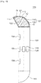
- FIG. 1 is a perspective view showing an odor removal device according to the embodiment of the present invention.
- FIG. 2 is a sectional view showing the odor removal device of FIG. 1 .
- the odor removal device 100 detects the occurrence of odor, and generates active species in the odor-occurring area according to the dielectric barrier discharge principle.
- the active species remove organic matter and kill bacteria, so that odor-causing factors are removed.
- the odor removal device 100 according to the present invention may be used to remove bromhidrosis.
- the odor removal device 100 includes a case 101, an activation device 102, an odor sensing unit 103, a plurality of switches 104 to 106, and a control unit 130.
- the case 101 as a body of the odor removal device 100 is accommodated therein with various devices such as a power source 140 and a control unit 130.
- the case 101 has a shape for enabling a user to hold the case comfortably by hand.
- the case 101 may have one side provided as a curved surface, and the other side provided as a flat surface.
- the activation device 102 may be installed on an upper end of the case 101.
- the activation device 102 comes into contact with the object 20 to generate active species according to the dielectric barrier discharge principle.
- the activation device 102 includes a dielectric 110, an electrode 120.
- the dielectric 110 has a predetermined thickness, and has an inner surface 111 and an outer surface 112.
- the outer surface 112 of the dielectric 110 may be exposed to the outside and provided as curved surfaces.
- the dielectric 110 may have a uniform thickness.
- the electrode 120 is positioned inside the dielectric 110, and the dielectric 110 is provided to surround at least one area of the electrode 120.
- the dielectric 110 may be provided as ceramic, and for example, may be configured to include at least one of alumina (Al2O3), zirconia oxide (ZrO2), germanium (Ge), and cerium (Ce).
- the electrode 120 is applied by power from the power source 140 under the control of the control unit 130.
- the electrode 120 is formed of a metal material.
- the electrode 120 is positioned inside the dielectric 110, and has an outer surface 121 facing the inner surface 111 of the dielectric 110.
- the odor sensing unit 103 may be provided at a lower end of the case 101.
- the odor sensing unit 103 is exposed to the outside, and comes into direct contact with the object 20 to detect the odor generated from the object 20.
- the odor sensing unit 103 may detect the odor caused by fatty organic matter excreted in sweat and bacteria.
- a plurality of switches 104 to 106 are provided, and exposed to the outside of the case 101.
- One switch 104 may be used for controlling an on/off state of the odor removal device 100.
- Another switch 105 may be used as a switch for controlling the application of power to the electrode 120.
- the other switch 106 may be used as a switch for controlling the application of power to the odor sensing unit 103.
- FIG. 3 is a view showing a state in which contact between an activation device and an object according to the embodiment of the present invention
- FIG. 4 is a perspective view showing an electrode of the FIG. 3
- the outer surface 121 of the electrode 120 is provided as a curved surface corresponding to the inner surface 111 of the dielectric 110.
- the outer surface 121 of the electrode 120 includes a contact area A1 in contact with the inner surface 111 of the dielectric 110, and a non-contact area A2 not in contact with the inner surface 111 of the dielectric 110.
- the non-contact area A2 may be positioned in a central area of the outer surface 121 of the electrode 120, and the contact area A1 may be provided to surround the non-contact area A1 around the non-contact area A2.
- the outer surface 121 of the electrode 120 may be formed with a hole or a groove 122 recessed inward to the electrode 120.
- the area formed with the hole or groove 122 is provided as the non-contact area A2 that does not come into contact with the inner surface 111 of the dielectric 110.
- the hole or groove 122 may have the same diameter toward an inner side of the electrode 120. On the contrary, the hole or groove 122 may have the diameter gradually decreased toward the inner side of the electrode 120.
- the power is applied to the electrode 120 while a partial area of the dielectric 110 is in contact with the object 20. Due to the application of power, a streamer is generated along a periphery of the contact point between the dielectric 110 and the object 20.
- the streamer activates surrounding materials such as air. During the activation, active species, electrons, and ions are generated, ultraviolet rays and visible rays are emitted, and an electromagnetic field is generated.
- a current leakage occurs toward the object 20 from an area that is close to the object 20.
- the current leakage occurs at the contact point between the dielectric 110 and the object 20, in which the amount of current leakage is increased as a distance between the electrode 120 and the contact point is decreased.
- the non-contact area A2 is formed on the outer surface of the electrode 120 at a position corresponding to the contact point, so that the occurrence of the current leakage is minimized.
- the dielectric 110 has the central area mainly coming into contact with the object 20, in which the non-contact region A2 of the electrode 120 is positioned in the central area of the dielectric 110. Accordingly, the current leakage to the central area of the dielectric 110 is minimized, and a high energy streamer is generated around the contact area boundary between the dielectric 110 and the object 20, so that the surrounding material can be activated with high energy.
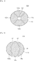
- FIG. 5 is a front view showing an electrode according to another embodiment of the present invention.
- the electrode 120 may be divided into a plurality of electrode pieces 120a to 120d.
- a groove is formed in each of the electrode pieces 120a to 120d.
- the grooves are combined with each other, thereby forming one hole 122.
- the hole 122 is provided as the non-contact area A2.
- the present embodiment shows that the electrode 120 is divided into four electrode pieces 120a to 120d, however, the number of divided pieces may be variously changed.
- FIG. 6 is a front view showing an electrode according to still another embodiment of the present invention.
- the electrode 120 may be divided into a plurality of electrode pieces 120a to 120c.
- the outer surface of the electrode 120 is provided with an interspace A2 between the electrode pieces 120a to 120c, and the interspace A2 is provided as a non-contact area.
- FIG. 7 is a front view showing an electrode according to still another embodiment of the present invention.
- a plurality of non-contact areas A21 and A22 may be formed on the outer surface of the electrode 120.
- the non-contact areas A21 and A22 includes a first area A21 formed in a central area of the outer surface of the electrode 120, and a plurality of second area A22 spaced apart from each other along an outer peripheral area of the electrode 120.
- the first area A21 may have a circular or oval shape.
- the second area A22 may be recessed inward from the periphery of the electrode 120, and have an arc-shaped boundary line with the contact area A1.
- the first area A21 and the second area A22 and the second areas A22 are spaced apart from each other, and a contact area A1 is provided between the above areas.
- the streamer is generated along the boundary between the contact area A1 and the non-contact area A21 and A22.
- FIG. 8 is a front view showing an electrode according to still another embodiment of the present invention.
- the contact area of the electrode 120 includes a first area A11, a second area A12, a third area A13, and a fourth area A14.
- the first area A11 has a circular or oval ring shape and is positioned in the central area of the outer surface of the electrode 120. An inner space of the first area A11 is provided as the non-contact area A21.
- the second area A12 extends from both sides of the first area A11 by a predetermined length in a first direction X.
- the third area A13 extends from an upper end and a lower end of the first area A11 by a predetermined length in a second direction Y perpendicular to the first direction X.
- the third area A13 may have a length shorter than a length of the second area A12.
- the fourth area A14 slantingly extends from the first area A11 at a predetermined angle with respect to the first direction X, in each section between the second area A12 and the third area A13. Sections between the second to fourth areas A12 to A14 are provided as the non-contact area A22.
- FIG. 9 is a front view showing an electrode according to still another embodiment of the present invention.
- the central area of the outer surface of the electrode 120 is provided as the non-contact region A21.
- the contact areas A11 to A13 are provided radially around the non-contact area A21.
- the contact areas A11 to A13 includes a first area A11, a second area A12, and a third area A13.
- the first area A11 extends from both sides of the non-contact area A21 by a predetermined length in the first direction X.
- the second area A12 extends from an upper end and a lower end of the non-contact area A21 by a predetermined length in the second direction Y perpendicular to the first direction X.
- the third area A13 slantingly extends from the non-contact area A21 at a predetermined angle with respect to the first direction X, in each section between the first area A21 and the second area A22.
- a section A22 between the first to third areas A11 to A13 is provided as a non-contact area.
- FIG. 10 is a sectional view showing an electrode according to still another embodiment of the present invention.
- FIG. 11 is a front view showing a contact area between the electrode and the dielectric in FIG. 10 .
- a ring-shaped protrusion 125 is formed on the outer surface of the electrode 120, and the protrusion 125 comes into contact with the dielectric 110. Accordingly, the contact area A1 is formed as a ring shape.
- the electrode 120 may be implemented such that the contact area A1 and the non-contact area A2 with the dielectric 110 have various shapes.
- the non-contact area is positioned at the contact point between the dielectric 110 and the object 20, so that a current leakage can be minimized, and the streamer with high energy are generated in various shapes along the boundary of the contact area, so that the surrounding material can be activated with high energy.
- the odor removal device according to the present invention may be used to suppress a bromhidrosis.
Landscapes
- Health & Medical Sciences (AREA)
- Veterinary Medicine (AREA)
- Life Sciences & Earth Sciences (AREA)
- Animal Behavior & Ethology (AREA)
- General Health & Medical Sciences (AREA)
- Public Health (AREA)
- Engineering & Computer Science (AREA)
- Epidemiology (AREA)
- Biomedical Technology (AREA)
- Nuclear Medicine, Radiotherapy & Molecular Imaging (AREA)
- Radiology & Medical Imaging (AREA)
- Physics & Mathematics (AREA)
- Plasma & Fusion (AREA)
- Disinfection, Sterilisation Or Deodorisation Of Air (AREA)
Abstract
Description
- The present invention relates to an odor removal device, and more particularly, to an odor removal device to come into contact with an object so as to activate surrounding materials according to a dielectric barrier discharge principle.
- bromhidrosis (body odor) refers to an odor caused by fatty organic matter secreted through sweat and bacteria. Currently, chemical compound deodorants are used to remove the odors for cosmetic and etiquette purposes.
- However, controversy over the harmfulness to the human body due to the deodorants for suppressing bromhidrosis is increasing. In particular, the harmfulness of contained chemical ingredients for blocking pores to suppress the secretion of sweat has been raised. In addition to simple dermatitis, breast cancer, deterioration of thyroid functions (triclosan), abnormal sweat secretion hormones due to obstructed sweat glands (aluminum salt), skin damages, and hyperpigmentation may be caused.
- Accordingly, there is a need for odor removal technology capable of suppressing the bromhidrosis without the harmfulness of chemical ingredients.
- The present invention provides an odor removal device capable of suppressing the bromhidrosis without using chemical ingredients.
- The present invention provides an odor removal device capable of activating surrounding materials with high energy.
- The odor removal device according to the present invention includes: a case; an activation device installed in the case and coming into contact with an object to activate surrounding materials according to a dielectric barrier discharge principle, wherein the activation device may include: a dielectric having an outer surface exposed to an outside and provided as a curved surface; and an electrode positioned inside the dielectric in which power is applied to the electrode.
- In addition, the dielectric may have a predetermined thickness, and have an inner surface facing the outer surface, wherein the outer surface of the electrode may include a contact area that comes into contact with the inner surface of the dielectric, and a non-contact area that does not come into contact with the inner surface of the dielectric.
- In addition, the non-contact area may be positioned in a central area of the outer surface of the electrode, and the contact area may surround the non-contact area.
- In addition, the non-contact area may have a circular or oval shape.
- In addition, the contact area may be provided with a plurality of contact areas, spaced apart from each other with the non-contact area therebetween.
- In addition, the odor removal device may include an odor sensing unit installed in the case, and coming into contact with the object to detect an odor.
- According to the present invention, organic matter may be removed and bacteria may be killed from the skin by using active species, so that odor-causing factors can be removed.
- According to the present invention, the non-contact area of the electrode and the dielectric may be positioned at a contact point between the dielectric and the object, so that a current leakage can be minimized, and streamer with high energy may be generated along the boundary of the contact area between the electrode and the dielectric, so that the surrounding materials can be activated with high energy.
- The above and other objects, features, and advantages of the present invention will be more apparent from the following detailed description taken in conjunction with the accompanying drawings, in which:
-
FIG. 1 is a perspective view showing an odor removal device according to the embodiment of the present invention. -
FIG. 2 is a sectional view showing the odor removal device ofFIG. 1 . -
FIG. 3 is a view showing a state in which contact between an activation device and an object according to the embodiment of the present invention. -
FIG. 4 is a perspective view showing an electrode of theFIG. 3 -
FIG. 5 is a front view showing an electrode according to another embodiment of the present invention. -
FIG. 6 is a front view showing an electrode according to still another embodiment of the present invention. -
FIG. 7 is a front view showing an electrode according to still another embodiment of the present invention. -
FIG. 8 is a front view showing an electrode according to still another embodiment of the present invention. -
FIG. 9 is a front view showing an electrode according to still another embodiment of the present invention. -
FIG. 10 is a sectional view showing an electrode according to still another embodiment of the present invention. -
FIG. 11 is a front view showing a contact area between the electrode and the dielectric inFIG. 10 . - An odor removal device according to the present invention includes: a case; an activation device installed in the case and coming into contact with an object to activate surrounding materials according to a dielectric barrier discharge principle, wherein the activation device may include: a dielectric having an outer surface exposed to an outside and provided as a curved surface; and an electrode positioned inside the dielectric in which power is applied to the electrode.
- Hereinafter, preferred embodiments of the present invention will be described in detail with reference to the accompanying drawings. However, the technical idea of the present invention is not limited to the exemplary embodiments described herein and may be embodied in other forms. Further, the embodiments are provided to enable contents disclosed herein to be thorough and complete and provided to enable those skilled in the art to fully understand the idea of the present invention.
- In the specification herein, when one component is mentioned as being on other component, it signifies that the one component may be placed directly on the other component or a third component may be interposed therebetween. In addition, in drawings, thicknesses of layers and areas may be exaggerated to effectively describe the technology of the present invention.
- In addition, although terms such as first, second and third are used to describe various components in various embodiments of the present specification, the components should not be limited by the terms. The above terms are used merely to distinguish one component from another. Accordingly, a first component referred to in one embodiment may be referred to as a second component in another embodiment. Each embodiment described and illustrated herein may also include a complementary embodiment. In addition, the term "and/or" is used herein to include at least one of the components listed before and after the term.
- The singular expression herein includes a plural expression unless the context clearly specifies otherwise. In addition, it will be understood that the term such as "include" or "have" herein is intended to designate the presence of feature, number, step, component, or a combination thereof recited in the specification, and does not preclude the possibility of the presence or addition of one or more other features, numbers, steps, components, or combinations thereof. In addition, the term "connection" is used herein to include both indirectly connecting a plurality of components and directly connecting the components.
- In addition, in the following description of the embodiments of the present invention, the detailed description of known functions and configurations incorporated herein will be omitted when it possibly makes the subject matter of the present invention unclear unnecessarily.
-
FIG. 1 is a perspective view showing an odor removal device according to the embodiment of the present invention.FIG. 2 is a sectional view showing the odor removal device ofFIG. 1 . - Referring to
FIGS. 1 and2 , theodor removal device 100 detects the occurrence of odor, and generates active species in the odor-occurring area according to the dielectric barrier discharge principle. The active species remove organic matter and kill bacteria, so that odor-causing factors are removed. Theodor removal device 100 according to the present invention may be used to remove bromhidrosis. - The
odor removal device 100 includes acase 101, anactivation device 102, anodor sensing unit 103, a plurality ofswitches 104 to 106, and acontrol unit 130. - The
case 101 as a body of theodor removal device 100 is accommodated therein with various devices such as apower source 140 and acontrol unit 130. Thecase 101 has a shape for enabling a user to hold the case comfortably by hand. According to the embodiment, thecase 101 may have one side provided as a curved surface, and the other side provided as a flat surface. - The
activation device 102 may be installed on an upper end of thecase 101. Theactivation device 102 comes into contact with theobject 20 to generate active species according to the dielectric barrier discharge principle. Theactivation device 102 includes a dielectric 110, anelectrode 120. - The dielectric 110 has a predetermined thickness, and has an
inner surface 111 and anouter surface 112. Theouter surface 112 of the dielectric 110 may be exposed to the outside and provided as curved surfaces. The dielectric 110 may have a uniform thickness. Theelectrode 120 is positioned inside the dielectric 110, and the dielectric 110 is provided to surround at least one area of theelectrode 120. The dielectric 110 may be provided as ceramic, and for example, may be configured to include at least one of alumina (Al2O3), zirconia oxide (ZrO2), germanium (Ge), and cerium (Ce). - The
electrode 120 is applied by power from thepower source 140 under the control of thecontrol unit 130. Theelectrode 120 is formed of a metal material. Theelectrode 120 is positioned inside the dielectric 110, and has anouter surface 121 facing theinner surface 111 of the dielectric 110. - The
odor sensing unit 103 may be provided at a lower end of thecase 101. Theodor sensing unit 103 is exposed to the outside, and comes into direct contact with theobject 20 to detect the odor generated from theobject 20. Theodor sensing unit 103 may detect the odor caused by fatty organic matter excreted in sweat and bacteria. - A plurality of
switches 104 to 106 are provided, and exposed to the outside of thecase 101. Oneswitch 104 may be used for controlling an on/off state of theodor removal device 100. Anotherswitch 105 may be used as a switch for controlling the application of power to theelectrode 120. Theother switch 106 may be used as a switch for controlling the application of power to theodor sensing unit 103. - Hereinafter, referring
Figs 3 to 11 , theactivation device 10 will be described in detail. -
FIG. 3 is a view showing a state in which contact between an activation device and an object according to the embodiment of the present invention,FIG. 4 is a perspective view showing an electrode of theFIG. 3 - Referring to
FIGS. 1 to 4 , Theouter surface 121 of theelectrode 120 is provided as a curved surface corresponding to theinner surface 111 of the dielectric 110. Theouter surface 121 of theelectrode 120 includes a contact area A1 in contact with theinner surface 111 of the dielectric 110, and a non-contact area A2 not in contact with theinner surface 111 of the dielectric 110. The non-contact area A2 may be positioned in a central area of theouter surface 121 of theelectrode 120, and the contact area A1 may be provided to surround the non-contact area A1 around the non-contact area A2. - According to one example, the
outer surface 121 of theelectrode 120 may be formed with a hole or agroove 122 recessed inward to theelectrode 120. The area formed with the hole or groove 122 is provided as the non-contact area A2 that does not come into contact with theinner surface 111 of the dielectric 110. The hole or groove 122 may have the same diameter toward an inner side of theelectrode 120. On the contrary, the hole or groove 122 may have the diameter gradually decreased toward the inner side of theelectrode 120. - The power is applied to the
electrode 120 while a partial area of the dielectric 110 is in contact with theobject 20. Due to the application of power, a streamer is generated along a periphery of the contact point between the dielectric 110 and theobject 20. The streamer activates surrounding materials such as air. During the activation, active species, electrons, and ions are generated, ultraviolet rays and visible rays are emitted, and an electromagnetic field is generated. - Meanwhile, in the
electrode 120, a current leakage occurs toward theobject 20 from an area that is close to theobject 20. The current leakage occurs at the contact point between the dielectric 110 and theobject 20, in which the amount of current leakage is increased as a distance between theelectrode 120 and the contact point is decreased. - The present invention the non-contact area A2 is formed on the outer surface of the
electrode 120 at a position corresponding to the contact point, so that the occurrence of the current leakage is minimized. Specifically, the dielectric 110 has the central area mainly coming into contact with theobject 20, in which the non-contact region A2 of theelectrode 120 is positioned in the central area of the dielectric 110. Accordingly, the current leakage to the central area of the dielectric 110 is minimized, and a high energy streamer is generated around the contact area boundary between the dielectric 110 and theobject 20, so that the surrounding material can be activated with high energy. -
FIG. 5 is a front view showing an electrode according to another embodiment of the present invention. - Referring to
FIG. 5 , theelectrode 120 may be divided into a plurality ofelectrode pieces 120a to 120d. A groove is formed in each of theelectrode pieces 120a to 120d. When theelectrode pieces 120a to 120d are combined, the grooves are combined with each other, thereby forming onehole 122. Thehole 122 is provided as the non-contact area A2. The present embodiment shows that theelectrode 120 is divided into fourelectrode pieces 120a to 120d, however, the number of divided pieces may be variously changed. -
FIG. 6 is a front view showing an electrode according to still another embodiment of the present invention. - Referring to
FIG. 6 , theelectrode 120 may be divided into a plurality ofelectrode pieces 120a to 120c. The outer surface of theelectrode 120 is provided with an interspace A2 between theelectrode pieces 120a to 120c, and the interspace A2 is provided as a non-contact area. -
FIG. 7 is a front view showing an electrode according to still another embodiment of the present invention. - Referring to
FIG. 7 , a plurality of non-contact areas A21 and A22 may be formed on the outer surface of theelectrode 120. Specifically, the non-contact areas A21 and A22 includes a first area A21 formed in a central area of the outer surface of theelectrode 120, and a plurality of second area A22 spaced apart from each other along an outer peripheral area of theelectrode 120. The first area A21 may have a circular or oval shape. The second area A22 may be recessed inward from the periphery of theelectrode 120, and have an arc-shaped boundary line with the contact area A1. The first area A21 and the second area A22 and the second areas A22 are spaced apart from each other, and a contact area A1 is provided between the above areas. The streamer is generated along the boundary between the contact area A1 and the non-contact area A21 and A22. -
FIG. 8 is a front view showing an electrode according to still another embodiment of the present invention. - Referring to
FIG. 8 , the contact area of theelectrode 120 includes a first area A11, a second area A12, a third area A13, and a fourth area A14. - The first area A11 has a circular or oval ring shape and is positioned in the central area of the outer surface of the
electrode 120. An inner space of the first area A11 is provided as the non-contact area A21. The second area A12 extends from both sides of the first area A11 by a predetermined length in a first direction X. The third area A13 extends from an upper end and a lower end of the first area A11 by a predetermined length in a second direction Y perpendicular to the first direction X. The third area A13 may have a length shorter than a length of the second area A12. The fourth area A14 slantingly extends from the first area A11 at a predetermined angle with respect to the first direction X, in each section between the second area A12 and the third area A13. Sections between the second to fourth areas A12 to A14 are provided as the non-contact area A22. -
FIG. 9 is a front view showing an electrode according to still another embodiment of the present invention. - Referring to
FIG. 9 , the central area of the outer surface of theelectrode 120 is provided as the non-contact region A21. The contact areas A11 to A13 are provided radially around the non-contact area A21. Specifically, the contact areas A11 to A13 includes a first area A11, a second area A12, and a third area A13. - The first area A11 extends from both sides of the non-contact area A21 by a predetermined length in the first direction X. The second area A12 extends from an upper end and a lower end of the non-contact area A21 by a predetermined length in the second direction Y perpendicular to the first direction X. The third area A13 slantingly extends from the non-contact area A21 at a predetermined angle with respect to the first direction X, in each section between the first area A21 and the second area A22. A section A22 between the first to third areas A11 to A13 is provided as a non-contact area.
-
FIG. 10 is a sectional view showing an electrode according to still another embodiment of the present invention.FIG. 11 is a front view showing a contact area between the electrode and the dielectric inFIG. 10 . - Referring to
FIGS. 10 and11 , a ring-shapedprotrusion 125 is formed on the outer surface of theelectrode 120, and theprotrusion 125 comes into contact with the dielectric 110. Accordingly, the contact area A1 is formed as a ring shape. - As described above, the
electrode 120 according to the embodiments of the present invention may be implemented such that the contact area A1 and the non-contact area A2 with the dielectric 110 have various shapes. In addition, the non-contact area is positioned at the contact point between the dielectric 110 and theobject 20, so that a current leakage can be minimized, and the streamer with high energy are generated in various shapes along the boundary of the contact area, so that the surrounding material can be activated with high energy. - Although the present invention has been described in detail with reference to the exemplary embodiments, the present invention is not limited to the specific embodiments and will be interpreted by the following claims. In addition, it will be apparent that a person having ordinary skill in the art may carry out various deformations and modifications for the embodiments described as above within the scope without departing from the present invention.
- The odor removal device according to the present invention may be used to suppress a bromhidrosis.
Claims (6)
- An odor removal device includes:a case;an activation device installed in the case and coming into contact with an object to activate surrounding materials according to a dielectric barrier discharge principle,wherein the activation device includes:a dielectric having an outer surface exposed to an outside and provided as a curved surface; andan electrode positioned inside the dielectric in which power is applied to the electrode.
- The odor removal device of claim 1, the dielectric has a predetermined thickness, and has an inner surface facing the outer surface,
wherein the outer surface of the electrode includes a contact area that comes into contact with the inner surface of the dielectric, and a non-contact area that does not come into contact with the inner surface of the dielectric. - The odor removal device of claim 2, the non-contact area is positioned in a central area of the outer surface of the electrode, and the contact area surrounds the non-contact area.
- The odor removal device of claim 2, the non-contact area has a circular or oval shape.
- The odor removal device of claim 2, the contact area is provided with a plurality of contact areas, spaced apart from each other with the non-contact area therebetween.
- The odor removal device of claim 1, wherein the odor removal device further includes an odor sensing unit installed in the case, and coming into contact with the object to detect an odor.
Applications Claiming Priority (2)
| Application Number | Priority Date | Filing Date | Title |
|---|---|---|---|
| KR1020190123219A KR102320291B1 (en) | 2019-10-04 | 2019-10-04 | Apparatus for removing odor |
| PCT/KR2020/002744 WO2021066264A1 (en) | 2019-10-04 | 2020-02-26 | Deodorizing device |
Publications (2)
| Publication Number | Publication Date |
|---|---|
| EP4062969A1 true EP4062969A1 (en) | 2022-09-28 |
| EP4062969A4 EP4062969A4 (en) | 2023-12-27 |
Family
ID=75336589
Family Applications (1)
| Application Number | Title | Priority Date | Filing Date |
|---|---|---|---|
| EP20871169.7A Pending EP4062969A4 (en) | 2019-10-04 | 2020-02-26 | DEODORIZING DEVICE |
Country Status (4)
| Country | Link |
|---|---|
| US (1) | US20240075181A1 (en) |
| EP (1) | EP4062969A4 (en) |
| KR (1) | KR102320291B1 (en) |
| WO (1) | WO2021066264A1 (en) |
Family Cites Families (13)
| Publication number | Priority date | Publication date | Assignee | Title |
|---|---|---|---|---|
| JP6100613B2 (en) * | 2007-04-19 | 2017-03-22 | ミラマー ラブズ, インコーポレイテッド | Method and apparatus for reducing sweat production |
| US10300159B2 (en) * | 2011-05-05 | 2019-05-28 | Max-Planck-Gesellschaft Zur Foerderung Der Wissenschaften E.V. | Method for deactivating preferably odor-relevant molecules and device for carrying out said method |
| KR101407672B1 (en) * | 2013-07-30 | 2014-06-13 | 주식회사 다온비티아이 | Plasma Skin Treatment Apparatus |
| KR101622143B1 (en) * | 2013-10-30 | 2016-05-18 | 주식회사 화니메디칼 | High Frequency Stimulating Apparatus for Treatment of Skin Texture or Removal of Subcutaneous Fat |
| KR20160124316A (en) * | 2015-04-16 | 2016-10-27 | (주) 프라바이오 | Plasma skin treatment apparatus |
| US20180126183A1 (en) * | 2015-05-29 | 2018-05-10 | Koninklijke Philips N.V. | A device for treating skin using non-thermal plasma |
| KR101794048B1 (en) * | 2016-04-07 | 2017-11-08 | 한국기계연구원 | Flexible active species generator and use thereof |
| KR20180003379A (en) * | 2016-06-30 | 2018-01-09 | (주)프로스테믹스 | Apparatus for promoting hair growth using plasma and uses thereof |
| KR101866545B1 (en) * | 2016-11-02 | 2018-06-11 | 배준형 | Plasma sterilizer grnerating active species using a plurality pole type electrodes and dielectric tubes |
| KR20180136617A (en) * | 2017-06-14 | 2018-12-26 | (주)디지링크 | A portable, drying, sterilizing equipment, and take over the control methods |
| KR102127038B1 (en) * | 2017-11-16 | 2020-06-25 | 광운대학교 산학협력단 | Wearable Plasma Clothes |
| KR102164945B1 (en) * | 2017-12-07 | 2020-10-13 | 배준형 | Apparatus for sterilization and deodorization of air using Plasma and Photocatalyst |
| KR101998158B1 (en) * | 2019-01-28 | 2019-07-09 | (주) 위드닉스 | Dual Head Plasma Device Providing Micro Current |
-
2019
- 2019-10-04 KR KR1020190123219A patent/KR102320291B1/en active Active
-
2020
- 2020-02-26 US US17/766,274 patent/US20240075181A1/en active Pending
- 2020-02-26 WO PCT/KR2020/002744 patent/WO2021066264A1/en not_active Ceased
- 2020-02-26 EP EP20871169.7A patent/EP4062969A4/en active Pending
Also Published As
| Publication number | Publication date |
|---|---|
| KR20210040667A (en) | 2021-04-14 |
| EP4062969A4 (en) | 2023-12-27 |
| KR102320291B1 (en) | 2021-11-02 |
| US20240075181A1 (en) | 2024-03-07 |
| WO2021066264A1 (en) | 2021-04-08 |
Similar Documents
| Publication | Publication Date | Title |
|---|---|---|
| JP6495313B2 (en) | Apparatus for treating a surface with plasma | |
| US10357580B2 (en) | Electrode arrangement for forming a dielectric barrier plasma discharge | |
| TW353621B (en) | A medical device | |
| ES2592170T3 (en) | Electrode system for a barrier plasma | |
| CN105722552A (en) | Device for treating a body surface of a living body | |
| NO20032363D0 (en) | Dosage device for modified release | |
| CN106723866B (en) | Depilator | |
| JPWO2016021234A1 (en) | Endoscope tip structure | |
| US9687292B2 (en) | Electrosurgery handpiece/pencil with smoke evacuation | |
| US20240075181A1 (en) | Odor removal device | |
| BR102015006699A2 (en) | system to distribute a fluid product that is packaged in a tank | |
| US20230371998A1 (en) | Devices and Methods For Treatment Of Skin Conditions | |
| KR102532241B1 (en) | applicator device | |
| KR200455838Y1 (en) | Cap of cosmetic tube container | |
| US20230063183A1 (en) | Activation device and odor removal device including same | |
| JP4442637B2 (en) | Optical hair removal equipment | |
| CN119486779A (en) | Microneedle patch with improved deformability and microneedle patch set including the same | |
| US9630768B2 (en) | Dispensing head for a system for dispensing a product | |
| US10849401B2 (en) | Handheld device for performing an action dependent on an angular position of the device | |
| US9153426B2 (en) | Devices and methods for facilitating treatment of electrospray columns | |
| EP1988757A3 (en) | DBD plasma discharged static eliminator | |
| PT1335701E (en) | ANTI-ADIPOSAL COMPOSITION BASED ON EXTRACTS OF GARLIC BULBS AND COSMETIC AND THERAPEUTIC UTILIZATIONS OF THE SAME | |
| AR117231A1 (en) | HIGHLY ACTIVE AND HIGHLY SELECTIVE EXTRUDED COPPER CATALYSTS | |
| US9931655B2 (en) | Module for dispensing a product intended to be mounted on a pressurized supply duct for said product | |
| EP4649967A1 (en) | Electronic deodorant device using plasma |
Legal Events
| Date | Code | Title | Description |
|---|---|---|---|
| STAA | Information on the status of an ep patent application or granted ep patent |
Free format text: STATUS: THE INTERNATIONAL PUBLICATION HAS BEEN MADE |
|
| PUAI | Public reference made under article 153(3) epc to a published international application that has entered the european phase |
Free format text: ORIGINAL CODE: 0009012 |
|
| STAA | Information on the status of an ep patent application or granted ep patent |
Free format text: STATUS: REQUEST FOR EXAMINATION WAS MADE |
|
| 17P | Request for examination filed |
Effective date: 20220725 |
|
| AK | Designated contracting states |
Kind code of ref document: A1 Designated state(s): AL AT BE BG CH CY CZ DE DK EE ES FI FR GB GR HR HU IE IS IT LI LT LU LV MC MK MT NL NO PL PT RO RS SE SI SK SM TR |
|
| DAV | Request for validation of the european patent (deleted) | ||
| DAX | Request for extension of the european patent (deleted) | ||
| A4 | Supplementary search report drawn up and despatched |
Effective date: 20231128 |
|
| RIC1 | Information provided on ipc code assigned before grant |
Ipc: A61L 2/14 20060101ALI20231122BHEP Ipc: A61L 2/00 20060101ALI20231122BHEP Ipc: A61L 9/22 20060101ALI20231122BHEP Ipc: A61N 1/04 20060101ALI20231122BHEP Ipc: A61N 1/44 20060101AFI20231122BHEP |
|
| GRAP | Despatch of communication of intention to grant a patent |
Free format text: ORIGINAL CODE: EPIDOSNIGR1 |
|
| STAA | Information on the status of an ep patent application or granted ep patent |
Free format text: STATUS: GRANT OF PATENT IS INTENDED |
|
| RIC1 | Information provided on ipc code assigned before grant |
Ipc: A61N 1/44 20060101AFI20260128BHEP Ipc: A61N 1/04 20060101ALI20260128BHEP Ipc: A61L 9/22 20060101ALI20260128BHEP Ipc: A61L 2/00 20060101ALI20260128BHEP Ipc: A61L 2/14 20060101ALI20260128BHEP |
|
| INTG | Intention to grant announced |
Effective date: 20260218 |
|
| GRAS | Grant fee paid |
Free format text: ORIGINAL CODE: EPIDOSNIGR3 |
|
| GRAA | (expected) grant |
Free format text: ORIGINAL CODE: 0009210 |
|
| STAA | Information on the status of an ep patent application or granted ep patent |
Free format text: STATUS: THE PATENT HAS BEEN GRANTED |