EP4060355B1 - Schutz des inhalts eines schmelzspeichers - Google Patents
Schutz des inhalts eines schmelzspeichers Download PDFInfo
- Publication number
- EP4060355B1 EP4060355B1 EP22162199.8A EP22162199A EP4060355B1 EP 4060355 B1 EP4060355 B1 EP 4060355B1 EP 22162199 A EP22162199 A EP 22162199A EP 4060355 B1 EP4060355 B1 EP 4060355B1
- Authority
- EP
- European Patent Office
- Prior art keywords
- state
- circuit
- word
- fuse
- memory
- Prior art date
- Legal status (The legal status is an assumption and is not a legal conclusion. Google has not performed a legal analysis and makes no representation as to the accuracy of the status listed.)
- Active
Links
- 230000015654 memory Effects 0.000 title claims description 59
- 238000012360 testing method Methods 0.000 claims description 35
- 230000007704 transition Effects 0.000 claims description 26
- 238000012545 processing Methods 0.000 claims description 25
- 238000000034 method Methods 0.000 claims description 20
- 238000012795 verification Methods 0.000 claims description 14
- 230000001143 conditioned effect Effects 0.000 claims description 2
- 238000004519 manufacturing process Methods 0.000 description 13
- 230000007547 defect Effects 0.000 description 9
- 230000008901 benefit Effects 0.000 description 6
- 230000006870 function Effects 0.000 description 4
- 230000009471 action Effects 0.000 description 3
- 239000004020 conductor Substances 0.000 description 3
- 238000003066 decision tree Methods 0.000 description 3
- 238000013461 design Methods 0.000 description 3
- 230000008569 process Effects 0.000 description 3
- 230000003466 anti-cipated effect Effects 0.000 description 2
- 230000002427 irreversible effect Effects 0.000 description 2
- 238000012423 maintenance Methods 0.000 description 2
- 239000000615 nonconductor Substances 0.000 description 2
- 230000001960 triggered effect Effects 0.000 description 2
- 206010010904 Convulsion Diseases 0.000 description 1
- 201000000251 Locked-in syndrome Diseases 0.000 description 1
- 230000008859 change Effects 0.000 description 1
- 230000003750 conditioning effect Effects 0.000 description 1
- 238000001514 detection method Methods 0.000 description 1
- 230000014509 gene expression Effects 0.000 description 1
- 230000007257 malfunction Effects 0.000 description 1
- 239000000463 material Substances 0.000 description 1
- 230000007246 mechanism Effects 0.000 description 1
- 230000002441 reversible effect Effects 0.000 description 1
- 230000035945 sensitivity Effects 0.000 description 1
- 238000012956 testing procedure Methods 0.000 description 1
Images


Classifications
-
- G—PHYSICS
- G01—MEASURING; TESTING
- G01R—MEASURING ELECTRIC VARIABLES; MEASURING MAGNETIC VARIABLES
- G01R31/00—Arrangements for testing electric properties; Arrangements for locating electric faults; Arrangements for electrical testing characterised by what is being tested not provided for elsewhere
- G01R31/28—Testing of electronic circuits, e.g. by signal tracer
- G01R31/317—Testing of digital circuits
- G01R31/31719—Security aspects, e.g. preventing unauthorised access during test
-
- G—PHYSICS
- G11—INFORMATION STORAGE
- G11C—STATIC STORES
- G11C29/00—Checking stores for correct operation ; Subsequent repair; Testing stores during standby or offline operation
- G11C29/52—Protection of memory contents; Detection of errors in memory contents
-
- G—PHYSICS
- G01—MEASURING; TESTING
- G01R—MEASURING ELECTRIC VARIABLES; MEASURING MAGNETIC VARIABLES
- G01R31/00—Arrangements for testing electric properties; Arrangements for locating electric faults; Arrangements for electrical testing characterised by what is being tested not provided for elsewhere
- G01R31/28—Testing of electronic circuits, e.g. by signal tracer
- G01R31/317—Testing of digital circuits
- G01R31/3181—Functional testing
- G01R31/3185—Reconfiguring for testing, e.g. LSSD, partitioning
- G01R31/318533—Reconfiguring for testing, e.g. LSSD, partitioning using scanning techniques, e.g. LSSD, Boundary Scan, JTAG
- G01R31/318583—Design for test
- G01R31/318588—Security aspects
-
- G—PHYSICS
- G06—COMPUTING; CALCULATING OR COUNTING
- G06F—ELECTRIC DIGITAL DATA PROCESSING
- G06F1/00—Details not covered by groups G06F3/00 - G06F13/00 and G06F21/00
- G06F1/24—Resetting means
-
- G—PHYSICS
- G06—COMPUTING; CALCULATING OR COUNTING
- G06F—ELECTRIC DIGITAL DATA PROCESSING
- G06F9/00—Arrangements for program control, e.g. control units
- G06F9/06—Arrangements for program control, e.g. control units using stored programs, i.e. using an internal store of processing equipment to receive or retain programs
- G06F9/44—Arrangements for executing specific programs
- G06F9/448—Execution paradigms, e.g. implementations of programming paradigms
- G06F9/4498—Finite state machines
-
- G—PHYSICS
- G11—INFORMATION STORAGE
- G11C—STATIC STORES
- G11C29/00—Checking stores for correct operation ; Subsequent repair; Testing stores during standby or offline operation
- G11C29/02—Detection or location of defective auxiliary circuits, e.g. defective refresh counters
- G11C29/027—Detection or location of defective auxiliary circuits, e.g. defective refresh counters in fuses
-
- G—PHYSICS
- G11—INFORMATION STORAGE
- G11C—STATIC STORES
- G11C29/00—Checking stores for correct operation ; Subsequent repair; Testing stores during standby or offline operation
- G11C29/04—Detection or location of defective memory elements, e.g. cell constructio details, timing of test signals
- G11C29/08—Functional testing, e.g. testing during refresh, power-on self testing [POST] or distributed testing
- G11C29/10—Test algorithms, e.g. memory scan [MScan] algorithms; Test patterns, e.g. checkerboard patterns
-
- G—PHYSICS
- G11—INFORMATION STORAGE
- G11C—STATIC STORES
- G11C29/00—Checking stores for correct operation ; Subsequent repair; Testing stores during standby or offline operation
- G11C29/04—Detection or location of defective memory elements, e.g. cell constructio details, timing of test signals
- G11C29/50—Marginal testing, e.g. race, voltage or current testing
-
- G—PHYSICS
- G11—INFORMATION STORAGE
- G11C—STATIC STORES
- G11C29/00—Checking stores for correct operation ; Subsequent repair; Testing stores during standby or offline operation
- G11C29/54—Arrangements for designing test circuits, e.g. design for test [DFT] tools
-
- G—PHYSICS
- G01—MEASURING; TESTING
- G01R—MEASURING ELECTRIC VARIABLES; MEASURING MAGNETIC VARIABLES
- G01R31/00—Arrangements for testing electric properties; Arrangements for locating electric faults; Arrangements for electrical testing characterised by what is being tested not provided for elsewhere
- G01R31/28—Testing of electronic circuits, e.g. by signal tracer
- G01R31/317—Testing of digital circuits
- G01R31/3181—Functional testing
- G01R31/3185—Reconfiguring for testing, e.g. LSSD, partitioning
- G01R31/318533—Reconfiguring for testing, e.g. LSSD, partitioning using scanning techniques, e.g. LSSD, Boundary Scan, JTAG
- G01R31/318597—JTAG or boundary scan test of memory devices
-
- G—PHYSICS
- G11—INFORMATION STORAGE
- G11C—STATIC STORES
- G11C29/00—Checking stores for correct operation ; Subsequent repair; Testing stores during standby or offline operation
- G11C29/04—Detection or location of defective memory elements, e.g. cell constructio details, timing of test signals
- G11C29/08—Functional testing, e.g. testing during refresh, power-on self testing [POST] or distributed testing
- G11C29/12—Built-in arrangements for testing, e.g. built-in self testing [BIST] or interconnection details
- G11C2029/1206—Location of test circuitry on chip or wafer
Definitions
- the present description generally concerns electronic circuits, and more particularly integrated circuits comprising a non-volatile fuse-type memory.
- the present description concerns, in particular, the implementation of a method making it possible to carry out a test of such a circuit.
- Integrated circuits are used in the design of electronic devices with various applications.
- JTAG Joint Test Action Group
- the JTAG interface is commonly used to test memories, particularly non-volatile memories, and is likely to be used in production as well as in the life of the product, particularly during maintenance operations in order to identify potential defects from manufacturing.
- the integrated circuit is then generally returned to the manufacturer.
- users may wish to return the product to the manufacturer so that it can be retested for manufacturing defects.
- the user does not perform these tests as routine maintenance.
- the user notices a problem, suspects it might be a manufacturing defect, and returns the product so the manufacturer can rerun a scan test to analyze the defect.
- Testing procedures and access to information contained in the memories of an integrated circuit are likely to pose problems in applications where these memories contain information intended to be hidden from the manufacturer.
- These may be authentication or encryption keys (more generally passwords, codes or keys used in the life of the circuit), software codes or proprietary protocols stored in the circuit during a personalization phase carried out. by the end user of the circuit or by an intermediary entity between the manufacturer and this user.
- These elements constitute information to be hidden from the manufacturer (secrets), which it is generally not desirable to communicate to the manufacturer of the integrated circuit.
- non-volatile memories of the circuit are of the erasable or reprogrammable type (flash memory or EPROM), it is possible to erase areas of the memory containing the "secret" before returning the circuit for fault analysis.
- flash memory erasable or reprogrammable type
- EPROM erasable or reprogrammable type
- the non-volatile memories are of the fuse type, their programming is irreversible and it is then problematic to allow access to the circuit via its JTAG interface when performing operational tests of the components of the circuit.
- One embodiment overcomes all or part of the drawbacks of known integrated circuit devices.
- One embodiment provides a method in which a state of an integrated circuit enters a first state, authorizing access for reading of a first area of a memory not volatile fuse type to a processing unit, and a second state, prohibiting access for reading of said memory to the processing unit, is conditioned by a verification, by a finite state machine, of a first word of fuse type of said memory, representing a number of transitions to said first state, and a second fuse type word of said memory, representing a number of transitions to said second state.
- One embodiment provides an integrated circuit comprising a finite state machine configured to condition a state of the integrated circuit between a first state, authorizing access for reading of a first area of a non-volatile fuse-type memory to a unit processing, and a second state, prohibiting access for reading of said memory to the processing unit, to a verification of the values of a first fuse-type word of said memory, representing a number of transitions to said first state , and a second fuse type word of said memory, representing a number of transitions to said second state.
- said verification consists of comparing the respective values of said first and second words and of verifying the value of the most significant bit of the first word.
- the circuit is in the first state if the value of the second word is lower than the value of the first word or if the most significant bit of the first word is burned out.
- said verification is carried out each time the integrated circuit is reset.
- a scanning test of the integrated circuit is prohibited.
- a scanning test of the integrated circuit is permitted, except for the fuse-type non-volatile memory.
- an increment of the second counter is caused exclusively by the state machine.
- an increment of the first counter is accessible to the processing unit.
- a transition of said circuit from the first state to the second state is carried out if, and only if, upon exiting from reset, a value entered into a register from outside the circuit while said circuit is being reset, corresponds to a code stored in said first zone of the non-volatile fuse-type memory, said code being only readable by the finite state machine.
- any introduction of a value into said register when the integrated circuit is in the first state upon exiting from reset, increments a third counter defined by a third word of said memory provided that the most significant bit of said third word is different from 1.
- FIG 1 represents, very schematically and in block form, an embodiment of an integrated circuit device of the type to which the described embodiments apply, by way of example;
- figure 2 represents, schematically and in the form of blocks, more detailed than in figure 1 , an embodiment of an integrated circuit of the type to which, by way of example, the embodiments described apply;
- FIG. 3 is a decision tree illustrating a mode of implementation of a method for protecting the contents of a fuse memory
- FIG. 4 is a flowchart representing steps of a mode of implementing a transition to a scanning test mode of an integrated circuit.
- the expressions “approximately”, “approximately”, “substantially”, and “of the order of” mean to the nearest 10%, preferably to the nearest 5%.
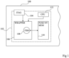
- FIG. 1 represents, very schematically and in block form, an embodiment of an electronic device 100 comprising an integrated circuit 102 of the type to which the described embodiments apply, by way of example.
- the electronic device is, for example, an electronic card such as a microcircuit card, hardware for computer use, a microprocessor circuit, etc.
- the integrated circuit 102 comprises a non-volatile, non-rewritable memory, of fuse type (FUSE NV MEM) 110.
- FUSE NV MEM fuse type
- all the bits of fuse type of memory 110 are in the same state, arbitrarily 0. This state corresponds, depending on the native state of the fuse bits, for example, to a non-conductive or "blocked" state, of the storage elements defining the bits.
- data is stored on the non-volatile memory 110 by switching the states of (by burning) certain bits of the memory (memory words) towards the reverse state 1, corresponding for example to a conductive or “on” state of the corresponding storage elements.
- the integrated circuit 102 further comprises a processing unit (CPU) 112, having access to the memory 110 via an adapter 106 (WRAPPER).
- the integrated circuit 102 further comprises a JTAG (Joint Test Action Group) type access port 104 allowing a user to connect a JTAG type interface (not shown) to the circuit in order to request the running system tests. These tests are, for example, circuit continuity tests detecting possible short circuits or even tests of the logic functions of the circuit. Tests cannot be carried out during the design of prototypes, during manufacturing, or even when the device 100 is returned to the manufacturer for analysis of defect(s).
- the embodiments described provide a new mechanism for authorizing access to the integrated circuit during tests, without compromising the security of this data.
- the circuit will have, particularly from the point of view of the JTAG port 104, a "closed” state in which the scanning tests are blocked but in which the adapter 106 authorizes the processing unit 112 to have access to the memory 110, including its protected part (202, Fig. 2 ) containing the "secret”, and an "open” state in which the scanning tests are permitted, but in which the adapter 106 prohibits any access to the protected area 202 of the memory 110 to the processing unit 112 and that even through scanning tests.
- the embodiments described provide for the presence of a finite state machine (FSM) 108 to control the transition from the "closed" state of the circuit to the "open” state.
- FSM finite state machine
- the adapter 106 contained in the circuit 102, ensures compatibility between data that can be entered via the JTAG interface and the data stored in the non-volatile non-rewritable memory 110.
- the adapter 106 itself contains the finite state machine 108 and is connected to the access port 104 and to the non-volatile memory 110.
- the JTAG access port 104 is not connected to the processing unit 112 and, in In particular, the respective operations of the processor 112 and the finite state machine 108 are independent of each other.
- figure 2 represents, schematically and in the form of blocks, more detailed than in figure 1 , an embodiment of an integrated circuit of the type to which the described embodiments apply, by way of example.
- the fuse-type non-volatile memory 110 comprises or is broken down into several distinct memory zones.
- a first zone (PROTECTED) 202 contains all the data (program or data itself) to which access must be reserved for operation in a secure mode or environment, that is to say when the circuit is in the closed state.
- This data is stored by the end user of the circuit or by an intermediary entity between the manufacturer and this user.
- This data may be authentication or encryption keys, software codes or proprietary protocols, etc.
- codes or passwords are contained in dedicated memory words 204. This or these codes are used in particular to condition the reopening of the circuit.
- the code 204 is only readable by the adapter 106 and, more particularly, by the state machine 108.
- the code 204 can be stored in the zone 202 by the manufacturer during the production of the circuit 102, but is preferably chosen and stored during the personalization phase.
- Code 204 corresponds to a secret fuse-type password which, once programmed (or locked), is only accessible by finite state machine 108.
- the state machine 108 determines whether the chip is in an “open” state or in a “closed” state. If the chip is in a "closed” state, and if content has been entered into a register 206 of the adapter 106 before the chip comes out of reset, the finite state machine compares the code 204 with this content. During the period in which the chip is resetting, JTAG access port 104 is functional and content can be entered and is then stored in register 206.
- Register 206 accessible via JTAG port 104, is typically a shift register (volatile storage) written via JTAG port and read by state machine 108. Writing of the register is carried out, in the usual manner, by a input TDI data by being sequenced by a TCK signal from the JTAG interface.
- the function 109 for comparing the data entered via port 104 and that contained in code 204 is also part of the finite state machine.
- a second zone is provided in the memory 110 containing first, second and third memory words 208 (WORD1), 210 (WORD2) and 212 (WORD3) having specific functions linked to the opening and closing of the circuit. More particularly, each word 208, 210, 212 constitutes a counter, respectively, of the number of closures, the number of openings and the number of seizures of data via port 104 when the chip is in reset. Initially, all fuse bits of words 208, 210 and 212 are in the same state, arbitrarily 0. Word 210 can only be burned by state machine 108 (and not by unit 112).
- each word 208, 210, 212 may be the same or different from one word to another. This length conditions, depending on the word, the number of closures, openings and password entry attempts via the JTAG interface.
- each word 208, 210, 212 comprises at least 8 bits, preferably 32 bits.
- the bits of words 208 to 212 are irreversibly programmable bits, the corresponding counter does not count a number which can reach 2 raised to the power of the number of bits, but a number which can reach at most the number of bits.
- the state machine 108 burns a bit (or group of bits) of the counter represented by the word 212. This uses one of the opportunities to guess the password.
- circuit 102 is locked in state "farm". For example, in the case where word 212 is composed of 8 bits (or 32 bits programmed in groups of 4 bits), the circuit is locked after eight attempts to enter a password via the JTAG interface.
- the circuit except for the non-volatile fuse-type memory 110, can then be subject to a scanning test.
- An "open” chip can be "closed” at any time by burning a bit (or a group of bits) of the counter represented by word 208. This operation can be performed by the processing unit 112 or by an attached debugger to JTAG port 104.
- Closing the circuit involves burning a bit of word 208, thus using an opportunity to close the circuit. If all bits in word 208 are burned out, the circuit is stuck in the closed state and cannot be opened again.
- counters 208 and 210 are provided. Indeed, counter 212 only prevents a brutal password guessing attack. This is useful if the 204 password is short.
- an advantage induced by the implementation of reopenings by the state machine 108 rather than by the processing unit 112 is that the fact of reopening to carry out scanning tests will work even when the manufacturing defect is in the processing unit 112 itself.
- the processing unit 112 occupies a significant surface area of the circuit 102, particularly compared to the size of the state machine 108, and the probability that the fault which caused the malfunction of the circuit is present there is not negligible. .
- FIG. 3 is a decision tree illustrating a mode of implementation of a method of protecting the contents of a fuse memory.
- Figure 3 is a decision tree representing the conditions at which the circuit 102 is in the open state, respectively in the closed state.
- the finite state machine 108 checks the state (open or closed) in which circuit 102 is located. The state is determined by the values respective of the first, second and third words 208, 210 and 212.
- the checks of the respective counters represented by the words 208, 210 and 212 are carried out by determining the rank of the most significant bit which is in state 1. In the example of the Figure 3 , we assume that the counters are all on the same number of bits.
- the finite state machine 108 begins by checking (block 303, WORD 1 > WORD 2?) if the value of the first word 208 is greater than the value of the second word 210. If this is the case (output Y of block 303), this means that the last operation on words 208, 210 and 212 consisted of a closing of circuit 102 and the state of circuit 102 therefore remains in the closed state (block 309, CLOSED ).
- output Y of block 307 this means that the maximum number of password entry attempts has been reached and the circuit then remains in the closed state 309. Otherwise (output N of block 307 or block 305, if step 307 is omitted), the state of circuit 102 is the open state (block 311, OPEN) and the test interface can send, via the shift register, the instructions required to run the circuit scan test.
- the most significant bits of the first and third words 208 and 212 must have the value 0 and the value of the second word 210 must be less than or equal to the value of the first word 208.
- steps 303, 305 and 307 of the Figure 3 has no importance. In practice, these steps can be carried out in parallel or independently of each other by the state machine 108 to the extent that it is enough for only one of the steps to give a true result for the circuit to be in the closed state.
- FIG. 4 is a flowchart representing the steps of a mode of implementing a transition into test mode of an integrated circuit.
- FIG 4 is a flowchart representing the operations of a mode of implementing the transition from the closed state 309 (CLOSED) to a reset 301 ( Figure 3 ).
- test request verification process ends (block 411, RUNNING TO 301) and the circuit will remain, once reset in block 301, in the closed state.
- all the bits of fuse memory 110 are preferably in state 0. Consequently, the circuit is in the open state, which is not a problem as no "secret” has been introduced into zone 202.
- transition from open mode to closed state does not pose a problem with regard to the security of the data stored in zone 202, this transition can be triggered including by the processing unit 112.
- An initial transition is preferably triggered before personalizing the data intended to remain protected and storing code 204 in area 202.
- a program code executed by the processing unit causes the least significant bit (LSB) of the word 208 (WORD1), which will place the circuit in the closed state on the next restart.
- LSB least significant bit
- a debugger connected to circuit 102 can burn the bit of the lowest order word 208 being still in state 0 to close the chip.
- the transition to the open state will be successful during the last (for example the 7th ) entry (when the value of word 210 will reach 7). In doing so, a transition from closed state to open state can only occur once.
- the verification carried out on the most significant bit of word 208 can be replaced by a verification carried out on the most significant bit of word 210 (maximum number of openings reached) .
- An advantage of the embodiments and modes of implementation described is that only the finite state machine 108 can read the code 204.
- the central processing unit 112 cannot read the code 204.
- the surface of the circuit on which an attack can be performed in order to extract the 204 code is reduced.
- reopening the circuit can only be carried out by the finite state machine 108, and does not involve the central processing unit.
- the surface of the circuit on which a fraudulent attack can be carried out with the aim of reopening the circuit is reduced.
- Another advantage of the embodiments and modes of implementation described is that the reopenings are executed by a finite state machine independent of the processing unit, thus allowing the detection of one or more defects which could be present on the 'processing unit.
- Another advantage of the described embodiments is that the implementation of the finite state machine requires simple combinatorial logic that can be implemented robustly.
Landscapes
- Engineering & Computer Science (AREA)
- General Engineering & Computer Science (AREA)
- Physics & Mathematics (AREA)
- General Physics & Mathematics (AREA)
- Computer Security & Cryptography (AREA)
- Theoretical Computer Science (AREA)
- Software Systems (AREA)
- Semiconductor Integrated Circuits (AREA)
- Read Only Memory (AREA)
- Storage Device Security (AREA)
Claims (14)
- Verfahren, bei dem ein Zustand einer integrierten Schaltung zwischen einem ersten Zustand (CLOSED), der einen Lesezugriff auf einen ersten Bereich (202) eines nichtflüchtigen Speichers (110) vom Sicherungstyp durch eine Verarbeitungseinheit (112) erlaubt, und einem zweiten Zustand (OPEN), der den Lesezugriff auf den Speicher für die Verarbeitungseinheit (112) verbietet, bedingt ist durch eine Verifizierung einer endlichen Zustandsmaschine (108) von Werten eines ersten Sicherungsworts (WORD1) des Speichers, das für eine Anzahl von Übergängen in den ersten Zustand repräsentativ ist, und eines zweiten Sicherungsworts (WORD2) des Speichers, das für eine Anzahl von Übergängen in den zweiten Zustand repräsentativ ist.
- Integrierte Schaltung aufweisend eine endlichen Zustandsmaschine (108), die konfiguriert ist zum Bedingen eines Zustands der integrierenden Schaltung zwischen einem ersten Zustand (CLOSED), der einen Lesezugriff auf einen ersten Bereich (202) eines nichtflüchtigen Speichers (110) vom Sicherungstyp durch eine Verarbeitungseinheit (112) erlaubt, und einem zweiten Zustand (OPEN), der den Lesezugriff auf den Speicher für die Verarbeitungseinheit (112) verbietet, durch eine Verifizierung von Werten eines ersten Sicherungsworts (WORD1) des Speichers, das für eine Anzahl von Übergängen in den ersten Zustand repräsentativ ist, und eines zweiten Sicherungsworts (WORD2) des Speichers, das für eine Anzahl von Übergängen in den zweiten Zustand repräsentativ ist.
- Verfahren nach Anspruch 1 oder Schaltung nach Anspruch 2, dadurch gekennzeichnet, dass die Verifizierung darin besteht, die jeweiligen Werte des ersten und zweiten Wortes zu vergleichen (303) und den Wert des höchstwertigen Bits des ersten Wortes zu überprüfen (305).
- Verfahren oder Schaltung nach Anspruch 3, wobei sich die Schaltung im ersten Zustand (CLOSED) befindet, wenn der Wert des zweiten Wortes (WORD2) niedriger ist als der Wert des ersten Wortes (WORD1) oder wenn das höchstwertige Bit des ersten Wortes verbrannt ist.
- Verfahren nach einem der Ansprüche 1, 3 oder 4 oder Schaltung nach einem der Ansprüche 2 bis 4, wobei die Verifizierung bei jedem Reset der integrierten Schaltung durchgeführt wird.
- Verfahren nach einem der Ansprüche 1, 3 bis 5 oder Schaltung nach einem der Ansprüche 2 bis 5, wobei im ersten Zustand (CLOSED) ein Scantest der integrierten Schaltung verboten ist.
- Verfahren nach einem der Ansprüche 1, 3 bis 6 oder Schaltung nach einem der Ansprüche 2 bis 6, wobei im zweiten Zustand (OPEN) ein Scantest für die integrierte Schaltung mit Ausnahme des nichtflüchtigen Speichers (110) vom Sicherungstyp freigegeben ist.
- Verfahren nach einem der Ansprüche 1, 3 bis 7, oder Schaltung nach einem der Ansprüche 2 bis 7, wobei:- jedem Übergang der integrierten Schaltung in den ersten Zustand (CLOSED) eine Inkrementierung eines ersten Zählers (208) vorausgeht, der durch das erste Wort (WORD1) des Speichers (110) definiert ist- jedem Übergang der integrierten Schaltung in den zweiten Zustand (OPEN) eine Inkrementierung eines zweiten Zählers (210) vorausgeht, der durch das zweite Wort (WORD2) des Speichers (110) definiert ist.
- Verfahren oder Schaltung nach Anspruch 8, wobei eine Inkrementierung des zweiten Zählers (210) ausschließlich durch die endliche Zustandsmaschine verursacht wird.
- Verfahren oder Schaltung nach Anspruch 8 oder 9, wobei eine Inkrementierung des ersten Zählers (208) für die Verarbeitungseinheit (112) zugänglich ist.
- Verfahren nach einem der Ansprüche 1, 3 bis 10 oder Schaltung nach einem der Ansprüche 2 bis 10, wobei ein Übergang der Schaltung vom ersten Zustand (CLOSED) in den zweiten Zustand (OPEN) dann und nur dann erfolgt, wenn ein Wert, der von außerhalb der Schaltung in ein Register eingegeben wird, während sich die Schaltung im Reset befindet, einem Code (204) entspricht, der in dem ersten Bereich (202) des nichtflüchtigen Speichers (110) vom Sicherungstyp gespeichert ist, wobei der Code nur von der endlichen Zustandsmaschine lesbar ist.
- Verfahren oder Schaltung nach Anspruch 11, wobei jede Eingabe eines Wertes in das Register, während sich die integrierte Schaltung im ersten Zustand (CLOSED) befindet, während sie aus der Reset kommt, einen dritten Zähler (212) inkrementiert, der durch ein drittes Wort (WORD3) des Speichers (110) definiert ist, vorausgesetzt, dass das höchstwertige Bit dieses dritten Wortes von 1 verschieden ist.
- Verfahren oder Schaltung nach Anspruch 12, wobei sich die Schaltung nach dem Austritt aus dem Reset im zweiten Zustand (OPEN) befindet, wenn:der Wert des dritten Zählers (208) größer ist als der Wert des zweiten Zählers (210); oderdas höchstwertige Sicherheitsbit des ersten Sicherungsworts (WORD1) sich in einem programmierten Zustand befindet, oderdas höchstwertige Sicherheitsbit des dritten Sicherungsworts (WORD3) in einem programmierten Zustand ist.
- Verfahren oder Schaltung nach Anspruch 12 oder 13, wobei sich die Schaltung in dem ersten Zustand (CLOSED) befindet, wenn:der Wert des ersten Zählers (208) kleiner als oder gleich dem Wert des zweiten Zählers (210) ist, unddie höchstwertigen Bits des dritten (WORD3) und des ersten (WORD1) Sicherungsworts sich in einem nicht programmierten Zustand befinden.
Applications Claiming Priority (1)
| Application Number | Priority Date | Filing Date | Title |
|---|---|---|---|
| FR2102717A FR3120953B1 (fr) | 2021-03-18 | 2021-03-18 | Protection du contenu d'une mémoire fusible |
Publications (2)
| Publication Number | Publication Date |
|---|---|
| EP4060355A1 EP4060355A1 (de) | 2022-09-21 |
| EP4060355B1 true EP4060355B1 (de) | 2023-10-04 |
Family
ID=76807705
Family Applications (1)
| Application Number | Title | Priority Date | Filing Date |
|---|---|---|---|
| EP22162199.8A Active EP4060355B1 (de) | 2021-03-18 | 2022-03-15 | Schutz des inhalts eines schmelzspeichers |
Country Status (4)
| Country | Link |
|---|---|
| US (1) | US20220301649A1 (de) |
| EP (1) | EP4060355B1 (de) |
| CN (1) | CN115116533A (de) |
| FR (1) | FR3120953B1 (de) |
Family Cites Families (4)
| Publication number | Priority date | Publication date | Assignee | Title |
|---|---|---|---|---|
| CA2536610C (en) * | 2004-02-05 | 2013-04-30 | Research In Motion Limited | Debugging port security interface |
| US8255700B2 (en) * | 2004-06-29 | 2012-08-28 | Qualcomm Incorporated | Lockstep mechanism to ensure security in hardware at power-up |
| CN101620656B (zh) * | 2009-07-29 | 2012-11-28 | 深圳国微技术有限公司 | 安全jtag电路及保护芯片内部信息安全的方法 |
| US10223531B2 (en) * | 2016-12-30 | 2019-03-05 | Google Llc | Secure device state apparatus and method and lifecycle management |
-
2021
- 2021-03-18 FR FR2102717A patent/FR3120953B1/fr active Active
-
2022
- 2022-03-15 EP EP22162199.8A patent/EP4060355B1/de active Active
- 2022-03-15 US US17/654,918 patent/US20220301649A1/en active Pending
- 2022-03-17 CN CN202210265421.1A patent/CN115116533A/zh active Pending
Also Published As
| Publication number | Publication date |
|---|---|
| EP4060355A1 (de) | 2022-09-21 |
| US20220301649A1 (en) | 2022-09-22 |
| FR3120953A1 (fr) | 2022-09-23 |
| CN115116533A (zh) | 2022-09-27 |
| FR3120953B1 (fr) | 2023-03-10 |
Similar Documents
| Publication | Publication Date | Title |
|---|---|---|
| FR2646942A1 (fr) | Carte a circuit integre | |
| FR2938358A1 (fr) | Interface de memoire securisee | |
| EP1000413A1 (de) | Chipkartenleser mit mikrokontroller und sicherheitskomponente | |
| EP2309409B1 (de) | Verfahren und Vorrichtung zur Datenverarbeitung | |
| FR2948795A1 (fr) | Detecteur d'injection de fautes dans un circuit integre | |
| FR2686170A1 (fr) | Carte a memoire de masse pour microordinateur. | |
| CA2104373A1 (fr) | Procede de protection d'un circuit integre contre les utilisations frauduleuses | |
| EP4060355B1 (de) | Schutz des inhalts eines schmelzspeichers | |
| EP0884704B1 (de) | Beglaubigungsverfahren für integrierte Schaltung | |
| EP1742407B1 (de) | Kopierschutz von digitalen Daten innerhalb einer integrierte Schaltung mit JTAG Anschluss | |
| WO2017103497A1 (fr) | Procédé d'écriture dans une mémoire non-volatile d'une entité électronique et entité électronique associée | |
| FR2889005A1 (fr) | Integrite materielle permanente des donnees | |
| FR2858085A1 (fr) | Circuit de detection pour carte a puce et procede de detection de falsification de carte a puce | |
| EP1980968B1 (de) | Schutz der Ausführung eines Programms | |
| EP1715436A2 (de) | Schutz des Ablaufs eines von einem integrierten Schaltkreis ausgeführten Programms oder von Daten, die in diesem Schaltkreis enthalten sind | |
| EP1764804B1 (de) | Integrierte Schaltung mit einem UV-löschgeschützten Speicher. | |
| EP1030314B1 (de) | Einrichtung und Verfahren zur Prüfung eines nichtflüchtigen wiederprogrammierbaren Speichers | |
| EP1357459B1 (de) | Gegen Umleitung gesicherter Prozessor | |
| FR2834366A1 (fr) | Carte a puce autoverrouillable, dispositif de securisation d'une telle carte et procedes associes | |
| FR2815738A1 (fr) | Controle d'acces a une memoire integree avec un microprocesseur | |
| EP3340098A1 (de) | Verfahren zur sicherung einer elektronischen operation mit einer chipkarte | |
| FR2902213A1 (fr) | Carte electronique dotee de fonctions securitaires | |
| EP1742075B1 (de) | Verfahren zum Testen eines elektronischen Schaltkreises, das einen mittels Verwendung einer Signatur gesicherten Testmodus umfasst, und zugehöriger elektronischer Schaltkreis | |
| EP1942428B1 (de) | Verfahren zur Konformitätsprüfung einer elektronischen Plattform und/oder eines Softwareprogramms auf dieser Plattform sowie entsprechende Vorrichtung und entsprechendes Computerprogramm | |
| EP3295297A1 (de) | Verfahren zur sicherung eines vergleichs von daten während der ausführung eines programms |
Legal Events
| Date | Code | Title | Description |
|---|---|---|---|
| PUAI | Public reference made under article 153(3) epc to a published international application that has entered the european phase |
Free format text: ORIGINAL CODE: 0009012 |
|
| STAA | Information on the status of an ep patent application or granted ep patent |
Free format text: STATUS: REQUEST FOR EXAMINATION WAS MADE |
|
| 17P | Request for examination filed |
Effective date: 20220315 |
|
| AK | Designated contracting states |
Kind code of ref document: A1 Designated state(s): AL AT BE BG CH CY CZ DE DK EE ES FI FR GB GR HR HU IE IS IT LI LT LU LV MC MK MT NL NO PL PT RO RS SE SI SK SM TR |
|
| GRAP | Despatch of communication of intention to grant a patent |
Free format text: ORIGINAL CODE: EPIDOSNIGR1 |
|
| STAA | Information on the status of an ep patent application or granted ep patent |
Free format text: STATUS: GRANT OF PATENT IS INTENDED |
|
| RIC1 | Information provided on ipc code assigned before grant |
Ipc: G01R 31/3185 20060101ALI20230601BHEP Ipc: G01R 31/317 20060101AFI20230601BHEP |
|
| INTG | Intention to grant announced |
Effective date: 20230622 |
|
| GRAS | Grant fee paid |
Free format text: ORIGINAL CODE: EPIDOSNIGR3 |
|
| GRAA | (expected) grant |
Free format text: ORIGINAL CODE: 0009210 |
|
| STAA | Information on the status of an ep patent application or granted ep patent |
Free format text: STATUS: THE PATENT HAS BEEN GRANTED |
|
| AK | Designated contracting states |
Kind code of ref document: B1 Designated state(s): AL AT BE BG CH CY CZ DE DK EE ES FI FR GB GR HR HU IE IS IT LI LT LU LV MC MK MT NL NO PL PT RO RS SE SI SK SM TR |
|
| REG | Reference to a national code |
Ref country code: GB Ref legal event code: FG4D Free format text: NOT ENGLISH |
|
| REG | Reference to a national code |
Ref country code: CH Ref legal event code: EP |
|
| REG | Reference to a national code |
Ref country code: DE Ref legal event code: R096 Ref document number: 602022000602 Country of ref document: DE |
|
| REG | Reference to a national code |
Ref country code: IE Ref legal event code: FG4D Free format text: LANGUAGE OF EP DOCUMENT: FRENCH |
|
| REG | Reference to a national code |
Ref country code: LT Ref legal event code: MG9D |
|
| REG | Reference to a national code |
Ref country code: NL Ref legal event code: MP Effective date: 20231004 |
|
| REG | Reference to a national code |
Ref country code: AT Ref legal event code: MK05 Ref document number: 1618263 Country of ref document: AT Kind code of ref document: T Effective date: 20231004 |
|
| PG25 | Lapsed in a contracting state [announced via postgrant information from national office to epo] |
Ref country code: NL Free format text: LAPSE BECAUSE OF FAILURE TO SUBMIT A TRANSLATION OF THE DESCRIPTION OR TO PAY THE FEE WITHIN THE PRESCRIBED TIME-LIMIT Effective date: 20231004 |
|
| PG25 | Lapsed in a contracting state [announced via postgrant information from national office to epo] |
Ref country code: GR Free format text: LAPSE BECAUSE OF FAILURE TO SUBMIT A TRANSLATION OF THE DESCRIPTION OR TO PAY THE FEE WITHIN THE PRESCRIBED TIME-LIMIT Effective date: 20240105 |
|
| PG25 | Lapsed in a contracting state [announced via postgrant information from national office to epo] |
Ref country code: IS Free format text: LAPSE BECAUSE OF FAILURE TO SUBMIT A TRANSLATION OF THE DESCRIPTION OR TO PAY THE FEE WITHIN THE PRESCRIBED TIME-LIMIT Effective date: 20240204 |
|
| PG25 | Lapsed in a contracting state [announced via postgrant information from national office to epo] |
Ref country code: LT Free format text: LAPSE BECAUSE OF FAILURE TO SUBMIT A TRANSLATION OF THE DESCRIPTION OR TO PAY THE FEE WITHIN THE PRESCRIBED TIME-LIMIT Effective date: 20231004 |
|
| PG25 | Lapsed in a contracting state [announced via postgrant information from national office to epo] |
Ref country code: AT Free format text: LAPSE BECAUSE OF FAILURE TO SUBMIT A TRANSLATION OF THE DESCRIPTION OR TO PAY THE FEE WITHIN THE PRESCRIBED TIME-LIMIT Effective date: 20231004 |
|
| PG25 | Lapsed in a contracting state [announced via postgrant information from national office to epo] |
Ref country code: ES Free format text: LAPSE BECAUSE OF FAILURE TO SUBMIT A TRANSLATION OF THE DESCRIPTION OR TO PAY THE FEE WITHIN THE PRESCRIBED TIME-LIMIT Effective date: 20231004 |
|
| PG25 | Lapsed in a contracting state [announced via postgrant information from national office to epo] |
Ref country code: LT Free format text: LAPSE BECAUSE OF FAILURE TO SUBMIT A TRANSLATION OF THE DESCRIPTION OR TO PAY THE FEE WITHIN THE PRESCRIBED TIME-LIMIT Effective date: 20231004 Ref country code: IS Free format text: LAPSE BECAUSE OF FAILURE TO SUBMIT A TRANSLATION OF THE DESCRIPTION OR TO PAY THE FEE WITHIN THE PRESCRIBED TIME-LIMIT Effective date: 20240204 Ref country code: GR Free format text: LAPSE BECAUSE OF FAILURE TO SUBMIT A TRANSLATION OF THE DESCRIPTION OR TO PAY THE FEE WITHIN THE PRESCRIBED TIME-LIMIT Effective date: 20240105 Ref country code: ES Free format text: LAPSE BECAUSE OF FAILURE TO SUBMIT A TRANSLATION OF THE DESCRIPTION OR TO PAY THE FEE WITHIN THE PRESCRIBED TIME-LIMIT Effective date: 20231004 Ref country code: BG Free format text: LAPSE BECAUSE OF FAILURE TO SUBMIT A TRANSLATION OF THE DESCRIPTION OR TO PAY THE FEE WITHIN THE PRESCRIBED TIME-LIMIT Effective date: 20240104 Ref country code: AT Free format text: LAPSE BECAUSE OF FAILURE TO SUBMIT A TRANSLATION OF THE DESCRIPTION OR TO PAY THE FEE WITHIN THE PRESCRIBED TIME-LIMIT Effective date: 20231004 Ref country code: PT Free format text: LAPSE BECAUSE OF FAILURE TO SUBMIT A TRANSLATION OF THE DESCRIPTION OR TO PAY THE FEE WITHIN THE PRESCRIBED TIME-LIMIT Effective date: 20240205 |
|
| PGFP | Annual fee paid to national office [announced via postgrant information from national office to epo] |
Ref country code: DE Payment date: 20240220 Year of fee payment: 3 |