EP4057347A2 - Type iii-v semiconductor substrate with monolithically integrated capacitor - Google Patents
Type iii-v semiconductor substrate with monolithically integrated capacitor Download PDFInfo
- Publication number
- EP4057347A2 EP4057347A2 EP22158907.0A EP22158907A EP4057347A2 EP 4057347 A2 EP4057347 A2 EP 4057347A2 EP 22158907 A EP22158907 A EP 22158907A EP 4057347 A2 EP4057347 A2 EP 4057347A2
- Authority
- EP
- European Patent Office
- Prior art keywords
- layer
- capacitor
- parallel plate
- section
- barrier layer
- Prior art date
- Legal status (The legal status is an assumption and is not a legal conclusion. Google has not performed a legal analysis and makes no representation as to the accuracy of the status listed.)
- Pending
Links
Images

Classifications
-
- H—ELECTRICITY
- H10—SEMICONDUCTOR DEVICES; ELECTRIC SOLID-STATE DEVICES NOT OTHERWISE PROVIDED FOR
- H10D—INORGANIC ELECTRIC SEMICONDUCTOR DEVICES
- H10D84/00—Integrated devices formed in or on semiconductor substrates that comprise only semiconducting layers, e.g. on Si wafers or on GaAs-on-Si wafers
- H10D84/80—Integrated devices formed in or on semiconductor substrates that comprise only semiconducting layers, e.g. on Si wafers or on GaAs-on-Si wafers characterised by the integration of at least one component covered by groups H10D12/00 or H10D30/00, e.g. integration of IGFETs
- H10D84/811—Combinations of field-effect devices and one or more diodes, capacitors or resistors
-
- H—ELECTRICITY
- H10—SEMICONDUCTOR DEVICES; ELECTRIC SOLID-STATE DEVICES NOT OTHERWISE PROVIDED FOR
- H10D—INORGANIC ELECTRIC SEMICONDUCTOR DEVICES
- H10D88/00—Three-dimensional [3D] integrated devices
-
- H—ELECTRICITY
- H10—SEMICONDUCTOR DEVICES; ELECTRIC SOLID-STATE DEVICES NOT OTHERWISE PROVIDED FOR
- H10D—INORGANIC ELECTRIC SEMICONDUCTOR DEVICES
- H10D1/00—Resistors, capacitors or inductors
- H10D1/60—Capacitors
- H10D1/62—Capacitors having potential barriers
- H10D1/66—Conductor-insulator-semiconductor capacitors, e.g. MOS capacitors
-
- H—ELECTRICITY
- H10—SEMICONDUCTOR DEVICES; ELECTRIC SOLID-STATE DEVICES NOT OTHERWISE PROVIDED FOR
- H10D—INORGANIC ELECTRIC SEMICONDUCTOR DEVICES
- H10D84/00—Integrated devices formed in or on semiconductor substrates that comprise only semiconducting layers, e.g. on Si wafers or on GaAs-on-Si wafers
- H10D84/01—Manufacture or treatment
- H10D84/02—Manufacture or treatment characterised by using material-based technologies
- H10D84/05—Manufacture or treatment characterised by using material-based technologies using Group III-V technology
-
- H—ELECTRICITY
- H10—SEMICONDUCTOR DEVICES; ELECTRIC SOLID-STATE DEVICES NOT OTHERWISE PROVIDED FOR
- H10D—INORGANIC ELECTRIC SEMICONDUCTOR DEVICES
- H10D84/00—Integrated devices formed in or on semiconductor substrates that comprise only semiconducting layers, e.g. on Si wafers or on GaAs-on-Si wafers
- H10D84/80—Integrated devices formed in or on semiconductor substrates that comprise only semiconducting layers, e.g. on Si wafers or on GaAs-on-Si wafers characterised by the integration of at least one component covered by groups H10D12/00 or H10D30/00, e.g. integration of IGFETs
- H10D84/811—Combinations of field-effect devices and one or more diodes, capacitors or resistors
- H10D84/813—Combinations of field-effect devices and capacitor only
-
- H—ELECTRICITY
- H10—SEMICONDUCTOR DEVICES; ELECTRIC SOLID-STATE DEVICES NOT OTHERWISE PROVIDED FOR
- H10W—GENERIC PACKAGES, INTERCONNECTIONS, CONNECTORS OR OTHER CONSTRUCTIONAL DETAILS OF DEVICES COVERED BY CLASS H10
- H10W44/00—Electrical arrangements for controlling or matching impedance
- H10W44/601—Capacitive arrangements
-
- H—ELECTRICITY
- H10—SEMICONDUCTOR DEVICES; ELECTRIC SOLID-STATE DEVICES NOT OTHERWISE PROVIDED FOR
- H10D—INORGANIC ELECTRIC SEMICONDUCTOR DEVICES
- H10D30/00—Field-effect transistors [FET]
- H10D30/40—FETs having zero-dimensional [0D], one-dimensional [1D] or two-dimensional [2D] charge carrier gas channels
- H10D30/47—FETs having zero-dimensional [0D], one-dimensional [1D] or two-dimensional [2D] charge carrier gas channels having two-dimensional [2D] charge carrier gas channels, e.g. nanoribbon FETs or high electron mobility transistors [HEMT]
- H10D30/471—High electron mobility transistors [HEMT] or high hole mobility transistors [HHMT]
- H10D30/475—High electron mobility transistors [HEMT] or high hole mobility transistors [HHMT] having wider bandgap layer formed on top of lower bandgap active layer, e.g. undoped barrier HEMTs such as i-AlGaN/GaN HEMTs
-
- H—ELECTRICITY
- H10—SEMICONDUCTOR DEVICES; ELECTRIC SOLID-STATE DEVICES NOT OTHERWISE PROVIDED FOR
- H10D—INORGANIC ELECTRIC SEMICONDUCTOR DEVICES
- H10D62/00—Semiconductor bodies, or regions thereof, of devices having potential barriers
- H10D62/10—Shapes, relative sizes or dispositions of the regions of the semiconductor bodies; Shapes of the semiconductor bodies
- H10D62/17—Semiconductor regions connected to electrodes not carrying current to be rectified, amplified or switched, e.g. channel regions
- H10D62/343—Gate regions of field-effect devices having PN junction gates
-
- H—ELECTRICITY
- H10—SEMICONDUCTOR DEVICES; ELECTRIC SOLID-STATE DEVICES NOT OTHERWISE PROVIDED FOR
- H10D—INORGANIC ELECTRIC SEMICONDUCTOR DEVICES
- H10D62/00—Semiconductor bodies, or regions thereof, of devices having potential barriers
- H10D62/80—Semiconductor bodies, or regions thereof, of devices having potential barriers characterised by the materials
- H10D62/85—Semiconductor bodies, or regions thereof, of devices having potential barriers characterised by the materials being Group III-V materials, e.g. GaAs
- H10D62/8503—Nitride Group III-V materials, e.g. AlN or GaN
-
- H—ELECTRICITY
- H10—SEMICONDUCTOR DEVICES; ELECTRIC SOLID-STATE DEVICES NOT OTHERWISE PROVIDED FOR
- H10D—INORGANIC ELECTRIC SEMICONDUCTOR DEVICES
- H10D84/00—Integrated devices formed in or on semiconductor substrates that comprise only semiconducting layers, e.g. on Si wafers or on GaAs-on-Si wafers
- H10D84/01—Manufacture or treatment
-
- H—ELECTRICITY
- H10—SEMICONDUCTOR DEVICES; ELECTRIC SOLID-STATE DEVICES NOT OTHERWISE PROVIDED FOR
- H10D—INORGANIC ELECTRIC SEMICONDUCTOR DEVICES
- H10D86/00—Integrated devices formed in or on insulating or conducting substrates, e.g. formed in silicon-on-insulator [SOI] substrates or on stainless steel or glass substrates
- H10D86/01—Manufacture or treatment
-
- H—ELECTRICITY
- H10—SEMICONDUCTOR DEVICES; ELECTRIC SOLID-STATE DEVICES NOT OTHERWISE PROVIDED FOR
- H10D—INORGANIC ELECTRIC SEMICONDUCTOR DEVICES
- H10D86/00—Integrated devices formed in or on insulating or conducting substrates, e.g. formed in silicon-on-insulator [SOI] substrates or on stainless steel or glass substrates
- H10D86/01—Manufacture or treatment
- H10D86/03—Manufacture or treatment wherein the substrate comprises sapphire, e.g. silicon-on-sapphire [SOS]
Definitions
- the instant application relates to semiconductor devices, and particularly relates to devices formed in type III-V semiconductor technology.
- MOSFET Metal Insulator Semiconductor Field Effect Transistor
- HEMT high-electron-mobility Field Effect Transistor
- MOSFET Metal Oxide Semiconductor Field Effect Transistor
- MOSFET Metal Oxide Semiconductor Field Effect Transistor
- HEMT high-electron-mobility Field Effect Transistor
- HFET heterostructure FET
- MODFET modulation-doped FET
- An HEMT is formed from type III-V semiconductor material, e.g., gallium nitride (GaN), gallium arsenide (GaAs), etc.
- An HEMT includes a two-dimensional charge carrier gas that is created by a heterojunction between two layers of type III-V semiconductor material having different band gaps.
- the two-dimensional charge carrier gas is used by the HEMT to conduct the load current of the device. Because a two-dimensional charge carrier gas has an extremely high carrier mobility, this device concept offers very low on-resistance in comparison to other device technologies. For this reason, an HEMT is a popular choice as a switching device in power switching applications, i.e., applications requiring the control of voltages in excess of 250V, 500V, 1000V, etc. or greater, and/or the control of current in excess of 1A, 5A, 10A, etc.
- passive components e.g., capacitors, inductors, etc.
- passive components can perform a variety of desirable functions to improve the input or output characteristics of the switching device, e.g., current buffering, impedance matching, etc.
- parasitic effects can be reduced in comparison to providing these components separately.
- passive components into a semiconductor die consumes additional die area. This additional die area increases the cost of producing each device and may be particularly pronounced in device technologies wherein the cost of producing and/or processing the semiconductor material is expensive such as type III-V semiconductor technology.
- the semiconductor device comprises a semiconductor die comprising a barrier layer of type III-V semiconductor material, a channel layer of type III-V semiconductor material disposed below the barrier layer.
- the channel layer forms a heterojunction with the barrier layer such that a two-dimensional charge carrier gas is disposed in the channel layer near the heterojunction, a high-electron mobility transistor disposed in a first lateral region of the semiconductor die, the high-electron mobility transistor comprising source and drain electrodes that each are in ohmic contact with the two-dimensional charge carrier gas and a gate structure that is configured to control a conductive connection between the source and drain electrodes, and a capacitor that is monolithically integrated into the semiconductor die and is disposed in a second lateral region of the semiconductor die, wherein a dielectric medium of the capacitor comprises a first section of the barrier layer.
- the capacitor comprises a first parallel plate capacitor connected between first and second terminals of the capacitor, and a region of the two-dimensional charge carrier gas that is underneath the first section of the barrier layer forms a first electrode of the first parallel plate capacitor.
- the semiconductor die comprises a first metallization layer disposed over the barrier layer, and a first section of the first metallization layer that is above the first section of the barrier layer forms a second electrode of the first parallel plate capacitor.
- the semiconductor die comprises a first dielectric layer disposed over the barrier layer, and wherein the dielectric medium of the first parallel plate capacitor further comprises a first section of the first dielectric layer that is disposed on top of the first section of the barrier layer.
- the first dielectric layer comprises any one or more of: silicon dioxide, silicon nitride, and silicon oxynitride.
- the source and drain electrodes of the high-electron mobility transistor are each formed in the first metallization layer.
- the capacitor further comprises a second parallel plate capacitor connected between the first and second terminals in parallel with the first parallel plate capacitor.
- the second parallel plate capacitor is vertically stacked on top of the first parallel plate capacitor.
- the semiconductor die further comprises a second dielectric layer and a second metallization layer that are each disposed over the barrier layer, and a dielectric medium of the second parallel plate capacitor comprises a first section of the second dielectric layer that is above the first metallization layer.
- a first section of the second metallization layer that is above the first section of the second dielectric layer forms a first electrode of the first parallel plate capacitor, and a second electrode of the second parallel plate comprises the first section of the first metallization layer.
- the semiconductor device further comprises a third parallel plate capacitor connected in parallel with the first and second parallel plate capacitors.
- the semiconductor die comprises a third dielectric layer and a third metallization layer that are each disposed over the barrier layer, and a dielectric medium of the third parallel plate capacitor comprises a first section of the third dielectric layer that is above the second metallization layer.
- a first section of the third metallization layer that is above the first section of the third dielectric layer forms a second electrode of the third parallel plate capacitor, and a first electrode of the third parallel plate comprises the first section of the second metallization layer.
- semiconductor device is a Group III nitride-based device.
- the channel layer comprises GaN and the barrier layer comprises AIGaN.
- the channel layer comprises AIGaN and the barrier layer comprises AlGaN, whereby the Al content of the barrier layer is higher than the Al content of the channel layer.
- the semiconductor device comprises a semiconductor die comprising a barrier layer of type III-V semiconductor material, a channel layer of type III-V semiconductor material disposed below the barrier layer, the channel layer forming a heterojunction with the barrier layer such that a two-dimensional charge carrier gas is disposed in the channel layer near the heterojunction, and a capacitor monolithically formed in the semiconductor die, wherein a dielectric medium of the capacitor comprises a first section of the barrier layer.
- the capacitor is configured as a first parallel plate capacitor, and a region of the two-dimensional charge carrier gas that is disposed below the first section of the barrier layer forms a first electrode of the parallel plate capacitor.
- the semiconductor device further comprises a first dielectric layer formed over the barrier layer, and the dielectric medium of the capacitor further comprises a first section of the first dielectric layer that is disposed on top of the first section of the barrier layer.
- the first dielectric layer comprises any one or more of: silicon dioxide, silicon nitride, and silicon oxynitride.
- the capacitor further comprises a second parallel plate capacitor connected between the first and second terminals in parallel with the first parallel plate capacitor.
- the second parallel plate capacitor is vertically stacked on top of the first parallel plate capacitor.
- the semiconductor die further comprises a second dielectric layer and a second metallization layer that are each disposed over the barrier layer, and a dielectric medium of the second parallel plate capacitor comprises a first section of the second dielectric layer that is above the first metallization layer.
- a first section of the second metallization layer that is above the first section of the second dielectric layer forms a first electrode of the first parallel plate capacitor, and a second electrode of the second parallel plate comprises the first section of the first metallization layer.
- the semiconductor device further comprises a third parallel plate capacitor connected in parallel with the first and second parallel plate capacitors.
- the semiconductor die comprises a third dielectric layer and a third metallization layer that are each disposed over the barrier layer, and a dielectric medium of the third parallel plate capacitor comprises a first section of the third dielectric layer that is above the second metallization layer.
- a first section of the third metallization layer that is above the first section of the third dielectric layer forms a second electrode of the third parallel plate capacitor, and a first electrode of the third parallel plate comprises the first section of the second metallization layer.
- semiconductor device is a Group III nitride-based device.
- the channel layer comprises GaN and the barrier layer comprises AlGaN.
- the channel layer comprises AlGaN and the barrier layer comprises AlGaN, whereby the Al content of the barrier layer is higher than the Al content of the channel layer.
- Embodiments of a capacitor that is monolithically integrated in a semiconductor die that comprises type III-V semiconductor material are described herein.
- the semiconductor die comprises type III-V semiconductor that comprises barrier and channel layers of type III-V semiconductor material.
- the barrier and channel layers form a heterojunction such that a two-dimensional charge carrier gas arises in the channel layer near the heterojunction.
- This basic arrangement can be used to form a high-electron mobility transistor in the semiconductor die that utilizes the two-dimensional charge carrier gas as an active device channel.
- the capacitor utilizes the same basic arrangement of the barrier and channel layers from the semiconductor die to form part of its charge storing structure.
- a dielectric medium of the capacitor corresponds to a lateral section of the barrier layer
- a region of the two-dimensional charge carrier gas underneath the barrier layer corresponds to a first electrode of the capacitor.
- the second electrode of the capacitor is provided from a structured region of metallization on top of the barrier layer.
- a semiconductor die 100 comprises a semiconductor substrate 102.
- the semiconductor substrate 102 comprises a barrier layer 104 and a channel layer 106 disposed below the barrier layer 104.
- the barrier layer 104 comprises type III-V semiconductor material and the channel layer 106 comprises type III-V semiconductor material with a different bandgap as the barrier layer 104.
- the channel layer 106 can comprise GaN or AIGaN and the barrier layer 104 can comprise AIGaN with a higher aluminum content as the channel layer 106.
- the channel layer 106 forms a heterojunction with the barrier layer 104 such that a two-dimensional charge carrier gas 108 is disposed in the channel layer 106 near the heterojunction interface.
- the term two-dimensional charge carrier gas 108 refers to a two-dimensional electron gas ("2DEG”) or a two-dimensional hole gas ("2DHG").
- the two-dimensional charge carrier gas 108 is a 2DEG.
- the semiconductor substrate 102 additionally comprises a back-barrier region 109 disposed below the channel layer 106.
- the back-barrier region 109 may comprise multiple layers of different semiconductor material that serve different purposes.
- the back-barrier region 109 may comprise a base substrate that extends to a rear surface of the semiconductor substrate 102.
- This base substrate can be a commercially available semiconductor wafer, e.g., a silicon wafer, SOI, sapphire, SiC, and some other ceramic based substrate, that is used to epitaxially grow type III-V semiconductor material thereon.
- a plurality of type III-V semiconductor layers may be formed on this base substrate below the channel layer 106.
- These type III-V semiconductor layers may have different crystalline properties, e.g., layers of GaN/AIGaN with different aluminum content, that are designed to alleviate mechanical stresses in the semiconductor substrate 102 resulting from lattice mismatch between the base substrate and the superjacent material.
- the semiconductor die 100 further comprises a first dielectric layer 105 and a first metallization layer 107, with each layer each being disposed on an upper surface of the barrier layer 104.
- the first dielectric layer 105 can comprise any of a variety of electrical insulators, such as SiO 2 (silicon dioxide), Si 3 N 4 (silicon nitride), SiO N X Y (silicon oxynitride), etc., including high-K dielectric materials such as HfO 2 .
- a thickness of the first dielectric layer 105 can generally be in the range of 50nm - 200nm.
- the first dielectric layer 105 can be formed by a deposition technique such as chemical vapor deposition (CVD), for example.
- the first metallization layer 107 can comprise any of a variety of conductive metals such as aluminum, titanium, copper, nickel, tungsten, etc., and any alloys (i.e., Ti/AI/Ti) thereof.
- the first metallization layer 107 can be formed after forming the first dielectric layer 105, e.g., by a metal deposition technique such evaporation, plating, molecular beam epitaxy, sputtering, etc.
- the first dielectric layer 105 and the first metallization layer 107 can be formed into desired geometries using masked structuring techniques such as photolithography and/or etching.
- a high-electron mobility transistor 110 is disposed in a first lateral region 112 of the semiconductor die 100.
- the high-electron mobility transistor 110 comprises a source terminal 114, a drain terminal 116, and a gate terminal 118.
- the high-electron mobility transistor 110 is configured to control a conductive connection between the source and drain terminals 114, 116 through appropriate biasing of the gate terminal 118.
- the semiconductor die 100 comprises source and drain electrodes 120, 122 that are formed in the first metallization layer 107.
- the source and drain electrodes 120, 122 are each in ohmic contact with the two-dimensional charge carrier gas 108.
- the source and drain electrodes 120, 122 may extend into the semiconductor substrate 102 to contact the two-dimensional charge carrier gas 108.
- this electrical connection may be provided by another conductive structure (not shown) formed in the semiconductor substrate 102.
- the source and drain electrodes 120, 122 may correspond to the source terminal 114 and the drain terminal 116 of the high-electron mobility transistor 110. That is, the source and drain electrodes 120, 122 may be externally accessible points of electrical contact.
- the semiconductor substrate 102 may comprise further layers of upper-level metallization (not shown) that are structured to comprise external bond pads that are electrically connected to the source and drain electrodes 120, 122.
- the high-electron mobility transistor 110 additionally comprises a gate structure 124.
- the gate structure 124 comprises a gate electrode 126.
- the gate electrode 126 is formed from an electrical conductor such as a metal, e.g., aluminum, titanium, copper, nickel, tungsten, alloys thereof, etc., or a doped semiconductor, e.g., highly doped monocrystalline or polycrystalline semiconductors.
- the gate electrode 126 can be a part of the first metallization layer 107 or may be formed separately.
- the working principle of the high-electron mobility transistor 110 is as follows.
- the two-dimensional charge carrier gas 108 is the active channel of the device.
- the source and drain electrodes 120, 122 are electrically connected to one another via the two-dimensional charge carrier gas 108.
- the two-dimensional charge carrier gas 108 is locally disrupted so that the source and drain electrodes 120, 122 are not connected to one another.
- the device is transitioned between the on-state and the off-state by the application of a gate potential to the gate electrode 126. This influences an electric field beneath the gate, which in turn determines whether the two-dimensional charge carrier gas 108 is locally disrupted.
- the gate electrode 126 is disposed within a trench formed in the barrier layer 104. This brings the gate electrode 126 closer to the two-dimensional charge carrier gas 108, thereby enabling better on-off control.
- the depicted configuration illustrates just one potential device configuration of a high-electron mobility transistor 110 that can be provided in the first lateral region 112 of the semiconductor die 100.
- These potential device configurations may vary with respect to geometry, material type and arrangement of the features, provided that the above-described device concept is obtained.
- the semiconductor substrate 102 may comprise additional dielectric layers that are used for different purposes, e.g., passivation layers used to protect the semiconductor material, gate dielectric layers used to provide a thin gate dielectric underneath the gate electrode 126, etc.
- the gate structure 124 may additionally comprise a region of type III-V semiconductor material such as p-type GaN disposed underneath the gate electrode 126 that is configured to generate an electric field that disrupts the two-dimensional charge carrier gas 108 at zero gate bias, thereby providing a normally-off device. Additionally, or alternatively, the gate structure 124 may have a different geometry from what is shown and/or may not be disposed within a trench.
- a capacitor 128 is disposed in a second lateral region 130 of the semiconductor die 100.
- the capacitor 128 comprises first and second terminals 129, 131.
- the capacitor 128 is configured to store electrical energy between the first and second terminals 129, 131.
- the capacitor 128 is monolithically integrated into the semiconductor die 100. This means that the conductive and dielectric structures that collectively form the charge-storing structure of capacitor 128 are formed by constituent components of the semiconductor die 100. These constituent components include layers or regions of type III-V semiconductor material from the semiconductor substrate 102 and the dielectric layers and/or conductive layers disposed thereon.
- the capacitor 128 comprises a dielectric medium that comprises a first section 132 of the barrier layer 104 that is disposed in the second lateral region 130.
- the barrier layer 104 of the semiconductor substrate 102 comprises a type III-V semiconductor material such as GaN/AIGaN.
- the relative dielectric constant of type III-V semiconductor material such as GaN is generally in the range of 9-10 (between 9.2 and 9.5 in the specific case of GaN).
- the thickness of the barrier layer 104 can be selected based upon desired capacitor characteristics such as capacitance and maximum voltage.
- type III-V semiconductor materials have a high dielectric constant, they generally have a lower dielectric strength than semiconductor-based oxide or nitride materials, e.g., silicon dioxide, silicon nitride, etc.
- the dielectric medium of the capacitor 128 may additionally comprise a first section 134 of the first dielectric layer 105 that is disposed above first section 132 of the barrier layer 104.
- first dielectric layer 105 e.g., silicon nitride, silicon dioxide
- this configuration enables higher voltage operation (e.g., above 20V, above 50V, above 100V, etc.) without the possibility of dielectric breakdown.
- the thickness of the barrier layer 104 can remain at values that are well-suited for the performance of the high-electron mobility transistor 110, e.g., in the range of 7 nm to 100 nm.
- the capacitor 128 is configured as a parallel plate capacitor.
- a parallel plate capacitor refers to a type of capacitor wherein the electrodes form conductive two-dimensional planes that are parallel to one another and with the dielectric medium interposed between the planar electrode structures.
- a first electrode of the capacitor 128 is provided by a region 136 of the two-dimensional charge carrier gas 108 that is underneath the first section 132 of the barrier layer 104.
- the semiconductor substrate 102 may additionally comprise a dielectric structure 138 that laterally isolates the two-dimensional charge carrier gas 108 in the second lateral region 130 from the two-dimensional charge carrier gas 108 in the first lateral region 112.
- the dielectric structure 138 can comprise an electrical insulator, e.g., silicon dioxide, silicon nitride, etc., disposed within a trench formed in the semiconductor substrate 102. More generally, any lateral electrical isolation structure is possible.
- a second plate of the capacitor 128 is provided by a first section 140 of the first metallization layer 107 that is above the first section 132 of the barrier layer 104 and (optionally) the first section 134 of the first dielectric layer 105.
- the area of overlap between the first section 140 of the first metallization layer 107 and the two-dimensional charge carrier gas 108 define the area of overlap ( A) in the above-provided equation (1).
- the first metallization layer 107 is structured in such a way to form a parallel plate electrode, thus completing the capacitor structure using the "built-in" dielectric medium and conductive plate provided by the semiconductor substrate 102.
- a second section 142 of the first metallization layer 107 that is formed in the second lateral region 130 is in low-ohmic contact with the two-dimensional charge carrier gas 108, e.g., in a similar manner as the source and drain electrodes 120, 122, and thus enables electrical contact to the first electrode of the capacitor 128.
- the first and second terminals 129, 131 of the capacitor 128 can respectively correspond to the first and second sections 140, 142 of the of the first metallization layer 107.
- the semiconductor substrate 102 may comprise further layers of upper-level metallization (not shown) that are structured to comprise external bond pads that are electrically connected to the first and second sections 140, 142.
- the first and second terminals 129, 131 of the capacitor 128 can be series-connected or parallel-connected with the source terminal 114, the drain electrode 116 and/or the gate terminal 118 of the high-electron mobility transistor 110 in any possible arrangement. These electrical connections may be provided by forming interconnections in the first metallization layer 107 and/or any metallization layer disposed thereon, for example.
- a semiconductor die 100 is depicted, according to another embodiment.
- the semiconductor die 100 differs from the embodiment of Fig. 1 in that a damaged region 141 is provided instead of the dielectric structure.
- the damaged region 141 is a portion of the semiconductor substrate 102 wherein crystalline defects are intentionally created in the material.
- the two-dimensional charge carrier gas 108 is disrupted such that the two-dimensional charge carrier gas 108 in the second lateral region 130 is isolated from is isolated from the two-dimensional charge carrier gas 108 in the first lateral region 112 in a similar manner as described above.
- the damaged region 141 can be created by ion implantation, for example.
- the monolithically integrated capacitor 128 comprises first and second parallel plate capacitors 144, 146 connected in parallel with one another.
- the first parallel plate capacitor 144 is a parallel plate capacitor formed by the two-dimensional charge carrier gas 108, the first section 132 of the barrier layer 104, (optionally), the first section 134 of the first dielectric layer 105, and the first section 140 of the first metallization layer 107 according to the configuration described with reference to Fig. 1 .
- the second parallel plate capacitor 146 is connected in parallel with the first parallel plate capacitor 144 and therefore adds to the overall capacitance of the capacitor 128.
- the second parallel plate capacitor 146 is vertically stacked on top of the first parallel plate capacitor 144. This means that the dielectric medium of the second parallel plate capacitor 146 at least partially overlaps with the dielectric medium of the first parallel plate capacitor 144. As a result, the overall capacitance of the capacitor 128 is increased without adding a commensurate amount of additional chip area for the second parallel plate capacitor 146.
- the semiconductor substrate 102 comprises a second dielectric layer 148 and a second metallization layer 150 that are each disposed over an upper surface of the barrier layer 104.
- the second dielectric layer 148 is formed after forming the first metallization layer 107.
- the second metallization layer 150 is formed after forming the second dielectric layer 148.
- the second metallization layer 150 and the second dielectric layer 148 can have the same material composition and can be formed according to the same techniques as the first metallization layer 107 and the first dielectric layer 105, respectively.
- the dielectric medium of the second parallel plate capacitor 146 corresponds to a first section 152 of the second dielectric layer 148 that is above the first metallization layer 107.
- a first electrode of the second parallel plate capacitor 146 corresponds to a first section 154 of the second metallization layer 150 that is above the first section 152 of the second dielectric layer 148.
- the first electrode of the second parallel plate capacitor 146 is electrically connected to the first electrode of the first parallel plate capacitor 144, both of which connect with the second terminal 131 of the capacitor. As shown in Figure 2 , this electrical connection can be effectuated by a second section 156 of the second metallization layer 150 which contacts the second section 142 of the first metallization layer 150. Meanwhile, the second conductive plate of the second parallel plate capacitor 146 comprises the first section 140 of the first metallization layer 107.
- the same structure which forms the second conductive plate of the first parallel plate capacitor 144 also forms at least part of the second conductive plate of the second parallel plate capacitor 146.
- the semiconductor die 100 further comprises a third dielectric layer 158 and a third metallization layer 160 that are each disposed over the upper surface of the barrier layer 104.
- the third dielectric layer 158 is formed after forming the second metallization layer 150.
- the third metallization layer 160 is formed after forming the second dielectric layer 148.
- the third metallization layer 160 and the third dielectric layer 158 can have the same material composition and can be formed according to the same techniques as the first metallization layer 107 and the first dielectric layer 105, respectively.
- the third metallization layer 160 is structured to form externally accessible contact structures (bond pads) which correspond to the first and second terminals 129, 131 of the capacitor 128.
- the third dielectric layer 158 provides an outermost surface of the semiconductor die 100 in between these contact structures which protects the device from contamination.
- the monolithically integrated capacitor 128 comprises first, second and third parallel plate capacitors 144, 146, 162.
- the first and second parallel plate capacitors 144, 146 have the same configuration as the embodiment of Fig. 3 .
- the third parallel plate capacitor 162 that is connected in parallel with the first and second parallel plate capacitors 144, 146 and is vertically stacked on top of the first and second parallel plate capacitors 144, 146.
- the overall capacitance of the capacitor 128 is increased without adding commensurate amount of additional chip area for the third parallel plate capacitor 162.
- the third parallel plate capacitor 162 is obtained through structuring of the third metallization layer 160 to form an additional parallel plate electrode.
- the third metallization layer 160 is structured so that a first section 162 of the third dielectric layer 158 is covered by a first section 164 of the third metallization layer 164.
- the first section 162 of the third dielectric layer 158 forms the dielectric medium of the third parallel plate capacitor 162.
- the first section 164 of the third metallization layer 164 forms a second conductive plate of the third parallel plate capacitor 162 that is electrically connected to the second conductive plates of the first and second parallel plate capacitors by direct contact with the first metallization layer 107.
- the second conductive plate of the third parallel plate capacitor 162 comprises the first section 154 of the second metallization layer 150. That is, the same structure which forms the first conductive plate of the second parallel plate capacitor 146 also forms at least part of the first conductive plate of the third parallel plate capacitor 162.
- the vertical stacking concept illustrated by the embodiments of Figs. 2 and 3 can be used to further increase the capacitance of the capacitor 128 by correspondingly adding and structuring metallization and dielectric. That is, the semiconductor die 100 can be formed to comprise further layers of metallization and dielectric material that are arranged alternatively and structured to form further plate structures. As a result, a monolithically integrated capacitor 128 that consists of four, five, six, etc. parallel plate capacitors 128 can be obtained. In addition or in the alternative, the semiconductor die 100 can be configured to comprise two or more isolated capacitor structures by incorporating the capacitor 128 disclosed herein in two or more laterally isolated regions of the semiconductor die 100.
- the semiconductor die 100 described herein can comprise a semiconductor substrate 102 comprising any combination of type III-V semiconductor materials capable of forming a two-dimensional charge carrier gas at a heterojunction between type III-V semiconductor materials of different bandgap.
- type III-V semiconductor materials include binary III-V semiconductor materials such as Gallium nitride (GaN), gallium arsenide (GaAs), aluminium nitride (AIN), aluminium arsenide (AlAs), indium nitride (InN), indium arsenide (InAs), etc., and ternary or quarternary type III-V semiconductor materials such as aluminium gallium nitride (AIGaN), aluminium gallium arsenide (AIGaAs), indium gallium nitride (InGaN), indium aluminium gallium nitride (InAIGaN), etc.
- binary III-V semiconductor materials such as Gallium nitride (GaN), gallium arsen
- type III-V semiconductor material refers to a compound material that includes at least one Group III element, such as aluminum (Al), gallium (Ga), indium (In), and boron (B) and at least one Group IV element, such as nitrogen (N), phosphorous (P), and arsenic (As), and including but not limited to any of its alloys, such as aluminum gallium nitride (Al x Ga (1-x) N), indium gallium nitride (In y Ga (1-y) N), aluminum indium gallium nitride (Al x In y Ga (1-x-y) N), gallium arsenide phosphide nitride (GaAs a P b N (1-a-b) ), and aluminum indium gallium arsenide phosphide nitride (Al x In y Ga (1-x-y) As a P b N (1-a-b) ), for example.
- Group III element such as aluminum (
Landscapes
- Semiconductor Integrated Circuits (AREA)
- Junction Field-Effect Transistors (AREA)
Abstract
Description
- The instant application relates to semiconductor devices, and particularly relates to devices formed in type III-V semiconductor technology.
- Semiconductor transistors, in particular field-effect controlled switching devices such as a MISFET (Metal Insulator Semiconductor Field Effect Transistor), in the following also referred to as MOSFET (Metal Oxide Semiconductor Field Effect Transistor) and a HEMT (high-electron-mobility Field Effect Transistor) also known as heterostructure FET (HFET) and modulation-doped FET (MODFET) are used in a variety of applications. An HEMT is formed from type III-V semiconductor material, e.g., gallium nitride (GaN), gallium arsenide (GaAs), etc. An HEMT includes a two-dimensional charge carrier gas that is created by a heterojunction between two layers of type III-V semiconductor material having different band gaps. The two-dimensional charge carrier gas is used by the HEMT to conduct the load current of the device. Because a two-dimensional charge carrier gas has an extremely high carrier mobility, this device concept offers very low on-resistance in comparison to other device technologies. For this reason, an HEMT is a popular choice as a switching device in power switching applications, i.e., applications requiring the control of voltages in excess of 250V, 500V, 1000V, etc. or greater, and/or the control of current in excess of 1A, 5A, 10A, etc.
- In many applications such as power switching it is desirable to incorporate one or more passive components, e.g., capacitors, inductors, etc., in the same die as the active device. These passive components can perform a variety of desirable functions to improve the input or output characteristics of the switching device, e.g., current buffering, impedance matching, etc. By incorporating passive components into the semiconductor die, parasitic effects can be reduced in comparison to providing these components separately. However, incorporating passive components into a semiconductor die consumes additional die area. This additional die area increases the cost of producing each device and may be particularly pronounced in device technologies wherein the cost of producing and/or processing the semiconductor material is expensive such as type III-V semiconductor technology.
- It is therefore desirable to incorporate a passive component into a semiconductor die at reduced expense.
- A semiconductor device is disclosed. According to an embodiment, the semiconductor device comprises a semiconductor die comprising a barrier layer of type III-V semiconductor material, a channel layer of type III-V semiconductor material disposed below the barrier layer. The channel layer forms a heterojunction with the barrier layer such that a two-dimensional charge carrier gas is disposed in the channel layer near the heterojunction, a high-electron mobility transistor disposed in a first lateral region of the semiconductor die, the high-electron mobility transistor comprising source and drain electrodes that each are in ohmic contact with the two-dimensional charge carrier gas and a gate structure that is configured to control a conductive connection between the source and drain electrodes, and a capacitor that is monolithically integrated into the semiconductor die and is disposed in a second lateral region of the semiconductor die, wherein a dielectric medium of the capacitor comprises a first section of the barrier layer.
- Separately or in combination, the capacitor comprises a first parallel plate capacitor connected between first and second terminals of the capacitor, and a region of the two-dimensional charge carrier gas that is underneath the first section of the barrier layer forms a first electrode of the first parallel plate capacitor.
- Separately or in combination, the semiconductor die comprises a first metallization layer disposed over the barrier layer, and a first section of the first metallization layer that is above the first section of the barrier layer forms a second electrode of the first parallel plate capacitor.
- Separately or in combination, the semiconductor die comprises a first dielectric layer disposed over the barrier layer, and wherein the dielectric medium of the first parallel plate capacitor further comprises a first section of the first dielectric layer that is disposed on top of the first section of the barrier layer.
- Separately or in combination, the first dielectric layer comprises any one or more of: silicon dioxide, silicon nitride, and silicon oxynitride.
- Separately or in combination, the source and drain electrodes of the high-electron mobility transistor are each formed in the first metallization layer.
- Separately or in combination, the capacitor further comprises a second parallel plate capacitor connected between the first and second terminals in parallel with the first parallel plate capacitor.
- Separately or in combination, the second parallel plate capacitor is vertically stacked on top of the first parallel plate capacitor.
- Separately or in combination, the semiconductor die further comprises a second dielectric layer and a second metallization layer that are each disposed over the barrier layer, and a dielectric medium of the second parallel plate capacitor comprises a first section of the second dielectric layer that is above the first metallization layer.
- Separately or in combination, a first section of the second metallization layer that is above the first section of the second dielectric layer forms a first electrode of the first parallel plate capacitor, and a second electrode of the second parallel plate comprises the first section of the first metallization layer.
- Separately or in combination, the semiconductor device further comprises a third parallel plate capacitor connected in parallel with the first and second parallel plate capacitors.
- Separately or in combination, the semiconductor die comprises a third dielectric layer and a third metallization layer that are each disposed over the barrier layer, and a dielectric medium of the third parallel plate capacitor comprises a first section of the third dielectric layer that is above the second metallization layer.
- Separately or in combination, a first section of the third metallization layer that is above the first section of the third dielectric layer forms a second electrode of the third parallel plate capacitor, and a first electrode of the third parallel plate comprises the first section of the second metallization layer.
- In some embodiments, semiconductor device is a Group III nitride-based device. In some embodiments, the channel layer comprises GaN and the barrier layer comprises AIGaN. In some embodiments, the channel layer comprises AIGaN and the barrier layer comprises AlGaN, whereby the Al content of the barrier layer is higher than the Al content of the channel layer.
- According to another embodiment, the semiconductor device comprises a semiconductor die comprising a barrier layer of type III-V semiconductor material, a channel layer of type III-V semiconductor material disposed below the barrier layer, the channel layer forming a heterojunction with the barrier layer such that a two-dimensional charge carrier gas is disposed in the channel layer near the heterojunction, and a capacitor monolithically formed in the semiconductor die, wherein a dielectric medium of the capacitor comprises a first section of the barrier layer.
- Separately or in combination, the capacitor is configured as a first parallel plate capacitor, and a region of the two-dimensional charge carrier gas that is disposed below the first section of the barrier layer forms a first electrode of the parallel plate capacitor.
- Separately or in combination, the semiconductor device further comprises a first dielectric layer formed over the barrier layer, and the dielectric medium of the capacitor further comprises a first section of the first dielectric layer that is disposed on top of the first section of the barrier layer.
- Separately or in combination, the first dielectric layer comprises any one or more of: silicon dioxide, silicon nitride, and silicon oxynitride.
- Separately or in combination, the capacitor further comprises a second parallel plate capacitor connected between the first and second terminals in parallel with the first parallel plate capacitor.
- Separately or in combination, the second parallel plate capacitor is vertically stacked on top of the first parallel plate capacitor.
- Separately or in combination, the semiconductor die further comprises a second dielectric layer and a second metallization layer that are each disposed over the barrier layer, and a dielectric medium of the second parallel plate capacitor comprises a first section of the second dielectric layer that is above the first metallization layer.
- Separately or in combination, a first section of the second metallization layer that is above the first section of the second dielectric layer forms a first electrode of the first parallel plate capacitor, and a second electrode of the second parallel plate comprises the first section of the first metallization layer.
- Separately or in combination, the semiconductor device further comprises a third parallel plate capacitor connected in parallel with the first and second parallel plate capacitors.
- Separately or in combination, the semiconductor die comprises a third dielectric layer and a third metallization layer that are each disposed over the barrier layer, and a dielectric medium of the third parallel plate capacitor comprises a first section of the third dielectric layer that is above the second metallization layer.
- Separately or in combination, a first section of the third metallization layer that is above the first section of the third dielectric layer forms a second electrode of the third parallel plate capacitor, and a first electrode of the third parallel plate comprises the first section of the second metallization layer.
- In some embodiments, semiconductor device is a Group III nitride-based device. In some embodiments, the channel layer comprises GaN and the barrier layer comprises AlGaN. In some embodiments, the channel layer comprises AlGaN and the barrier layer comprises AlGaN, whereby the Al content of the barrier layer is higher than the Al content of the channel layer.
- Those skilled in the art will recognize additional features and advantages upon reading the following detailed description, and upon viewing the accompanying drawings.
- The elements of the drawings are not necessarily to scale relative to each other. Like reference numerals designate corresponding similar parts. The features of the various illustrated embodiments can be combined unless they exclude each other. Embodiments are depicted in the drawings and are detailed in the description which follows.
-
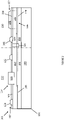
Figure 1 , which includesFigs. 1A, 1B and 1C , illustrates a semiconductor device, according to an embodiment.Fig. 1 illustrates a cross-sectional view of a semiconductor die that comprises a high-electron mobility transistor and a monolithically integrated capacitor.Fig. 1B illustrates a schematic of the high-electron mobility transistor.Fig. 1C illustrates a schematic of the capacitor. -
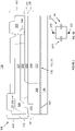
Figure 2 illustrates a cross-sectional view of a semiconductor die that comprises a high-electron mobility transistor and a monolithically integrated capacitor, according to another embodiment. -
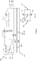
Figure 3 , which includesFigs. 3A and 3B , illustrates a semiconductor device, according to an embodiment.Fig. 3A illustrates a cross-sectional view of a lateral region of a semiconductor die that comprises a monolithically integrated capacitor.Fig. 3B illustrates a schematic of the capacitor. -
Figure 4 , which includesFigs. 4A, 4B , illustrates a semiconductor device, according to an embodiment.Fig. 4A illustrates a cross-sectional view of a lateral region of a semiconductor die that comprises a monolithically integrated capacitor.Fig. 4B illustrates a schematic of the capacitor. - Embodiments of a capacitor that is monolithically integrated in a semiconductor die that comprises type III-V semiconductor material are described herein. The semiconductor die comprises type III-V semiconductor that comprises barrier and channel layers of type III-V semiconductor material. The barrier and channel layers form a heterojunction such that a two-dimensional charge carrier gas arises in the channel layer near the heterojunction. This basic arrangement can be used to form a high-electron mobility transistor in the semiconductor die that utilizes the two-dimensional charge carrier gas as an active device channel. The capacitor utilizes the same basic arrangement of the barrier and channel layers from the semiconductor die to form part of its charge storing structure. Specifically, a dielectric medium of the capacitor corresponds to a lateral section of the barrier layer, and a region of the two-dimensional charge carrier gas underneath the barrier layer corresponds to a first electrode of the capacitor. The second electrode of the capacitor is provided from a structured region of metallization on top of the barrier layer. This capacitor structure can be combined with further capacitor structures formed in superjacent dielectric and metallization layers that are vertically interdigitated with one another. By using the built-in features of the type III-V semiconductor substrate, a monolithically integrated capacitor with greater capacitance per area than previous solutions is produced.
- Referring to
Figure 1 , asemiconductor die 100 comprises asemiconductor substrate 102. Thesemiconductor substrate 102 comprises abarrier layer 104 and achannel layer 106 disposed below thebarrier layer 104. Thebarrier layer 104 comprises type III-V semiconductor material and thechannel layer 106 comprises type III-V semiconductor material with a different bandgap as thebarrier layer 104. For instance, thechannel layer 106 can comprise GaN or AIGaN and thebarrier layer 104 can comprise AIGaN with a higher aluminum content as thechannel layer 106. Thechannel layer 106 forms a heterojunction with thebarrier layer 104 such that a two-dimensionalcharge carrier gas 108 is disposed in thechannel layer 106 near the heterojunction interface. The term two-dimensionalcharge carrier gas 108 refers to a two-dimensional electron gas ("2DEG") or a two-dimensional hole gas ("2DHG"). In the above example wherein thechannel layer 106 is a GaN layer and thebarrier layer 104 is a layer of AIGaN, the two-dimensionalcharge carrier gas 108 is a 2DEG. - The
semiconductor substrate 102 additionally comprises a back-barrier region 109 disposed below thechannel layer 106. The back-barrier region 109 may comprise multiple layers of different semiconductor material that serve different purposes. For instance, the back-barrier region 109 may comprise a base substrate that extends to a rear surface of thesemiconductor substrate 102. This base substrate can be a commercially available semiconductor wafer, e.g., a silicon wafer, SOI, sapphire, SiC, and some other ceramic based substrate, that is used to epitaxially grow type III-V semiconductor material thereon. A plurality of type III-V semiconductor layers may be formed on this base substrate below thechannel layer 106. These type III-V semiconductor layers may have different crystalline properties, e.g., layers of GaN/AIGaN with different aluminum content, that are designed to alleviate mechanical stresses in thesemiconductor substrate 102 resulting from lattice mismatch between the base substrate and the superjacent material. - The semiconductor die 100 further comprises a first
dielectric layer 105 and afirst metallization layer 107, with each layer each being disposed on an upper surface of thebarrier layer 104. Generally speaking, thefirst dielectric layer 105 can comprise any of a variety of electrical insulators, such as SiO2 (silicon dioxide), Si3N4 (silicon nitride), SiONXY (silicon oxynitride), etc., including high-K dielectric materials such as HfO2. A thickness of thefirst dielectric layer 105 can generally be in the range of 50nm - 200nm. Thefirst dielectric layer 105 can be formed by a deposition technique such as chemical vapor deposition (CVD), for example. Generally speaking, thefirst metallization layer 107 can comprise any of a variety of conductive metals such as aluminum, titanium, copper, nickel, tungsten, etc., and any alloys (i.e., Ti/AI/Ti) thereof. Thefirst metallization layer 107 can be formed after forming thefirst dielectric layer 105, e.g., by a metal deposition technique such evaporation, plating, molecular beam epitaxy, sputtering, etc. Thefirst dielectric layer 105 and thefirst metallization layer 107 can be formed into desired geometries using masked structuring techniques such as photolithography and/or etching. - A high-
electron mobility transistor 110 is disposed in a firstlateral region 112 of the semiconductor die 100. The high-electron mobility transistor 110 comprises asource terminal 114, adrain terminal 116, and agate terminal 118. In a commonly known manner, the high-electron mobility transistor 110 is configured to control a conductive connection between the source anddrain terminals gate terminal 118. - The semiconductor die 100 comprises source and drain
electrodes first metallization layer 107. The source and drainelectrodes charge carrier gas 108. To this end, the source and drainelectrodes semiconductor substrate 102 to contact the two-dimensionalcharge carrier gas 108. Alternatively, this electrical connection may be provided by another conductive structure (not shown) formed in thesemiconductor substrate 102. The source and drainelectrodes source terminal 114 and thedrain terminal 116 of the high-electron mobility transistor 110. That is, the source and drainelectrodes semiconductor substrate 102 may comprise further layers of upper-level metallization (not shown) that are structured to comprise external bond pads that are electrically connected to the source and drainelectrodes - The high-
electron mobility transistor 110 additionally comprises agate structure 124. Thegate structure 124 comprises agate electrode 126. Thegate electrode 126 is formed from an electrical conductor such as a metal, e.g., aluminum, titanium, copper, nickel, tungsten, alloys thereof, etc., or a doped semiconductor, e.g., highly doped monocrystalline or polycrystalline semiconductors. Thegate electrode 126 can be a part of thefirst metallization layer 107 or may be formed separately. - The working principle of the high-
electron mobility transistor 110 is as follows. The two-dimensionalcharge carrier gas 108 is the active channel of the device. In an on-state of the device, the source and drainelectrodes charge carrier gas 108. In the off-state of the device, the two-dimensionalcharge carrier gas 108 is locally disrupted so that the source and drainelectrodes gate electrode 126. This influences an electric field beneath the gate, which in turn determines whether the two-dimensionalcharge carrier gas 108 is locally disrupted. As shown, thegate electrode 126 is disposed within a trench formed in thebarrier layer 104. This brings thegate electrode 126 closer to the two-dimensionalcharge carrier gas 108, thereby enabling better on-off control. - The depicted configuration illustrates just one potential device configuration of a high-
electron mobility transistor 110 that can be provided in the firstlateral region 112 of the semiconductor die 100. These potential device configurations may vary with respect to geometry, material type and arrangement of the features, provided that the above-described device concept is obtained. For example, thesemiconductor substrate 102 may comprise additional dielectric layers that are used for different purposes, e.g., passivation layers used to protect the semiconductor material, gate dielectric layers used to provide a thin gate dielectric underneath thegate electrode 126, etc. Additionally, or alternatively, thegate structure 124 may additionally comprise a region of type III-V semiconductor material such as p-type GaN disposed underneath thegate electrode 126 that is configured to generate an electric field that disrupts the two-dimensionalcharge carrier gas 108 at zero gate bias, thereby providing a normally-off device. Additionally, or alternatively, thegate structure 124 may have a different geometry from what is shown and/or may not be disposed within a trench. - A
capacitor 128 is disposed in a secondlateral region 130 of the semiconductor die 100. Thecapacitor 128 comprises first andsecond terminals capacitor 128 is configured to store electrical energy between the first andsecond terminals - The
capacitor 128 is monolithically integrated into the semiconductor die 100. This means that the conductive and dielectric structures that collectively form the charge-storing structure ofcapacitor 128 are formed by constituent components of the semiconductor die 100. These constituent components include layers or regions of type III-V semiconductor material from thesemiconductor substrate 102 and the dielectric layers and/or conductive layers disposed thereon. - The
capacitor 128 comprises a dielectric medium that comprises afirst section 132 of thebarrier layer 104 that is disposed in the secondlateral region 130. As previously discussed, thebarrier layer 104 of thesemiconductor substrate 102 comprises a type III-V semiconductor material such as GaN/AIGaN. The relative dielectric constant of type III-V semiconductor material such as GaN is generally in the range of 9-10 (between 9.2 and 9.5 in the specific case of GaN). The thickness of thebarrier layer 104 can be selected based upon desired capacitor characteristics such as capacitance and maximum voltage. Although type III-V semiconductor materials have a high dielectric constant, they generally have a lower dielectric strength than semiconductor-based oxide or nitride materials, e.g., silicon dioxide, silicon nitride, etc. The dielectric medium of thecapacitor 128 may additionally comprise afirst section 134 of thefirst dielectric layer 105 that is disposed abovefirst section 132 of thebarrier layer 104. As the dielectric strength of the materials used to form the first dielectric layer 105 (e.g., silicon nitride, silicon dioxide) is greater than that of thebarrier layer 104, this configuration enables higher voltage operation (e.g., above 20V, above 50V, above 100V, etc.) without the possibility of dielectric breakdown. Meanwhile, the thickness of thebarrier layer 104 can remain at values that are well-suited for the performance of the high-electron mobility transistor 110, e.g., in the range of 7 nm to 100 nm. - According to an embodiment, the
capacitor 128 is configured as a parallel plate capacitor. A parallel plate capacitor refers to a type of capacitor wherein the electrodes form conductive two-dimensional planes that are parallel to one another and with the dielectric medium interposed between the planar electrode structures. The capacitance of a parallel plate capacitor is determined by the following equation (1):
- C is the capacitance (in farads);
- A is the area of overlap of the electrodes on either side of the dielectric medium;
- k is the relative permittivity of the dielectric medium;
- ε0 is the dielectric permittivity of a vacuum; and
- d is the separation between the plates.
- A first electrode of the
capacitor 128 is provided by aregion 136 of the two-dimensionalcharge carrier gas 108 that is underneath thefirst section 132 of thebarrier layer 104. As the two-dimensionalcharge carrier gas 108 is electrically conductive and expands along a two-dimensional area along the interface betweenbarrier layer 104 and thechannel layer 106, it essentially acts as a "built in" plate for a parallel plate capacitor structure. Thesemiconductor substrate 102 may additionally comprise adielectric structure 138 that laterally isolates the two-dimensionalcharge carrier gas 108 in the secondlateral region 130 from the two-dimensionalcharge carrier gas 108 in the firstlateral region 112. In this way, thecapacitor 128 can operate independently from the high-electron mobility transistor 110. Thedielectric structure 138 can comprise an electrical insulator, e.g., silicon dioxide, silicon nitride, etc., disposed within a trench formed in thesemiconductor substrate 102. More generally, any lateral electrical isolation structure is possible. - A second plate of the
capacitor 128 is provided by afirst section 140 of thefirst metallization layer 107 that is above thefirst section 132 of thebarrier layer 104 and (optionally) thefirst section 134 of thefirst dielectric layer 105. The area of overlap between thefirst section 140 of thefirst metallization layer 107 and the two-dimensionalcharge carrier gas 108 define the area of overlap (A) in the above-provided equation (1). Put another way, thefirst metallization layer 107 is structured in such a way to form a parallel plate electrode, thus completing the capacitor structure using the "built-in" dielectric medium and conductive plate provided by thesemiconductor substrate 102. - A
second section 142 of thefirst metallization layer 107 that is formed in the secondlateral region 130 is in low-ohmic contact with the two-dimensionalcharge carrier gas 108, e.g., in a similar manner as the source and drainelectrodes capacitor 128. The first andsecond terminals capacitor 128 can respectively correspond to the first andsecond sections first metallization layer 107. Alternatively, thesemiconductor substrate 102 may comprise further layers of upper-level metallization (not shown) that are structured to comprise external bond pads that are electrically connected to the first andsecond sections - The first and
second terminals capacitor 128 can be series-connected or parallel-connected with thesource terminal 114, thedrain electrode 116 and/or thegate terminal 118 of the high-electron mobility transistor 110 in any possible arrangement. These electrical connections may be provided by forming interconnections in thefirst metallization layer 107 and/or any metallization layer disposed thereon, for example. - Referring to
Fig. 2 , asemiconductor die 100 is depicted, according to another embodiment. The semiconductor die 100 differs from the embodiment ofFig. 1 in that a damagedregion 141 is provided instead of the dielectric structure. The damagedregion 141 is a portion of thesemiconductor substrate 102 wherein crystalline defects are intentionally created in the material. As a result, the two-dimensionalcharge carrier gas 108 is disrupted such that the two-dimensionalcharge carrier gas 108 in the secondlateral region 130 is isolated from is isolated from the two-dimensionalcharge carrier gas 108 in the firstlateral region 112 in a similar manner as described above. The damagedregion 141 can be created by ion implantation, for example. - Referring to
Fig. 3 , the secondlateral region 130 of thesemiconductor substrate 102 is shown, according to another embodiment. In this embodiment, the monolithically integratedcapacitor 128 comprises first and secondparallel plate capacitors parallel plate capacitor 144 is a parallel plate capacitor formed by the two-dimensionalcharge carrier gas 108, thefirst section 132 of thebarrier layer 104, (optionally), thefirst section 134 of thefirst dielectric layer 105, and thefirst section 140 of thefirst metallization layer 107 according to the configuration described with reference toFig. 1 . The secondparallel plate capacitor 146 is connected in parallel with the firstparallel plate capacitor 144 and therefore adds to the overall capacitance of thecapacitor 128. The secondparallel plate capacitor 146 is vertically stacked on top of the firstparallel plate capacitor 144. This means that the dielectric medium of the secondparallel plate capacitor 146 at least partially overlaps with the dielectric medium of the firstparallel plate capacitor 144. As a result, the overall capacitance of thecapacitor 128 is increased without adding a commensurate amount of additional chip area for the secondparallel plate capacitor 146. - The
semiconductor substrate 102 comprises asecond dielectric layer 148 and asecond metallization layer 150 that are each disposed over an upper surface of thebarrier layer 104. Thesecond dielectric layer 148 is formed after forming thefirst metallization layer 107. Thesecond metallization layer 150 is formed after forming thesecond dielectric layer 148. Thesecond metallization layer 150 and thesecond dielectric layer 148 can have the same material composition and can be formed according to the same techniques as thefirst metallization layer 107 and thefirst dielectric layer 105, respectively. - The dielectric medium of the second
parallel plate capacitor 146 corresponds to afirst section 152 of thesecond dielectric layer 148 that is above thefirst metallization layer 107. A first electrode of the secondparallel plate capacitor 146 corresponds to afirst section 154 of thesecond metallization layer 150 that is above thefirst section 152 of thesecond dielectric layer 148. The first electrode of the secondparallel plate capacitor 146 is electrically connected to the first electrode of the firstparallel plate capacitor 144, both of which connect with thesecond terminal 131 of the capacitor. As shown inFigure 2 , this electrical connection can be effectuated by asecond section 156 of thesecond metallization layer 150 which contacts thesecond section 142 of thefirst metallization layer 150. Meanwhile, the second conductive plate of the secondparallel plate capacitor 146 comprises thefirst section 140 of thefirst metallization layer 107. - That is, the same structure which forms the second conductive plate of the first
parallel plate capacitor 144 also forms at least part of the second conductive plate of the secondparallel plate capacitor 146. - The semiconductor die 100 further comprises a third
dielectric layer 158 and athird metallization layer 160 that are each disposed over the upper surface of thebarrier layer 104. The thirddielectric layer 158 is formed after forming thesecond metallization layer 150. Thethird metallization layer 160 is formed after forming thesecond dielectric layer 148. Thethird metallization layer 160 and the thirddielectric layer 158 can have the same material composition and can be formed according to the same techniques as thefirst metallization layer 107 and thefirst dielectric layer 105, respectively. - In the embodiment of
Fig. 3 , thethird metallization layer 160 is structured to form externally accessible contact structures (bond pads) which correspond to the first andsecond terminals capacitor 128. The thirddielectric layer 158 provides an outermost surface of the semiconductor die 100 in between these contact structures which protects the device from contamination. - Referring to
Fig. 4 , the secondlateral region 130 of the semiconductor die 100 is shown, according to another embodiment. In this embodiment, the monolithically integratedcapacitor 128 comprises first, second and thirdparallel plate capacitors parallel plate capacitors Fig. 3 . The thirdparallel plate capacitor 162 that is connected in parallel with the first and secondparallel plate capacitors parallel plate capacitors capacitor 128 is increased without adding commensurate amount of additional chip area for the thirdparallel plate capacitor 162. - The third
parallel plate capacitor 162 is obtained through structuring of thethird metallization layer 160 to form an additional parallel plate electrode. Specifically, thethird metallization layer 160 is structured so that afirst section 162 of the thirddielectric layer 158 is covered by afirst section 164 of thethird metallization layer 164. Thefirst section 162 of the thirddielectric layer 158 forms the dielectric medium of the thirdparallel plate capacitor 162. Thefirst section 164 of thethird metallization layer 164 forms a second conductive plate of the thirdparallel plate capacitor 162 that is electrically connected to the second conductive plates of the first and second parallel plate capacitors by direct contact with thefirst metallization layer 107. Meanwhile, the second conductive plate of the thirdparallel plate capacitor 162 comprises thefirst section 154 of thesecond metallization layer 150. That is, the same structure which forms the first conductive plate of the secondparallel plate capacitor 146 also forms at least part of the first conductive plate of the thirdparallel plate capacitor 162. - The vertical stacking concept illustrated by the embodiments of
Figs. 2 and3 can be used to further increase the capacitance of thecapacitor 128 by correspondingly adding and structuring metallization and dielectric. That is, the semiconductor die 100 can be formed to comprise further layers of metallization and dielectric material that are arranged alternatively and structured to form further plate structures. As a result, a monolithically integratedcapacitor 128 that consists of four, five, six, etc.parallel plate capacitors 128 can be obtained. In addition or in the alternative, the semiconductor die 100 can be configured to comprise two or more isolated capacitor structures by incorporating thecapacitor 128 disclosed herein in two or more laterally isolated regions of the semiconductor die 100. - The semiconductor die 100 described herein can comprise a
semiconductor substrate 102 comprising any combination of type III-V semiconductor materials capable of forming a two-dimensional charge carrier gas at a heterojunction between type III-V semiconductor materials of different bandgap. These type III-V semiconductor materials include binary III-V semiconductor materials such as Gallium nitride (GaN), gallium arsenide (GaAs), aluminium nitride (AIN), aluminium arsenide (AlAs), indium nitride (InN), indium arsenide (InAs), etc., and ternary or quarternary type III-V semiconductor materials such as aluminium gallium nitride (AIGaN), aluminium gallium arsenide (AIGaAs), indium gallium nitride (InGaN), indium aluminium gallium nitride (InAIGaN), etc. - As used herein, the phrase "type III-V semiconductor material" refers to a compound material that includes at least one Group III element, such as aluminum (Al), gallium (Ga), indium (In), and boron (B) and at least one Group IV element, such as nitrogen (N), phosphorous (P), and arsenic (As), and including but not limited to any of its alloys, such as aluminum gallium nitride (AlxGa(1-x)N), indium gallium nitride (InyGa(1-y)N), aluminum indium gallium nitride (AlxInyGa(1-x-y)N), gallium arsenide phosphide nitride (GaAsaPbN(1-a-b)), and aluminum indium gallium arsenide phosphide nitride (AlxInyGa(1-x-y)AsaPbN(1-a-b)), for example. Aluminum gallium nitride and AIGaN refers to an alloy described by the formula AlxGa(1-x)N, where 0 < x < 1.
- Spatially relative terms such as "under," "below," "lower," "over," "upper" and the like, are used for ease of description to explain the positioning of one element relative to a second element. These terms are intended to encompass different orientations of the device in addition to different orientations than those depicted in the figures. Further, terms such as "first," "second," and the like, are also used to describe various elements, regions, sections, etc. and are also not intended to be limiting. Like terms refer to like elements throughout the description.
- As used herein, the terms "having," "containing," "including," "comprising" and the like are open-ended terms that indicate the presence of stated elements or features, but do not preclude additional elements or features. The articles "a," "an" and "the" are intended to include the plural as well as the singular, unless the context clearly indicates otherwise.
- With the above range of variations and applications in mind, it should be understood that the present invention is not limited by the foregoing description, nor is it limited by the accompanying drawings. Instead, the present invention is limited only by the following claims and their legal equivalents.
Claims (15)
- A semiconductor device, comprising:a semiconductor die (100) comprising a barrier layer (104) of type III-V semiconductor material, a channel layer (106) of type III-V semiconductor material disposed below the barrier layer (104), the channel layer (106) forming a heterojunction with the barrier layer (104) such that a two-dimensional charge carrier gas (108) is disposed in the channel layer near the heterojunction;a high-electron mobility transistor (110) disposed in a first lateral region (112) of the semiconductor die (100), the high-electron mobility transistor (110) comprising source and drain electrodes (120, 122) that each are in ohmic contact with the two-dimensional charge carrier gas (108) and a gate structure (124) that is configured to control a conductive connection between the source and drain electrodes (120, 122); anda capacitor (128) that is monolithically integrated into the semiconductor die (100) and is disposed in a second lateral region (130) of the semiconductor die (100),wherein a dielectric medium of the capacitor (128) comprises a first section (132) of the barrier layer (104).
- The semiconductor device of claim 1, wherein the capacitor (128) comprises a first parallel plate capacitor connected between first and second terminals (129, 131) of the capacitor (128), and wherein a region (136) of the two-dimensional charge carrier gas (108) that is underneath the first section (132) of the barrier layer (104) forms a first electrode of the first parallel plate capacitor.
- The semiconductor device of claim 2, wherein the semiconductor die (100) comprises a first metallization layer (107) disposed over the barrier layer (104), and wherein a first section (140) of the first metallization layer (107) that is above the first section (132) of the barrier layer (104) forms a second electrode of the first parallel plate capacitor.
- The semiconductor device of claim 3, wherein the semiconductor die (100) comprises a first dielectric layer (105) disposed over the barrier layer (104), and wherein the dielectric medium of the first parallel plate capacitor further comprises a first section (134) of the first dielectric layer (105) that is disposed on top of the first section (136) of the barrier layer (104).
- The semiconductor device of claim 4, wherein the first dielectric layer (105) comprises any one or more of: silicon dioxide, silicon nitride, and silicon oxynitride.
- The semiconductor device of claim 3 or claim 4, wherein the source and drain electrodes (120, 122) of the high-electron mobility transistor (110) are each formed in the first metallization layer (107).
- The semiconductor device of claim 3, wherein the capacitor (128) further comprises a second parallel plate capacitor (146) connected between the first and second terminals (129, 131) in parallel with the first parallel plate capacitor (144).
- The semiconductor device of claim 7, wherein the second parallel plate (146) capacitor is vertically stacked on top of the first parallel plate capacitor (144).
- The semiconductor device of claim 7 or claim 8, wherein the semiconductor die (100) further comprises a second dielectric layer (148) and a second metallization layer (150) that are each disposed over the barrier layer (104), and wherein a dielectric medium of the second parallel plate capacitor (146) comprises a first section (152) of the second dielectric layer (148) that is above the first metallization layer (107).
- The semiconductor device of claim 9, wherein a first section (154) of the second metallization layer (150) that is above the first section (152) of the second dielectric layer (148) forms a first electrode of the second parallel plate capacitor (146), and wherein a second electrode of the second parallel plate capacitor (146) comprises the first section (140) of the first metallization layer (107).
- The semiconductor device of claim 9, further comprising a third parallel plate capacitor (162) connected in parallel with the first and second parallel plate capacitors (144, 146).
- The semiconductor device of claim 11, wherein the semiconductor die (100) comprises a third dielectric layer (158) and a third metallization layer (160) that are each disposed over the barrier layer (104), and wherein a dielectric medium of the third parallel plate capacitor (162) comprises a first section (162) of the third dielectric layer (158) that is above the second metallization layer (150).
- The semiconductor device of claim 12, wherein a first section (164) of the third metallization layer (160) that is above the first section (162) of the third dielectric layer (158) forms a second electrode of the third parallel plate capacitor (162), and wherein a first electrode of the third parallel plate capacitor (162) comprises the first section (154) of the second metallization layer (150).
- The semiconductor device of any one of claims 1 to 13, wherein the channel layer (106) comprises GaN and the barrier layer (104) comprises AIGaN.
- A semiconductor device, comprising:a semiconductor die (100) comprising a barrier layer (104) of type III-V semiconductor material, a channel layer (106) of type III-V semiconductor material disposed below the barrier layer (104), the channel layer (106) forming a heterojunction with the barrier layer (104) such that a two-dimensional charge carrier gas (108) is disposed in the channel layer (106) near the heterojunction; anda capacitor (128) monolithically formed in the semiconductor die (100),wherein a dielectric medium of the capacitor (128) comprises a first section (132) of the barrier layer (104).
Applications Claiming Priority (1)
| Application Number | Priority Date | Filing Date | Title |
|---|---|---|---|
| US17/196,258 US11545485B2 (en) | 2021-03-09 | 2021-03-09 | Type III-V semiconductor substrate with monolithically integrated capacitor |
Publications (2)
| Publication Number | Publication Date |
|---|---|
| EP4057347A2 true EP4057347A2 (en) | 2022-09-14 |
| EP4057347A3 EP4057347A3 (en) | 2022-11-30 |
Family
ID=80461016
Family Applications (1)
| Application Number | Title | Priority Date | Filing Date |
|---|---|---|---|
| EP22158907.0A Pending EP4057347A3 (en) | 2021-03-09 | 2022-02-25 | Type iii-v semiconductor substrate with monolithically integrated capacitor |
Country Status (3)
| Country | Link |
|---|---|
| US (2) | US11545485B2 (en) |
| EP (1) | EP4057347A3 (en) |
| CN (1) | CN115050738A (en) |
Cited By (2)
| Publication number | Priority date | Publication date | Assignee | Title |
|---|---|---|---|---|
| US20230049654A1 (en) * | 2021-03-09 | 2023-02-16 | Infineon Technologies Austria Ag | Type III-V Semiconductor Substrate with Monolithically Integrated Capacitor |
| EP4495990A1 (en) * | 2023-07-19 | 2025-01-22 | Infineon Technologies Austria AG | Semiconductor substrate, semiconductor component and methods |
Families Citing this family (3)
| Publication number | Priority date | Publication date | Assignee | Title |
|---|---|---|---|---|
| US11901402B2 (en) * | 2021-11-18 | 2024-02-13 | Texas Instruments Incorporated | Standalone isolation capacitor |
| CN115440674B (en) * | 2022-09-23 | 2023-11-17 | 上海新微半导体有限公司 | HEMT device and capacitor integrated structure, integration method thereof and power amplifier |
| CN116487446B (en) * | 2023-06-20 | 2024-06-18 | 南方科技大学 | Capacitor, method of manufacturing the same, and method of using the same |
Family Cites Families (30)
| Publication number | Priority date | Publication date | Assignee | Title |
|---|---|---|---|---|
| CN101414633B (en) * | 2008-12-01 | 2010-04-21 | 西安电子科技大学 | High Electron Mobility Device with Groove Insulated Gate Composite Gate Field Plate |
| KR101919422B1 (en) | 2012-09-28 | 2019-02-08 | 삼성전자주식회사 | Nitride semiconductor based power converting device |
| US9379050B2 (en) * | 2013-02-28 | 2016-06-28 | Infineon Technologies Austria Ag | Electronic device |
| JP2015233098A (en) * | 2014-06-10 | 2015-12-24 | 株式会社東芝 | Semiconductor device and method for manufacturing the same |
| JP6395502B2 (en) * | 2014-08-20 | 2018-09-26 | ルネサスエレクトロニクス株式会社 | Semiconductor device |
| US9960154B2 (en) | 2014-09-19 | 2018-05-01 | Navitas Semiconductor, Inc. | GaN structures |
| TWI563631B (en) | 2015-07-21 | 2016-12-21 | Delta Electronics Inc | Semiconductor Device |
| US11289593B2 (en) * | 2015-07-31 | 2022-03-29 | Infineon Technologies Austria Ag | Breakdown resistant HEMT substrate and device |
| US9570438B1 (en) * | 2015-08-04 | 2017-02-14 | Infineon Technologies Austria Ag | Avalanche-rugged quasi-vertical HEMT |
| US10932684B2 (en) * | 2016-03-10 | 2021-03-02 | Epitronic Holdings Pte Ltd. | Microelectronic sensor for air quality monitoring |
| WO2017199110A1 (en) * | 2016-05-17 | 2017-11-23 | Rg Innovations Pte Ltd | Microelectronic sensor for biometric authentication |
| TWI706566B (en) * | 2016-08-01 | 2020-10-01 | 晶元光電股份有限公司 | A high power semiconductor device |
| US9881862B1 (en) * | 2016-09-20 | 2018-01-30 | Infineon Technologies Austria Ag | Top side cooling for GaN power device |
| US11588024B2 (en) * | 2017-03-17 | 2023-02-21 | Infineon Technologies Austria Ag | High voltage blocking III-V semiconductor device |
| US10128228B1 (en) * | 2017-06-22 | 2018-11-13 | Infineon Technologies Americas Corp. | Type III-V semiconductor device with integrated diode |
| US10224924B1 (en) * | 2017-08-22 | 2019-03-05 | Infineon Technologies Austria Ag | Bidirectional switch with passive electrical network for substrate potential stabilization |
| US10332876B2 (en) * | 2017-09-14 | 2019-06-25 | Infineon Technologies Austria Ag | Method of forming compound semiconductor body |
| US10644142B2 (en) * | 2017-12-22 | 2020-05-05 | Nxp Usa, Inc. | Semiconductor devices with doped regions functioning as enhanced resistivity regions or diffusion barriers, and methods of fabrication therefor |
| US10516023B2 (en) * | 2018-03-06 | 2019-12-24 | Infineon Technologies Austria Ag | High electron mobility transistor with deep charge carrier gas contact structure |
| US10541313B2 (en) * | 2018-03-06 | 2020-01-21 | Infineon Technologies Austria Ag | High Electron Mobility Transistor with dual thickness barrier layer |
| US10680069B2 (en) * | 2018-08-03 | 2020-06-09 | Infineon Technologies Austria Ag | System and method for a GaN-based start-up circuit |
| US10770455B2 (en) * | 2018-09-25 | 2020-09-08 | Semiconductor Components Industries, Llc | Electronic device including a transistor and a variable capacitor |
| US20200303534A1 (en) * | 2019-03-21 | 2020-09-24 | Epitronic Holdings Pte. Ltd. | Microelectronic sensor with an aharonov-bohm antenna |
| WO2020188342A1 (en) * | 2019-03-21 | 2020-09-24 | Epitronic Holdings Pte. Ltd. | Microelectronic device for electronic sorbent assay and for monitoring biological cell dynamics comprising pseudo-conductive high-electron mobility transistor (hemt) |
| US11081455B2 (en) * | 2019-04-29 | 2021-08-03 | Infineon Technologies Austria Ag | Semiconductor device with bond pad extensions formed on molded appendage |
| US10720913B1 (en) * | 2019-05-28 | 2020-07-21 | Infineon Technologies Austria Ag | Integrated failsafe pulldown circuit for GaN switch |
| US12015062B2 (en) * | 2019-10-24 | 2024-06-18 | Fraunhofer-Gesellschaft zur Förderung der angewandten Forschung e.V. | Integrated circuit |
| EP3905523B1 (en) * | 2020-04-30 | 2024-06-19 | Infineon Technologies Austria AG | Switching circuit, gate driver and method of operating a transistor device |
| US11521907B2 (en) * | 2020-10-14 | 2022-12-06 | Infineon Technologies Ag | Hybrid embedded package |
| US11545485B2 (en) * | 2021-03-09 | 2023-01-03 | Infineon Technologies Austria Ag | Type III-V semiconductor substrate with monolithically integrated capacitor |
-
2021
- 2021-03-09 US US17/196,258 patent/US11545485B2/en active Active
-
2022
- 2022-02-25 EP EP22158907.0A patent/EP4057347A3/en active Pending
- 2022-03-09 CN CN202210222693.3A patent/CN115050738A/en active Pending
- 2022-10-31 US US17/977,875 patent/US11916068B2/en active Active
Cited By (3)
| Publication number | Priority date | Publication date | Assignee | Title |
|---|---|---|---|---|
| US20230049654A1 (en) * | 2021-03-09 | 2023-02-16 | Infineon Technologies Austria Ag | Type III-V Semiconductor Substrate with Monolithically Integrated Capacitor |
| US11916068B2 (en) * | 2021-03-09 | 2024-02-27 | Infineon Technologies Austria Ag | Type III-V semiconductor substrate with monolithically integrated capacitor |
| EP4495990A1 (en) * | 2023-07-19 | 2025-01-22 | Infineon Technologies Austria AG | Semiconductor substrate, semiconductor component and methods |
Also Published As
| Publication number | Publication date |
|---|---|
| US11545485B2 (en) | 2023-01-03 |
| US11916068B2 (en) | 2024-02-27 |
| US20220293589A1 (en) | 2022-09-15 |
| US20230049654A1 (en) | 2023-02-16 |
| EP4057347A3 (en) | 2022-11-30 |
| CN115050738A (en) | 2022-09-13 |
Similar Documents
| Publication | Publication Date | Title |
|---|---|---|
| US11916068B2 (en) | Type III-V semiconductor substrate with monolithically integrated capacitor | |
| US10332876B2 (en) | Method of forming compound semiconductor body | |
| US9142550B2 (en) | High-voltage cascaded diode with HEMT and monolithically integrated semiconductor diode | |
| US11594628B2 (en) | Monolithic microwave integrated circuits having both enhancement-mode and depletion mode transistors | |
| US10134850B2 (en) | Semiconductor device | |
| CN110010562B (en) | Semiconductor device | |
| US9748242B2 (en) | Semiconductor device | |
| US20200395474A1 (en) | High electron mobility transistors having improved contact spacing and/or improved contact vias | |
| US12205945B2 (en) | Semiconductor device and manufacturing method thereof | |
| US9564524B2 (en) | Semiconductor device and method | |
| US20240178285A1 (en) | High electron mobility transistor and fabrication method thereof | |
| US20220130987A1 (en) | High Voltage Blocking III-V Semiconductor Device | |
| US12635169B2 (en) | Semiconductor device integrating a high electron mobility transistor and a resistor | |
| US12218202B2 (en) | Semiconductor device incorporating a substrate recess | |
| US12513981B2 (en) | Semiconductor device | |
| TWI839007B (en) | Semiconductor device | |
| EP4428927B1 (en) | Multi-channel high electron mobility transistor with reduced input capacitance | |
| US20250015076A1 (en) | Semiconductor die with group iii nitride-based amplifier circuits | |
| US20250167116A1 (en) | Group iii nitride transistor device and method for fabricating a group iii nitride transistor device | |
| JP2026079430A (en) | Semiconductor equipment | |
| CN118198006A (en) | Semiconductor devices |
Legal Events
| Date | Code | Title | Description |
|---|---|---|---|
| PUAI | Public reference made under article 153(3) epc to a published international application that has entered the european phase |
Free format text: ORIGINAL CODE: 0009012 |
|
| STAA | Information on the status of an ep patent application or granted ep patent |
Free format text: STATUS: THE APPLICATION HAS BEEN PUBLISHED |
|
| AK | Designated contracting states |
Kind code of ref document: A2 Designated state(s): AL AT BE BG CH CY CZ DE DK EE ES FI FR GB GR HR HU IE IS IT LI LT LU LV MC MK MT NL NO PL PT RO RS SE SI SK SM TR |
|
| PUAL | Search report despatched |
Free format text: ORIGINAL CODE: 0009013 |
|
| AK | Designated contracting states |
Kind code of ref document: A3 Designated state(s): AL AT BE BG CH CY CZ DE DK EE ES FI FR GB GR HR HU IE IS IT LI LT LU LV MC MK MT NL NO PL PT RO RS SE SI SK SM TR |
|
| RIC1 | Information provided on ipc code assigned before grant |
Ipc: H01L 29/778 20060101ALI20221024BHEP Ipc: H01L 49/02 20060101ALI20221024BHEP Ipc: H01L 27/06 20060101AFI20221024BHEP |
|
| STAA | Information on the status of an ep patent application or granted ep patent |
Free format text: STATUS: REQUEST FOR EXAMINATION WAS MADE |
|
| 17P | Request for examination filed |
Effective date: 20230530 |
|
| RBV | Designated contracting states (corrected) |
Designated state(s): AL AT BE BG CH CY CZ DE DK EE ES FI FR GB GR HR HU IE IS IT LI LT LU LV MC MK MT NL NO PL PT RO RS SE SI SK SM TR |