EP4057313A1 - Integrated electronic switch and power tool - Google Patents
Integrated electronic switch and power tool Download PDFInfo
- Publication number
- EP4057313A1 EP4057313A1 EP22161225.2A EP22161225A EP4057313A1 EP 4057313 A1 EP4057313 A1 EP 4057313A1 EP 22161225 A EP22161225 A EP 22161225A EP 4057313 A1 EP4057313 A1 EP 4057313A1
- Authority
- EP
- European Patent Office
- Prior art keywords
- electronic switch
- integrated electronic
- circuit board
- disposed
- switching elements
- Prior art date
- Legal status (The legal status is an assumption and is not a legal conclusion. Google has not performed a legal analysis and makes no representation as to the accuracy of the status listed.)
- Granted
Links
Images




Classifications
-
- H—ELECTRICITY
- H01—ELECTRIC ELEMENTS
- H01H—ELECTRIC SWITCHES; RELAYS; SELECTORS; EMERGENCY PROTECTIVE DEVICES
- H01H13/00—Switches having rectilinearly-movable operating part or parts adapted for pushing or pulling in one direction only, e.g. push-button switch
- H01H13/02—Details
- H01H13/04—Cases; Covers
- H01H13/08—Casing of switch constituted by a handle serving a purpose other than the actuation of the switch
-
- H—ELECTRICITY
- H01—ELECTRIC ELEMENTS
- H01H—ELECTRIC SWITCHES; RELAYS; SELECTORS; EMERGENCY PROTECTIVE DEVICES
- H01H13/00—Switches having rectilinearly-movable operating part or parts adapted for pushing or pulling in one direction only, e.g. push-button switch
- H01H13/02—Details
- H01H13/12—Movable parts; Contacts mounted thereon
- H01H13/14—Operating parts, e.g. push-button
-
- B—PERFORMING OPERATIONS; TRANSPORTING
- B25—HAND TOOLS; PORTABLE POWER-DRIVEN TOOLS; MANIPULATORS
- B25F—COMBINATION OR MULTI-PURPOSE TOOLS NOT OTHERWISE PROVIDED FOR; DETAILS OR COMPONENTS OF PORTABLE POWER-DRIVEN TOOLS NOT PARTICULARLY RELATED TO THE OPERATIONS PERFORMED AND NOT OTHERWISE PROVIDED FOR
- B25F5/00—Details or components of portable power-driven tools not particularly related to the operations performed and not otherwise provided for
- B25F5/001—Gearings, speed selectors, clutches or the like specially adapted for rotary tools
-
- H—ELECTRICITY
- H01—ELECTRIC ELEMENTS
- H01H—ELECTRIC SWITCHES; RELAYS; SELECTORS; EMERGENCY PROTECTIVE DEVICES
- H01H9/00—Details of switching devices, not covered by groups H01H1/00 - H01H7/00
- H01H9/52—Cooling of switch parts
-
- H—ELECTRICITY
- H02—GENERATION; CONVERSION OR DISTRIBUTION OF ELECTRIC POWER
- H02K—DYNAMO-ELECTRIC MACHINES
- H02K7/00—Arrangements for handling mechanical energy structurally associated with dynamo-electric machines, e.g. structural association with mechanical driving motors or auxiliary dynamo-electric machines
- H02K7/14—Structural association with mechanical loads, e.g. with hand-held machine tools or fans
- H02K7/145—Hand-held machine tool
-
- H—ELECTRICITY
- H05—ELECTRIC TECHNIQUES NOT OTHERWISE PROVIDED FOR
- H05K—PRINTED CIRCUITS; CASINGS OR CONSTRUCTIONAL DETAILS OF ELECTRIC APPARATUS; MANUFACTURE OF ASSEMBLAGES OF ELECTRICAL COMPONENTS
- H05K1/00—Printed circuits
- H05K1/18—Printed circuits structurally associated with non-printed electric components
- H05K1/181—Printed circuits structurally associated with non-printed electric components associated with surface mounted components
-
- H—ELECTRICITY
- H01—ELECTRIC ELEMENTS
- H01H—ELECTRIC SWITCHES; RELAYS; SELECTORS; EMERGENCY PROTECTIVE DEVICES
- H01H9/00—Details of switching devices, not covered by groups H01H1/00 - H01H7/00
- H01H9/02—Bases, casings, or covers
- H01H9/06—Casing of switch constituted by a handle serving a purpose other than the actuation of the switch, e.g. by the handle of a vacuum cleaner
- H01H2009/065—Battery operated hand tools in which the battery and the switch are directly connected
-
- H—ELECTRICITY
- H05—ELECTRIC TECHNIQUES NOT OTHERWISE PROVIDED FOR
- H05K—PRINTED CIRCUITS; CASINGS OR CONSTRUCTIONAL DETAILS OF ELECTRIC APPARATUS; MANUFACTURE OF ASSEMBLAGES OF ELECTRICAL COMPONENTS
- H05K2201/00—Indexing scheme relating to printed circuits covered by H05K1/00
- H05K2201/10—Details of components or other objects attached to or integrated in a printed circuit board
- H05K2201/10007—Types of components
- H05K2201/10053—Switch
Definitions
- the present disclosure relates to an integrated electronic switch and, in particular, to an integrated electronic switch of a hand-held power tool.
- the present disclosure provides an integrated electronic switch, which integrates a control circuit and a power switch circuit on a same PCB board, solves the heat dissipation problem of electron components on the PCB board and simultaneously reduces the assembly difficulty of the integrated electronic switch on the basis of miniaturization of the integrated electronic switch.
- the present disclosure provides the following technical solutions.
- the integrated electronic switch includes an input unit and a circuit board.
- the input unit is configured to receive a drive signal output by a user; a sensing module for sensing the drive signal transmitted from the input unit, and a control module electrically connected to the sensing module are disposed on the circuit board, where the sensing module and the control module are disposed on a first side surface of the circuit board.
- the circuit board is provided with multiple switching elements, where the multiple switching elements are electrically connected to the control module.
- the multiple switching elements are disposed on a second side surface of the circuit board.
- the integrated electronic switch also includes a heat dissipation element disposed on the second side surface of the circuit board.
- a heat conduction element configured to transmit heat generated on the multiple switching elements to the heat dissipation element is disposed between the heat dissipation element and the multiple switching elements.
- the input unit includes a trigger and a sensing actuator, and the sensing actuator is provided with at least a power-on sliding blade and a speed-regulating sliding blade.
- the sensing module is formed with a power-on sensing area and a speed-regulating sensing area; and when the integrated electronic switch works, the power-on sensing area is electrically connected to the power-on sliding blade, and the speed-regulating sensing area is electrically connected to the speed-regulating sliding blade.
- the integrated electronic switch also includes a housing formed with accommodation space and the circuit board is at least partially located in the accommodation space.
- the sensing module is disposed in the accommodation space, and the control module is disposed outside the accommodation space.
- the integrated electronic switch includes a housing, a input unit and a circuit board.
- the housing is formed with an accommodation space; an input unit configured to receive a drive signal output by a user.
- the circuit board is at least partially disposed in the accommodation space, and is further provided with multiple switching elements, and a sensing module for sensing the drive signal transmitted from the input unit, where the sensing module is disposed on a first side surface of the circuit board; and the multiple switching elements are disposed on a second side surface of the circuit board.
- the circuit board includes at least a first potion and a second potion, where the first potion is located in the accommodation space, and the second potion is located outside the accommodation space and extends in a front-rear direction.
- the sensing module is disposed on a first side surface of the circuit board; and the multiple switching elements are disposed on a second side surface of the circuit board.
- the integrated electronic switch also includes a heat dissipation element disposed on the second side surface of the circuit board, and the heat dissipation element is fixedly mounted to the second potion of the circuit board.
- the heat dissipation element and the multiple switching elements are disposed opposite to each other in a height direction; and a heat conduction element is disposed between the heat dissipation element and the multiple switching elements and is configured to transmit heat generated on the multiple switching elements to the heat dissipation element.
- the integrated electronic switch also includes a control module electrically connected to the sensing module; and the control module is disposed on the first side surface of the circuit board.
- the input unit includes a trigger and a sensing actuator, and the sensing actuator is provided with at least a power-on sliding blade and a speed-regulating sliding blade.
- the sensing module is formed with an power-on sensing area and a speed-regulating sensing area; and when the integrated electronic switch works, the power-on sensing area is electrically connected to the power-on sliding blade, and the speed-regulating sensing area is electrically connected to the speed-regulating sliding blade.
- the drill 100 includes a tool housing, a motor 20, a fan 30, a gearbox 40 and an output portion 50.
- the tool housing is formed with one handle 11 for a user to hold.
- One end of the handle 11 is connected to a power interface for accessing a direct current (DC) power supply or an alternating current (AC) power supply.
- the power interface is connected to a battery pack 200 which is detachably connected to the drill 100.
- the power port can also be accessed to the alternating current, such as the commercial power.
- An accommodation space (not shown in the figure) is formed in the tool housing along a first straight line 101, and the motor 20, the fan 30, and the gearbox 40 are sequentially disposed in the accommodation space.
- the drill 100 also includes an integrated electronic switch 60 for at least starting the operation of the motor 20 and adjusting a rotational speed of the motor 20.
- FIG. 2 to 5 illustrate an integrated electronic switch 60 as a first embodiment in the present disclosure.
- the integrated electronic switch 60 includes an input unit 61, a housing 62, and a circuit board 63 located within the housing 62.
- the housing 62 includes a sealed accommodation space 623 formed by an upper housing 621 and a lower housing 622.
- the circuit board 63 is disposed in the accommodation space 623.
- the input unit 61 includes a trigger 611 and a sensing actuator 612.
- the sensing actuator 612 is provided with a power-on sliding blade 6121 and a speed-regulating sliding blade 6122.
- the user inputs a drive signal through the trigger 611.
- the drive signal includes a power signal and a speed-regulating signal, and the sensing actuator 612 and the trigger 611 are mechanically connected for transmitting the drive signal inputted by the user.
- the circuit board 63 is provided with a sensing module 631, a control module 632, and multiple switching elements 633.
- the control module 632 is electrically connected to the sensing module 631 and the multiple switching elements 633.
- the sensing module 631 is configured to sense the drive signal output by the input unit 61.
- the sensing module 631 includes an power-on sensing area 6311 and a speed-regulating sensing area 6312.
- the sensing actuator 612 drives the power-on sliding blade 6121 to slide in the power-on sensing area 6311 under the action of the trigger 611, and the speed-regulating sliding blade 6122 to slide in the speed-regulating sensing area 6312, and outputs an analog signal corresponding to the drive signal to the control module 632.
- the speed-regulating sensing area 6312 is provided with a signal output port a2 for outputting an analog signal corresponding to a speed-regulating signal input by the user
- the control module 632 is provided with one signal input port a1 for receiving the analog signal output from a signal output port a2.ln some embodiments, as shown in FIG.
- the signal input port a1 and the signal output port a2 are electrically connected through a jumper 634.
- a resistance may be connected in series between the signal input port a1 and the signal output port a2 for electrical connection through wiring on the circuit board.
- the circuit board 63 has a first side surface 6351 and a second side surface 6352.
- the sensing module 631, the control module 632 and multiple switching elements 633 are disposed on a same side surface of the circuit board 635. Specifically, the sensing module 631, the control module 632 and multiple switching elements 633 are disposed on the first side surface 6351 of the circuit board 63. In other embodiments, the sensing module 631 and the control module 632 are disposed on a same side surface of the circuit board 63. Specifically, the sensing module 631 and the control module 632 are disposed on the first side surface 6351 of the circuit board 63.
- the multiple switching elements 633 are disposed on the second side surface 6352 of the circuit board 63.
- the integrated electronic switch 60 further includes a heat dissipation element 64 for heat dissipation of the circuit board 63.
- the heat dissipation element 64 is at least partially disposed outside the accommodation space 623.
- the upper housing 621 is formed with a mounting groove (not shown in the figure) disposed opposite to the multiple switching elements 633 in an up-down direction.
- the heat dissipation element 64 is embedded in the mounting groove.
- the heat dissipation element 64 is configured to be a metal material having a good thermal conductivity. In other embodiments, referring to FIG.
- the heat dissipation element 64 is integrally formed with the upper housing 621.lt can be understood that when the heat dissipation element 64 is integrally formed with the upper housing 621 in this embodiment, the upper housing 621 is preferably made of the metal material having a good thermal conductivity. Especially, other materials having a good thermal conductivity or a heat absorption property may also be used by those skilled in the art to fabricate the housing, which is not limited in the present disclosure.
- the integrated electronic switch 60 further includes a metal housing 65 disposed on the housing 62.
- the metal housing 65 is fixed to an outer surface of an upper housing 621 and directly or indirectly contacts with the heat dissipation element 64 on the upper housing 621 to derive heat from the heat dissipation element 64.
- the metal housing 65 is secured and mounted to the housing 62 by screws.
- the metal housing 65 is further formed with a hollow grid-shaped heat dissipation area 651 so as to quickly transmit heat generated in the accommodation space 623 of the integrated electronic switch 60 to the outside of the accommodation space 623.
- the integrated electronic switch 60 further includes a reverse diode 66 for providing a return path for a counter-electromotive force generated by the motor 20 when the integrated electronic switch 60 is started/stopped, preventing the counter-electromotive force generated by the motor 20 from returning to the battery pack 200.
- the reverse diode 66 is provided outside the housing 62 of the integrated electronic switch 60, a negative electrode of the reverse diode 66 is electrically connected to a positive electrode of a power input terminal, and a positive electrode of the reverse diode 66 is electrically connected to a negative electrode of the power input terminal.
- the reverse diode 66 may also be disposed on the circuit board 63 of the integrated electronic switch 60.
- FIGS. 7 to 8 illustrate an integrated electronic switch 70 as a second embodiment in the present disclosure.
- the integrated electronic switch 70 includes an input unit 71, a housing 72, and a circuit board 73 located within the housing 72.
- the housing 72 includes a sealed accommodation space 723 formed by an upper housing 721 and a lower housing 722.
- the circuit board 73 is disposed in the accommodation space 723.
- the input unit 71 includes a trigger 711 and a sensing actuator (not shown in the figure).
- the difference from the first embodiment described above lies in that the heat dissipation element 74 includes a first heat dissipation portion (not shown in the figure) located within the accommodation space 723 and a second heat dissipation portion 741 located outside the accommodation space 723.
- the first heat dissipation portion is arranged opposite to the multiple switching elements (not shown in the figure) in an up-down direction, and is used for heat dissipation of the multiple switching elements.
- the first heat dissipation portion of the heat dissipation element 74 is fixed to the upper housing 721, and the second heat dissipation portion 741 extends outward in a front-rear direction.
- the heat dissipation element 74 includes the first heat dissipation portion and the second heat dissipation portion 741 extending in the front-rear direction.
- the first heat dissipation portion is located in the accommodation space 723 and is disposed opposite to the multiple switching elements in the up-down direction.
- the second heat dissipation portion 741 is located outside the accommodation space 723, and is configured to rapidly dissipate the heat transmitted from the first heat dissipation portion to the air outside the accommodation space 723.
- the assembly difficulty of the integrated electronic switch 70 in this embodiment is low, and at the same time, the structure of the integrated electronic switch 70 is simplified.
- FIGS. 9 to 11 illustrates an integrated electronic switch 80 as a third embodiment in the present disclosure.
- the integrated electronic switch 80 includes an input unit 81, a housing 82, and a circuit board 83 located within the housing 82.
- the input unit 81 includes a trigger 811 and a sensing actuator (not shown in the figure).
- the housing 82 includes a housing bottom 821 and a housing side 822. The housing bottom 821 and the housing side 822 form an open cavity 823.
- the circuit board 83 is disposed in the open cavity 823.
- the circuit board 83 is provided with multiple switching elements 831 and a control module 832.
- the housing bottom 821 has one heat dissipation hole 824 disposed opposite to the multiple switching elements 831 in the up-down direction.
- the integrated electronic switch 80 further includes one cooling fin 84 disposed opposite to the multiple switching elements in a height direction.
- multiple switching elements 831 are disposed on a first side surface 833 of the circuit board 83.
- the control module 832 is disposed on the first side surface 833 of the circuit board 83.
- the cooling fin 84 is partially located in the heat dissipation hole 824.
- a second side surface 834 of the circuit board 83 is sealed through a glue filling process.
- FIGS. 12 to 14 illustrates an integrated electronic switch 90 as a fourth embodiment in the present disclosure.
- the integrated electronic switch 90 includes an input unit 91, a housing 92, and a circuit board 93 located within the housing 92.
- the input unit 91 includes a trigger 911 and a sensing actuator (not shown in the figure).
- the housing 92 includes an upper housing 921 and a lower housing 922, and the upper housing 921 and the lower housing 922 are formed with an accommodation space 923.
- the circuit board 93 includes a first portion 933 located inside the accommodation space 923 and a second portion 934 located outside the accommodation space 923 extending in a front-rear direction.
- the circuit board 93 is further provided with multiple switching elements 931, a control module 932, and a sensing module 937. Further, the control module 932 and the sensing module 937 are disposed in the first portion 933 of the circuit board 93, and multiple switching elements 931 are disposed in the second portion 934 of the circuit board 93.
- multiple switching elements 931, the control module 932, and the sensing module 937 are disposed on a same side surface of the circuit board 93.
- multiple switching elements 931 are disposed on the first side surface 935 in the second portion 934 of the circuit board 93.
- the control module 932 and the sensing module 937 are disposed on the first side surface 935 in the first portion 933 of the circuit board 93.
- the integrated electronic switch 90 in this embodiment further includes a heat dissipation element 94 disposed opposite to the multiple switching elements 931 in an up-down direction.
- the heat dissipation element 94 and the multiple switching elements 931 are located on both sides of the circuit board 93.ln this embodiment, the heat dissipation element 94 is disposed on the second side surface 936 of the circuit board 93. Moreover, the heat dissipation element 94 may also be disposed on a surface of the multiple switching elements 931. Specifically, a heat conductive member (not shown in the figure) is disposed between the heat dissipation element 94 and the multiple switching elements 931, and heat from the multiple switching elements 931 is transmitted to the heat dissipation element 94 by the heat conductive member so as to dissipate the heat from the integrated electronic switch 90.
- the sensing module 937 is disposed in the first portion 933 of the circuit board 93, and the control module 932 and the multiple switching elements 931 are disposed in the second portion 934 of the circuit board 93.
- the sensing module 937 and the control module 932 are located on the same side surface of the circuit board 93, and the heat dissipation element 94 and the multiple switching elements 931 are located on another side surface of the circuit board 93.
- the sensing module 937 and the control module 932 are disposed on the first side surface 935 of the circuit board 93, and multiple switching elements 931 and the heat dissipation element 94 are disposed on the second side surface 936 of the circuit board 93.
- the heat dissipation element 94 is secured and mounted to the circuit board 93 by screws.
- the circuit board is configured to be two portions.
- the first portion of the circuit board is disposed in the accommodation space, and the second portion of the circuit board is disposed outside the accommodation space.
- Multiple switching elements which are easy to generate the heat in the working process of the integrated electronic switch are disposed in the second portion of the circuit board, and at the same time, the heat dissipation element is disposed opposite to the multiple switching elements in the up-down direction for deriving the heat generated by the multiple switching elements.
- the present disclosure gives more selection space for the position of the heat dissipation element on the integrated electronic switch, and simultaneously reduces the assembly difficulty of the integrated electronic switch.
Landscapes
- Engineering & Computer Science (AREA)
- Mechanical Engineering (AREA)
- Power Engineering (AREA)
- Microelectronics & Electronic Packaging (AREA)
- Cooling Or The Like Of Electrical Apparatus (AREA)
Abstract
Description
- The present disclosure relates to an integrated electronic switch and, in particular, to an integrated electronic switch of a hand-held power tool.
- In recent years, the application of hand-held electric tools has become more and more popular. With the development of technology and the continuous improvement of users' demand, the design of the integrated electronic switch becomes smaller and smaller. The control circuit and the power switch circuit are integrated on the same PCB board, and the functions of on/off and speed regulation of the hand-held electric tools are achieved at the same time. Multi-function leads to complex structure, high cost and tedious assembly of the integrated electronic switch. Therefore, how to reasonably achieve the simple structure and assembly of the integrated electronic switch is an urgent problem to be solved at present.
- To solve the deficiency of the existing art, the present disclosure provides an integrated electronic switch, which integrates a control circuit and a power switch circuit on a same PCB board, solves the heat dissipation problem of electron components on the PCB board and simultaneously reduces the assembly difficulty of the integrated electronic switch on the basis of miniaturization of the integrated electronic switch.
- To achieve the above objects, the present disclosure provides the following technical solutions.
- An integrated electronic switch is provided. The integrated electronic switch includes an input unit and a circuit board. The input unit is configured to receive a drive signal output by a user; a sensing module for sensing the drive signal transmitted from the input unit, and a control module electrically connected to the sensing module are disposed on the circuit board, where the sensing module and the control module are disposed on a first side surface of the circuit board.
- In an example, the circuit board is provided with multiple switching elements, where the multiple switching elements are electrically connected to the control module.
- In an example, the multiple switching elements are disposed on a second side surface of the circuit board.
- In an example, the integrated electronic switch also includes a heat dissipation element disposed on the second side surface of the circuit board.
- In an example, a heat conduction element configured to transmit heat generated on the multiple switching elements to the heat dissipation element is disposed between the heat dissipation element and the multiple switching elements.
- In an example, the input unit includes a trigger and a sensing actuator, and the sensing actuator is provided with at least a power-on sliding blade and a speed-regulating sliding blade.
- In an example, the sensing module is formed with a power-on sensing area and a speed-regulating sensing area; and when the integrated electronic switch works, the power-on sensing area is electrically connected to the power-on sliding blade, and the speed-regulating sensing area is electrically connected to the speed-regulating sliding blade.
- In an example, the integrated electronic switch also includes a housing formed with accommodation space and the circuit board is at least partially located in the accommodation space.
- In an example, the sensing module is disposed in the accommodation space, and the control module is disposed outside the accommodation space.
- An integrated electronic switch is provided. The integrated electronic switch includes a housing, a input unit and a circuit board. The housing is formed with an accommodation space; an input unit configured to receive a drive signal output by a user. The circuit board is at least partially disposed in the accommodation space, and is further provided with multiple switching elements, and a sensing module for sensing the drive signal transmitted from the input unit, where the sensing module is disposed on a first side surface of the circuit board; and the multiple switching elements are disposed on a second side surface of the circuit board.
- In an example, the circuit board includes at least a first potion and a second potion, where the first potion is located in the accommodation space, and the second potion is located outside the accommodation space and extends in a front-rear direction.
- In an example, the sensing module is disposed on a first side surface of the circuit board; and the multiple switching elements are disposed on a second side surface of the circuit board.
- In an example, the integrated electronic switch also includes a heat dissipation element disposed on the second side surface of the circuit board, and the heat dissipation element is fixedly mounted to the second potion of the circuit board.
- In an example, the heat dissipation element and the multiple switching elements are disposed opposite to each other in a height direction; and a heat conduction element is disposed between the heat dissipation element and the multiple switching elements and is configured to transmit heat generated on the multiple switching elements to the heat dissipation element.
- In an example, the integrated electronic switch also includes a control module electrically connected to the sensing module; and the control module is disposed on the first side surface of the circuit board.
- In an example, the input unit includes a trigger and a sensing actuator, and the sensing actuator is provided with at least a power-on sliding blade and a speed-regulating sliding blade.
- In an example, the sensing module is formed with an power-on sensing area and a speed-regulating sensing area; and when the integrated electronic switch works, the power-on sensing area is electrically connected to the power-on sliding blade, and the speed-regulating sensing area is electrically connected to the speed-regulating sliding blade.
-
-
FIG. 1 is a structure view of a hand-held power tool as an embodiment; -
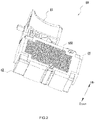
FIG. 2 is a structure view of an integrated electronic switch as a first embodiment; -
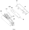
FIG. 3 is an exploded view of an integrated electronic switch inFIG. 2 ; -
FIG. 4 is a structure view of an integrated electronic switch from another angle of view inFIG. 2 ; -
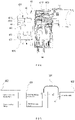
FIG. 5 is a schematic circuit diagram of an integrated electronic switch inFIG. 2 ; -
FIG. 6 is a structure view of an integrated electronic switch inFIG. 2 in which a heat dissipation element and an upper housing are integrally formed; -
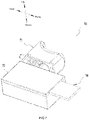
FIG. 7 is a structure view of an integrated electronic switch as a second embodiment; -
FIG. 8 is an exploded view of an integrated electronic switch inFIG. 7 ; -
FIG. 9 is a structure view of an integrated electronic switch as a third embodiment; -
FIG. 10 is an exploded view of an integrated electronic switch inFIG. 9 ; -
FIG. 11 is an exploded view of an integrated electronic switch from another angle of view inFIG. 9 ; -
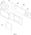
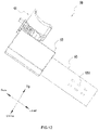
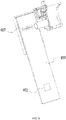
FIG. 12 is a structure view of an integrated electronic switch as a fourth embodiment; -
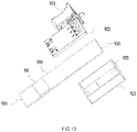
FIG. 13 is an exploded view of an integrated electronic switch inFIG. 12 ; -
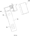
FIG. 14 is an exploded view of an integrated electronic switch from another angle of view inFIG. 12 ; -
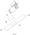
FIG. 15 is a structure view of an integrated electronic switch inFIG. 12 according to another embodiment; and -
FIG. 16 is an exploded view of an integrated electronic switch inFIG. 15 . - The present disclosure is described hereinafter in detail in conjunction with drawings and embodiments. This description is provided with reference to a drill shown in
FIG. 1 , but it is easily understood by those skilled in the art that the technical solution disclosed by the present disclosure can be widely applied to other types of power tools including, but not limited to, a sander, a drill bit, an impact screwdriver, a tapping machine, a fastener screwdriver and the like. The specific embodiments described below are intended to explain but not to limit the present disclosure. Additionally, it is to be noted that for ease of description, only part, not all, of the structures related to the present disclosure are illustrated in the drawings. - Referring to
FIG. 1 , thedrill 100 includes a tool housing, amotor 20, afan 30, agearbox 40 and anoutput portion 50. The tool housing is formed with onehandle 11 for a user to hold. One end of thehandle 11 is connected to a power interface for accessing a direct current (DC) power supply or an alternating current (AC) power supply. In some embodiments, the power interface is connected to abattery pack 200 which is detachably connected to thedrill 100. Apparently, it is understandable that the power port can also be accessed to the alternating current, such as the commercial power. An accommodation space (not shown in the figure) is formed in the tool housing along a firststraight line 101, and themotor 20, thefan 30, and thegearbox 40 are sequentially disposed in the accommodation space. Thedrill 100 also includes an integratedelectronic switch 60 for at least starting the operation of themotor 20 and adjusting a rotational speed of themotor 20. -
FIG. 2 to 5 illustrate an integratedelectronic switch 60 as a first embodiment in the present disclosure. The integratedelectronic switch 60 includes aninput unit 61, ahousing 62, and acircuit board 63 located within thehousing 62. Thehousing 62 includes a sealedaccommodation space 623 formed by anupper housing 621 and a lower housing 622.Thecircuit board 63 is disposed in the accommodation space 623.Theinput unit 61 includes atrigger 611 and asensing actuator 612. Thesensing actuator 612 is provided with a power-on slidingblade 6121 and a speed-regulating slidingblade 6122. The user inputs a drive signal through thetrigger 611. The drive signal includes a power signal and a speed-regulating signal, and thesensing actuator 612 and thetrigger 611 are mechanically connected for transmitting the drive signal inputted by the user. - The
circuit board 63 is provided with asensing module 631, acontrol module 632, and multiple switchingelements 633. Thecontrol module 632 is electrically connected to thesensing module 631 and the multiple switchingelements 633. Thesensing module 631 is configured to sense the drive signal output by theinput unit 61. Thesensing module 631 includes an power-on sensing area 6311 and a speed-regulating sensing area 6312.When the user presses thetrigger 611, thesensing actuator 612 drives the power-on slidingblade 6121 to slide in the power-on sensing area 6311 under the action of thetrigger 611, and the speed-regulating slidingblade 6122 to slide in the speed-regulatingsensing area 6312, and outputs an analog signal corresponding to the drive signal to the control module 632.The speed-regulatingsensing area 6312 is provided with a signal output port a2 for outputting an analog signal corresponding to a speed-regulating signal input by the user, and thecontrol module 632 is provided with one signal input port a1 for receiving the analog signal output from a signal output port a2.ln some embodiments, as shown inFIG. 5 , the signal input port a1 and the signal output port a2 are electrically connected through ajumper 634. Apparently, a resistance may be connected in series between the signal input port a1 and the signal output port a2 for electrical connection through wiring on the circuit board. - Referring to
FIGS. 3 and4 , thecircuit board 63 has afirst side surface 6351 and asecond side surface 6352. In some embodiments, thesensing module 631, thecontrol module 632 and multiple switchingelements 633 are disposed on a same side surface of the circuit board 635. Specifically, thesensing module 631, thecontrol module 632 and multiple switchingelements 633 are disposed on thefirst side surface 6351 of thecircuit board 63. In other embodiments, thesensing module 631 and thecontrol module 632 are disposed on a same side surface of thecircuit board 63. Specifically, thesensing module 631 and thecontrol module 632 are disposed on thefirst side surface 6351 of thecircuit board 63. Themultiple switching elements 633 are disposed on thesecond side surface 6352 of thecircuit board 63. - In this embodiment, the integrated
electronic switch 60 further includes aheat dissipation element 64 for heat dissipation of thecircuit board 63. Theheat dissipation element 64 is at least partially disposed outside the accommodation space 623.In some embodiments, theupper housing 621 is formed with a mounting groove (not shown in the figure) disposed opposite to the multiple switchingelements 633 in an up-down direction. Theheat dissipation element 64 is embedded in the mounting groove. Preferably, theheat dissipation element 64 is configured to be a metal material having a good thermal conductivity. In other embodiments, referring toFIG. 6 , theheat dissipation element 64 is integrally formed with the upper housing 621.lt can be understood that when theheat dissipation element 64 is integrally formed with theupper housing 621 in this embodiment, theupper housing 621 is preferably made of the metal material having a good thermal conductivity. Apparently, other materials having a good thermal conductivity or a heat absorption property may also be used by those skilled in the art to fabricate the housing, which is not limited in the present disclosure. - Referring to
FIG. 2 , the integratedelectronic switch 60 further includes ametal housing 65 disposed on thehousing 62. Specifically, themetal housing 65 is fixed to an outer surface of anupper housing 621 and directly or indirectly contacts with theheat dissipation element 64 on theupper housing 621 to derive heat from the heat dissipation element 64.In this embodiment, themetal housing 65 is secured and mounted to thehousing 62 by screws. To increase the heat dissipation area and enhance the heat dissipation effect, themetal housing 65 is further formed with a hollow grid-shapedheat dissipation area 651 so as to quickly transmit heat generated in theaccommodation space 623 of the integratedelectronic switch 60 to the outside of theaccommodation space 623. - When the
drill 100 works, more heat is generated on multiple switchingelements 633 in the integratedelectronic switch 60. The above heat is firstly transmitted to theheat dissipation element 64 and then to themetal housing 65 to be dissipated into the air. - Referring to
FIG. 4 , the integratedelectronic switch 60 further includes areverse diode 66 for providing a return path for a counter-electromotive force generated by themotor 20 when the integratedelectronic switch 60 is started/stopped, preventing the counter-electromotive force generated by themotor 20 from returning to thebattery pack 200. Thereverse diode 66 is provided outside thehousing 62 of the integratedelectronic switch 60, a negative electrode of thereverse diode 66 is electrically connected to a positive electrode of a power input terminal, and a positive electrode of thereverse diode 66 is electrically connected to a negative electrode of the power input terminal. Apparently, thereverse diode 66 may also be disposed on thecircuit board 63 of the integratedelectronic switch 60. -
FIGS. 7 to 8 illustrate an integratedelectronic switch 70 as a second embodiment in the present disclosure. The integratedelectronic switch 70 includes aninput unit 71, ahousing 72, and acircuit board 73 located within thehousing 72. Thehousing 72 includes a sealedaccommodation space 723 formed by anupper housing 721 and alower housing 722. Thecircuit board 73 is disposed in the accommodation space 723.Theinput unit 71 includes atrigger 711 and a sensing actuator (not shown in the figure). The difference from the first embodiment described above lies in that theheat dissipation element 74 includes a first heat dissipation portion (not shown in the figure) located within theaccommodation space 723 and a secondheat dissipation portion 741 located outside theaccommodation space 723. The first heat dissipation portion is arranged opposite to the multiple switching elements (not shown in the figure) in an up-down direction, and is used for heat dissipation of the multiple switching elements. The first heat dissipation portion of theheat dissipation element 74 is fixed to theupper housing 721, and the secondheat dissipation portion 741 extends outward in a front-rear direction. - In this embodiment, the
heat dissipation element 74 includes the first heat dissipation portion and the secondheat dissipation portion 741 extending in the front-rear direction. The first heat dissipation portion is located in theaccommodation space 723 and is disposed opposite to the multiple switching elements in the up-down direction. The secondheat dissipation portion 741 is located outside theaccommodation space 723, and is configured to rapidly dissipate the heat transmitted from the first heat dissipation portion to the air outside theaccommodation space 723. The assembly difficulty of the integratedelectronic switch 70 in this embodiment is low, and at the same time, the structure of the integratedelectronic switch 70 is simplified. -
FIGS. 9 to 11 illustrates an integratedelectronic switch 80 as a third embodiment in the present disclosure. The integratedelectronic switch 80 includes aninput unit 81, ahousing 82, and acircuit board 83 located within thehousing 82. Theinput unit 81 includes atrigger 811 and a sensing actuator (not shown in the figure). Thehousing 82 includes ahousing bottom 821 and a housing side 822.Thehousing bottom 821 and thehousing side 822 form an open cavity 823.Thecircuit board 83 is disposed in the open cavity 823.Thecircuit board 83 is provided with multiple switchingelements 831 and acontrol module 832. Thehousing bottom 821 has oneheat dissipation hole 824 disposed opposite to the multiple switchingelements 831 in the up-down direction. The integratedelectronic switch 80 further includes onecooling fin 84 disposed opposite to the multiple switching elements in a height direction. Preferably, multiple switchingelements 831 are disposed on afirst side surface 833 of the circuit board 83.Thecontrol module 832 is disposed on thefirst side surface 833 of the circuit board 83.The coolingfin 84 is partially located in the heat dissipation hole 824.Asecond side surface 834 of thecircuit board 83 is sealed through a glue filling process. -
FIGS. 12 to 14 illustrates an integratedelectronic switch 90 as a fourth embodiment in the present disclosure. The integratedelectronic switch 90 includes aninput unit 91, ahousing 92, and acircuit board 93 located within thehousing 92. Theinput unit 91 includes atrigger 911 and a sensing actuator (not shown in the figure). Thehousing 92 includes anupper housing 921 and alower housing 922, and theupper housing 921 and thelower housing 922 are formed with anaccommodation space 923. Thecircuit board 93 includes afirst portion 933 located inside theaccommodation space 923 and asecond portion 934 located outside theaccommodation space 923 extending in a front-rear direction. Thecircuit board 93 is further provided with multiple switchingelements 931, acontrol module 932, and asensing module 937. Further, thecontrol module 932 and thesensing module 937 are disposed in thefirst portion 933 of thecircuit board 93, and multiple switchingelements 931 are disposed in thesecond portion 934 of thecircuit board 93. - In this embodiment, as one possible implementation mode, multiple switching
elements 931, thecontrol module 932, and thesensing module 937 are disposed on a same side surface of thecircuit board 93. Preferably, multiple switchingelements 931 are disposed on thefirst side surface 935 in thesecond portion 934 of thecircuit board 93. Thecontrol module 932 and thesensing module 937 are disposed on thefirst side surface 935 in thefirst portion 933 of the circuit board 93.The integratedelectronic switch 90 in this embodiment further includes aheat dissipation element 94 disposed opposite to the multiple switchingelements 931 in an up-down direction. Theheat dissipation element 94 and the multiple switchingelements 931 are located on both sides of the circuit board 93.ln this embodiment, theheat dissipation element 94 is disposed on thesecond side surface 936 of the circuit board 93.Apparently, theheat dissipation element 94 may also be disposed on a surface of the multiple switchingelements 931. Specifically, a heat conductive member (not shown in the figure) is disposed between theheat dissipation element 94 and the multiple switchingelements 931, and heat from the multiple switchingelements 931 is transmitted to theheat dissipation element 94 by the heat conductive member so as to dissipate the heat from the integratedelectronic switch 90. - As another possible implementation mode, as shown in
FIGS. 15 and16 , thesensing module 937 is disposed in thefirst portion 933 of thecircuit board 93, and thecontrol module 932 and the multiple switchingelements 931 are disposed in thesecond portion 934 of the circuit board 93.Thesensing module 937 and thecontrol module 932 are located on the same side surface of thecircuit board 93, and theheat dissipation element 94 and the multiple switchingelements 931 are located on another side surface of the circuit board 93.Specifically, thesensing module 937 and thecontrol module 932 are disposed on thefirst side surface 935 of thecircuit board 93, and multiple switchingelements 931 and theheat dissipation element 94 are disposed on thesecond side surface 936 of the circuit board 93.In this embodiment, theheat dissipation element 94 is secured and mounted to thecircuit board 93 by screws. - In this embodiment, the circuit board is configured to be two portions. The first portion of the circuit board is disposed in the accommodation space, and the second portion of the circuit board is disposed outside the accommodation space. Multiple switching elements which are easy to generate the heat in the working process of the integrated electronic switch are disposed in the second portion of the circuit board, and at the same time, the heat dissipation element is disposed opposite to the multiple switching elements in the up-down direction for deriving the heat generated by the multiple switching elements. The present disclosure gives more selection space for the position of the heat dissipation element on the integrated electronic switch, and simultaneously reduces the assembly difficulty of the integrated electronic switch.
- The above illustrates and describes basic principles, main features, and advantages of the present disclosure. It is to be understood by those skilled in the art that the preceding embodiments do not limit the present disclosure in any form, and technical solutions obtained by means of equivalent substitution or equivalent transformation fall within the scope of the present disclosure.
Claims (15)
- An integrated electronic switch (60, 70, 80,90), comprising:an input unit (61, 71, 81, 91) configured to receive a drive signal output by a user;a sensing module (631, 937) for sensing the drive signal transmitted from the input unit;a circuit board (63, 73, 83, 93) for supporting the sensing module; anda control module (632, 832, 932) electrically connected to the sensing module anddisposed on the circuit board,wherein the sensing module and the control module are disposed on a first side surface (6351, 833, 935) of the circuit board.
- The integrated electronic switch of claim 1, wherein the circuit board is provided with a plurality of switching elements (633, 831, 931) and the plurality of switching elements are electrically connected to the control module.
- The integrated electronic switch of claim 2, wherein the plurality of switching elements are disposed on a second side surface (6352, 834, 936) of the circuit board and the second side surface is opposite to the first side surface.
- The integrated electronic switch of claim 3, wherein the integrated electronic switch further comprises a heat dissipation element (64, 74, 94) disposed on the second side surface of the circuit board.
- The integrated electronic switch of claim 4, wherein a heat conduction element configured to transmit heat generated on the plurality of switching elements to the heat dissipation element is disposed between the heat dissipation element and the plurality of switching elements.
- The integrated electronic switch of claim 1, wherein the input unit comprises a trigger (611, 711, 811, 911) and a sensing actuator (612), and the sensing actuator is provided with a power-on sliding blade (6121) and a speed-regulating sliding blade (6122).
- The integrated electronic switch of claim 6, wherein the sensing module is formed with a power-on sensing area (6311) and a speed-regulating sensing area (6312), and the power-on sensing area is electrically connected to the power-on sliding blade and the speed-regulating sensing area is electrically connected to the speed-regulating sliding blade when the integrated electronic switch works.
- The integrated electronic switch of claim 1, further comprising a housing (62, 72, 82, 92) formed with an accommodation space (623, 723, 923), wherein the circuit board is at least partially located in the accommodation space.
- The integrated electronic switch of claim 8, wherein the sensing module is disposed in the accommodation space and the control module is disposed outside the accommodation space.
- The integrated electronic switch of claim 1, further comprising a housing (62, 72, 82, 92) formed with an accommodation space (623, 723, 923), wherein the circuit board comprises a first portion (933) located inside the accommodation space and a second portion (934) located outside the accommodation space.
- The integrated electronic switch of claim 10, wherein the sensing module is disposed on the first portion of the circuit board, and the control module is disposed on the second portion of the circuit board.
- The integrated electronic switch of claim 11, wherein the circuit board is provided with a plurality of switching elements (633, 831, 931), the plurality of switching elements are electrically connected to the control module, and the plurality of switching elements is disposed on the second portion of the circuit board.
- The integrated electronic switch of claim 12, further comprising a heat dissipation element (64, 74, 94) for dissipating heat from the switching element.
- The integrated electronic switch of claim 13, wherein the heat dissipation element is located at least partially outside the accommodation space.
- The integrated electronic switch of claim 1, wherein the circuit board is provided with a plurality of switching elements (633, 831, 931), the plurality of switching elements are electrically connected to the control module, and the plurality of switching elements are disposed on the first side surface of the circuit board .
Applications Claiming Priority (3)
| Application Number | Priority Date | Filing Date | Title |
|---|---|---|---|
| CN202110264558 | 2021-03-11 | ||
| CN202210160216.9A CN115087302A (en) | 2021-03-11 | 2022-02-22 | Integrated electronic switch and electric tool |
| CN202210160232.8A CN115083810A (en) | 2021-03-11 | 2022-02-22 | Integrated electronic switch and electric tool |
Publications (2)
| Publication Number | Publication Date |
|---|---|
| EP4057313A1 true EP4057313A1 (en) | 2022-09-14 |
| EP4057313B1 EP4057313B1 (en) | 2023-12-06 |
Family
ID=80685482
Family Applications (1)
| Application Number | Title | Priority Date | Filing Date |
|---|---|---|---|
| EP22161225.2A Active EP4057313B1 (en) | 2021-03-11 | 2022-03-10 | Integrated electronic switch and power tool |
Country Status (2)
| Country | Link |
|---|---|
| US (1) | US11842860B2 (en) |
| EP (1) | EP4057313B1 (en) |
Citations (4)
| Publication number | Priority date | Publication date | Assignee | Title |
|---|---|---|---|---|
| EP2688080A2 (en) * | 2012-07-16 | 2014-01-22 | Black & Decker Inc. | Electronic switching module for a power tool |
| EP2929986A2 (en) * | 2014-03-28 | 2015-10-14 | Black & Decker Inc. | Biasing member for a power tool forward/reverse actuator |
| EP3588525A1 (en) * | 2018-06-28 | 2020-01-01 | Black & Decker Inc. | Electronic switch module with oppositely-arranged power switches and discrete heat sinks |
| WO2020039628A1 (en) * | 2018-08-24 | 2020-02-27 | オムロン株式会社 | Trigger switch |
Family Cites Families (2)
| Publication number | Priority date | Publication date | Assignee | Title |
|---|---|---|---|---|
| US8587231B2 (en) * | 2010-09-28 | 2013-11-19 | Black & Decker Inc. | Method and system for electronic braking of a motor |
| EP3090838B1 (en) * | 2011-05-19 | 2020-06-17 | Black & Decker Inc. | Power tool with force sensing electronic clutch |
-
2022
- 2022-03-10 EP EP22161225.2A patent/EP4057313B1/en active Active
- 2022-03-11 US US17/692,466 patent/US11842860B2/en active Active
Patent Citations (4)
| Publication number | Priority date | Publication date | Assignee | Title |
|---|---|---|---|---|
| EP2688080A2 (en) * | 2012-07-16 | 2014-01-22 | Black & Decker Inc. | Electronic switching module for a power tool |
| EP2929986A2 (en) * | 2014-03-28 | 2015-10-14 | Black & Decker Inc. | Biasing member for a power tool forward/reverse actuator |
| EP3588525A1 (en) * | 2018-06-28 | 2020-01-01 | Black & Decker Inc. | Electronic switch module with oppositely-arranged power switches and discrete heat sinks |
| WO2020039628A1 (en) * | 2018-08-24 | 2020-02-27 | オムロン株式会社 | Trigger switch |
Also Published As
| Publication number | Publication date |
|---|---|
| EP4057313B1 (en) | 2023-12-06 |
| US11842860B2 (en) | 2023-12-12 |
| US20220293358A1 (en) | 2022-09-15 |
Similar Documents
| Publication | Publication Date | Title |
|---|---|---|
| US4719395A (en) | Variable speed control switch for an electric tool including a DC motor | |
| CN204913830U (en) | Electric tool | |
| JP6730418B2 (en) | Electric work machine | |
| JP5630188B2 (en) | Electric tool | |
| EP4046754B1 (en) | Electric tool and electric control assembly thereof | |
| CN201036866Y (en) | Hand-held electric tool | |
| CN101594969A (en) | Power tools with brushless motors | |
| CN114051686B (en) | Electric work machine | |
| JP2018015867A (en) | Electric work machine | |
| US9293964B2 (en) | Power tool | |
| EP4412416A1 (en) | Printed circuit board assembly with multiple conduction paths | |
| JP2004527120A5 (en) | ||
| EP4057313B1 (en) | Integrated electronic switch and power tool | |
| CN216981886U (en) | Hall speed regulation integrated switch and electric tool with same | |
| CN115083810A (en) | Integrated electronic switch and electric tool | |
| JP2014104569A (en) | Power tool | |
| CN206795748U (en) | Electric tool | |
| CN116435118A (en) | Mini DC speed regulating switch | |
| CN206105765U (en) | Electric tool | |
| CN202633092U (en) | Speed regulating switch of electric tool | |
| CN210578321U (en) | Brushless integrated switch and brushless hand-held electric tool | |
| CN222015273U (en) | A push button switch for electric tools | |
| CN219626500U (en) | Mini DC speed regulating switch | |
| US20250345893A1 (en) | Pole power tool and power tool | |
| US20110273036A1 (en) | Power tool having a direct current motor and power electronics |
Legal Events
| Date | Code | Title | Description |
|---|---|---|---|
| PUAI | Public reference made under article 153(3) epc to a published international application that has entered the european phase |
Free format text: ORIGINAL CODE: 0009012 |
|
| STAA | Information on the status of an ep patent application or granted ep patent |
Free format text: STATUS: THE APPLICATION HAS BEEN PUBLISHED |
|
| AK | Designated contracting states |
Kind code of ref document: A1 Designated state(s): AL AT BE BG CH CY CZ DE DK EE ES FI FR GB GR HR HU IE IS IT LI LT LU LV MC MK MT NL NO PL PT RO RS SE SI SK SM TR |
|
| STAA | Information on the status of an ep patent application or granted ep patent |
Free format text: STATUS: REQUEST FOR EXAMINATION WAS MADE |
|
| 17P | Request for examination filed |
Effective date: 20230306 |
|
| RBV | Designated contracting states (corrected) |
Designated state(s): AL AT BE BG CH CY CZ DE DK EE ES FI FR GB GR HR HU IE IS IT LI LT LU LV MC MK MT NL NO PL PT RO RS SE SI SK SM TR |
|
| STAA | Information on the status of an ep patent application or granted ep patent |
Free format text: STATUS: EXAMINATION IS IN PROGRESS |
|
| 17Q | First examination report despatched |
Effective date: 20230420 |
|
| GRAP | Despatch of communication of intention to grant a patent |
Free format text: ORIGINAL CODE: EPIDOSNIGR1 |
|
| STAA | Information on the status of an ep patent application or granted ep patent |
Free format text: STATUS: GRANT OF PATENT IS INTENDED |
|
| GRAS | Grant fee paid |
Free format text: ORIGINAL CODE: EPIDOSNIGR3 |
|
| INTG | Intention to grant announced |
Effective date: 20231002 |
|
| GRAA | (expected) grant |
Free format text: ORIGINAL CODE: 0009210 |
|
| STAA | Information on the status of an ep patent application or granted ep patent |
Free format text: STATUS: THE PATENT HAS BEEN GRANTED |
|
| AK | Designated contracting states |
Kind code of ref document: B1 Designated state(s): AL AT BE BG CH CY CZ DE DK EE ES FI FR GB GR HR HU IE IS IT LI LT LU LV MC MK MT NL NO PL PT RO RS SE SI SK SM TR |
|
| REG | Reference to a national code |
Ref country code: GB Ref legal event code: FG4D |
|
| REG | Reference to a national code |
Ref country code: CH Ref legal event code: EP |
|
| REG | Reference to a national code |
Ref country code: DE Ref legal event code: R096 Ref document number: 602022001193 Country of ref document: DE |
|
| REG | Reference to a national code |
Ref country code: IE Ref legal event code: FG4D |
|
| REG | Reference to a national code |
Ref country code: LT Ref legal event code: MG9D |
|
| PG25 | Lapsed in a contracting state [announced via postgrant information from national office to epo] |
Ref country code: GR Free format text: LAPSE BECAUSE OF FAILURE TO SUBMIT A TRANSLATION OF THE DESCRIPTION OR TO PAY THE FEE WITHIN THE PRESCRIBED TIME-LIMIT Effective date: 20240307 |
|
| REG | Reference to a national code |
Ref country code: NL Ref legal event code: MP Effective date: 20231206 |
|
| PG25 | Lapsed in a contracting state [announced via postgrant information from national office to epo] |
Ref country code: LT Free format text: LAPSE BECAUSE OF FAILURE TO SUBMIT A TRANSLATION OF THE DESCRIPTION OR TO PAY THE FEE WITHIN THE PRESCRIBED TIME-LIMIT Effective date: 20231206 |
|
| PG25 | Lapsed in a contracting state [announced via postgrant information from national office to epo] |
Ref country code: ES Free format text: LAPSE BECAUSE OF FAILURE TO SUBMIT A TRANSLATION OF THE DESCRIPTION OR TO PAY THE FEE WITHIN THE PRESCRIBED TIME-LIMIT Effective date: 20231206 |
|
| PG25 | Lapsed in a contracting state [announced via postgrant information from national office to epo] |
Ref country code: LT Free format text: LAPSE BECAUSE OF FAILURE TO SUBMIT A TRANSLATION OF THE DESCRIPTION OR TO PAY THE FEE WITHIN THE PRESCRIBED TIME-LIMIT Effective date: 20231206 Ref country code: GR Free format text: LAPSE BECAUSE OF FAILURE TO SUBMIT A TRANSLATION OF THE DESCRIPTION OR TO PAY THE FEE WITHIN THE PRESCRIBED TIME-LIMIT Effective date: 20240307 Ref country code: ES Free format text: LAPSE BECAUSE OF FAILURE TO SUBMIT A TRANSLATION OF THE DESCRIPTION OR TO PAY THE FEE WITHIN THE PRESCRIBED TIME-LIMIT Effective date: 20231206 Ref country code: BG Free format text: LAPSE BECAUSE OF FAILURE TO SUBMIT A TRANSLATION OF THE DESCRIPTION OR TO PAY THE FEE WITHIN THE PRESCRIBED TIME-LIMIT Effective date: 20240306 |
|
| REG | Reference to a national code |
Ref country code: AT Ref legal event code: MK05 Ref document number: 1639224 Country of ref document: AT Kind code of ref document: T Effective date: 20231206 |
|
| PG25 | Lapsed in a contracting state [announced via postgrant information from national office to epo] |
Ref country code: NL Free format text: LAPSE BECAUSE OF FAILURE TO SUBMIT A TRANSLATION OF THE DESCRIPTION OR TO PAY THE FEE WITHIN THE PRESCRIBED TIME-LIMIT Effective date: 20231206 |
|
| PG25 | Lapsed in a contracting state [announced via postgrant information from national office to epo] |
Ref country code: SE Free format text: LAPSE BECAUSE OF FAILURE TO SUBMIT A TRANSLATION OF THE DESCRIPTION OR TO PAY THE FEE WITHIN THE PRESCRIBED TIME-LIMIT Effective date: 20231206 Ref country code: RS Free format text: LAPSE BECAUSE OF FAILURE TO SUBMIT A TRANSLATION OF THE DESCRIPTION OR TO PAY THE FEE WITHIN THE PRESCRIBED TIME-LIMIT Effective date: 20231206 Ref country code: NO Free format text: LAPSE BECAUSE OF FAILURE TO SUBMIT A TRANSLATION OF THE DESCRIPTION OR TO PAY THE FEE WITHIN THE PRESCRIBED TIME-LIMIT Effective date: 20240306 Ref country code: NL Free format text: LAPSE BECAUSE OF FAILURE TO SUBMIT A TRANSLATION OF THE DESCRIPTION OR TO PAY THE FEE WITHIN THE PRESCRIBED TIME-LIMIT Effective date: 20231206 Ref country code: LV Free format text: LAPSE BECAUSE OF FAILURE TO SUBMIT A TRANSLATION OF THE DESCRIPTION OR TO PAY THE FEE WITHIN THE PRESCRIBED TIME-LIMIT Effective date: 20231206 Ref country code: HR Free format text: LAPSE BECAUSE OF FAILURE TO SUBMIT A TRANSLATION OF THE DESCRIPTION OR TO PAY THE FEE WITHIN THE PRESCRIBED TIME-LIMIT Effective date: 20231206 |
|
| PG25 | Lapsed in a contracting state [announced via postgrant information from national office to epo] |
Ref country code: IS Free format text: LAPSE BECAUSE OF FAILURE TO SUBMIT A TRANSLATION OF THE DESCRIPTION OR TO PAY THE FEE WITHIN THE PRESCRIBED TIME-LIMIT Effective date: 20240406 |
|
| PG25 | Lapsed in a contracting state [announced via postgrant information from national office to epo] |
Ref country code: AT Free format text: LAPSE BECAUSE OF FAILURE TO SUBMIT A TRANSLATION OF THE DESCRIPTION OR TO PAY THE FEE WITHIN THE PRESCRIBED TIME-LIMIT Effective date: 20231206 Ref country code: CZ Free format text: LAPSE BECAUSE OF FAILURE TO SUBMIT A TRANSLATION OF THE DESCRIPTION OR TO PAY THE FEE WITHIN THE PRESCRIBED TIME-LIMIT Effective date: 20231206 |
|
| PG25 | Lapsed in a contracting state [announced via postgrant information from national office to epo] |
Ref country code: SK Free format text: LAPSE BECAUSE OF FAILURE TO SUBMIT A TRANSLATION OF THE DESCRIPTION OR TO PAY THE FEE WITHIN THE PRESCRIBED TIME-LIMIT Effective date: 20231206 |
|
| PG25 | Lapsed in a contracting state [announced via postgrant information from national office to epo] |
Ref country code: SM Free format text: LAPSE BECAUSE OF FAILURE TO SUBMIT A TRANSLATION OF THE DESCRIPTION OR TO PAY THE FEE WITHIN THE PRESCRIBED TIME-LIMIT Effective date: 20231206 Ref country code: SK Free format text: LAPSE BECAUSE OF FAILURE TO SUBMIT A TRANSLATION OF THE DESCRIPTION OR TO PAY THE FEE WITHIN THE PRESCRIBED TIME-LIMIT Effective date: 20231206 Ref country code: RO Free format text: LAPSE BECAUSE OF FAILURE TO SUBMIT A TRANSLATION OF THE DESCRIPTION OR TO PAY THE FEE WITHIN THE PRESCRIBED TIME-LIMIT Effective date: 20231206 Ref country code: IT Free format text: LAPSE BECAUSE OF FAILURE TO SUBMIT A TRANSLATION OF THE DESCRIPTION OR TO PAY THE FEE WITHIN THE PRESCRIBED TIME-LIMIT Effective date: 20231206 Ref country code: IS Free format text: LAPSE BECAUSE OF FAILURE TO SUBMIT A TRANSLATION OF THE DESCRIPTION OR TO PAY THE FEE WITHIN THE PRESCRIBED TIME-LIMIT Effective date: 20240406 Ref country code: EE Free format text: LAPSE BECAUSE OF FAILURE TO SUBMIT A TRANSLATION OF THE DESCRIPTION OR TO PAY THE FEE WITHIN THE PRESCRIBED TIME-LIMIT Effective date: 20231206 Ref country code: CZ Free format text: LAPSE BECAUSE OF FAILURE TO SUBMIT A TRANSLATION OF THE DESCRIPTION OR TO PAY THE FEE WITHIN THE PRESCRIBED TIME-LIMIT Effective date: 20231206 Ref country code: AT Free format text: LAPSE BECAUSE OF FAILURE TO SUBMIT A TRANSLATION OF THE DESCRIPTION OR TO PAY THE FEE WITHIN THE PRESCRIBED TIME-LIMIT Effective date: 20231206 |
|
| PG25 | Lapsed in a contracting state [announced via postgrant information from national office to epo] |
Ref country code: PL Free format text: LAPSE BECAUSE OF FAILURE TO SUBMIT A TRANSLATION OF THE DESCRIPTION OR TO PAY THE FEE WITHIN THE PRESCRIBED TIME-LIMIT Effective date: 20231206 Ref country code: PT Free format text: LAPSE BECAUSE OF FAILURE TO SUBMIT A TRANSLATION OF THE DESCRIPTION OR TO PAY THE FEE WITHIN THE PRESCRIBED TIME-LIMIT Effective date: 20240408 |
|
| PG25 | Lapsed in a contracting state [announced via postgrant information from national office to epo] |
Ref country code: PT Free format text: LAPSE BECAUSE OF FAILURE TO SUBMIT A TRANSLATION OF THE DESCRIPTION OR TO PAY THE FEE WITHIN THE PRESCRIBED TIME-LIMIT Effective date: 20240408 Ref country code: PL Free format text: LAPSE BECAUSE OF FAILURE TO SUBMIT A TRANSLATION OF THE DESCRIPTION OR TO PAY THE FEE WITHIN THE PRESCRIBED TIME-LIMIT Effective date: 20231206 |
|
| REG | Reference to a national code |
Ref country code: DE Ref legal event code: R097 Ref document number: 602022001193 Country of ref document: DE |
|
| PG25 | Lapsed in a contracting state [announced via postgrant information from national office to epo] |
Ref country code: DK Free format text: LAPSE BECAUSE OF FAILURE TO SUBMIT A TRANSLATION OF THE DESCRIPTION OR TO PAY THE FEE WITHIN THE PRESCRIBED TIME-LIMIT Effective date: 20231206 |
|
| PLBE | No opposition filed within time limit |
Free format text: ORIGINAL CODE: 0009261 |
|
| STAA | Information on the status of an ep patent application or granted ep patent |
Free format text: STATUS: NO OPPOSITION FILED WITHIN TIME LIMIT |
|
| PG25 | Lapsed in a contracting state [announced via postgrant information from national office to epo] |
Ref country code: SI Free format text: LAPSE BECAUSE OF FAILURE TO SUBMIT A TRANSLATION OF THE DESCRIPTION OR TO PAY THE FEE WITHIN THE PRESCRIBED TIME-LIMIT Effective date: 20231206 |
|
| PG25 | Lapsed in a contracting state [announced via postgrant information from national office to epo] |
Ref country code: SI Free format text: LAPSE BECAUSE OF FAILURE TO SUBMIT A TRANSLATION OF THE DESCRIPTION OR TO PAY THE FEE WITHIN THE PRESCRIBED TIME-LIMIT Effective date: 20231206 Ref country code: DK Free format text: LAPSE BECAUSE OF FAILURE TO SUBMIT A TRANSLATION OF THE DESCRIPTION OR TO PAY THE FEE WITHIN THE PRESCRIBED TIME-LIMIT Effective date: 20231206 |
|
| 26N | No opposition filed |
Effective date: 20240909 |
|
| PG25 | Lapsed in a contracting state [announced via postgrant information from national office to epo] |
Ref country code: LU Free format text: LAPSE BECAUSE OF NON-PAYMENT OF DUE FEES Effective date: 20240310 |
|
| PG25 | Lapsed in a contracting state [announced via postgrant information from national office to epo] |
Ref country code: MC Free format text: LAPSE BECAUSE OF FAILURE TO SUBMIT A TRANSLATION OF THE DESCRIPTION OR TO PAY THE FEE WITHIN THE PRESCRIBED TIME-LIMIT Effective date: 20231206 |
|
| PG25 | Lapsed in a contracting state [announced via postgrant information from national office to epo] |
Ref country code: MC Free format text: LAPSE BECAUSE OF FAILURE TO SUBMIT A TRANSLATION OF THE DESCRIPTION OR TO PAY THE FEE WITHIN THE PRESCRIBED TIME-LIMIT Effective date: 20231206 Ref country code: LU Free format text: LAPSE BECAUSE OF NON-PAYMENT OF DUE FEES Effective date: 20240310 |
|
| REG | Reference to a national code |
Ref country code: BE Ref legal event code: MM Effective date: 20240331 |
|
| PG25 | Lapsed in a contracting state [announced via postgrant information from national office to epo] |
Ref country code: BE Free format text: LAPSE BECAUSE OF NON-PAYMENT OF DUE FEES Effective date: 20240331 |
|
| PG25 | Lapsed in a contracting state [announced via postgrant information from national office to epo] |
Ref country code: IE Free format text: LAPSE BECAUSE OF NON-PAYMENT OF DUE FEES Effective date: 20240310 |
|
| PG25 | Lapsed in a contracting state [announced via postgrant information from national office to epo] |
Ref country code: IE Free format text: LAPSE BECAUSE OF NON-PAYMENT OF DUE FEES Effective date: 20240310 Ref country code: BE Free format text: LAPSE BECAUSE OF NON-PAYMENT OF DUE FEES Effective date: 20240331 |
|
| PG25 | Lapsed in a contracting state [announced via postgrant information from national office to epo] |
Ref country code: CY Free format text: LAPSE BECAUSE OF FAILURE TO SUBMIT A TRANSLATION OF THE DESCRIPTION OR TO PAY THE FEE WITHIN THE PRESCRIBED TIME-LIMIT; INVALID AB INITIO Effective date: 20220310 |
|
| PG25 | Lapsed in a contracting state [announced via postgrant information from national office to epo] |
Ref country code: FI Free format text: LAPSE BECAUSE OF FAILURE TO SUBMIT A TRANSLATION OF THE DESCRIPTION OR TO PAY THE FEE WITHIN THE PRESCRIBED TIME-LIMIT Effective date: 20231207 |
|
| REG | Reference to a national code |
Ref country code: CH Ref legal event code: H13 Free format text: ST27 STATUS EVENT CODE: U-0-0-H10-H13 (AS PROVIDED BY THE NATIONAL OFFICE) Effective date: 20251023 |
|
| PG25 | Lapsed in a contracting state [announced via postgrant information from national office to epo] |
Ref country code: TR Free format text: LAPSE BECAUSE OF FAILURE TO SUBMIT A TRANSLATION OF THE DESCRIPTION OR TO PAY THE FEE WITHIN THE PRESCRIBED TIME-LIMIT Effective date: 20231206 |
|
| PG25 | Lapsed in a contracting state [announced via postgrant information from national office to epo] |
Ref country code: CH Free format text: LAPSE BECAUSE OF NON-PAYMENT OF DUE FEES Effective date: 20250331 |
|
| PGFP | Annual fee paid to national office [announced via postgrant information from national office to epo] |
Ref country code: GB Payment date: 20260202 Year of fee payment: 5 |
|
| PGFP | Annual fee paid to national office [announced via postgrant information from national office to epo] |
Ref country code: DE Payment date: 20260128 Year of fee payment: 5 |
|
| PGFP | Annual fee paid to national office [announced via postgrant information from national office to epo] |
Ref country code: FR Payment date: 20260209 Year of fee payment: 5 |