EP4057067A1 - Microstructure and method for manufacturing same - Google Patents
Microstructure and method for manufacturing same Download PDFInfo
- Publication number
- EP4057067A1 EP4057067A1 EP20885957.9A EP20885957A EP4057067A1 EP 4057067 A1 EP4057067 A1 EP 4057067A1 EP 20885957 A EP20885957 A EP 20885957A EP 4057067 A1 EP4057067 A1 EP 4057067A1
- Authority
- EP
- European Patent Office
- Prior art keywords
- microstructure
- energy ray
- resin
- pores
- resin layer
- Prior art date
- Legal status (The legal status is an assumption and is not a legal conclusion. Google has not performed a legal analysis and makes no representation as to the accuracy of the status listed.)
- Withdrawn
Links
Images





Classifications
-
- G—PHYSICS
- G02—OPTICS
- G02B—OPTICAL ELEMENTS, SYSTEMS OR APPARATUS
- G02B1/00—Optical elements characterised by the material of which they are made; Optical coatings for optical elements
- G02B1/02—Optical elements characterised by the material of which they are made; Optical coatings for optical elements made of crystals, e.g. rock-salt, semi-conductors
-
- G—PHYSICS
- G02—OPTICS
- G02B—OPTICAL ELEMENTS, SYSTEMS OR APPARATUS
- G02B1/00—Optical elements characterised by the material of which they are made; Optical coatings for optical elements
- G02B1/04—Optical elements characterised by the material of which they are made; Optical coatings for optical elements made of organic materials, e.g. plastics
-
- B—PERFORMING OPERATIONS; TRANSPORTING
- B33—ADDITIVE MANUFACTURING TECHNOLOGY
- B33Y—ADDITIVE MANUFACTURING, i.e. MANUFACTURING OF THREE-DIMENSIONAL [3D] OBJECTS BY ADDITIVE DEPOSITION, ADDITIVE AGGLOMERATION OR ADDITIVE LAYERING, e.g. BY 3D PRINTING, STEREOLITHOGRAPHY OR SELECTIVE LASER SINTERING
- B33Y80/00—Products made by additive manufacturing
-
- B—PERFORMING OPERATIONS; TRANSPORTING
- B29—WORKING OF PLASTICS; WORKING OF SUBSTANCES IN A PLASTIC STATE IN GENERAL
- B29D—PRODUCING PARTICULAR ARTICLES FROM PLASTICS OR FROM SUBSTANCES IN A PLASTIC STATE
- B29D11/00—Producing optical elements, e.g. lenses or prisms
- B29D11/0074—Production of other optical elements not provided for in B29D11/00009- B29D11/0073
- B29D11/00769—Producing diffraction gratings
-
- B—PERFORMING OPERATIONS; TRANSPORTING
- B29—WORKING OF PLASTICS; WORKING OF SUBSTANCES IN A PLASTIC STATE IN GENERAL
- B29D—PRODUCING PARTICULAR ARTICLES FROM PLASTICS OR FROM SUBSTANCES IN A PLASTIC STATE
- B29D11/00—Producing optical elements, e.g. lenses or prisms
- B29D11/00865—Applying coatings; tinting; colouring
- B29D11/00884—Spin coating
-
- G—PHYSICS
- G02—OPTICS
- G02B—OPTICAL ELEMENTS, SYSTEMS OR APPARATUS
- G02B1/00—Optical elements characterised by the material of which they are made; Optical coatings for optical elements
- G02B1/002—Optical elements characterised by the material of which they are made; Optical coatings for optical elements made of materials engineered to provide properties not available in nature, e.g. metamaterials
- G02B1/005—Optical elements characterised by the material of which they are made; Optical coatings for optical elements made of materials engineered to provide properties not available in nature, e.g. metamaterials made of photonic crystals or photonic band gap materials
-
- G—PHYSICS
- G02—OPTICS
- G02B—OPTICAL ELEMENTS, SYSTEMS OR APPARATUS
- G02B5/00—Optical elements other than lenses
-
- G—PHYSICS
- G03—PHOTOGRAPHY; CINEMATOGRAPHY; ANALOGOUS TECHNIQUES USING WAVES OTHER THAN OPTICAL WAVES; ELECTROGRAPHY; HOLOGRAPHY
- G03F—PHOTOMECHANICAL PRODUCTION OF TEXTURED OR PATTERNED SURFACES, e.g. FOR PRINTING, FOR PROCESSING OF SEMICONDUCTOR DEVICES; MATERIALS THEREFOR; ORIGINALS THEREFOR; APPARATUS SPECIALLY ADAPTED THEREFOR
- G03F7/00—Photomechanical, e.g. photolithographic, production of textured or patterned surfaces, e.g. printing surfaces; Materials therefor, e.g. comprising photoresists; Apparatus specially adapted therefor
- G03F7/0037—Production of three-dimensional images
-
- G—PHYSICS
- G03—PHOTOGRAPHY; CINEMATOGRAPHY; ANALOGOUS TECHNIQUES USING WAVES OTHER THAN OPTICAL WAVES; ELECTROGRAPHY; HOLOGRAPHY
- G03F—PHOTOMECHANICAL PRODUCTION OF TEXTURED OR PATTERNED SURFACES, e.g. FOR PRINTING, FOR PROCESSING OF SEMICONDUCTOR DEVICES; MATERIALS THEREFOR; ORIGINALS THEREFOR; APPARATUS SPECIALLY ADAPTED THEREFOR
- G03F7/00—Photomechanical, e.g. photolithographic, production of textured or patterned surfaces, e.g. printing surfaces; Materials therefor, e.g. comprising photoresists; Apparatus specially adapted therefor
- G03F7/004—Photosensitive materials
- G03F7/039—Macromolecular compounds which are photodegradable, e.g. positive electron resists
-
- G—PHYSICS
- G03—PHOTOGRAPHY; CINEMATOGRAPHY; ANALOGOUS TECHNIQUES USING WAVES OTHER THAN OPTICAL WAVES; ELECTROGRAPHY; HOLOGRAPHY
- G03F—PHOTOMECHANICAL PRODUCTION OF TEXTURED OR PATTERNED SURFACES, e.g. FOR PRINTING, FOR PROCESSING OF SEMICONDUCTOR DEVICES; MATERIALS THEREFOR; ORIGINALS THEREFOR; APPARATUS SPECIALLY ADAPTED THEREFOR
- G03F7/00—Photomechanical, e.g. photolithographic, production of textured or patterned surfaces, e.g. printing surfaces; Materials therefor, e.g. comprising photoresists; Apparatus specially adapted therefor
- G03F7/20—Exposure; Apparatus therefor
- G03F7/2002—Exposure; Apparatus therefor with visible light or UV light, through an original having an opaque pattern on a transparent support, e.g. film printing, projection printing; by reflection of visible or UV light from an original such as a printed image
- G03F7/201—Exposure; Apparatus therefor with visible light or UV light, through an original having an opaque pattern on a transparent support, e.g. film printing, projection printing; by reflection of visible or UV light from an original such as a printed image characterised by an oblique exposure; characterised by the use of plural sources; characterised by the rotation of the optical device; characterised by a relative movement of the optical device, the light source, the sensitive system or the mask
-
- G—PHYSICS
- G03—PHOTOGRAPHY; CINEMATOGRAPHY; ANALOGOUS TECHNIQUES USING WAVES OTHER THAN OPTICAL WAVES; ELECTROGRAPHY; HOLOGRAPHY
- G03F—PHOTOMECHANICAL PRODUCTION OF TEXTURED OR PATTERNED SURFACES, e.g. FOR PRINTING, FOR PROCESSING OF SEMICONDUCTOR DEVICES; MATERIALS THEREFOR; ORIGINALS THEREFOR; APPARATUS SPECIALLY ADAPTED THEREFOR
- G03F7/00—Photomechanical, e.g. photolithographic, production of textured or patterned surfaces, e.g. printing surfaces; Materials therefor, e.g. comprising photoresists; Apparatus specially adapted therefor
- G03F7/20—Exposure; Apparatus therefor
- G03F7/2002—Exposure; Apparatus therefor with visible light or UV light, through an original having an opaque pattern on a transparent support, e.g. film printing, projection printing; by reflection of visible or UV light from an original such as a printed image
- G03F7/2014—Contact or film exposure of light sensitive plates such as lithographic plates or circuit boards, e.g. in a vacuum frame
-
- G—PHYSICS
- G03—PHOTOGRAPHY; CINEMATOGRAPHY; ANALOGOUS TECHNIQUES USING WAVES OTHER THAN OPTICAL WAVES; ELECTROGRAPHY; HOLOGRAPHY
- G03F—PHOTOMECHANICAL PRODUCTION OF TEXTURED OR PATTERNED SURFACES, e.g. FOR PRINTING, FOR PROCESSING OF SEMICONDUCTOR DEVICES; MATERIALS THEREFOR; ORIGINALS THEREFOR; APPARATUS SPECIALLY ADAPTED THEREFOR
- G03F7/00—Photomechanical, e.g. photolithographic, production of textured or patterned surfaces, e.g. printing surfaces; Materials therefor, e.g. comprising photoresists; Apparatus specially adapted therefor
- G03F7/20—Exposure; Apparatus therefor
- G03F7/2022—Multi-step exposure, e.g. hybrid; backside exposure; blanket exposure, e.g. for image reversal; edge exposure, e.g. for edge bead removal; corrective exposure
- G03F7/203—Multi-step exposure, e.g. hybrid; backside exposure; blanket exposure, e.g. for image reversal; edge exposure, e.g. for edge bead removal; corrective exposure comprising an imagewise exposure to electromagnetic radiation or corpuscular radiation
-
- G—PHYSICS
- G03—PHOTOGRAPHY; CINEMATOGRAPHY; ANALOGOUS TECHNIQUES USING WAVES OTHER THAN OPTICAL WAVES; ELECTROGRAPHY; HOLOGRAPHY
- G03F—PHOTOMECHANICAL PRODUCTION OF TEXTURED OR PATTERNED SURFACES, e.g. FOR PRINTING, FOR PROCESSING OF SEMICONDUCTOR DEVICES; MATERIALS THEREFOR; ORIGINALS THEREFOR; APPARATUS SPECIALLY ADAPTED THEREFOR
- G03F7/00—Photomechanical, e.g. photolithographic, production of textured or patterned surfaces, e.g. printing surfaces; Materials therefor, e.g. comprising photoresists; Apparatus specially adapted therefor
- G03F7/70—Microphotolithographic exposure; Apparatus therefor
- G03F7/70216—Mask projection systems
- G03F7/70316—Details of optical elements, e.g. of Bragg reflectors, extreme ultraviolet [EUV] multilayer or bilayer mirrors or diffractive optical elements
-
- G—PHYSICS
- G03—PHOTOGRAPHY; CINEMATOGRAPHY; ANALOGOUS TECHNIQUES USING WAVES OTHER THAN OPTICAL WAVES; ELECTROGRAPHY; HOLOGRAPHY
- G03F—PHOTOMECHANICAL PRODUCTION OF TEXTURED OR PATTERNED SURFACES, e.g. FOR PRINTING, FOR PROCESSING OF SEMICONDUCTOR DEVICES; MATERIALS THEREFOR; ORIGINALS THEREFOR; APPARATUS SPECIALLY ADAPTED THEREFOR
- G03F7/00—Photomechanical, e.g. photolithographic, production of textured or patterned surfaces, e.g. printing surfaces; Materials therefor, e.g. comprising photoresists; Apparatus specially adapted therefor
- G03F7/70—Microphotolithographic exposure; Apparatus therefor
- G03F7/70408—Interferometric lithography; Holographic lithography; Self-imaging lithography, e.g. utilizing the Talbot effect
-
- G—PHYSICS
- G03—PHOTOGRAPHY; CINEMATOGRAPHY; ANALOGOUS TECHNIQUES USING WAVES OTHER THAN OPTICAL WAVES; ELECTROGRAPHY; HOLOGRAPHY
- G03F—PHOTOMECHANICAL PRODUCTION OF TEXTURED OR PATTERNED SURFACES, e.g. FOR PRINTING, FOR PROCESSING OF SEMICONDUCTOR DEVICES; MATERIALS THEREFOR; ORIGINALS THEREFOR; APPARATUS SPECIALLY ADAPTED THEREFOR
- G03F7/00—Photomechanical, e.g. photolithographic, production of textured or patterned surfaces, e.g. printing surfaces; Materials therefor, e.g. comprising photoresists; Apparatus specially adapted therefor
- G03F7/70—Microphotolithographic exposure; Apparatus therefor
- G03F7/70416—2.5D lithography
-
- G—PHYSICS
- G03—PHOTOGRAPHY; CINEMATOGRAPHY; ANALOGOUS TECHNIQUES USING WAVES OTHER THAN OPTICAL WAVES; ELECTROGRAPHY; HOLOGRAPHY
- G03F—PHOTOMECHANICAL PRODUCTION OF TEXTURED OR PATTERNED SURFACES, e.g. FOR PRINTING, FOR PROCESSING OF SEMICONDUCTOR DEVICES; MATERIALS THEREFOR; ORIGINALS THEREFOR; APPARATUS SPECIALLY ADAPTED THEREFOR
- G03F7/00—Photomechanical, e.g. photolithographic, production of textured or patterned surfaces, e.g. printing surfaces; Materials therefor, e.g. comprising photoresists; Apparatus specially adapted therefor
- G03F7/70—Microphotolithographic exposure; Apparatus therefor
- G03F7/70425—Imaging strategies, e.g. for increasing throughput or resolution, printing product fields larger than the image field or compensating lithography- or non-lithography errors, e.g. proximity correction, mix-and-match, stitching or double patterning
- G03F7/70466—Multiple exposures, e.g. combination of fine and coarse exposures, double patterning or multiple exposures for printing a single feature
-
- G—PHYSICS
- G02—OPTICS
- G02B—OPTICAL ELEMENTS, SYSTEMS OR APPARATUS
- G02B2207/00—Coding scheme for general features or characteristics of optical elements and systems of subclass G02B, but not including elements and systems which would be classified in G02B6/00 and subgroups
- G02B2207/101—Nanooptics
-
- G—PHYSICS
- G02—OPTICS
- G02B—OPTICAL ELEMENTS, SYSTEMS OR APPARATUS
- G02B5/00—Optical elements other than lenses
- G02B5/18—Diffraction gratings
- G02B5/1847—Manufacturing methods
Definitions
- the present invention relates to microstructures processed using the Talbot effect and a method for producing the same.
- Submicron three-dimensional structures have drawn attention recently.
- Examples of the submicron three-dimensional structures include microstructured parts for semiconductor devices and microelectromechanical systems (MEMS), biomimetic structures that imitate functional microstructures of living organisms, and nanostructured photonic crystals composed of substances with different refractive indexes arranged at intervals almost the same as light wavelength.
- MEMS microelectromechanical systems
- These submicron three-dimensional structures, particularly those having a periodic structure are attracting attention as functional materials.
- Techniques for fabricating microstructures include lithography, etching, nanoimprint, laser micromachining, atomic manipulation using an atomic force microscope (AFM), and self-organization. These techniques require longer processing time as structures are formed multidimensionally, and improved processing efficiency is required.
- a high degree of freedom and high accuracy in processing are also required, along with more complicated structures, to control the periodic structure as desired.
- the efficiency and the degree of freedom in processing are in a trade-off relationship, and technologies for fabricating multi-dimensional microstructures with a simple technique have not yet been established and are under development. Together with the improvement in the processing accuracy, it also is desired to broaden a processing area to the order of millimeters in the production of microstructures.
- One simple method for producing microstructures is a three-dimensional lithography technique using a resist resin material.
- three-dimensional lithography using the Talbot effect facilitates the formation of a periodic pattern in a large area at once by using a specific wavelength and a diffraction grating, and highly improves the processing efficiency.
- the degree of freedom in processing is low, because the parameters for controlling the periodicity are the wavelength and the grating pitch, and thus the period control is limited to two dimensions.
- No technologies have been established for processing three-dimensional structures into desired shapes without limiting the processing area to the "surface" or "inside".
- Patent Document 1 discloses lithography techniques using the Talbot effect. These techniques are intended for processing with use of etching screen masks and do not involve internal processing of structures. Patent Document 2 discloses masks and pattern forming methods that enable highly accurate patterns to be formed using the Talbot effect, but the technique is not intended for fabrication of structures. Patent Document 3 discloses formation of periodic recesses or pores by etching, but it is not easy to fabricate microstructures with this technique. Non-Patent Document 1 proposes a structure in which metal nanoparticles are dispersed by applying stereolithography using the Talbot effect, but the technique has not reached fabricating clear layer structures using the Talbot effect.
- Non-Patent Document 2 discloses fabrication of nanostructures in a large area in one-dimensional layer structures and two-dimensional periodic structures, but the accuracy and the maintenance of the structures are unsatisfactory, and the technique has not reached fabricating periodic structures.
- Non-Patent Document 3 and Non-Patent Document 4 suggest the possibility of fabricating three-dimensional periodic nanostructures based on the results of numerical analysis of multiple exposures, but the accuracy and the maintenance of the structures are unsatisfactory, and the technique has not yet reached fabricating commercially practical structures.
- the present invention provides three-dimensional microfabricated structures having controlled periodicity from the surface to the inside.
- the present invention relates to a microstructure having pores on its surface or inside,
- a method for producing the microstructure of the present invention is a method for producing the microstructure according to any of claims 1 to 6, including:
- Multiple exposure including exposure with rotation and/or shifting in the triaxial direction of energy ray obtained by the Talbot effect, enables formation of pores on the surface or inside of structures, whereby the microstructure of the present invention has controlled periodicity from the surface to the inside.
- a sheet containing an energy ray active resin has pores formed in a vertical array.
- the pores may be present on the surface or inside of the sheet.
- the pores may be either closed or open.
- the pores in the microstructure are in a formation pattern with a Talbot distance being specified by Formula 1 above.
- the pores have a periodic shape in the planar direction.
- the energy ray active resin is preferably a resist resin, and more preferably a positive resist resin. Portions in the positive resist resin exposed to energy ray dissolve in a solution, and such a property of the positive resist resin is suitable for microfabrication. A negative resist resin is exposed to high temperatures in postbaking, which strains resin and makes it difficult to produce microstructures with accurate periodicity.
- the periodic shape preferably satisfies a grating pitch of wavelength ⁇ grating pitch d and a pitch duty cycle of 0.2 to 0.7. This makes is possible to perform finer processing.
- the periodic shape is preferably a shape with regularity. Thus, microstructures with high uniformity are obtained.
- the pores on the surface or inside of the microstructure include closed cells, pores penetrating through the front and back surfaces of the microstructure, grooves, holes, and other various pores.
- the production method of the microstructure of the present invention includes the following steps:
- An exemplary technique for the application of an energy ray active resin in a uniform thickness in (1) is spin coating.
- the spin coating enables thin and uniform application in a relatively small area.
- Preferable conditions for the prebaking (heating) in (2) are the temperature of 0°C to 100°C and the time of about 1 to 5 minutes, according to the manufactures' recommendation.
- Preferable conditions for the vertical irradiation with energy ray in the pattern forming step in (3) are the number of times of exposure of 2 to 10 times and the total exposure dose of 100 to 300 mJ/cm 2 .
- the exposure with energy ray obtained by the Talbot effect may be any of the following: multiple exposures from the vertical direction; multiple exposures with shifting in the triaxial direction or rotation: or multiple exposures with shifting in the triaxial direction and rotation.
- either the substrate or the diffraction grating may be moved, and any common positioning device may be used.
- Postbaking is preferably performed between (3) and (4) to stabilize the exposed resist.
- Preferable conditions for the postbaking are the temperature of 30°C to 100°C and the time of about 1 to 60 minutes.
- An exemplary technique for the washing in (5) is spin coating.
- the Talbot effect used in the present invention is as follows.
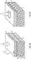
- FIG. 1A is a schematic cross-sectional view illustrating the basic concept of the present invention in which an optical filter (exposure mask) 2 is placed on the upper surface of a photoresist resin 3 and irradiated with ultraviolet light (UV) 1.
- the photoresist resin 3 is a positive photoresist resin
- the optical filter (exposure mask) 2 is, e.g., a polycarbonate diffraction grating.
- a space between the photoresist resin 3 and the optical filter (exposure mask) 2 is defined as a distance 1.
- X and Y indicate the planar direction, and Z indicates the depth direction. Details are shown in the drawing.
- FIG. 1B is a schematic cross-sectional view illustrating light exposed portions 4, irradiated with light, in the photoresist resin 3.
- the pattern of dots indicates the exposed light intensity distribution, where the larger the number of dots, the higher the exposure intensity.
- the exposure intensity is standardized by the strongest light intensity and expressed in an arbitrary unit, a.u.
- FIG. 2A is a schematic perspective view illustrating multiple exposures in one embodiment of the present invention.
- Vertically irradiating the surface of the photoresist resin 3 with ultraviolet light (UV) 1 yields light exposed portions 5a and 5b.
- Z T is a Talbot distance (nm).
- the Talbot distance is a vertical distance (nm) between the center of an irradiated spot in the first row and the center of an irradiated spot in the third row, these irradiated spots being on the same irradiation line as viewed from the irradiation surface.
- FIG. 2B is a schematic perspective view illustrating an exposure involving rotation.
- the rotation is the rotation of the photoresist resin 3 by a predetermined angle ⁇ .
- light exposed portions 7 are independent of each other and become closed pores when dissolved in the following step.
- FIGS. 3A to 3E are schematic cross-sectional views and FIG. 3F is a schematic perspective view illustrating a production method in one embodiment of the present invention.
- Preferable processing conditions according to the present invention are as follows.
- Resin material A positive resist is preferably used.
- a positive UV curable resin is preferred.
- a negative resist requires a step of arranging a buffer layer and involves high temperature exposure in postbaking, which strains the resin and makes it difficult to produce microstructures with accurate periodicity.
- the processing temperature (prebaking) of resin is preferably 0 to 100°C. This is the resin curing temperature range according to the resin manufactures' recommendation.
- Examples of the energy ray include ultraviolet lights (UV-A, B, C), X-rays, and electron beams.
- Diffraction grating One or more optical filters are used. For example, polycarbonate optical filters are used.
- the grating pitch is specified by wavelength ⁇ ⁇ grating pitch d.
- the pitch duty cycle is 0.2 to 0.7, and preferably 0.4 to 0.6.
- the grating pitch is 747 nm, and the grating height is 150 nm.
- the DVD surface can be used as a diffraction grating. Examples of the diffraction grating other than DVDs include those described in Table 1.
- the experiment was performed in the following manner.
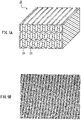
- FIG. 4 shows an obtained microstructure (sheet) 20, in which closed pores 22 are regularly formed with periodicity inside a resin portion 21.
- Microstructures of Examples 2 to 7 were produced in the same manner as in Example 1 except for conditions described in Table 2.
- FIG. 5A is a schematic perspective view illustrating the inside of a microstructure of Example 2, and FIG. 5B is a photograph of the same.
- FIG. 6 is a schematic perspective view illustrating the inside of a microstructure of Example 3.
- FIG. 7 is a schematic perspective view illustrating the inside of a microstructure of Example 4.
- FIG. 8 is a schematic perspective view illustrating the inside of a microstructure of Example 5.
- FIG. 9A is a schematic perspective view illustrating the inside of a microstructure of Example 6, and FIG. 9B is a photograph of the same.
- FIG. 10 is a schematic perspective view illustrating the inside of a microstructure of Example 7. In FIGS.
- FIGS. 5A and 5B FIG. 6 FIG. 7 [Table 3]
- Example 5 Example 6
- microstructures of the present invention having a resin layer in which grooves, through pores, open cells, and the like are formed, are applicable to photonic structures including filters, biomimetic structures, functional members, etc.
Landscapes
- Physics & Mathematics (AREA)
- General Physics & Mathematics (AREA)
- Engineering & Computer Science (AREA)
- Optics & Photonics (AREA)
- Manufacturing & Machinery (AREA)
- Chemical & Material Sciences (AREA)
- Health & Medical Sciences (AREA)
- Ophthalmology & Optometry (AREA)
- Mechanical Engineering (AREA)
- Crystallography & Structural Chemistry (AREA)
- Electromagnetism (AREA)
- Materials Engineering (AREA)
- Spectroscopy & Molecular Physics (AREA)
- Diffracting Gratings Or Hologram Optical Elements (AREA)
Abstract
Description
- The present invention relates to microstructures processed using the Talbot effect and a method for producing the same.
- Submicron three-dimensional structures have drawn attention recently. Examples of the submicron three-dimensional structures include microstructured parts for semiconductor devices and microelectromechanical systems (MEMS), biomimetic structures that imitate functional microstructures of living organisms, and nanostructured photonic crystals composed of substances with different refractive indexes arranged at intervals almost the same as light wavelength. These submicron three-dimensional structures, particularly those having a periodic structure, are attracting attention as functional materials. Techniques for fabricating microstructures include lithography, etching, nanoimprint, laser micromachining, atomic manipulation using an atomic force microscope (AFM), and self-organization. These techniques require longer processing time as structures are formed multidimensionally, and improved processing efficiency is required. A high degree of freedom and high accuracy in processing are also required, along with more complicated structures, to control the periodic structure as desired. However, the efficiency and the degree of freedom in processing are in a trade-off relationship, and technologies for fabricating multi-dimensional microstructures with a simple technique have not yet been established and are under development. Together with the improvement in the processing accuracy, it also is desired to broaden a processing area to the order of millimeters in the production of microstructures.
- One simple method for producing microstructures is a three-dimensional lithography technique using a resist resin material. Specifically, three-dimensional lithography using the Talbot effect facilitates the formation of a periodic pattern in a large area at once by using a specific wavelength and a diffraction grating, and highly improves the processing efficiency. In the lithography using the Talbot effect, however, the degree of freedom in processing is low, because the parameters for controlling the periodicity are the wavelength and the grating pitch, and thus the period control is limited to two dimensions. No technologies have been established for processing three-dimensional structures into desired shapes without limiting the processing area to the "surface" or "inside".
-
Patent Document 1 discloses lithography techniques using the Talbot effect. These techniques are intended for processing with use of etching screen masks and do not involve internal processing of structures.Patent Document 2 discloses masks and pattern forming methods that enable highly accurate patterns to be formed using the Talbot effect, but the technique is not intended for fabrication of structures.Patent Document 3 discloses formation of periodic recesses or pores by etching, but it is not easy to fabricate microstructures with this technique. Non-PatentDocument 1 proposes a structure in which metal nanoparticles are dispersed by applying stereolithography using the Talbot effect, but the technique has not reached fabricating clear layer structures using the Talbot effect. Non-PatentDocument 2 discloses fabrication of nanostructures in a large area in one-dimensional layer structures and two-dimensional periodic structures, but the accuracy and the maintenance of the structures are unsatisfactory, and the technique has not reached fabricating periodic structures.Non-Patent Document 3 andNon-Patent Document 4 suggest the possibility of fabricating three-dimensional periodic nanostructures based on the results of numerical analysis of multiple exposures, but the accuracy and the maintenance of the structures are unsatisfactory, and the technique has not yet reached fabricating commercially practical structures. -
- Patent Document 1:
WO 2016-190247 - Patent Document 2:
JP 2015-169803 A - Patent Document 3:
JP 2006-343671 A -
- Non-Patent Document 1: Fabricating of metallic three-dimensional nanostructure using Talbot effect (1st report), Influence analysis of grating shape and verification of fabrication process (Proceedings of the Japan Society for Precision Engineering in Spring, 2016)
- Non-Patent Document 2: Three-dimensional lithography in a large area using Talbot effect (1st report), Fabrication of functional devices using wave-front control and standing-wave field (Proceedings of the Japan Society for Precision Engineering in Spring, 2017)
- Non-Patent Document 3: Three-dimensional lithography in a large area using Talbot effect (2nd report), Fabrication of 3D nano-periodic structure using multiple exposure (Proceedings of the Japan Society for Precision Engineering in Spring, 2019)
- Non-Patent Document 4: Fabrication of 3D Nano-Periodic Structure Using Multiple Exposure Lithography by Talbot Effect (Journal of the Japan Society for Precision Engineering, Vol. 85, No. 8, 2019)
- Fabrication of such three-dimensional structures using resist resins is receiving attention and has been researched as a useful technique as described above, but they are not yet commercially practical because the periodicity of the three-dimensional structures is difficult to control.
- To solve the above conventional problems, the present invention provides three-dimensional microfabricated structures having controlled periodicity from the surface to the inside.
- The present invention relates to a microstructure having pores on its surface or inside,
- wherein the microstructure is a sheet containing an energy ray active resin, the pores are formed in a vertical array,
- the pores in the microstructure are in a formation pattern with a Talbot distance being specified by
Formula 1 below:
- where ZT represents a Talbot distance (nm), n represents a refractive index, d represents a pitch distance (nm), and λ represents a light wavelength (nm), and
- the pores have a periodic shape in the planar direction and the vertical direction.
- A method for producing the microstructure of the present invention is a method for producing the microstructure according to any of
claims 1 to 6, including: - (1) applying an energy ray active resin to a substrate in a uniform thickness;
- (2) prebaking (heating) the applied energy ray active resin layer;
- (3) forming a pattern in the energy ray active resin layer obtained in (2) by placing a diffraction grating on an upper surface of the resin layer, and vertically irradiating the resin layer with energy ray through multiple exposures including exposure with at least one movement of the diffraction grating selected from rotation and shifting;
- (4) chemically reacting the resin layer obtained in (3) with a developer to dissolve a portion where an energy ray exposure dose reaches or exceeds an energy ray curing threshold and cure a portion where the exposure dose is below the curing threshold, or to cure a portion where an energy ray exposure dose reaches or exceeds an energy ray curing threshold and dissolve a portion where the exposure dose is below the curing threshold; and
- (5) washing the substrate obtained in (4) with pure water to remove the dissolved portion to obtain a microstructure.
- Multiple exposure, including exposure with rotation and/or shifting in the triaxial direction of energy ray obtained by the Talbot effect, enables formation of pores on the surface or inside of structures, whereby the microstructure of the present invention has controlled periodicity from the surface to the inside.
-
- [
FIG. 1] FIG. 1A is a schematic cross-sectional view illustrating the basic concept of the present invention in which an exposure mask placed on the upper surface of a photoresist resin is irradiated with ultraviolet light (UV).FIG. 1B is a schematic cross-sectional view illustrating portions in the photoresist resin irradiated with light. - [
FIG. 2] FIG. 2 is a schematic perspective view illustrating multiple exposures in one embodiment of the present invention.FIG. 2A is a schematic perspective view of the first exposure, andFIG. 2B is a schematic perspective view of the second exposure performed after rotation of a diffraction grating. - [
FIG. 3] FIGS. 3A to 3E are schematic cross-sectional views and 3F is a schematic perspective view illustrating a production method in one embodiment of the present invention. - [
FIG. 4] FIG. 4 is a schematic perspective view illustrating the inside of a microstructure of Example 1 of the present invention. - [
FIG. 5] FIG. 5A is a schematic perspective view illustrating the inside of a microstructure of Example 2 of the present invention, andFIG. 5B is a photograph of the same. - [
FIG. 6] FIG. 6 is a schematic perspective view illustrating the inside of a microstructure of Example 3 of the present invention. - [
FIG. 7] FIG. 7 is a schematic perspective view illustrating the inside of a microstructure of Example 4 of the present invention. - [
FIG. 8] FIG. 8 is a schematic perspective view illustrating the inside of a microstructure of Example 5 of the present invention. - [
FIG. 9] FIG. 9A is a schematic perspective view illustrating the inside of a microstructure of Example 6 of the present invention, andFIG. 9B is a photograph of the same. - [
FIG. 10] FIG. 10 is a schematic perspective view illustrating the inside of a microstructure of Example 7 of the present invention. - In the present invention, a sheet containing an energy ray active resin has pores formed in a vertical array. The pores may be present on the surface or inside of the sheet. The pores may be either closed or open. The pores in the microstructure are in a formation pattern with a Talbot distance being specified by
Formula 1 above. The pores have a periodic shape in the planar direction. - The energy ray active resin is preferably a resist resin, and more preferably a positive resist resin. Portions in the positive resist resin exposed to energy ray dissolve in a solution, and such a property of the positive resist resin is suitable for microfabrication. A negative resist resin is exposed to high temperatures in postbaking, which strains resin and makes it difficult to produce microstructures with accurate periodicity.
- The periodic shape preferably satisfies a grating pitch of wavelength λ≤ grating pitch d and a pitch duty cycle of 0.2 to 0.7. This makes is possible to perform finer processing. The periodic shape is preferably a shape with regularity. Thus, microstructures with high uniformity are obtained.
- The pores on the surface or inside of the microstructure include closed cells, pores penetrating through the front and back surfaces of the microstructure, grooves, holes, and other various pores.
- The production method of the microstructure of the present invention includes the following steps:
- (1) applying an energy ray active resin to a substrate in a uniform thickness;
- (2) prebaking (heating) the applied energy ray active resin layer;
- (3) forming a pattern in the energy ray active resin layer obtained in (2) by placing a diffraction grating on an upper surface of the resin layer, and vertically irradiating the resin layer with energy ray obtained by the Talbot effect through multiple exposures including exposure with at least one movement of the diffraction grating selected from rotation and shifting;
- (4) chemically reacting the resin layer obtained in (3) with a developer to dissolve a resin portion where an energy ray exposure dose reaches or exceeds an energy ray curing threshold and leave a resin portion where the exposure dose is below the curing threshold, or leave a resin portion where an energy ray exposure dose reaches or exceeds an energy ray curing threshold and dissolve a resin portion where the exposure dose is below the curing threshold; and
- (5) washing the resin obtained in (4) with pure water to remove the dissolved portion to obtain a microstructure.
- An exemplary technique for the application of an energy ray active resin in a uniform thickness in (1) is spin coating. The spin coating enables thin and uniform application in a relatively small area.
- Preferable conditions for the prebaking (heating) in (2) are the temperature of 0°C to 100°C and the time of about 1 to 5 minutes, according to the manufactures' recommendation.
- Preferable conditions for the vertical irradiation with energy ray in the pattern forming step in (3) are the number of times of exposure of 2 to 10 times and the total exposure dose of 100 to 300 mJ/cm2. The exposure with energy ray obtained by the Talbot effect may be any of the following: multiple exposures from the vertical direction; multiple exposures with shifting in the triaxial direction or rotation: or multiple exposures with shifting in the triaxial direction and rotation. For pattern formation, either the substrate or the diffraction grating may be moved, and any common positioning device may be used.
- Postbaking (heating) is preferably performed between (3) and (4) to stabilize the exposed resist. Preferable conditions for the postbaking are the temperature of 30°C to 100°C and the time of about 1 to 60 minutes.
- An exemplary technique for the washing in (5) is spin coating.
- The following describes an exemplary microstructure of the present invention.
- (1) The processible area is up to 20 mm per side in each exposure. Exposures are repeated to process a wider area.
- (2) The processible thickness of the structure is 500 nm to 100 µm. The thickness is more preferably 700 nm to 50 µm, and further preferably 1 to 20 µm.
- (3) The microfabricable pore length (length in the depth direction) is preferably 10 nm to 3000 nm. The length is more preferably 100 to 1500 nm.
- (4) The periodicity of the structure is 1 to 20 times, and preferably about 1 to 10 times.
- The Talbot effect used in the present invention is as follows.
- (1) The Talbot effect is a phenomenon in which when a plane wave is incident upon the diffraction grating, diffracted light in the Fresnel region interferes with each other, and the periodic light intensity distribution is repeated three-dimensionally.
- (2) By generating the periodic light intensity distribution by the diffraction grating and using it for exposure in lithography, a periodic microstructure can be three-dimensionally processed at once in a large area.
- Hereinafter, the present invention will be described using drawings. In the following drawings, the same reference numeral denotes the same element.
FIG. 1A is a schematic cross-sectional view illustrating the basic concept of the present invention in which an optical filter (exposure mask) 2 is placed on the upper surface of aphotoresist resin 3 and irradiated with ultraviolet light (UV) 1. Thephotoresist resin 3 is a positive photoresist resin, and the optical filter (exposure mask) 2 is, e.g., a polycarbonate diffraction grating. A space between thephotoresist resin 3 and the optical filter (exposure mask) 2 is defined as adistance 1. X and Y indicate the planar direction, and Z indicates the depth direction. Details are shown in the drawing.FIG. 1B is a schematic cross-sectional view illustrating light exposedportions 4, irradiated with light, in thephotoresist resin 3. The pattern of dots indicates the exposed light intensity distribution, where the larger the number of dots, the higher the exposure intensity. The exposure intensity is standardized by the strongest light intensity and expressed in an arbitrary unit, a.u. -
FIG. 2A is a schematic perspective view illustrating multiple exposures in one embodiment of the present invention. Vertically irradiating the surface of thephotoresist resin 3 with ultraviolet light (UV) 1 yields light exposedportions FIG. 2A , the Talbot distance is a vertical distance (nm) between the center of an irradiated spot in the first row and the center of an irradiated spot in the third row, these irradiated spots being on the same irradiation line as viewed from the irradiation surface. By performing multiple exposures, light exposedportions 6 inside the resin continuously extend in the planar direction and become continuous pores when dissolved in the following step. -
FIG. 2B is a schematic perspective view illustrating an exposure involving rotation. The rotation is the rotation of thephotoresist resin 3 by a predetermined angle θ. By performing exposure with rotation, light exposedportions 7 are independent of each other and become closed pores when dissolved in the following step. -
FIGS. 3A to 3E are schematic cross-sectional views andFIG. 3F is a schematic perspective view illustrating a production method in one embodiment of the present invention. - (1)
FIG. 3A illustrates a state in which a sheet obtained by curing a 10-µm-thick photoresist resin is placed as abuffer layer 11 on asubstrate 10, onto which aphotoresist resin liquid 13 is applied by spin coating to form aphotoresist resin layer 12a on thebuffer layer 11. - (2)
FIG. 3B illustrates a state in which the appliedphotoresist resin layer 12a is prebaked (heated) on ahot plate 14 to prepare a prebakedphotoresist resin layer 12b. - (3)
FIG. 3C illustrates a state in which an optical filter (exposure mask) 15 is placed on thephotoresist resin layer 12b obtained in (2) and vertically irradiated with ultraviolet light (UV) 16 to form anexposure pattern 17 in aphotoresist resin layer 12c. - (4)
FIG. 3D illustrates a state in which thephotoresist resin layer 12c obtained in (3) is stabilized by postbaking (heating). Next,FIG. 3E illustrates a state in which a postbaked (heated)photoresist resin layer 12d is chemically reacted with a developer by spin coating to dissolve a portion where an ultraviolet light (UV) exposure dose reaches or exceeds an energy ray curing threshold and cure aresin portion 19 where the exposure dose is below the curing threshold. By doing so, pores 18 are formed in aphotoresist resin layer 12e. - (5)
FIG. 3F illustrates a state in which theresin 19 obtained in (4) is washed with pure water to remove the dissolved portion to obtain a microstructure. - Preferable processing conditions according to the present invention are as follows.
(1) Resin material
A positive resist is preferably used. For example, a positive UV curable resin is preferred. A negative resist requires a step of arranging a buffer layer and involves high temperature exposure in postbaking, which strains the resin and makes it difficult to produce microstructures with accurate periodicity. The processing temperature (prebaking) of resin is preferably 0 to 100°C. This is the resin curing temperature range according to the resin manufactures' recommendation.
(2) Cleaning liquid: Any liquid that is noninvasive to the resin can be used. Pure water is preferably used.
(3) Light wavelength: Laser UV light is used. For example, λ = 360 nm is used. The wavelength region is 0.1 nm to 380 nm. Examples of the energy ray include ultraviolet lights (UV-A, B, C), X-rays, and electron beams.
(4) Diffraction grating: One or more optical filters are used. For example, polycarbonate optical filters are used. The grating pitch is specified by wavelength λ ≤ grating pitch d. The pitch duty cycle is 0.2 to 0.7, and preferably 0.4 to 0.6. For example, the grating pitch is 747 nm, and the grating height is 150 nm. The DVD surface can be used as a diffraction grating. Examples of the diffraction grating other than DVDs include those described in Table 1.[Table 1] The number of grooves (number/mm) Pitch (µm) GTU13-06 manufactured by Thorlabs, Inc. 600 1.67 GTU13-08 manufactured by Thorlabs, Inc. 830 1.20 GTU13-12 manufactured by Thorlabs, Inc. 1200 0.833
(5) Processing pattern
A groove structure with regularity can be formed. The periodicity of the structure is changeable between 1 time and 20 times inclusive. The surface to be processed of the structure may be formed to have an acute angle, or flat.
(6) Processing characteristics - (a) Precise processing is performed by multiple exposures with shifting in the triaxial direction or/and rotation. A positioning device can be used to control the positions of the substrate and the diffraction grating for the movements in the X, Y, and Z-axes directions and rotation. The positioning device may be a piezo stage. For example, Melles Griot, 17MAX301 may be used.
- (b) The processing conditions can be changed depending on the exposure conditions and exposure time. Resin cures when the exposure dose reaches or exceeds the light curing threshold. Curing is controlled by the exposure time.
- (c) The irradiation light vertically enters the substrate surface.
- (d) The Talbot distance is determined by
Formula 1. - This results in the following.
- (i) Adjacent processing areas are connected by reducing the Talbot distance.
- (ii) Prior and subsequent processing areas are connected by controlling a periodic distance.
- (iii) Adjacent processing areas are made independent of each other by increasing the Talbot distance.
- (iv) Prior and subsequent processing areas are independent of each other by controlling the periodic distance.
- Hereinafter, the present invention will be described more specifically by way of examples. However, the present invention is not limited to the following examples.
- The experiment was performed in the following manner.
- (1) A
resin layer 12a made of a UV curable resin SIPR-3251-6.0 (manufactured by Shin-Etsu Chemical Co., Ltd.) having a uniform thickness was formed on abuffer layer 11 on asubstrate 10 using a spin coater. The thickness was 6 µm (FIG. 3A ). - (2) The
resin layer 12a formed in (1) was placed on ahot plate 14 and prebaked (heated) at 100°C for 2 minutes to volatilize a solvent contained in theresin layer 12a to form aresin layer 12b (FIG. 3B ). - (3) A polycarbonate diffraction grating 15 (pitch width: 747 nm) having a refractive index n of 1.59 was placed on the upper surface of the
resin layer 12b obtained in (2). The resin layer was vertically irradiated withlight 16 of an ultraviolet LED surface light source (wavelength λ = 360 nm) two times, with shifting in the X-axis direction of 0.5 × d (the unit is the same as the unit d and may be an arbitrary unit) to form a pattern in aresin layer 12c (FIG. 3C ). At this time, theFormula 1 above was satisfied. - (4) The
resin layer 12c obtained in (3) was chemically reacted with a SIPR-3251 developer (the developer supplied with the resin SIPR-3251) to dissolve a portion where the exposure dose reached or exceeded the light curing threshold of SIPR-3251 to form aresin layer 12d (FIG. 3D ). Then, theresin layer 12d was chemically reacted with the developer by spin coating to dissolve aportion 18 where the ultraviolet light (UV) exposure dose reached or exceeded the energy ray curing threshold and cure aresin portion 19 where the exposure dose was below the curing threshold. Thus, aphotoresist resin layer 12e was formed to have thepores 18 in theresin portion 19. - (5) The
resin 19 obtained in (4) was washed with pure water to remove the dissolved portion to obtain a microstructure (FIG. 3F ). -
FIG. 4 shows an obtained microstructure (sheet) 20, in which closed pores 22 are regularly formed with periodicity inside aresin portion 21. - Microstructures of Examples 2 to 7 were produced in the same manner as in Example 1 except for conditions described in Table 2.
- Tables 2 and 3 summarize the conditions and results.
FIG. 5A is a schematic perspective view illustrating the inside of a microstructure of Example 2, andFIG. 5B is a photograph of the same.FIG. 6 is a schematic perspective view illustrating the inside of a microstructure of Example 3.FIG. 7 is a schematic perspective view illustrating the inside of a microstructure of Example 4.FIG. 8 is a schematic perspective view illustrating the inside of a microstructure of Example 5.FIG. 9A is a schematic perspective view illustrating the inside of a microstructure of Example 6, andFIG. 9B is a photograph of the same.FIG. 10 is a schematic perspective view illustrating the inside of a microstructure of Example 7. InFIGS. 5A to 10 ,reference numerals [Table 2] Example 1 Example 2 Example 3 Example 4 Material of structure UV curable resin UV curable resin UV curable resin UV curable resin Light source Type Ultraviolet light Ultraviolet light Ultraviolet light Ultraviolet light Wavelength (nm) λ = 360 λ = 360 λ = 360 λ = 360 Optical filter Height of diffraction grating (h) (nm) 150 150 150 150 Pitch of diffraction grating (d) (nm) 747 747 747 747 Duty cycle of diffraction grating 0.5 0.5 0.5 0.5 Material Polycarbonate Polycarbonate Polycarbonate Polycarbonate Distance between optical filter and structure (1) (nm) 785.9 785.9 0 0 Parameter of Talbot effect Talbot distance (nm) Zt = (2nd2) / λ 3143.7 3143.7 3143.7 3143.7 Application of UV curable resin Rotation speed of spin coater (rpm) 3000 3000 3000 3000 Thickness of resin layer (µm) 6 6 6 2 Prebaking Temperature (°C) 100 100 100 100 Time (min) 2 2 2 2 Light exposure Total exposure dose (mJ/cm2) 80 150 160 150 The number of times of exposure (times) 2 2 4 2 Moving condition of each exposure 1st: 0 2nd: 0.5 d in the X-axis direction 1st: 0 2nd: 0.5 d in the X-axis direction 1st: 0 2nd: 0.25 d in the X-axis direction 3rd: 0.25 d in the X-axis direction 4th: 0.25 d in the X-axis direction 1st: 0 2nd: 90 degree rotation Shape of structure FIG. 4 FIGS. 5A and 5B FIG. 6 FIG. 7 [Table 3] Example 5 Example 6 Example 7 Material of structure UV curable resin UV curable resin UV curable resin Light source Type Ultraviolet light Ultraviolet light Ultraviolet light Wavelength (nm) λ = 360 λ = 360 λ = 360 Optical filter Height of diffraction grating (h) (nm) 150 150 150 Pitch of diffraction grating (d) (nm) 747 747 747 Duty cycle of diffraction grating 0.5 0.5 0.5 Material Polycarbonate Polycarbonate Polycarbonate Distance between optical filter and structure (l) (nm) 785.9 785.9 785.9 Parameter of Talbot effect Talbot distance (nm) Zt = (2nd2) / λ 3143.7 3143.7 3143.7 Application of UV curable resin Rotation speed of spin coater (rpm) 3000 3000 3000 Thickness of resin layer (µm) 2 6 6 Prebaking Temperature (°C) 100 100 100 Time (min) 2 2 2 Light exposure Exposure dose (mJ/cm2) 150 200 300 The number of times of exposure (times) 2 4 4 Moving condition of each exposure 1st: 0 2nd: 90 degree rotation 1st: 0 2nd: 0.51 in the Z-axis direction 3rd: 90 degree rotation 4th: 0.51 in the Z-axis direction 1st: 0 2nd: 0.5 d in the X-axis direction 3rd: 90 degree rotation 4th: 0.5 d in the Y-axis direction Shape of structure FIG. 8 FIGS. 9A and 9B FIG. 10 - The above examples indicate that multiple exposure with shifting in the triaxial direction and/or rotation of energy ray obtained by the Talbot effect enables formation of pores in structures and microfabrication of structures having controlled periodicity to the inside.
- The microstructures of the present invention having a resin layer in which grooves, through pores, open cells, and the like are formed, are applicable to photonic structures including filters, biomimetic structures, functional members, etc.
-
- 1, 16 Ultraviolet light (UV)
- 2, 15 Optical filter (exposure mask)
- 3 Photoresist resin
- 4, 5a, 5b Light exposed portion
- 6 Connected light exposed portion
- 10 Substrate
- 11 Buffer layer
- 12a-12f Photoresist resin layer
- 13 Photoresist resin liquid
- 14 Hot plate
- 7, 17 Exposure pattern
- 18 Pore
- 19 Resin portion
- 20, 23, 26, 29, 32, 35, 38 Microstructure
- 21, 24, 27, 30, 33, 36, 39 Resin portion
- 22, 25, 28, 31, 34, 37, 40 Pore
Claims (7)
- A microstructure comprising pores on its surface or inside,wherein the microstructure is a sheet comprising an energy ray active resin, the pores are formed in a vertical array,the pores in the microstructure are in a formation pattern with a Talbot distance being specified by Formula 1 below:
 where ZT represents a Talbot distance (nm), n represents a refractive index, d represents a pitch distance (nm), and λ represents a light wavelength (nm), andthe pores have a periodic shape in the planar direction.
 - The microstructure according to claim 1, wherein the energy ray active resin is a resist resin.
- The microstructure according to claim 1 or 2, wherein the energy ray active resin is a positive resist resin.
- The microstructure according to any of claims 1 to 3, wherein the periodic shape satisfies a grating pitch of wavelength λ ≤ grating pitch d and a pitch duty cycle of 0.2 to 0.7.
- The microstructure according to any of claims 1 to 4, wherein the pores on the surface or inside of the microstructure are at least one selected from closed cells, pores penetrating through the front and back surfaces of the microstructure, grooves, and holes.
- The microstructure according to any of claims 1 to 5, wherein the periodic shape is a shape with regularity.
- A method for producing the microstructure according to any of claims 1 to 6, comprising:(1) applying an energy ray active resin to a substrate in a uniform thickness;(2) prebaking (heating) the applied energy ray active resin layer;(3) forming a pattern in the energy ray active resin layer obtained in (2) by placing a diffraction grating on an upper surface of the resin layer, and vertically irradiating the resin layer with energy ray through multiple exposures including exposure with at least one movement of the diffraction grating selected from rotation and shifting;(4) chemically reacting the resin layer obtained in (3) with a developer to dissolve a portion where an energy ray exposure dose reaches or exceeds an energy ray curing threshold and cure a portion where the exposure dose is below the curing threshold, or to cure a portion where an energy ray exposure dose reaches or exceeds an energy ray curing threshold and dissolve a portion where the exposure dose is below the curing threshold; and(5) washing the substrate obtained in (4) with pure water to remove the dissolved portion to obtain a microstructure.
Applications Claiming Priority (2)
| Application Number | Priority Date | Filing Date | Title |
|---|---|---|---|
| JP2019203528 | 2019-11-08 | ||
| PCT/JP2020/039865 WO2021090706A1 (en) | 2019-11-08 | 2020-10-23 | Microstructure and method for manufacturing same |
Publications (2)
| Publication Number | Publication Date |
|---|---|
| EP4057067A1 true EP4057067A1 (en) | 2022-09-14 |
| EP4057067A4 EP4057067A4 (en) | 2023-12-06 |
Family
ID=75848205
Family Applications (1)
| Application Number | Title | Priority Date | Filing Date |
|---|---|---|---|
| EP20885957.9A Withdrawn EP4057067A4 (en) | 2019-11-08 | 2020-10-23 | Microstructure and method for manufacturing same |
Country Status (5)
| Country | Link |
|---|---|
| US (1) | US20220365261A1 (en) |
| EP (1) | EP4057067A4 (en) |
| JP (1) | JPWO2021090706A1 (en) |
| CN (1) | CN114641708A (en) |
| WO (1) | WO2021090706A1 (en) |
Families Citing this family (1)
| Publication number | Priority date | Publication date | Assignee | Title |
|---|---|---|---|---|
| EP4197764A1 (en) * | 2021-12-16 | 2023-06-21 | Essilor International | Method for encapsulating a microstructured lens by coating transfer |
Family Cites Families (11)
| Publication number | Priority date | Publication date | Assignee | Title |
|---|---|---|---|---|
| KR100845565B1 (en) * | 2003-12-01 | 2008-07-10 | 더 보드 오브 트러스티즈 오브 더 유니버시티 오브 일리노이 | Methods and devices for fabricating three-dimensional nanoscale structures |
| JP4417881B2 (en) * | 2005-05-23 | 2010-02-17 | パナソニック株式会社 | Manufacturing method of member having fine structure, and exposure method used for manufacturing method thereof |
| JP4734633B2 (en) | 2005-06-10 | 2011-07-27 | 国立大学法人東京工業大学 | Periodic structure and manufacturing method thereof |
| JP5330205B2 (en) * | 2009-11-26 | 2013-10-30 | 株式会社東芝 | Exposure method |
| JP5838622B2 (en) * | 2011-07-05 | 2016-01-06 | 大日本印刷株式会社 | Exposure apparatus and exposure method |
| WO2013029985A2 (en) * | 2011-09-02 | 2013-03-07 | Suss Microtec Lithography Gmbh | Method for manufacturing periodic structures on a surface of a substrate |
| JP2013161919A (en) * | 2012-02-03 | 2013-08-19 | Toshiba Corp | Exposure method |
| WO2015008365A1 (en) * | 2013-07-18 | 2015-01-22 | ギガフォトン株式会社 | Exposure device |
| JP2015169803A (en) | 2014-03-07 | 2015-09-28 | 株式会社東芝 | Mask and pattern forming method |
| TWI663472B (en) * | 2014-07-25 | 2019-06-21 | Soken Chemical & Engineering Co., Ltd. | Manufacturing method of fine structure |
| JP6679026B2 (en) * | 2015-05-25 | 2020-04-15 | Agc株式会社 | Article having fine rugged structure on its surface and method for producing the same |
-
2020
- 2020-10-23 US US17/771,733 patent/US20220365261A1/en not_active Abandoned
- 2020-10-23 CN CN202080075010.5A patent/CN114641708A/en active Pending
- 2020-10-23 JP JP2021554887A patent/JPWO2021090706A1/ja active Pending
- 2020-10-23 EP EP20885957.9A patent/EP4057067A4/en not_active Withdrawn
- 2020-10-23 WO PCT/JP2020/039865 patent/WO2021090706A1/en not_active Ceased
Also Published As
| Publication number | Publication date |
|---|---|
| EP4057067A4 (en) | 2023-12-06 |
| JPWO2021090706A1 (en) | 2021-05-14 |
| US20220365261A1 (en) | 2022-11-17 |
| CN114641708A (en) | 2022-06-17 |
| WO2021090706A1 (en) | 2021-05-14 |
Similar Documents
| Publication | Publication Date | Title |
|---|---|---|
| Stokes et al. | Advances in lithographic techniques for precision nanostructure fabrication in biomedical applications | |
| He et al. | Review for micro‐nano processing technology of microstructures and metadevices | |
| EP3225383B1 (en) | Device and method for producing three-dimensional structures | |
| DE69615721T2 (en) | Manufacturing process with a bundle of energy | |
| DE102018110211A1 (en) | Method for producing fine structures in the volume of a substrate made of brittle-hard material | |
| EP3287262A1 (en) | Device and method for laser assisted processing of bodies or surfaces | |
| Malinauskas et al. | Two-photon polymerization for fabrication of three-dimensional micro-and nanostructures over a large area | |
| EP1499490B1 (en) | Method for producing three-dimensional bodies or three-dimensional surfaces by laser radiation | |
| Liu et al. | Novel optical technologies for nanofabrication | |
| Poleshchuk et al. | Laser technologies in micro-optics. Part 2. Fabrication of elements with a three-dimensional profile | |
| Ok et al. | Continuous fabrication of scalable 2-dimensional (2D) micro-and nanostructures by sequential 1D mechanical patterning processes | |
| EP2761371B1 (en) | Method for producing a stamp for nanoimprinting | |
| US20220365261A1 (en) | Microstructure and method for manufacturing same | |
| Ding et al. | Fabrication of microarrays on fused silica plates using the laser-induced backside wet etching method | |
| Lasagni et al. | Two‐and Three‐Dimensional Micro‐and Sub‐Micrometer Periodic Structures Using Two‐Beam Laser Interference Lithography | |
| Zhang et al. | Integrated two-photon polymerization with nanoimprinting for direct digital nanomanufacturing | |
| DE102020107944B4 (en) | Method for producing a continuous diffractive optical element and continuous diffractive optical element | |
| WO2022148682A1 (en) | Method for reducing raised structures on glass elements, and glass element produced according to the method | |
| JP7570110B2 (en) | Method for manufacturing a microstructure | |
| Wang et al. | Efficient and controllable preparation of tridirectionally anisotropic sliding surfaces based on spatial light modulator | |
| JP6146645B2 (en) | Hydrophilic control element and manufacturing method thereof | |
| EP3517654B1 (en) | Method of making a mold insert with (sub)microstructures and workpiece comprising (sub)microstructures | |
| EP4099092B1 (en) | Lithographic method for embossing three-dimensional microstructures with oversized structure heights in a substrate | |
| KR101965261B1 (en) | Manufacturing method of three-dimensional meshed microstructure by two-photon stereolithography | |
| Tormen et al. | Three-dimensional micro-and nanostructuring by combination of nanoimprint and x-ray lithography |
Legal Events
| Date | Code | Title | Description |
|---|---|---|---|
| STAA | Information on the status of an ep patent application or granted ep patent |
Free format text: STATUS: THE INTERNATIONAL PUBLICATION HAS BEEN MADE |
|
| PUAI | Public reference made under article 153(3) epc to a published international application that has entered the european phase |
Free format text: ORIGINAL CODE: 0009012 |
|
| STAA | Information on the status of an ep patent application or granted ep patent |
Free format text: STATUS: REQUEST FOR EXAMINATION WAS MADE |
|
| 17P | Request for examination filed |
Effective date: 20220528 |
|
| AK | Designated contracting states |
Kind code of ref document: A1 Designated state(s): AL AT BE BG CH CY CZ DE DK EE ES FI FR GB GR HR HU IE IS IT LI LT LU LV MC MK MT NL NO PL PT RO RS SE SI SK SM TR |
|
| DAV | Request for validation of the european patent (deleted) | ||
| DAX | Request for extension of the european patent (deleted) | ||
| REG | Reference to a national code |
Ref country code: DE Ref legal event code: R079 Free format text: PREVIOUS MAIN CLASS: G03F0007200000 Ipc: G03F0007000000 |
|
| A4 | Supplementary search report drawn up and despatched |
Effective date: 20231108 |
|
| RIC1 | Information provided on ipc code assigned before grant |
Ipc: G02B 5/00 20060101ALI20231102BHEP Ipc: G02B 1/02 20060101ALI20231102BHEP Ipc: G03F 7/20 20060101ALI20231102BHEP Ipc: G03F 7/00 20060101AFI20231102BHEP |
|
| STAA | Information on the status of an ep patent application or granted ep patent |
Free format text: STATUS: THE APPLICATION IS DEEMED TO BE WITHDRAWN |
|
| 18D | Application deemed to be withdrawn |
Effective date: 20240529 |