EP4053891A1 - Method for manufacturing semiconductor structure, and semiconductor structure - Google Patents
Method for manufacturing semiconductor structure, and semiconductor structure Download PDFInfo
- Publication number
- EP4053891A1 EP4053891A1 EP21878741.4A EP21878741A EP4053891A1 EP 4053891 A1 EP4053891 A1 EP 4053891A1 EP 21878741 A EP21878741 A EP 21878741A EP 4053891 A1 EP4053891 A1 EP 4053891A1
- Authority
- EP
- European Patent Office
- Prior art keywords
- layer
- region
- dielectric layer
- diffusion film
- substrate
- Prior art date
- Legal status (The legal status is an assumption and is not a legal conclusion. Google has not performed a legal analysis and makes no representation as to the accuracy of the status listed.)
- Withdrawn
Links
Images



Classifications
-
- H—ELECTRICITY
- H10—SEMICONDUCTOR DEVICES; ELECTRIC SOLID-STATE DEVICES NOT OTHERWISE PROVIDED FOR
- H10D—INORGANIC ELECTRIC SEMICONDUCTOR DEVICES
- H10D64/00—Electrodes of devices having potential barriers
- H10D64/01—Manufacture or treatment
- H10D64/013—Manufacture or treatment of electrodes having a conductor capacitively coupled to a semiconductor by an insulator
- H10D64/01302—Manufacture or treatment of electrodes having a conductor capacitively coupled to a semiconductor by an insulator the insulator being formed after the semiconductor body, the semiconductor being silicon
- H10D64/01332—Making the insulator
- H10D64/01336—Making the insulator on single crystalline silicon, e.g. chemical oxidation using a liquid
- H10D64/0134—Making the insulator on single crystalline silicon, e.g. chemical oxidation using a liquid with a treatment, e.g. annealing, after the formation of the insulator and before the formation of the conductor
-
- H—ELECTRICITY
- H10—SEMICONDUCTOR DEVICES; ELECTRIC SOLID-STATE DEVICES NOT OTHERWISE PROVIDED FOR
- H10P—GENERIC PROCESSES OR APPARATUS FOR THE MANUFACTURE OR TREATMENT OF DEVICES COVERED BY CLASS H10
- H10P32/00—Diffusion of dopants within, into or out of wafers, substrates or parts of devices
- H10P32/10—Diffusion of dopants within, into or out of semiconductor bodies or layers
- H10P32/14—Diffusion of dopants within, into or out of semiconductor bodies or layers within a single semiconductor body or layer in a solid phase; between different semiconductor bodies or layers, both in a solid phase
- H10P32/1408—Diffusion of dopants within, into or out of semiconductor bodies or layers within a single semiconductor body or layer in a solid phase; between different semiconductor bodies or layers, both in a solid phase from or through or into an external applied layer, e.g. photoresist or nitride layers
- H10P32/141—Diffusion of dopants within, into or out of semiconductor bodies or layers within a single semiconductor body or layer in a solid phase; between different semiconductor bodies or layers, both in a solid phase from or through or into an external applied layer, e.g. photoresist or nitride layers the applied layer comprising oxides only
-
- H—ELECTRICITY
- H10—SEMICONDUCTOR DEVICES; ELECTRIC SOLID-STATE DEVICES NOT OTHERWISE PROVIDED FOR
- H10D—INORGANIC ELECTRIC SEMICONDUCTOR DEVICES
- H10D64/00—Electrodes of devices having potential barriers
- H10D64/01—Manufacture or treatment
- H10D64/013—Manufacture or treatment of electrodes having a conductor capacitively coupled to a semiconductor by an insulator
- H10D64/01356—Manufacture or treatment of electrodes having a conductor capacitively coupled to a semiconductor by an insulator the insulator being formed after the semiconductor body, the semiconductor being a Group IV material and not being silicon, e.g. Ge, SiGe or SiGeC
-
- H—ELECTRICITY
- H10—SEMICONDUCTOR DEVICES; ELECTRIC SOLID-STATE DEVICES NOT OTHERWISE PROVIDED FOR
- H10D—INORGANIC ELECTRIC SEMICONDUCTOR DEVICES
- H10D84/00—Integrated devices formed in or on semiconductor substrates that comprise only semiconducting layers, e.g. on Si wafers or on GaAs-on-Si wafers
- H10D84/01—Manufacture or treatment
- H10D84/0123—Integrating together multiple components covered by H10D12/00 or H10D30/00, e.g. integrating multiple IGBTs
- H10D84/0126—Integrating together multiple components covered by H10D12/00 or H10D30/00, e.g. integrating multiple IGBTs the components including insulated gates, e.g. IGFETs
- H10D84/0165—Integrating together multiple components covered by H10D12/00 or H10D30/00, e.g. integrating multiple IGBTs the components including insulated gates, e.g. IGFETs the components including complementary IGFETs, e.g. CMOS devices
- H10D84/0181—Manufacturing their gate insulating layers
-
- H—ELECTRICITY
- H10—SEMICONDUCTOR DEVICES; ELECTRIC SOLID-STATE DEVICES NOT OTHERWISE PROVIDED FOR
- H10D—INORGANIC ELECTRIC SEMICONDUCTOR DEVICES
- H10D84/00—Integrated devices formed in or on semiconductor substrates that comprise only semiconducting layers, e.g. on Si wafers or on GaAs-on-Si wafers
- H10D84/01—Manufacture or treatment
- H10D84/02—Manufacture or treatment characterised by using material-based technologies
- H10D84/03—Manufacture or treatment characterised by using material-based technologies using Group IV technology, e.g. silicon technology or silicon-carbide [SiC] technology
- H10D84/038—Manufacture or treatment characterised by using material-based technologies using Group IV technology, e.g. silicon technology or silicon-carbide [SiC] technology using silicon technology, e.g. SiGe
-
- H—ELECTRICITY
- H10—SEMICONDUCTOR DEVICES; ELECTRIC SOLID-STATE DEVICES NOT OTHERWISE PROVIDED FOR
- H10D—INORGANIC ELECTRIC SEMICONDUCTOR DEVICES
- H10D84/00—Integrated devices formed in or on semiconductor substrates that comprise only semiconducting layers, e.g. on Si wafers or on GaAs-on-Si wafers
- H10D84/80—Integrated devices formed in or on semiconductor substrates that comprise only semiconducting layers, e.g. on Si wafers or on GaAs-on-Si wafers characterised by the integration of at least one component covered by groups H10D12/00 or H10D30/00, e.g. integration of IGFETs
- H10D84/82—Integrated devices formed in or on semiconductor substrates that comprise only semiconducting layers, e.g. on Si wafers or on GaAs-on-Si wafers characterised by the integration of at least one component covered by groups H10D12/00 or H10D30/00, e.g. integration of IGFETs of only field-effect components
- H10D84/83—Integrated devices formed in or on semiconductor substrates that comprise only semiconducting layers, e.g. on Si wafers or on GaAs-on-Si wafers characterised by the integration of at least one component covered by groups H10D12/00 or H10D30/00, e.g. integration of IGFETs of only field-effect components of only insulated-gate FETs [IGFET]
- H10D84/8314—Integrated devices formed in or on semiconductor substrates that comprise only semiconducting layers, e.g. on Si wafers or on GaAs-on-Si wafers characterised by the integration of at least one component covered by groups H10D12/00 or H10D30/00, e.g. integration of IGFETs of only field-effect components of only insulated-gate FETs [IGFET] the IGFETs characterised by having gate insulating layers with different properties
-
- H—ELECTRICITY
- H10—SEMICONDUCTOR DEVICES; ELECTRIC SOLID-STATE DEVICES NOT OTHERWISE PROVIDED FOR
- H10D—INORGANIC ELECTRIC SEMICONDUCTOR DEVICES
- H10D84/00—Integrated devices formed in or on semiconductor substrates that comprise only semiconducting layers, e.g. on Si wafers or on GaAs-on-Si wafers
- H10D84/80—Integrated devices formed in or on semiconductor substrates that comprise only semiconducting layers, e.g. on Si wafers or on GaAs-on-Si wafers characterised by the integration of at least one component covered by groups H10D12/00 or H10D30/00, e.g. integration of IGFETs
- H10D84/82—Integrated devices formed in or on semiconductor substrates that comprise only semiconducting layers, e.g. on Si wafers or on GaAs-on-Si wafers characterised by the integration of at least one component covered by groups H10D12/00 or H10D30/00, e.g. integration of IGFETs of only field-effect components
- H10D84/83—Integrated devices formed in or on semiconductor substrates that comprise only semiconducting layers, e.g. on Si wafers or on GaAs-on-Si wafers characterised by the integration of at least one component covered by groups H10D12/00 or H10D30/00, e.g. integration of IGFETs of only field-effect components of only insulated-gate FETs [IGFET]
- H10D84/85—Complementary IGFETs, e.g. CMOS
-
- H—ELECTRICITY
- H10—SEMICONDUCTOR DEVICES; ELECTRIC SOLID-STATE DEVICES NOT OTHERWISE PROVIDED FOR
- H10P—GENERIC PROCESSES OR APPARATUS FOR THE MANUFACTURE OR TREATMENT OF DEVICES COVERED BY CLASS H10
- H10P32/00—Diffusion of dopants within, into or out of wafers, substrates or parts of devices
- H10P32/10—Diffusion of dopants within, into or out of semiconductor bodies or layers
- H10P32/17—Diffusion of dopants within, into or out of semiconductor bodies or layers characterised by the semiconductor material
- H10P32/171—Diffusion of dopants within, into or out of semiconductor bodies or layers characterised by the semiconductor material being group IV material
-
- H—ELECTRICITY
- H10—SEMICONDUCTOR DEVICES; ELECTRIC SOLID-STATE DEVICES NOT OTHERWISE PROVIDED FOR
- H10D—INORGANIC ELECTRIC SEMICONDUCTOR DEVICES
- H10D84/00—Integrated devices formed in or on semiconductor substrates that comprise only semiconducting layers, e.g. on Si wafers or on GaAs-on-Si wafers
- H10D84/01—Manufacture or treatment
- H10D84/0123—Integrating together multiple components covered by H10D12/00 or H10D30/00, e.g. integrating multiple IGBTs
- H10D84/0126—Integrating together multiple components covered by H10D12/00 or H10D30/00, e.g. integrating multiple IGBTs the components including insulated gates, e.g. IGFETs
- H10D84/0165—Integrating together multiple components covered by H10D12/00 or H10D30/00, e.g. integrating multiple IGBTs the components including insulated gates, e.g. IGFETs the components including complementary IGFETs, e.g. CMOS devices
- H10D84/0167—Manufacturing their channels
-
- H—ELECTRICITY
- H10—SEMICONDUCTOR DEVICES; ELECTRIC SOLID-STATE DEVICES NOT OTHERWISE PROVIDED FOR
- H10D—INORGANIC ELECTRIC SEMICONDUCTOR DEVICES
- H10D84/00—Integrated devices formed in or on semiconductor substrates that comprise only semiconducting layers, e.g. on Si wafers or on GaAs-on-Si wafers
- H10D84/80—Integrated devices formed in or on semiconductor substrates that comprise only semiconducting layers, e.g. on Si wafers or on GaAs-on-Si wafers characterised by the integration of at least one component covered by groups H10D12/00 or H10D30/00, e.g. integration of IGFETs
- H10D84/82—Integrated devices formed in or on semiconductor substrates that comprise only semiconducting layers, e.g. on Si wafers or on GaAs-on-Si wafers characterised by the integration of at least one component covered by groups H10D12/00 or H10D30/00, e.g. integration of IGFETs of only field-effect components
- H10D84/83—Integrated devices formed in or on semiconductor substrates that comprise only semiconducting layers, e.g. on Si wafers or on GaAs-on-Si wafers characterised by the integration of at least one component covered by groups H10D12/00 or H10D30/00, e.g. integration of IGFETs of only field-effect components of only insulated-gate FETs [IGFET]
Definitions
- Embodiments of the disclosure relate to the field of semiconductor manufacturing technologies, and in particular to a manufacturing method for a semiconductor structure, and a semiconductor structure.
- MOSFETs Metal Oxide Semiconductor Field Effect Transistors
- the MOSFETs generally may include a P-type transistor (PMOS) and an N-type transistor (NMOS) according to different doping types.
- a dielectric layer in the MOSFET is manufactured, a dielectric layer is formed on a substrate, and the substrate has a first region and a second region disposed outside the first region; generally, a first titanium nitride layer, an aluminum oxide layer and a second titanium nitride layer are sequentially formed on the dielectric layer, then the first titanium nitride layer, the aluminum oxide layer and the second titanium nitride layer in the first region are removed, and the first titanium nitride layer, the aluminum oxide layer and the second titanium nitride layer in the second region are retained; then, a lanthanum oxide layer and a third titanium nitride layer are formed, and the lanthanum oxide layer and the third titanium nitride layer in the second region are removed; annealing treatment is performed on the first region and the second region
- the first titanium nitride layer, the aluminum oxide layer and the second titanium nitride layer are first formed in the second region, and the first titanium nitride layer disposed between the aluminum oxide layer and the dielectric layer prevents the aluminum element from diffusing into the dielectric layer during annealing, thereby affecting the performance of the semiconductor structure.
- embodiments of the disclosure provide a manufacturing method for a semiconductor structure, including: a substrate is provided, the substrate including a first region and a second region disposed outside the first region; forming a dielectric layer on the substrate; a first diffusion film layer is formed on the dielectric layer, the first diffusion film layer including a first metal oxide layer; the first diffusion film layer corresponding to the second region is removed; a second diffusion film layer is formed on the dielectric layer corresponding to the second region, the second diffusion film layer including a second metal oxide layer interfacing with the dielectric layer; and annealing treatment is performed to diffuse a first metal element in the first metal oxide layer into the dielectric layer corresponding to the first region and diffuse a second metal element in the second metal oxide layer into the dielectric layer corresponding to the second region.
- the manufacturing method for a semiconductor structure provided in the embodiments of the disclosure has the following advantages.
- the manufacturing method for a semiconductor structure includes: the substrate is provided firstly, the substrate including the first region and the second region disposed outside the first region; secondly, the dielectric layer is formed on the substrate; thirdly, the first diffusion film layer is formed on the dielectric layer, the first diffusion film layer including the first metal oxide layer; fourthly, the first diffusion film layer corresponding to the second region is removed; fifthly, the second diffusion film layer is formed on the dielectric layer corresponding to the second region, the second diffusion film layer including the second metal oxide layer interfacing with the dielectric layer; and sixthly, annealing treatment is performed to diffuse the first metal element in the first metal oxide layer into the dielectric layer corresponding to the first region and diffuse the second metal element in the second metal oxide layer into the dielectric layer corresponding to the second region.
- the second metal oxide layer interfaces with the dielectric layer, i.e., the second metal oxide layer is in contact with the dielectric layer, and no other film layer is blocked therebetween, the second metal in the second metal oxide layer is easier to diffuse into the dielectric layer corresponding to the second region with respect to the related art, thereby improving the performance of the formed semiconductor structure.
- the embodiments of the disclosure provide a semiconductor structure, including: a substrate, the substrate including a first region and a second region disposed outside the first region.
- the semiconductor structure further includes a dielectric layer provided on the substrate, a first diffusion film layer is provided on the dielectric layer corresponding to the first region, and the first diffusion film layer includes a first metal oxide layer; and a second diffusion film layer is provided on the dielectric layer corresponding to the second region, and the second diffusion film layer includes a second metal oxide layer interfacing with the dielectric layer.
- the semiconductor structure provided in the embodiments of the disclosure has the following advantages.
- the semiconductor structure provided in the embodiments of the disclosure includes the substrate and the dielectric layer provided on the substrate; the substrate includes the first region and the second region disposed outside the first region; and the second diffusion film layer is provided on the dielectric layer corresponding to the second region, and the second diffusion film layer includes the second metal oxide layer interfacing with the dielectric layer. Since the second metal oxide layer interfaces with the dielectric layer, i.e., the second metal oxide layer is in contact with the dielectric layer, and no other film layer blocks the second metal element in the second metal oxide layer, the second metal element is easy to diffuse into the dielectric layer corresponding to the second region, thereby improving the performance of the formed semiconductor structure.
- a dielectric layer and a second diffusion film layer are sequentially formed on a substrate, the second diffusion film layer including a second metal oxide layer; then, the second diffusion film layer corresponding to a first region of the substrate is removed; then, a first diffusion film layer is formed on the dielectric layer corresponding to the first region, the first diffusion film layer including a first metal oxide layer; and next, annealing treatment is performed, so that a first metal element in the first metal oxide layer is diffused into the dielectric layer of the first region.
- the second diffusion film layer has a large diffusion inhibition effect on a second metal element in the second metal oxide layer, and the second metal element is not easy to diffuse into the dielectric layer corresponding to a second region, thereby resulting in poor performance of the semiconductor structure.
- the embodiments of the disclosure provide a manufacturing method for a semiconductor structure, including: sequentially forming a dielectric layer and a first diffusion film layer on a substrate, the first diffusion film layer including a first metal oxide layer; then, retaining the first diffusion film layer corresponding to a first region of the substrate, and removing the first diffusion film layer corresponding to a second region of the substrate; and next, forming the second diffusion film layer on the dielectric layer corresponding to the second region of the substrate.
- a second metal oxide layer in the second diffusion film layer interfaces with the dielectric layer, so that a second metal element in the second metal oxide layer is easy to diffuse into the corresponding dielectric layer during annealing treatment, thereby improving the performance of the semiconductor structure.
- FIG. 1 is a flowchart of a manufacturing method for a semiconductor structure according to an embodiment of the disclosure, which is used for forming a semiconductor structure having good performance.
- FIG. 2 to FIG. 9 are schematic structural diagrams of a semiconductor structure at different phases. The manufacturing method for a semiconductor structure is described below in combination with FIG. 1 to FIG. 9 .
- the manufacturing method for a semiconductor structure includes the following steps.
- a substrate is provided, the substrate including a first region and a second region disposed outside the first region.
- the substrate 10 in this embodiment of the disclosure includes the first region and the second region disposed outside the first region.
- a gap is formed between the first region and the second region, the first region is A shown in FIG. 2 , and the second region is the B shown in FIG. 3 .
- a transistor or other component is formed on the first region and the second region of the substrate 10.
- a Metal Oxide Semiconductor (MOS) transistor is formed in both the first region and the second region.
- NMOS N-type transistor
- PMOS P-type transistor
- the substrate 10 may be a semiconductor substrate.
- the substrate 10 may be a silicon (Si) substrate.
- Si silicon
- the substrate 10 in this embodiment of the disclosure may also include a germanium (Ge) substrate, a Silicon on Insulator (SOI) substrate, a silicon germanium (SiGe) substrate, a silicon carbide (SiC) substrate, or a gallium nitride (GaN) substrate, etc.
- the manufacturing method for a semiconductor structure in this embodiment of the disclosure further includes: forming an epitaxial layer 11 containing a preset metal on the substrate 10 corresponding to the second region.
- the preset metal may be germanium, and a silicon germanium layer may be formed on a portion of the substrate 10 by epitaxial growth or the like. As shown in FIG. 3 , the epitaxial layer 11 is disposed on the second region of the substrate 10.
- the material of the epitaxial layer 11 may be the same as that of the substrate or different from that of the substrate, and the preset metal may also be other metals. This embodiment of the disclosure is not limited thereto.
- a dielectric layer is formed on the substrate.
- the dielectric layer 20 may be formed on the substrate 10 by a Chemical Vapor Deposition (CVD) process, a Physical Vapor Deposition (PVD) process, or an Atomic Layer Deposition (ALD) process.
- CVD Chemical Vapor Deposition
- PVD Physical Vapor Deposition
- ALD Atomic Layer Deposition
- the dielectric layer 20 covers the first region and the second region of the substrate 10.
- the dielectric layer 20 includes a first dielectric layer 22 and a second dielectric layer 21, and the second dielectric layer 21 is closer to the substrate 10 than the first dielectric layer 22.
- the second dielectric layer 21 may be an oxide layer, for example, the material of the second dielectric layer 21 may include silicon oxide and silicon oxynitride; and the first dielectric layer 22 may have a high-k, for example, the material of the first dielectric layer 22 may include hafnium oxide, silicon-doped hafnium oxide, silicon-doped zirconium oxide, etc.
- the dielectric constant of the first dielectric layer 22 is greater than the dielectric constant of the second dielectric layer 21.
- the second dielectric layer 21 corresponding to the second region may be doped with metal.
- the second dielectric layer 21 may be made of germanium-doped silicon oxide, and the metal doped in the second dielectric layer 21 may be a preset metal or another metal.
- a first diffusion film layer is formed on the dielectric layer, and the first diffusion film layer includes a first metal oxide layer.
- the first diffusion film layer 30 may be formed on the dielectric layer 20 by a deposition process, and the first diffusion film layer 30 covers the dielectric layer 20 corresponding to the first region and the second region.
- the first diffusion film layer 30 includes the first metal oxide layer 32, so that a first metal element in the first metal oxide layer 32 diffuses into the dielectric layer 20 corresponding to the first region during subsequent processing.
- the first metal oxide layer may be made of lanthanum oxide (La203).
- the first diffusion film layer 30 may be removed by an etching process, such as dry etching or wet etching. In this step, a portion of the first diffusion film layer 30 is removed. As shown in FIG. 4 and FIG. 5 , the first diffusion film layer 30 corresponding to the second region is removed, and the first diffusion film layer 30 corresponding to the first region is retained.
- an etching process such as dry etching or wet etching.
- a second diffusion film layer is formed on the dielectric layer corresponding to the second region, and the second diffusion film layer includes a second metal oxide layer interfacing with the dielectric layer.
- the second diffusion film layer 40 may be formed on the dielectric layer 20 corresponding to the second region by a deposition process, and the second metal oxide layer 41 in the second diffusion film layer 40 interfaces with the dielectric layer 20.
- the second metal oxide layer may be made of aluminum oxide (A1203).
- the step of forming a second diffusion film layer 40 on the dielectric layer 20 corresponding to the second region includes:
- the second diffusion film layer 40 covers the first diffusion film layer 30 and the dielectric layer 20, i.e., the second diffusion film layer 40 is deposited simultaneously on the dielectric layer 20 corresponding to the first region and the second region.
- the second diffusion film layer 40 includes the second metal oxide layer 41. As shown in FIG. 6 and FIG. 7 , the second metal oxide layer 41 interfaces with the first diffusion film layer 30 corresponding to the first region, and the dielectric layer 20 corresponding to the second region.
- the dielectric layer 20, the first diffusion film layer 30, and the second diffusion film layer 40 are sequentially formed on the first region of the substrate 10 from bottom to top; and as shown in FIG. 7 , the dielectric layer 20 and the second diffusion film layer 40 are sequentially formed on the second region of the substrate 10 from bottom to top.
- the second diffusion film layer 40 corresponding to the first region is removed by etching. That is to say, the second diffusion film layer 40 corresponding to the second region is retained.
- the first diffusion film layer 30 is formed on the dielectric layer 20 corresponding to the first region
- the second diffusion film layer 40 is formed on the dielectric layer 20 corresponding to the second region.
- annealing treatment is performed to diffuse a first metal element in the first metal oxide layer into the dielectric layer corresponding to the first region and diffuse a second metal element in the second metal oxide layer into the dielectric layer corresponding to the second region.
- the second metal oxide layer 41 interfaces with the dielectric layer 20, i.e., as shown in FIG. 9 , the second metal oxide layer 41 is in contact with the dielectric layer 20, and no other film layer is blocked between the second metal oxide layer 41 and the dielectric layer 20, the second metal in the second metal oxide layer 41 is easy to diffuse into the dielectric layer 20 corresponding to the second region, thereby improving the performance of the semiconductor structure.
- the manufacturing method for a semiconductor structure includes: the substrate 10 is provided firstly, the substrate 10 including the first region and the second region disposed outside the first region; secondly, the dielectric layer 20 is formed on the substrate 10; thirdly, the first diffusion film layer 30 is formed on the dielectric layer 20, the first diffusion film layer 30 including the first metal oxide layer 32; fourthly, the first diffusion film layer 30 corresponding to the second region is removed; fifthly, the second diffusion film layer 40 is formed on the dielectric layer 20 corresponding to the second region, the second diffusion film layer 40 including the second metal oxide layer 41 interfacing with the dielectric layer 20; and sixthly, annealing treatment is performed to diffuse the first metal element in the first metal oxide layer 32 into the dielectric layer 20 corresponding to the first region and diffuse the second metal element in the second metal oxide layer 41 into the dielectric layer 20 corresponding to the second region. Since the second metal oxide layer 41 interfaces with the dielectric layer 20, and no other film layer is blocked therebetween, the second metal in the second metal oxide layer 41 is easier to diffuse into
- the first diffusion film layer 30 includes the first metal oxide layer 32 and a first sealing layer 33.
- the first sealing layer 33 is disposed on a side of the first metal oxide layer 32 facing away from the substrate 10.
- the first sealing layer 33 may protect the first metal oxide layer.
- the first sealing layer 33 may be made of titanium nitride (TiN).
- the step of forming a first diffusion film layer 30 includes: sequentially forming the first metal oxide layer 32 and the first sealing layer 33 on the dielectric layer 20. That is to say, the first metal oxide layer 32 is first formed on the dielectric layer 20, and then the first sealing layer 33 is formed on the first metal oxide layer 32.
- the manufacturing method for a semiconductor structure in this embodiment of the disclosure further includes: forming a barrier layer 31 on the dielectric layer 20.
- the barrier layer 31 may be used to prevent damage to the dielectric layer 20 when the first diffusion film layer 30 is subsequently removed.
- the barrier layer 31 may serve as an etch stop layer, for example, the barrier layer 31 may be a titanium nitride layer.
- the first diffusion film layer 30 includes the barrier layer 31, the first metal oxide layer 32, and the first sealing layer 33 which are sequentially stacked, the first sealing layer 33 is disposed on a side of the first metal oxide layer 32 facing away from the substrate 10.
- the step of forming a second diffusion film layer 40 on the first diffusion film layer 30 corresponding to the first region and the dielectric layer 20 corresponding to the second region includes:
- the second diffusion film layer 40 includes the second metal oxide layer 41 and the second sealing layer 42 disposed on the second metal oxide layer 41.
- the second sealing layer 42 may protect the second metal oxide layer 41, and the second sealing layer 42 may be made of titanium nitride.
- the semiconductor structure includes a substrate 10 and a dielectric layer 20 disposed on the substrate 10.
- the substrate 10 includes a first region and a second region disposed outside the first region. Exemplarily, a gap is formed between the first region and the second region, the first region is A shown in FIG. 8 , and the second region is the B shown in FIG. 9 .
- the substrate 10 may be a semiconductor substrate.
- the substrate 10 may be a silicon (Si) substrate.
- Si silicon
- this embodiment of the disclosure is not limited thereto.
- the substrate in this embodiment of the disclosure may also be made of other materials.
- an epitaxial layer 11 is provided on the substrate 10 of the second region, the epitaxial layer 11 includes a preset metal, and the preset metal may be germanium. As shown in FIG. 9 , the epitaxial layer 11 is formed on the substrate 10 corresponding to the second region, for example, a silicon germanium layer may be formed on the substrate 10 corresponding to the second region by epitaxial growth or the like.
- the material of the epitaxial layer 11 may be the same as that of the substrate or different from that of the substrate, and the preset metal may also be other metals. This embodiment of the disclosure is not limited thereto.
- the dielectric layer 20 covers the first region and the second region of the substrate 10.
- the dielectric layer 20 includes a first dielectric layer 22 and a second dielectric layer 21 which are stacked, and the second dielectric layer 21 is closer to the substrate 10 than the first dielectric layer 22, i.e., the first dielectric layer 22 is disposed on a side of the second dielectric layer 21 facing away from the substrate 10.
- the second dielectric layer 21 may be an oxide layer, for example, the material of the second dielectric layer 21 may include silicon oxide or silicon oxynitride; and the first dielectric layer 22 may have a high-k, for example, the material of the first dielectric layer 22 may include hafnium oxide, silicon-doped hafnium oxide, silicon-doped zirconium oxide, etc.
- the dielectric constant of the first dielectric layer 22 is greater than the dielectric constant of the second dielectric layer 21.
- the second dielectric layer 21 corresponding to the second region may be doped with metal.
- the second dielectric layer 21 may be made of germanium-doped silicon oxide, and the metal doped in the second dielectric layer 21 may be a preset metal or other metals.
- the semiconductor structure further includes a first diffusion film layer 30 and a second diffusion film layer 40.
- the first diffusion film layer 30 is formed on the dielectric layer 20 corresponding to the first region
- the second diffusion film layer 40 is formed on the dielectric layer 20 corresponding to the second region.
- the first diffusion film layer 30 includes a first metal oxide layer 32, and a first metal element in the layer may diffuse into the dielectric layer 20 corresponding to the first region during annealing treatment.
- the first metal oxide layer may be made of lanthanum oxide (La203).
- the first diffusion film layer 30 includes the first metal oxide layer 32 and a first sealing layer 33 which are stacked.
- the first sealing layer 33 is disposed on a side of the first metal oxide layer 32 facing away from the substrate 10.
- the first sealing layer 33 may protect the first metal oxide layer.
- the first sealing layer 33 may be made of titanium nitride.
- the first diffusion film layer 30 further includes a barrier layer 31 disposed between the first metal oxide layer 32 and the dielectric layer 20, and the barrier layer 31 may protect the dielectric layer 20 to reduce or avoid damage to the dielectric layer 20.
- the barrier layer 31 may be made of titanium nitride.
- the second diffusion film layer 40 includes a second metal oxide layer 41.
- the second metal oxide layer 41 interfaces with the dielectric layer 20, i.e., the second metal oxide layer 41 is in contact with the dielectric layer 20, and no other film layer is blocked between the two layers, so that the second metal element in the second metal oxide layer 41 is easy to diffuse into the dielectric layer 20 corresponding to the second region during annealing treatment.
- the second diffusion film layer 40 further includes a second sealing layer 42.
- the second sealing layer 42 is disposed on a side of the second metal oxide layer 41 facing away from the substrate 10. As shown in FIG. 9 , the second sealing layer 42 is disposed above the second metal oxide layer 41.
- the second sealing layer 42 may protect the second metal oxide layer.
- the second sealing layer 42 may be made of titanium nitride.
- the film layers disposed above the substrate 10 and corresponding to the first region may form an N-type transistor, and the film layers disposed above the substrate 10 and corresponding to the second region may form a P-type transistor.
- the semiconductor structure provided in this embodiment of the disclosure includes the substrate 10 and the dielectric layer 20 provided on the substrate 10; the substrate 10 includes the first region and the second region disposed outside the first region; and the second diffusion film layer 40 is provided on the dielectric layer 20 corresponding to the second region, and the second diffusion film layer 40 includes the second metal oxide layer 41 interfacing with the dielectric layer 20. Since the second metal oxide layer 41 interfaces with the dielectric layer 20, and no other film layer blocks the second metal element in the second metal oxide layer 41, the second metal element is easy to diffuse into the dielectric layer 20 corresponding to the second region, thereby improving the performance of the semiconductor structure.
- the description with reference to the terms “one embodiment”, “some embodiments”, “illustrative embodiment”, “example”, “specific example”, or “some examples”, or the like, means that specific features, structures, materials or characteristics described in conjunction with the embodiments or the examples are included in the at least one embodiment or example of the disclosure.
- the illustrative expressions of the above terms do not necessarily refer to the same embodiment or example.
- the described specific features, structures, materials or characteristics can be combined in a proper manner in any one of or more embodiments or examples.
Landscapes
- Metal-Oxide And Bipolar Metal-Oxide Semiconductor Integrated Circuits (AREA)
- Insulated Gate Type Field-Effect Transistor (AREA)
- Semiconductor Integrated Circuits (AREA)
Abstract
Description
- This application claims priority to
Chinese Patent Application No. 202110032629.4, filed with the Chinese Patent Office on January 11, 2021 - Embodiments of the disclosure relate to the field of semiconductor manufacturing technologies, and in particular to a manufacturing method for a semiconductor structure, and a semiconductor structure.
- Semiconductor structures are generally used in electronic devices such as memories and controllers. When a semiconductor structure is applied to a memory, multiple Metal Oxide Semiconductor Field Effect Transistors (MOSFETs) are provided in a peripheral region outside a core region storing data.
- In the related art, the MOSFETs generally may include a P-type transistor (PMOS) and an N-type transistor (NMOS) according to different doping types. When a high-k dielectric layer in the MOSFET is manufactured, a dielectric layer is formed on a substrate, and the substrate has a first region and a second region disposed outside the first region; generally, a first titanium nitride layer, an aluminum oxide layer and a second titanium nitride layer are sequentially formed on the dielectric layer, then the first titanium nitride layer, the aluminum oxide layer and the second titanium nitride layer in the first region are removed, and the first titanium nitride layer, the aluminum oxide layer and the second titanium nitride layer in the second region are retained; then, a lanthanum oxide layer and a third titanium nitride layer are formed, and the lanthanum oxide layer and the third titanium nitride layer in the second region are removed; annealing treatment is performed on the first region and the second region to diffuse an aluminum element into the dielectric layer corresponding to the second region and diffuse a lanthanum element into the dielectric layer corresponding to the first region; and next, a metal gate is formed on the dielectric layer, and then, an N-type transistor is formed in the first region and a P-type transistor is formed in the second region.
- However, the first titanium nitride layer, the aluminum oxide layer and the second titanium nitride layer are first formed in the second region, and the first titanium nitride layer disposed between the aluminum oxide layer and the dielectric layer prevents the aluminum element from diffusing into the dielectric layer during annealing, thereby affecting the performance of the semiconductor structure.
- In the first aspect, embodiments of the disclosure provide a manufacturing method for a semiconductor structure, including: a substrate is provided, the substrate including a first region and a second region disposed outside the first region; forming a dielectric layer on the substrate; a first diffusion film layer is formed on the dielectric layer, the first diffusion film layer including a first metal oxide layer; the first diffusion film layer corresponding to the second region is removed; a second diffusion film layer is formed on the dielectric layer corresponding to the second region, the second diffusion film layer including a second metal oxide layer interfacing with the dielectric layer; and annealing treatment is performed to diffuse a first metal element in the first metal oxide layer into the dielectric layer corresponding to the first region and diffuse a second metal element in the second metal oxide layer into the dielectric layer corresponding to the second region.
- The manufacturing method for a semiconductor structure provided in the embodiments of the disclosure has the following advantages.
- The manufacturing method for a semiconductor structure provided in the embodiments of the disclosure includes: the substrate is provided firstly, the substrate including the first region and the second region disposed outside the first region; secondly, the dielectric layer is formed on the substrate; thirdly, the first diffusion film layer is formed on the dielectric layer, the first diffusion film layer including the first metal oxide layer; fourthly, the first diffusion film layer corresponding to the second region is removed; fifthly, the second diffusion film layer is formed on the dielectric layer corresponding to the second region, the second diffusion film layer including the second metal oxide layer interfacing with the dielectric layer; and sixthly, annealing treatment is performed to diffuse the first metal element in the first metal oxide layer into the dielectric layer corresponding to the first region and diffuse the second metal element in the second metal oxide layer into the dielectric layer corresponding to the second region. Since the second metal oxide layer interfaces with the dielectric layer, i.e., the second metal oxide layer is in contact with the dielectric layer, and no other film layer is blocked therebetween, the second metal in the second metal oxide layer is easier to diffuse into the dielectric layer corresponding to the second region with respect to the related art, thereby improving the performance of the formed semiconductor structure.
- In the second aspect, the embodiments of the disclosure provide a semiconductor structure, including: a substrate, the substrate including a first region and a second region disposed outside the first region. The semiconductor structure further includes a dielectric layer provided on the substrate, a first diffusion film layer is provided on the dielectric layer corresponding to the first region, and the first diffusion film layer includes a first metal oxide layer; and a second diffusion film layer is provided on the dielectric layer corresponding to the second region, and the second diffusion film layer includes a second metal oxide layer interfacing with the dielectric layer.
- The semiconductor structure provided in the embodiments of the disclosure has the following advantages.
- The semiconductor structure provided in the embodiments of the disclosure includes the substrate and the dielectric layer provided on the substrate; the substrate includes the first region and the second region disposed outside the first region; and the second diffusion film layer is provided on the dielectric layer corresponding to the second region, and the second diffusion film layer includes the second metal oxide layer interfacing with the dielectric layer. Since the second metal oxide layer interfaces with the dielectric layer, i.e., the second metal oxide layer is in contact with the dielectric layer, and no other film layer blocks the second metal element in the second metal oxide layer, the second metal element is easy to diffuse into the dielectric layer corresponding to the second region, thereby improving the performance of the formed semiconductor structure.
- To describe the technical solutions in embodiments of the disclosure or the prior art more clearly, the accompanying drawings required for describing the embodiments or the prior art are briefly introduced below. Apparently, the accompanying drawings in the following description show merely some embodiments of the disclosure, and persons of ordinary skill in the art can still derive other accompanying drawings from these accompanying drawings without involving an inventive effort.
-
FIG. 1 is a flowchart of a manufacturing method for a semiconductor structure according to an embodiment of the disclosure; -
FIG. 2 is a schematic structural diagram of all film layers corresponding to a first region after a first diffusion film layer is formed according to an embodiment of the disclosure; -
FIG. 3 is a schematic structural diagram of all film layers corresponding to a second region after a first diffusion film layer is formed according to an embodiment of the disclosure; -
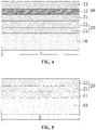
FIG. 4 is a structural schematic diagram of all film layers corresponding to a first region after a portion of a first diffusion film layer is removed according to an embodiment of the disclosure; -
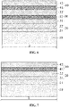
FIG. 5 is a schematic structural diagram of all film layers corresponding to a second region after a portion of a first diffusion film layer is removed according to an embodiment of the disclosure; -
FIG. 6 is a schematic structural diagram of all film layers corresponding to a first region after a second diffusion film layer is formed according to an embodiment of the disclosure; -
FIG. 7 is a schematic structural diagram of all film layers corresponding to a second region after a second diffusion film layer is formed according to an embodiment of the disclosure; -
FIG. 8 is a structural schematic diagram of all film layers corresponding to a first region after a portion of a second diffusion film layer is removed according to an embodiment of the disclosure; -
FIG. 9 is a schematic structural diagram of all film layers corresponding to a second region after a portion of a second diffusion film layer is removed according to an embodiment of the disclosure. -
- 10: substrate; 11: epitaxial layer;
- 20: dielectric layer; 21: second dielectric layer;
- 22: first dielectric layer; 30: first diffusion film layer;
- 31: barrier layer; 32: first metal oxide layer;
- 33: first sealing layer; 40: second diffusion film layer;
- 41: second metal oxide layer; 42: second sealing layer;
- A: first region; B: second region.
- To describe the purpose, the technical solutions and the advantages of embodiments of the disclosure more clearly, the technical solutions in the embodiments of the disclosure are described more clearly and integrally by combining the accompanying drawings in the embodiments of the disclosure. Apparently, the described embodiments are some of the embodiments of the disclosure, but not all the embodiments. Based on the embodiments of the disclosure, all other embodiments obtained by persons of ordinary skill in the art without involving an inventive effort shall fall within the scope of protection of the disclosure.
- In the related art, when a semiconductor structure is formed, a dielectric layer and a second diffusion film layer are sequentially formed on a substrate, the second diffusion film layer including a second metal oxide layer; then, the second diffusion film layer corresponding to a first region of the substrate is removed; then, a first diffusion film layer is formed on the dielectric layer corresponding to the first region, the first diffusion film layer including a first metal oxide layer; and next, annealing treatment is performed, so that a first metal element in the first metal oxide layer is diffused into the dielectric layer of the first region. However, the second diffusion film layer has a large diffusion inhibition effect on a second metal element in the second metal oxide layer, and the second metal element is not easy to diffuse into the dielectric layer corresponding to a second region, thereby resulting in poor performance of the semiconductor structure.
- In order to improve the performance of the semiconductor structure, the embodiments of the disclosure provide a manufacturing method for a semiconductor structure, including: sequentially forming a dielectric layer and a first diffusion film layer on a substrate, the first diffusion film layer including a first metal oxide layer; then, retaining the first diffusion film layer corresponding to a first region of the substrate, and removing the first diffusion film layer corresponding to a second region of the substrate; and next, forming the second diffusion film layer on the dielectric layer corresponding to the second region of the substrate. A second metal oxide layer in the second diffusion film layer interfaces with the dielectric layer, so that a second metal element in the second metal oxide layer is easy to diffuse into the corresponding dielectric layer during annealing treatment, thereby improving the performance of the semiconductor structure.
- Referring to
FIG. 1 to FIG. 9 ,FIG. 1 is a flowchart of a manufacturing method for a semiconductor structure according to an embodiment of the disclosure, which is used for forming a semiconductor structure having good performance.FIG. 2 to FIG. 9 are schematic structural diagrams of a semiconductor structure at different phases. The manufacturing method for a semiconductor structure is described below in combination withFIG. 1 to FIG. 9 . The manufacturing method for a semiconductor structure includes the following steps. - In S101, a substrate is provided, the substrate including a first region and a second region disposed outside the first region.
- Referring to
FIG. 2 and FIG. 3 , thesubstrate 10 in this embodiment of the disclosure includes the first region and the second region disposed outside the first region. Exemplarily, a gap is formed between the first region and the second region, the first region is A shown inFIG. 2 , and the second region is the B shown inFIG. 3 . - A transistor or other component is formed on the first region and the second region of the
substrate 10. Exemplarily, a Metal Oxide Semiconductor (MOS) transistor is formed in both the first region and the second region. - For convenience of description, in this embodiment of the disclosure and the following embodiments, description is made by taking forming an N-type transistor (NMOS) on the first region and forming a P-type transistor (PMOS) on the second region as an example.
- The
substrate 10 may be a semiconductor substrate. In this embodiment of the disclosure, thesubstrate 10 may be a silicon (Si) substrate. Of course, this embodiment of the disclosure is not limited thereto. Thesubstrate 10 in this embodiment of the disclosure may also include a germanium (Ge) substrate, a Silicon on Insulator (SOI) substrate, a silicon germanium (SiGe) substrate, a silicon carbide (SiC) substrate, or a gallium nitride (GaN) substrate, etc. - It is to be noted that before performing the subsequent steps, the manufacturing method for a semiconductor structure in this embodiment of the disclosure further includes: forming an
epitaxial layer 11 containing a preset metal on thesubstrate 10 corresponding to the second region. - Exemplarily, when the
substrate 10 is asilicon substrate 10, the preset metal may be germanium, and a silicon germanium layer may be formed on a portion of thesubstrate 10 by epitaxial growth or the like. As shown inFIG. 3 , theepitaxial layer 11 is disposed on the second region of thesubstrate 10. - It is to be noted that the material of the
epitaxial layer 11 may be the same as that of the substrate or different from that of the substrate, and the preset metal may also be other metals. This embodiment of the disclosure is not limited thereto. - In S102, a dielectric layer is formed on the substrate.
- Referring to
FIG. 2 and FIG. 3 , thedielectric layer 20 may be formed on thesubstrate 10 by a Chemical Vapor Deposition (CVD) process, a Physical Vapor Deposition (PVD) process, or an Atomic Layer Deposition (ALD) process. - As shown in
FIG. 2 and FIG. 3 , thedielectric layer 20 covers the first region and the second region of thesubstrate 10. In this embodiment of the disclosure, thedielectric layer 20 includes afirst dielectric layer 22 and asecond dielectric layer 21, and thesecond dielectric layer 21 is closer to thesubstrate 10 than thefirst dielectric layer 22. - The
second dielectric layer 21 may be an oxide layer, for example, the material of thesecond dielectric layer 21 may include silicon oxide and silicon oxynitride; and thefirst dielectric layer 22 may have a high-k, for example, the material of thefirst dielectric layer 22 may include hafnium oxide, silicon-doped hafnium oxide, silicon-doped zirconium oxide, etc. In this embodiment of the disclosure, the dielectric constant of thefirst dielectric layer 22 is greater than the dielectric constant of thesecond dielectric layer 21. - It is to be noted that the
second dielectric layer 21 corresponding to the second region may be doped with metal. Exemplarily, thesecond dielectric layer 21 may be made of germanium-doped silicon oxide, and the metal doped in thesecond dielectric layer 21 may be a preset metal or another metal. - In S103, a first diffusion film layer is formed on the dielectric layer, and the first diffusion film layer includes a first metal oxide layer.
- With continued reference to
FIG. 2 and FIG. 3 , in this embodiment of the disclosure, the firstdiffusion film layer 30 may be formed on thedielectric layer 20 by a deposition process, and the firstdiffusion film layer 30 covers thedielectric layer 20 corresponding to the first region and the second region. The firstdiffusion film layer 30 includes the firstmetal oxide layer 32, so that a first metal element in the firstmetal oxide layer 32 diffuses into thedielectric layer 20 corresponding to the first region during subsequent processing. Exemplarily, the first metal oxide layer may be made of lanthanum oxide (La203). - In S104, the first diffusion film layer corresponding to the second region is removed.
- Referring to
FIG. 4 and FIG. 5 , the firstdiffusion film layer 30 may be removed by an etching process, such as dry etching or wet etching. In this step, a portion of the firstdiffusion film layer 30 is removed. As shown inFIG. 4 and FIG. 5 , the firstdiffusion film layer 30 corresponding to the second region is removed, and the firstdiffusion film layer 30 corresponding to the first region is retained. - In S105, a second diffusion film layer is formed on the dielectric layer corresponding to the second region, and the second diffusion film layer includes a second metal oxide layer interfacing with the dielectric layer.
- Referring to
FIG. 6 and FIG. 7 , the seconddiffusion film layer 40 may be formed on thedielectric layer 20 corresponding to the second region by a deposition process, and the secondmetal oxide layer 41 in the seconddiffusion film layer 40 interfaces with thedielectric layer 20. Exemplarily, the second metal oxide layer may be made of aluminum oxide (A1203). - In some possible examples, the step of forming a second
diffusion film layer 40 on thedielectric layer 20 corresponding to the second region includes: - first, forming the second
diffusion film layer 40 on the firstdiffusion film layer 30 corresponding to the first region and thedielectric layer 20 corresponding to the second region. As shown inFIG. 6 and FIG. 7 , the seconddiffusion film layer 40 covers the firstdiffusion film layer 30 and thedielectric layer 20, i.e., the seconddiffusion film layer 40 is deposited simultaneously on thedielectric layer 20 corresponding to the first region and the second region. - It is to be noted that the second
diffusion film layer 40 includes the secondmetal oxide layer 41. As shown inFIG. 6 and FIG. 7 , the secondmetal oxide layer 41 interfaces with the firstdiffusion film layer 30 corresponding to the first region, and thedielectric layer 20 corresponding to the second region. - After the second
diffusion film layer 40 is formed, as shown inFIG. 6 , thedielectric layer 20, the firstdiffusion film layer 30, and the seconddiffusion film layer 40 are sequentially formed on the first region of thesubstrate 10 from bottom to top; and as shown inFIG. 7 , thedielectric layer 20 and the seconddiffusion film layer 40 are sequentially formed on the second region of thesubstrate 10 from bottom to top. - Then, the second
diffusion film layer 40 corresponding to the first region is removed by etching. That is to say, the seconddiffusion film layer 40 corresponding to the second region is retained. Referring toFIG. 8 and FIG. 9 , the firstdiffusion film layer 30 is formed on thedielectric layer 20 corresponding to the first region, and the seconddiffusion film layer 40 is formed on thedielectric layer 20 corresponding to the second region. - In S106, annealing treatment is performed to diffuse a first metal element in the first metal oxide layer into the dielectric layer corresponding to the first region and diffuse a second metal element in the second metal oxide layer into the dielectric layer corresponding to the second region.
- During annealing, since the second
metal oxide layer 41 interfaces with thedielectric layer 20, i.e., as shown inFIG. 9 , the secondmetal oxide layer 41 is in contact with thedielectric layer 20, and no other film layer is blocked between the secondmetal oxide layer 41 and thedielectric layer 20, the second metal in the secondmetal oxide layer 41 is easy to diffuse into thedielectric layer 20 corresponding to the second region, thereby improving the performance of the semiconductor structure. - The manufacturing method for a semiconductor structure provided in this embodiment of the disclosure includes: the
substrate 10 is provided firstly, thesubstrate 10 including the first region and the second region disposed outside the first region; secondly, thedielectric layer 20 is formed on thesubstrate 10; thirdly, the firstdiffusion film layer 30 is formed on thedielectric layer 20, the firstdiffusion film layer 30 including the firstmetal oxide layer 32; fourthly, the firstdiffusion film layer 30 corresponding to the second region is removed; fifthly, the seconddiffusion film layer 40 is formed on thedielectric layer 20 corresponding to the second region, the seconddiffusion film layer 40 including the secondmetal oxide layer 41 interfacing with thedielectric layer 20; and sixthly, annealing treatment is performed to diffuse the first metal element in the firstmetal oxide layer 32 into thedielectric layer 20 corresponding to the first region and diffuse the second metal element in the secondmetal oxide layer 41 into thedielectric layer 20 corresponding to the second region. Since the secondmetal oxide layer 41 interfaces with thedielectric layer 20, and no other film layer is blocked therebetween, the second metal in the secondmetal oxide layer 41 is easier to diffuse into thedielectric layer 20 corresponding to the second region, thereby improving the performance of the formed semiconductor structure. - It is to be noted that referring to
FIG. 2 and FIG. 3 , the firstdiffusion film layer 30 includes the firstmetal oxide layer 32 and afirst sealing layer 33. Thefirst sealing layer 33 is disposed on a side of the firstmetal oxide layer 32 facing away from thesubstrate 10. Thefirst sealing layer 33 may protect the first metal oxide layer. Exemplarily, thefirst sealing layer 33 may be made of titanium nitride (TiN). - The step of forming a first
diffusion film layer 30 includes: sequentially forming the firstmetal oxide layer 32 and thefirst sealing layer 33 on thedielectric layer 20. That is to say, the firstmetal oxide layer 32 is first formed on thedielectric layer 20, and then thefirst sealing layer 33 is formed on the firstmetal oxide layer 32. - Before forming the first
metal oxide layer 32, the manufacturing method for a semiconductor structure in this embodiment of the disclosure further includes: forming abarrier layer 31 on thedielectric layer 20. - The
barrier layer 31 may be used to prevent damage to thedielectric layer 20 when the firstdiffusion film layer 30 is subsequently removed. Exemplarily, when the firstdiffusion film layer 30 is removed by an etching process, thebarrier layer 31 may serve as an etch stop layer, for example, thebarrier layer 31 may be a titanium nitride layer. - It is to be noted that referring to
FIG. 6 and FIG. 7 , when the firstdiffusion film layer 30 includes thebarrier layer 31, the firstmetal oxide layer 32, and thefirst sealing layer 33 which are sequentially stacked, thefirst sealing layer 33 is disposed on a side of the firstmetal oxide layer 32 facing away from thesubstrate 10. The step of forming a seconddiffusion film layer 40 on the firstdiffusion film layer 30 corresponding to the first region and thedielectric layer 20 corresponding to the second region includes: - sequentially forming the second
metal oxide layer 41 and asecond sealing layer 42 on the firstdiffusion film layer 30 corresponding to the first region and thedielectric layer 20 corresponding to the second region. As shown inFIG. 7 andFIG. 8 , the seconddiffusion film layer 40 includes the secondmetal oxide layer 41 and thesecond sealing layer 42 disposed on the secondmetal oxide layer 41. Thesecond sealing layer 42 may protect the secondmetal oxide layer 41, and thesecond sealing layer 42 may be made of titanium nitride. - This embodiment of the disclosure provides a semiconductor structure. Referring to
FIG. 8 and FIG. 9 , the semiconductor structure includes asubstrate 10 and adielectric layer 20 disposed on thesubstrate 10. Thesubstrate 10 includes a first region and a second region disposed outside the first region. Exemplarily, a gap is formed between the first region and the second region, the first region is A shown inFIG. 8 , and the second region is the B shown inFIG. 9 . - The
substrate 10 may be a semiconductor substrate. Exemplarily, thesubstrate 10 may be a silicon (Si) substrate. Of course, this embodiment of the disclosure is not limited thereto. The substrate in this embodiment of the disclosure may also be made of other materials. - In some possible examples, an
epitaxial layer 11 is provided on thesubstrate 10 of the second region, theepitaxial layer 11 includes a preset metal, and the preset metal may be germanium. As shown inFIG. 9 , theepitaxial layer 11 is formed on thesubstrate 10 corresponding to the second region, for example, a silicon germanium layer may be formed on thesubstrate 10 corresponding to the second region by epitaxial growth or the like. - It is to be noted that the material of the
epitaxial layer 11 may be the same as that of the substrate or different from that of the substrate, and the preset metal may also be other metals. This embodiment of the disclosure is not limited thereto. - With continued reference to
FIG. 8 and FIG. 9 , thedielectric layer 20 covers the first region and the second region of thesubstrate 10. In this embodiment of the disclosure, thedielectric layer 20 includes afirst dielectric layer 22 and asecond dielectric layer 21 which are stacked, and thesecond dielectric layer 21 is closer to thesubstrate 10 than thefirst dielectric layer 22, i.e., thefirst dielectric layer 22 is disposed on a side of thesecond dielectric layer 21 facing away from thesubstrate 10. - The
second dielectric layer 21 may be an oxide layer, for example, the material of thesecond dielectric layer 21 may include silicon oxide or silicon oxynitride; and thefirst dielectric layer 22 may have a high-k, for example, the material of thefirst dielectric layer 22 may include hafnium oxide, silicon-doped hafnium oxide, silicon-doped zirconium oxide, etc. The dielectric constant of thefirst dielectric layer 22 is greater than the dielectric constant of thesecond dielectric layer 21. - It is to be noted that the
second dielectric layer 21 corresponding to the second region may be doped with metal. Exemplarily, thesecond dielectric layer 21 may be made of germanium-doped silicon oxide, and the metal doped in thesecond dielectric layer 21 may be a preset metal or other metals. - With continued reference to
FIG. 8 and FIG. 9 , the semiconductor structure further includes a firstdiffusion film layer 30 and a seconddiffusion film layer 40. As shown inFIG. 8 , the firstdiffusion film layer 30 is formed on thedielectric layer 20 corresponding to the first region, and as shown inFIG. 9 , the seconddiffusion film layer 40 is formed on thedielectric layer 20 corresponding to the second region. - The first
diffusion film layer 30 includes a firstmetal oxide layer 32, and a first metal element in the layer may diffuse into thedielectric layer 20 corresponding to the first region during annealing treatment. Exemplarily, the first metal oxide layer may be made of lanthanum oxide (La203). - In some possible examples, the first
diffusion film layer 30 includes the firstmetal oxide layer 32 and afirst sealing layer 33 which are stacked. Thefirst sealing layer 33 is disposed on a side of the firstmetal oxide layer 32 facing away from thesubstrate 10. Thefirst sealing layer 33 may protect the first metal oxide layer. Exemplarily, thefirst sealing layer 33 may be made of titanium nitride. - It is to be noted that the first
diffusion film layer 30 further includes abarrier layer 31 disposed between the firstmetal oxide layer 32 and thedielectric layer 20, and thebarrier layer 31 may protect thedielectric layer 20 to reduce or avoid damage to thedielectric layer 20. When the first metal oxide layer is made of lanthanum oxide, and thebarrier layer 31 may be made of titanium nitride. - The second
diffusion film layer 40 includes a secondmetal oxide layer 41. The secondmetal oxide layer 41 interfaces with thedielectric layer 20, i.e., the secondmetal oxide layer 41 is in contact with thedielectric layer 20, and no other film layer is blocked between the two layers, so that the second metal element in the secondmetal oxide layer 41 is easy to diffuse into thedielectric layer 20 corresponding to the second region during annealing treatment. - In some possible examples, the second
diffusion film layer 40 further includes asecond sealing layer 42. Thesecond sealing layer 42 is disposed on a side of the secondmetal oxide layer 41 facing away from thesubstrate 10. As shown inFIG. 9 , thesecond sealing layer 42 is disposed above the secondmetal oxide layer 41. Thesecond sealing layer 42 may protect the second metal oxide layer. Exemplarily, thesecond sealing layer 42 may be made of titanium nitride. - With continued reference to
FIG. 8 and FIG. 9 , in this embodiment of the disclosure, the film layers disposed above thesubstrate 10 and corresponding to the first region may form an N-type transistor, and the film layers disposed above thesubstrate 10 and corresponding to the second region may form a P-type transistor. - The semiconductor structure provided in this embodiment of the disclosure includes the
substrate 10 and thedielectric layer 20 provided on thesubstrate 10; thesubstrate 10 includes the first region and the second region disposed outside the first region; and the seconddiffusion film layer 40 is provided on thedielectric layer 20 corresponding to the second region, and the seconddiffusion film layer 40 includes the secondmetal oxide layer 41 interfacing with thedielectric layer 20. Since the secondmetal oxide layer 41 interfaces with thedielectric layer 20, and no other film layer blocks the second metal element in the secondmetal oxide layer 41, the second metal element is easy to diffuse into thedielectric layer 20 corresponding to the second region, thereby improving the performance of the semiconductor structure. - The embodiments or implementations of the present description are described in a progressive manner, and each embodiment focuses on illustrating differences from one another. Mutual references may be made to the same or similar portions among these embodiments.
- Persons of ordinary skill in the art should understand that, in the disclosure of the disclosure, terms of "longitudinal", "lateral", "upper", "front", "back", "left", "right", "perpendicular", "horizontal", "top", "bottom", "inner", "outer", etc. that indicate relations of directions or positions are based on the relations of directions or positions shown in the appended drawings, which are only to facilitate description of the disclosure and to simplify the description, rather than to indicate or imply that the referred system or element is limited to the specific direction or to be operated or configured in the specific direction. Therefore, the above-mentioned terms shall not be interpreted as limitation to the disclosure.
- In the description of the present description, the description with reference to the terms "one embodiment", "some embodiments", "illustrative embodiment", "example", "specific example", or "some examples", or the like, means that specific features, structures, materials or characteristics described in conjunction with the embodiments or the examples are included in the at least one embodiment or example of the disclosure. In the present description, the illustrative expressions of the above terms do not necessarily refer to the same embodiment or example. Moreover, the described specific features, structures, materials or characteristics can be combined in a proper manner in any one of or more embodiments or examples.
- It is to be explained at last that: the foregoing embodiments are merely intended for describing the technical solutions of the disclosure other than limiting the disclosure. Although the disclosure is described in detail with reference to the foregoing embodiments, persons of ordinary skill in the art should understand that they may still make modifications to the technical solutions described in the foregoing embodiments or make equivalent replacements to some or all technical features thereof, and such modifications or replacements do not depart the essence of the corresponding technical solutions from the scope of the technical solutions of the embodiments of the disclosure.
Claims (15)
- A manufacturing method for a semiconductor structure, comprising:providing a substrate, the substrate comprising a first region and a second region disposed outside the first region;forming a dielectric layer on the substrate;forming a first diffusion film layer on the dielectric layer, the first diffusion film layer comprising a first metal oxide layer;removing the first diffusion film layer corresponding to the second region;forming a second diffusion film layer on the dielectric layer corresponding to the second region, the second diffusion film layer comprising a second metal oxide layer interfacing with the dielectric layer; andperforming annealing treatment to diffuse a first metal element in the first metal oxide layer into the dielectric layer corresponding to the first region and diffuse a second metal element in the second metal oxide layer into the dielectric layer corresponding to the second region.
- The manufacturing method for a semiconductor structure of claim 1, wherein
forming the first diffusion film layer comprises:
sequentially forming the first metal oxide layer and a first sealing layer on the dielectric layer. - The manufacturing method for a semiconductor structure of claim 2, further comprising: before forming the first metal oxide layer, forming a barrier layer on the dielectric layer.
- The manufacturing method for a semiconductor structure of claim 3, wherein forming the second diffusion film layer on the dielectric layer corresponding to the second region comprises:forming the second diffusion film layer on the first diffusion film layer corresponding to the first region and the dielectric layer corresponding to the second region; andremoving the second diffusion film layer corresponding to the first region by etching.
- The manufacturing method for a semiconductor structure of claim 2, wherein forming the second diffusion film layer on the first diffusion film layer corresponding to the first region and the dielectric layer corresponding to the second region comprises:
sequentially forming the second metal oxide layer and a second sealing layer on the first diffusion film layer corresponding to the first region and the dielectric layer corresponding to the second region. - The manufacturing method for a semiconductor structure of claim 1, further comprising: before forming the dielectric layer,
forming an epitaxial layer containing a preset metal on the substrate corresponding to the second region. - The manufacturing method for a semiconductor structure of claim 6, wherein the substrate is a silicon substrate, and the preset metal is germanium.
- A semiconductor structure, comprising: a substrate, the substrate having a first region and a second region disposed outside the first region,
wherein the semiconductor structure further comprises a dielectric layer provided on the substrate, wherein a first diffusion film layer is provided on the dielectric layer corresponding to the first region, the first diffusion film layer comprising a first metal oxide layer; and a second diffusion film layer is provided on the dielectric layer corresponding to the second region, the second diffusion film layer comprising a second metal oxide layer interfacing with the dielectric layer. - The semiconductor structure of claim 8, wherein the first diffusion film layer comprises the first metal oxide layer and a first sealing layer which are stacked, and the first sealing layer is disposed on a side of the first metal oxide layer facing away from the substrate.
- The semiconductor structure of claim 9, wherein the first diffusion film layer further comprises a barrier layer disposed between the first metal oxide layer and the dielectric layer.
- The semiconductor structure of claim 8, wherein the second diffusion film layer further comprises a second sealing layer disposed on a side of the second metal oxide layer facing away from the substrate.
- The semiconductor structure of claim 8, wherein an epitaxial layer containing a preset metal is provided on the substrate corresponding to the second region.
- The semiconductor structure of claim 12, wherein the substrate is a silicon substrate, and the preset metal is germanium.
- The semiconductor structure of claim 8, wherein the dielectric layer comprises a first dielectric layer and a second dielectric layer which are stacked, the first dielectric layer is disposed on a side of the second dielectric layer facing away from the substrate, and a dielectric constant of the first dielectric layer is greater than a dielectric constant of the second dielectric layer.
- The semiconductor structure of claim 8, wherein the film layers disposed on the substrate and corresponding to the first region form an N-type transistor, and the film layers disposed on the substrate and corresponding to the second region form a P-type transistor.
Applications Claiming Priority (2)
| Application Number | Priority Date | Filing Date | Title |
|---|---|---|---|
| CN202110032629.4A CN114765130A (en) | 2021-01-11 | 2021-01-11 | Semiconductor structure manufacturing method and semiconductor structure |
| PCT/CN2021/103732 WO2022147984A1 (en) | 2021-01-11 | 2021-06-30 | Method for manufacturing semiconductor structure, and semiconductor structure |
Publications (2)
| Publication Number | Publication Date |
|---|---|
| EP4053891A1 true EP4053891A1 (en) | 2022-09-07 |
| EP4053891A4 EP4053891A4 (en) | 2023-01-04 |
Family
ID=82322050
Family Applications (1)
| Application Number | Title | Priority Date | Filing Date |
|---|---|---|---|
| EP21878741.4A Withdrawn EP4053891A4 (en) | 2021-01-11 | 2021-06-30 | METHOD FOR FABRICATING A SEMICONDUCTOR STRUCTURE, AND SEMICONDUCTOR STRUCTURE |
Country Status (2)
| Country | Link |
|---|---|
| US (1) | US12148619B2 (en) |
| EP (1) | EP4053891A4 (en) |
Family Cites Families (15)
| Publication number | Priority date | Publication date | Assignee | Title |
|---|---|---|---|---|
| US8021939B2 (en) | 2007-12-12 | 2011-09-20 | International Business Machines Corporation | High-k dielectric and metal gate stack with minimal overlap with isolation region and related methods |
| US8017469B2 (en) | 2009-01-21 | 2011-09-13 | Freescale Semiconductor, Inc. | Dual high-k oxides with sige channel |
| US7838908B2 (en) | 2009-01-26 | 2010-11-23 | International Business Machines Corporation | Semiconductor device having dual metal gates and method of manufacture |
| US8309419B2 (en) * | 2009-02-04 | 2012-11-13 | Freescale Semiconductor, Inc. | CMOS integration with metal gate and doped high-K oxides |
| US8232154B2 (en) | 2009-09-21 | 2012-07-31 | United Microelectronics Corp. | Method for fabricating semiconductor device |
| FR2952225B1 (en) | 2009-11-03 | 2012-03-23 | St Microelectronics Sa | METHOD FOR FORMING A SILICON-GERMANIUM CHANNEL MOS TRANSISTOR |
| JP2011187478A (en) * | 2010-03-04 | 2011-09-22 | Toshiba Corp | Semiconductor device and method of manufacturing the same |
| US8941184B2 (en) | 2011-12-16 | 2015-01-27 | International Business Machines Corporation | Low threshold voltage CMOS device |
| KR20130127257A (en) | 2012-05-14 | 2013-11-22 | 삼성전자주식회사 | Semiconductor device and method for manufacturing the device |
| EP2717308A1 (en) | 2012-10-08 | 2014-04-09 | Imec | A method for manufacturing a dual work function semiconductor device |
| CN105448831A (en) | 2014-08-05 | 2016-03-30 | 中芯国际集成电路制造(上海)有限公司 | High-K metal gate CMOS device and forming method thereof |
| CN105529327B (en) | 2014-10-22 | 2019-03-15 | 中国科学院微电子研究所 | CMOS device and method of making the same |
| CN109786448A (en) | 2017-11-10 | 2019-05-21 | 中芯国际集成电路制造(上海)有限公司 | Metal gates, semiconductor devices and its manufacturing method |
| US11862516B2 (en) * | 2020-10-15 | 2024-01-02 | Changxin Memory Technologies, Inc. | Semiconductor structure manufacturing method |
| EP4160664A4 (en) * | 2021-08-20 | 2023-04-05 | Changxin Memory Technologies, Inc. | SEMICONDUCTOR STRUCTURE AND METHOD OF MANUFACTURING THEREOF |
-
2021
- 2021-06-30 EP EP21878741.4A patent/EP4053891A4/en not_active Withdrawn
- 2021-10-20 US US17/505,678 patent/US12148619B2/en active Active
Also Published As
| Publication number | Publication date |
|---|---|
| US20220223420A1 (en) | 2022-07-14 |
| US12148619B2 (en) | 2024-11-19 |
| EP4053891A4 (en) | 2023-01-04 |
Similar Documents
| Publication | Publication Date | Title |
|---|---|---|
| US12266711B2 (en) | Semiconductor device and method for fabricating the same | |
| US9082853B2 (en) | Bulk finFET with punchthrough stopper region and method of fabrication | |
| US10211309B2 (en) | Method and device for metal gate stacks | |
| US9236263B2 (en) | Method for fabricating semiconductor device including silicon-containing layer and metal-containing layer, and conductive structure of the same | |
| US8673758B2 (en) | Structure of metal gate and fabrication method thereof | |
| CN101661883B (en) | Manufacturing method of semiconductor element | |
| US10692779B2 (en) | Method and structure for CMOS metal gate stack | |
| US9105623B2 (en) | Semiconductor device having metal gate and manufacturing method thereof | |
| CN102110650A (en) | Semiconductor device and manufacturing method thereof | |
| US8324118B2 (en) | Manufacturing method of metal gate structure | |
| US9478627B2 (en) | Semiconductor structure and process thereof | |
| US20110215413A1 (en) | Semiconductor device and method for manufacturing the same | |
| US8921171B2 (en) | Method for forming gate structure, method for forming semiconductor device, and semiconductor device | |
| CN109786448A (en) | Metal gates, semiconductor devices and its manufacturing method | |
| US9318390B2 (en) | CMOS circuit and method for fabricating the same | |
| US8975666B2 (en) | MOS transistor and process thereof | |
| US12125909B2 (en) | Asymmetric semiconductor device including LDD region and manufacturing method thereof | |
| CN106328529B (en) | MOS transistor and method of forming the same | |
| US7498626B2 (en) | Semiconductor device and method of manufacturing the same | |
| US12148619B2 (en) | Manufacturing method for semiconductor structure, and semiconductor structure | |
| US9449829B1 (en) | Semiconductor process | |
| CN103137456A (en) | Manufacturing method for P-channel metal oxide semiconductor (PMOS) transistor metal grid | |
| US10651285B2 (en) | Method for avoiding IL regrown in a HKMG process | |
| WO2022147984A1 (en) | Method for manufacturing semiconductor structure, and semiconductor structure | |
| CN115295623A (en) | Semiconductor device and method for manufacturing the same |
Legal Events
| Date | Code | Title | Description |
|---|---|---|---|
| STAA | Information on the status of an ep patent application or granted ep patent |
Free format text: STATUS: UNKNOWN |
|
| STAA | Information on the status of an ep patent application or granted ep patent |
Free format text: STATUS: THE INTERNATIONAL PUBLICATION HAS BEEN MADE |
|
| PUAI | Public reference made under article 153(3) epc to a published international application that has entered the european phase |
Free format text: ORIGINAL CODE: 0009012 |
|
| STAA | Information on the status of an ep patent application or granted ep patent |
Free format text: STATUS: REQUEST FOR EXAMINATION WAS MADE |
|
| 17P | Request for examination filed |
Effective date: 20220419 |
|
| AK | Designated contracting states |
Kind code of ref document: A1 Designated state(s): AL AT BE BG CH CY CZ DE DK EE ES FI FR GB GR HR HU IE IS IT LI LT LU LV MC MK MT NL NO PL PT RO RS SE SI SK SM TR |
|
| A4 | Supplementary search report drawn up and despatched |
Effective date: 20221202 |
|
| RIC1 | Information provided on ipc code assigned before grant |
Ipc: H01L 27/092 20060101ALI20221128BHEP Ipc: H01L 21/28 20060101ALI20221128BHEP Ipc: H01L 21/8238 20060101AFI20221128BHEP |
|
| DAV | Request for validation of the european patent (deleted) | ||
| DAX | Request for extension of the european patent (deleted) | ||
| STAA | Information on the status of an ep patent application or granted ep patent |
Free format text: STATUS: EXAMINATION IS IN PROGRESS |
|
| 17Q | First examination report despatched |
Effective date: 20250507 |
|
| STAA | Information on the status of an ep patent application or granted ep patent |
Free format text: STATUS: THE APPLICATION HAS BEEN WITHDRAWN |
|
| 18W | Application withdrawn |
Effective date: 20250905 |