EP4053879A1 - Deposition of highly crystalline 2d materials - Google Patents
Deposition of highly crystalline 2d materials Download PDFInfo
- Publication number
- EP4053879A1 EP4053879A1 EP21159840.4A EP21159840A EP4053879A1 EP 4053879 A1 EP4053879 A1 EP 4053879A1 EP 21159840 A EP21159840 A EP 21159840A EP 4053879 A1 EP4053879 A1 EP 4053879A1
- Authority
- EP
- European Patent Office
- Prior art keywords
- etching
- substrate
- transition metal
- film
- mos
- Prior art date
- Legal status (The legal status is an assumption and is not a legal conclusion. Google has not performed a legal analysis and makes no representation as to the accuracy of the status listed.)
- Pending
Links
Images




Classifications
-
- H—ELECTRICITY
- H10—SEMICONDUCTOR DEVICES; ELECTRIC SOLID-STATE DEVICES NOT OTHERWISE PROVIDED FOR
- H10P—GENERIC PROCESSES OR APPARATUS FOR THE MANUFACTURE OR TREATMENT OF DEVICES COVERED BY CLASS H10
- H10P14/00—Formation of materials, e.g. in the shape of layers or pillars
- H10P14/20—Formation of materials, e.g. in the shape of layers or pillars of semiconductor materials
- H10P14/24—Formation of materials, e.g. in the shape of layers or pillars of semiconductor materials using chemical vapour deposition [CVD]
-
- H—ELECTRICITY
- H10—SEMICONDUCTOR DEVICES; ELECTRIC SOLID-STATE DEVICES NOT OTHERWISE PROVIDED FOR
- H10D—INORGANIC ELECTRIC SEMICONDUCTOR DEVICES
- H10D30/00—Field-effect transistors [FET]
- H10D30/01—Manufacture or treatment
- H10D30/021—Manufacture or treatment of FETs having insulated gates [IGFET]
- H10D30/027—Manufacture or treatment of FETs having insulated gates [IGFET] of lateral single-gate IGFETs
-
- H—ELECTRICITY
- H10—SEMICONDUCTOR DEVICES; ELECTRIC SOLID-STATE DEVICES NOT OTHERWISE PROVIDED FOR
- H10D—INORGANIC ELECTRIC SEMICONDUCTOR DEVICES
- H10D62/00—Semiconductor bodies, or regions thereof, of devices having potential barriers
- H10D62/80—Semiconductor bodies, or regions thereof, of devices having potential barriers characterised by the materials
- H10D62/82—Heterojunctions
- H10D62/8281—Heterojunctions comprising only transition metal dichalcogenide materials heterojunctions, e.g. MoS2/WSe2
-
- H—ELECTRICITY
- H10—SEMICONDUCTOR DEVICES; ELECTRIC SOLID-STATE DEVICES NOT OTHERWISE PROVIDED FOR
- H10D—INORGANIC ELECTRIC SEMICONDUCTOR DEVICES
- H10D62/00—Semiconductor bodies, or regions thereof, of devices having potential barriers
- H10D62/80—Semiconductor bodies, or regions thereof, of devices having potential barriers characterised by the materials
- H10D62/881—Semiconductor bodies, or regions thereof, of devices having potential barriers characterised by the materials being a two-dimensional material
- H10D62/883—Transition metal dichalcogenides, e.g. MoSe2
-
- H—ELECTRICITY
- H10—SEMICONDUCTOR DEVICES; ELECTRIC SOLID-STATE DEVICES NOT OTHERWISE PROVIDED FOR
- H10D—INORGANIC ELECTRIC SEMICONDUCTOR DEVICES
- H10D99/00—Subject matter not provided for in other groups of this subclass
-
- H—ELECTRICITY
- H10—SEMICONDUCTOR DEVICES; ELECTRIC SOLID-STATE DEVICES NOT OTHERWISE PROVIDED FOR
- H10P—GENERIC PROCESSES OR APPARATUS FOR THE MANUFACTURE OR TREATMENT OF DEVICES COVERED BY CLASS H10
- H10P14/00—Formation of materials, e.g. in the shape of layers or pillars
- H10P14/20—Formation of materials, e.g. in the shape of layers or pillars of semiconductor materials
- H10P14/27—Formation of materials, e.g. in the shape of layers or pillars of semiconductor materials using selective deposition, e.g. simultaneous growth of monocrystalline and non-monocrystalline semiconductor materials
- H10P14/271—Formation of materials, e.g. in the shape of layers or pillars of semiconductor materials using selective deposition, e.g. simultaneous growth of monocrystalline and non-monocrystalline semiconductor materials characterised by the preparation of substrate for selective deposition
- H10P14/274—Formation of materials, e.g. in the shape of layers or pillars of semiconductor materials using selective deposition, e.g. simultaneous growth of monocrystalline and non-monocrystalline semiconductor materials characterised by the preparation of substrate for selective deposition using seed materials
-
- H—ELECTRICITY
- H10—SEMICONDUCTOR DEVICES; ELECTRIC SOLID-STATE DEVICES NOT OTHERWISE PROVIDED FOR
- H10P—GENERIC PROCESSES OR APPARATUS FOR THE MANUFACTURE OR TREATMENT OF DEVICES COVERED BY CLASS H10
- H10P14/00—Formation of materials, e.g. in the shape of layers or pillars
- H10P14/20—Formation of materials, e.g. in the shape of layers or pillars of semiconductor materials
- H10P14/29—Formation of materials, e.g. in the shape of layers or pillars of semiconductor materials characterised by the substrates
- H10P14/2901—Materials
- H10P14/2922—Materials being non-crystalline insulating materials, e.g. glass or polymers
-
- H—ELECTRICITY
- H10—SEMICONDUCTOR DEVICES; ELECTRIC SOLID-STATE DEVICES NOT OTHERWISE PROVIDED FOR
- H10P—GENERIC PROCESSES OR APPARATUS FOR THE MANUFACTURE OR TREATMENT OF DEVICES COVERED BY CLASS H10
- H10P14/00—Formation of materials, e.g. in the shape of layers or pillars
- H10P14/20—Formation of materials, e.g. in the shape of layers or pillars of semiconductor materials
- H10P14/34—Deposited materials, e.g. layers
- H10P14/3402—Deposited materials, e.g. layers characterised by the chemical composition
- H10P14/3436—Deposited materials, e.g. layers characterised by the chemical composition being chalcogenide semiconductor materials not being oxides, e.g. ternary compounds
-
- H—ELECTRICITY
- H10—SEMICONDUCTOR DEVICES; ELECTRIC SOLID-STATE DEVICES NOT OTHERWISE PROVIDED FOR
- H10P—GENERIC PROCESSES OR APPARATUS FOR THE MANUFACTURE OR TREATMENT OF DEVICES COVERED BY CLASS H10
- H10P14/00—Formation of materials, e.g. in the shape of layers or pillars
- H10P14/20—Formation of materials, e.g. in the shape of layers or pillars of semiconductor materials
- H10P14/34—Deposited materials, e.g. layers
- H10P14/3451—Structure
- H10P14/3452—Microstructure
-
- H—ELECTRICITY
- H10—SEMICONDUCTOR DEVICES; ELECTRIC SOLID-STATE DEVICES NOT OTHERWISE PROVIDED FOR
- H10P—GENERIC PROCESSES OR APPARATUS FOR THE MANUFACTURE OR TREATMENT OF DEVICES COVERED BY CLASS H10
- H10P14/00—Formation of materials, e.g. in the shape of layers or pillars
- H10P14/20—Formation of materials, e.g. in the shape of layers or pillars of semiconductor materials
- H10P14/34—Deposited materials, e.g. layers
- H10P14/3451—Structure
- H10P14/3452—Microstructure
- H10P14/3458—Monocrystalline
-
- H—ELECTRICITY
- H10—SEMICONDUCTOR DEVICES; ELECTRIC SOLID-STATE DEVICES NOT OTHERWISE PROVIDED FOR
- H10P—GENERIC PROCESSES OR APPARATUS FOR THE MANUFACTURE OR TREATMENT OF DEVICES COVERED BY CLASS H10
- H10P14/00—Formation of materials, e.g. in the shape of layers or pillars
- H10P14/20—Formation of materials, e.g. in the shape of layers or pillars of semiconductor materials
- H10P14/38—Formation of materials, e.g. in the shape of layers or pillars of semiconductor materials characterised by treatments done after the formation of the materials
-
- H—ELECTRICITY
- H10—SEMICONDUCTOR DEVICES; ELECTRIC SOLID-STATE DEVICES NOT OTHERWISE PROVIDED FOR
- H10P—GENERIC PROCESSES OR APPARATUS FOR THE MANUFACTURE OR TREATMENT OF DEVICES COVERED BY CLASS H10
- H10P50/00—Etching of wafers, substrates or parts of devices
- H10P50/20—Dry etching; Plasma etching; Reactive-ion etching
-
- H—ELECTRICITY
- H10—SEMICONDUCTOR DEVICES; ELECTRIC SOLID-STATE DEVICES NOT OTHERWISE PROVIDED FOR
- H10P—GENERIC PROCESSES OR APPARATUS FOR THE MANUFACTURE OR TREATMENT OF DEVICES COVERED BY CLASS H10
- H10P52/00—Grinding, lapping or polishing of wafers, substrates or parts of devices
-
- H—ELECTRICITY
- H10—SEMICONDUCTOR DEVICES; ELECTRIC SOLID-STATE DEVICES NOT OTHERWISE PROVIDED FOR
- H10P—GENERIC PROCESSES OR APPARATUS FOR THE MANUFACTURE OR TREATMENT OF DEVICES COVERED BY CLASS H10
- H10P95/00—Generic processes or apparatus for manufacture or treatments not covered by the other groups of this subclass
- H10P95/70—Chemical treatments
-
- H—ELECTRICITY
- H10—SEMICONDUCTOR DEVICES; ELECTRIC SOLID-STATE DEVICES NOT OTHERWISE PROVIDED FOR
- H10D—INORGANIC ELECTRIC SEMICONDUCTOR DEVICES
- H10D62/00—Semiconductor bodies, or regions thereof, of devices having potential barriers
- H10D62/80—Semiconductor bodies, or regions thereof, of devices having potential barriers characterised by the materials
-
- H—ELECTRICITY
- H10—SEMICONDUCTOR DEVICES; ELECTRIC SOLID-STATE DEVICES NOT OTHERWISE PROVIDED FOR
- H10P—GENERIC PROCESSES OR APPARATUS FOR THE MANUFACTURE OR TREATMENT OF DEVICES COVERED BY CLASS H10
- H10P14/00—Formation of materials, e.g. in the shape of layers or pillars
- H10P14/20—Formation of materials, e.g. in the shape of layers or pillars of semiconductor materials
- H10P14/29—Formation of materials, e.g. in the shape of layers or pillars of semiconductor materials characterised by the substrates
- H10P14/2901—Materials
- H10P14/2921—Materials being crystalline insulating materials
Definitions
- the invention relates to the field of metal chalcogenide films. More specifically it relates to a method for forming providing a film of one or more monolayers of transition metal dichalcogenides on a substrate.
- MX 2 transition metal dichalcogenide
- the semiconducting group-VI MX 2 materials possess a layered crystal structure with layer-dependent physical and electrical properties, and a chemically inert surface free of dangling bonds.
- MX 2 materials complement Silicon as channel material in nanoelectronic devices with ultra-scaled channel thickness at excellent electrostatic gate control and anticipated absence of interface defects, and decreased off-state power consumption.
- their unique properties predominantly excel in one monolayer film and few monolayer film form, which fuels research on the large-area deposition of atomically thin MX 2 material.
- sequence of depositing/selectively removing is executed at least twice.
- the sequence may be executed until one or more closed monolayers are obtained.
- etchants used for the etching may be selected from the list of CI2, HCI, CO.
- the transition metal dichalcogenides are deposited by metal-organic chemical vapor deposition.
- a method, according to embodiments of the present invention, may be applied on any substrate, as long as the main growth mode of the MX 2 layer is planar, since it is based on the presence of dangling bonds on island edges, vs. a fully saturated basal plane surface.
- the substrate can for example be a sapphire substrate.
- the transition metal dichalcogenide is MoS 2 .
- the invention is, however, not limited thereto. Also other transition metal dichalcogenides may be used, such as for example WS 2 .
- the depositing and selective removing are done in a same reactor. It is an advantage of embodiments of the present invention that reactivation, which would be required when moving the substrate from one reactor to another, can be avoided by growing and etching in the same reactor.
- the selective removing is done at a temperature of at least 500°C.
- the method is suitable for selective area deposition, wherein:
- the transition metal is a metal from group VI of the periodic table of elements.
- a method for manufacturing a field effect transistor comprises providing a film of one or more monolayers of transition metal dichalcogenides on a substrate, using a method according to embodiments of the present invention.
- the method moreover, comprises forming a gate stack on top of the film of the transition metal dichalcogenides such that the film is a channel of the field effect transistor, and forming source and drain contacts at the beginning and end of the channel.
- MX2 materials are replacing Si as channel material. It is an advantage of embodiments of the present invention that the channel thickness can be reduced to a few or even one monolayer and that superficial islands are removed.
- the method comprises transferring the provided film from the substrate on which it is formed to a target substrate.
- MX 2 film reference is made to a film on a substrate, composed of one or more monolayers of MX 2 .
- the thickness of a monolayer depends on the transition metal M and on the chalcogenide X. This thickness is typically around 0.6 nm.
- the total film thickness is the physical thickness of the provided MX 2 film. It depends on the NOML and on the transition metal M and on the chalcogenide X. For example a MX 2 film containing exactly 2 MLs of MX 2 is designated as a "2 ML film” and a MX 2 film of exactly 1 ML is designated as a "1 ML film or single ML film”.
- Embodiments of the present invention relate to a method 100 for providing a film of one or more monolayers of transition metal dichalcogenides on a substrate.
- the method comprises:
- FIG. 1 A flow chart of an exemplary method in accordance with embodiments of the present invention is show in FIG. 1 .
- the superficial islands are removed. Without being bound by theory, it is assumed that this is possible because of a different etch rate between the superficial islands on the monolayer, and the monolayer itself. It is assumed that the reason therefore is that the etchants first react at the edges of the MX 2 islands or MX 2 flakes due to existence of dangling bonds, rather than the planar surface which is free of dangling bonds. In embodiments of the present invention the etching reaction is, therefore, not conformal, but rather selective to superficial islands.
- a basal plane of the film is parallel with a surface of the wafer.
- a monolayer of transition metal dichalcogenides is a one-molecular 2D layer of transition metal dichalcogenides (MX 2 , with M a transition metal, and X a chalcogen), with its basal plane parallel aligned to the wafer surface, and containing only one central layer of M-atoms, cladded above and below by a layer of X atoms.
- selective removal of the superficial islands on top of the at least one monolayer is done by thermal etching, whereby etchants such as CI2, HCI or CO are used.
- a setup is used that allows the growth and etching process of 2D MX 2 in the same reactor. With such a setup it is possible to etch away the undesirable superficial MX 2 islands in-situ and selectively after the growth, and thus the surface of MX 2 gets smoothened.
- the selective etching process is gentle and doesn't modify the physical properties of 2D materials, which actually improves the electrical performance of MX 2 based transistors in terms of minimum current (i.e. the off-current, Imin) and subthreshold swing (SSmin).
- Imin off-current
- SSmin subthreshold swing
- the depositing/selectively removing sequence 120, 130 is executed at least twice.
- a method according to embodiments of the present invention enables precise control of 2D film thickness and thus surface smoothness. Moreover, it also provides new methods for the nanofabrication and integration process of 2D materials based nanoelectronics and optoelectronics.
- the total film thickness can be controlled through tuning parameters of the growth process, such as the growth time. Moreover, a selective and gentle etching process, according to embodiments of the present invention, after growth, helps to etch away the superficial islands without damaging the lower-lying closed 2D layer(s).
- FIG. 2 schematically illustrate one cycle of growth and selective etching on wafer-scale epitaxial 2D materials.
- the top drawings in FIG. 2 show a schematic drawing of a stack of monolayers 221-222, 231-233, including superficial islands, on a deposition substrate 210.
- unwanted superficial islands 231-233 are existing on top of the lower-lying, closed 2D 1 ML film 221 of multi-ML film 221, 222 after the growth, even though the deposition the deposition time is precisely controlled.
- a vertical 25 crystal 241 is grown at a discontinuity in the second monolayer 222.
- the superficial islands are grown anisotropically on top of the lower lying layer(s) before the underlying layer(s) is closed. Therefore, in embodiments of the present invention, a thermal etching process is applied directly after the growth.
- etching process should be gentle and can remove the superficial islands selectively.
- the selectivity of the etching process can be engineered by a judicious choice of the species of the etchants, and careful tuning of process parameters such as temperature, pressure, gas flow, time, etc.
- etchants used for the etching 130 may for example be selected from the list of Cl 2 , HCl, CO. This list is not limiting and also other etchants may be selected.
- the selective removing 130 is preferably done at temperatures of at least 500°C. The temperatures are preferably between 500°C and 600°C. It is an advantage of embodiments of the present invention that the cycle of growth and etching can help to reduce the local NOML variation of the deposited 2D layers and thus smoothen the surface.
- FIG. 2 the schematic drawings at the bottom show the obtained stack after selective etching.
- defects during the etching process may be avoided by the addition of H 2 S (or other sulphur-containing precursors) during the etching process.
- epitaxial molybdenum disulfide is deposited 120 on sapphire wafers 210 through metal-organic chemical vapor deposition (MOCVD) in an industry-compatible reactor.
- MOCVD metal-organic chemical vapor deposition
- the sapphire wafers 210 are firstly placed on a 200 mm silicon pocket wafer (structure: 100 nm ALD Al 2 O 3 /2000 nm SiO 2 /Si) which contains 4 pockets with size of 2-inch and then loaded to the MOCVD reactor.
- the MOCVD equipment for the experiment consists of a single wafer ( ⁇ 200 mm) and lamp-heated reactor with gas flow controlled by mass flow controllers, which allows large-scale deposition of MX 2 on wafers with size as large as 200 mm.
- the wafers are heated to 1000 °C under high-purity N 2 in the reactor, then 100 standard cubic centimeter per minute (sccm) H 2 S (carried by 20 standard liter per minute (slm) N 2 ) and 80 sccm Ar:Mo(CO) 6 gas precursor (Ar is the carrier gas for the metal precursor) are sent to the reactor.
- High purity H 2 S, N 2 and Ar gas are provided through compressed gas cylinders.
- the MO(CO) 6 is vaporized from the solid precursor in a metallic canister (from Air liquide) at about 26 °C under about 900 mbar. During the growth, the growth temperature is kept at 1000 °C and the total pressure is constant at 20 Torr. For the growth of 1-2 ML (1 ML film with 2nd ML islands) and 3-5 ML (3 ML film with 4th and 5th ML islands) films of MoS 2 on sapphire, the growth time is 6 min and 20 min respectively at this condition.
- the etching process follows immediately in the same reactor.
- the etching process is performed under the condition of 20 sccm Cl 2 and 20 slm N 2 at a total pressure of 20 Torr.
- the temperature for the etching process is constant. Two kinds of temperature conditions are tried, including 600 °C and 500 °C.
- all the samples are annealed in the same chamber under 100 sccm H 2 S (carried by 20 slm N 2 ) at 1000 °C and at a total pressure of 90 Torr.
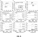
- the graphs show:
- the temperature of etching process was constant at 600 °C for (b, d-i).
- the total film thickness of the as-grown 3-5 ML MoS 2 film on sapphire is around 3.6 ML as calculated from Rutherford backscattering spectrometry (RBS) measurements.
- the Cl 2 etching speed of the as-grown 3.6 ML MoS 2 is evaluated at various etching temperatures, including 500 °C and 600 °C in FIG. 3a .
- the etching speed increases with the etching temperature.
- the etching speed which is initially quite high (0.5-1 ML/minute depending on the temperature), decreases after some time of etching to ⁇ 0.1 ML/minute (the slope in FIG. 3a gets less steep with the etching time), indicating etching of the closed layers is much more difficult than the superficial islands. This allows a selective etching of the superficial islands without damaging the underneath closed layer(s).
- the etching selection ratio can be optimized through different etchants, temperature, pressure, gas flow, time and others.
- FIG. 3b further illustrates the selective etching through the A 1g and E 2g peak frequency difference of the 3-5 ML MoS 2 before and after different etching time at 600 °C.
- the A 1g and E 2g peak frequency difference of MoS 2 decreases with the film thickness, as it can be observed for as grown 3-5 ML and 1-2 ML MoS 2 . Similar to that in FIG. 3a , A 1g and E 2g peak frequency difference decreases with the etching time and the decreasing slope becomes gentle with the etching time.
- This Cl 2 thermal etching process is gentle, which doesn't change the pristine properties of the as grown MoS 2 on sapphire.
- the measured S/Mo ratio stays around 2 for the MoS 2 after different etching times at both 500 °C and 600 °C, as illustrated in FIG. 3c .
- the XPS spectra of CI 2p show negligible peaks for the MoS 2 before and after 1 min, 8 min and 9 min etching in FIG. 3f , indicating no CI bonds with the MoS 2 after etching.
- the characteristic peaks all exist in Raman and PL spectra for the MoS2 after different etching time in FIG. 3h-i .
- the slightly shift of the peak position in FIG. 3i is due to the thickness reduction with the etching time.
- the etching process doesn't change the pristine physical properties of the as-grown MoS 2 .
- FIG. 4 When providing a film using the exemplary method, in accordance with embodiments of the present invention, it is illustrated in FIG. 4 that surface smoothness of the epitaxial MoS 2 on sapphire after Cl 2 etching can be achieved. This is illustrated for 3-5 ML and 1-2 ML MoS 2 on sapphire after Cl 2 etching.
- FIG. 4 (a-d) show the topography obtained using AFM (atomic force microscopy) of as-grown 3-5 ML MoS 2 ( FIG. 4a ) and the topography obtained after different etching times ( FIG. 4b-d ).
- AFM atomic force microscopy
- FIG. 4 (e-f) show the topography obtained using AFM of as-grown 1-2 ML MoS 2 before ( FIG. 4e ) and after 0.5 min of etching ( FIG. 4f ).
- FIG. 4 (g-h) shows the zoom in topography maps of (e-f).
- the surface coverage of superficial crystals in (e, g) is around 5%, while it reduces to ⁇ 1% in (f, h).
- FIG. 4i shows the full width at half maximum (FWHM) of the E 2g peak of the as-grown 1-2 ML MoS 2 and the one after 0.5 min etching.
- FIG. 4j shows the full width at half maximum (FWHM) of the A 1g peak of the as-grown 1-2 ML MoS 2 and the one after 0.5 min etching.
- the as-grown 3-5 ML MoS 2 comprises a closed film of 3 MLs of MoS 2 with 4th ML, 5th ML crystals and vertical growth on top ( FIG. 4a ).
- the surface roughness of this as-grown 3-5 ML MoS 2 is around 5.76 nm.
- the Cl 2 etching process the vertical growth, the 5 th and 4 th ML crystals disappear ( FIG. 4b-d ).
- the surface roughness also decreases ( FIG. 4b-d ).
- Embodiments of the present invention provide a method for manufacturing a field effect transistor.
- the method comprises providing 100 a film of one or more monolayers of transition metal dichalcogenides on a substrate, using a method according to any of the previous claims.
- the method moreover, comprises forming a gate stack on top of the film of the transition metal dichalcogenides such that the film is a channel of the field effect transistor, and forming source and drain contacts at the beginning and end of the channel.
- FIG. 8 shows a schematic drawing of an exemplary FET stack obtained using a method in accordance with embodiments of the present invention.
- the stack 400 comprises a Si substrate 410, a SiO 2 layer 420, a first metal layer 430, a high-k dielectric 440, an MX 2 channel 450, source and drain contacts 460a of a second metal, 460b, and metal contacts (of a third metal) 470a and 470b with the source and drain contacts.
- This is only an exemplary FET stack, and also other FET stacks known by the person skilled in the art are possible.
- Essential is that the channel is a MX 2 channel obtained using a method in accordance with embodiments of the present invention.
- the electrical properties of epitaxial MoS 2 after etching further confirm that the Cl 2 thermal etching process doesn't damage the closed MoS 2 layers under the superficial islands, and there is no doping effect induced by the Cl 2 etching.
- the typical transfer characteristic curves of pristine (reference numbers 1 and 2) and etched 3-5 layer MoS 2 (reference numbers 3 and 4) based field-effect transistors (FETs) in FIG. 5 reveal that there is no shift of the threshold voltage (Vt) for the Cl 2 etched MoS 2 based transistors at all the channel lengths (L ch ), compared to that of pristine MoS 2 based transistors. This indicates there is no doping effect introduced by this Cl 2 thermal etching process.
- the minimum drain current (I min ) of the pristine MoS 2 based transistors is larger than that of etched MoS 2 based transistors at all the L ch .
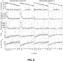
- FIG. 6 shows the statistical comparison of the electrical properties of pristine and etched MoS 2 based transistors. From top to bottom the following graphs are shown:
- the transistors are fabricated on 3-5 ML MoS 2 before (samples with reference numbers 1 and 2; the two left columns) and after 9 min Cl2 etching (samples with reference numbers 3 and 4; the two right columns.
- the maximum drain current (Imax) of the etched MoS 2 based transistors does not decrease in FIG. 6a , compared to that of the pristine MoS 2 based transistors. This confirms that the Cl 2 thermal etching process is gentle, which doesn't damage the closed MoS 2 layers under the superficial crystals.
- FIG. 6b shows that the I min of the pristine MoS 2 based transistors is larger than that of the etched MoS 2 based transistors, especially for transistors with shorter L ch .
- SSmin minimum subthreshold swing
- the threshold voltage Vt of the pristine and the etched MoS 2 based transistors is substantially the same, thus this further confirms the Cl 2 thermal etching doesn't introduce any doping to the MoS 2 layers.
- the calculated field effect mobility ( ⁇ FE) of the pristine and etched MoS 2 based transistors is similar, and this further confirms the Cl 2 thermal etching doesn't damage the MoS 2 layers under the superficial crystals. Thus, this in-situ Cl 2 thermal etching process is gentle and can etch the superficial crystals on top of the closed 2D layers selectively.
- FIG. 7 shows an example of MOCVD WS 2 crystals grown on a SiO 2 /Si surface.
- the dashed circles outline the small crystals grown on SiO 2 /Si and the first ML WS 2 crystals.
- a process is introduced including cycles of deposition and selective etching to remove the small crystals (the superficial islands) and then regrow the layer until the 1 st ML closes.
- SE etch the etching selection ratio
- [W] 2 nd ML represents the amount of material to be removed
- [ W ] 1 st ML represents the amount of material to be kept.
- a method according to embodiments of the present invention may be used for selective area deposition.
- the provided 110 substrate is a patterned substrate comprising a first material and a second material
- the at least one monolayer of the transition metal dichalcogenides is deposited 120 on the patterned substrate and the materials are selected such that the deposition is more inhibited on the second material than on the first material.
- the high temperature etching 130 is such that nuclei of the transition metal dichalcogenides on the second material are removed from the second material.
- the transition metal dichalcogenide, the first material and the second material are selected such that the deposition of the transition metal dichalcogenide is more inhibited on the second material than on the first material.
- the first material of the patterned substrate can for example be HfO 2 and the second material SiO 2 .
- the deposition step one monolayer of MX 2 is selectively deposited on HfO 2 as the materials are selected such that the MX 2 deposition is more inhibited on SiO 2 .
- a certain selectively loss can be expected w.r.t. SiO 2 resulting in the formation of MX 2 nuclei in the first monolayer also on SiO 2 . It is an advantage of embodiments of the present invention that these are selectively removed from the SiO 2 surface using thermal etch process.
- the first material can be MoS 2 and the second material SiO 2 .
- the MX 2 material may be different from the first material. It may for example be WS 2 , or HfS 2 .
- the MX 2 material is selectively deposited on the first material MoS 2 to form a heterostructure.
- the thermal etch process is used to selectively etch MX 2 layer that nucleates on the second material SiO 2 to have the MX 2 layer only forming on the first material.
- the method may comprise transferring the provided film from the substrate on which it is formed to a target substrate.
- the transfer may be achieved via wet or dry transfer methods. In the wet transfer case, it may be based on water assisted delamination.
- a layer of PMMA may for example be firstly coated on the MX 2 film grown on sapphire.
- a thermal release tape TRT
- the MX 2 film may be delaminated from the sapphire through water intercalation in ambient.
- the target substrate e.g. SiO 2
- the TRT can be released at ⁇ 150 °C.
- the PMMA may be removed through acetone and Isopropyl alcohol, which results in the clean MX 2 film on the target substrates.
Landscapes
- Drying Of Semiconductors (AREA)
Abstract
Description
- The invention relates to the field of metal chalcogenide films. More specifically it relates to a method for forming providing a film of one or more monolayers of transition metal dichalcogenides on a substrate.
- Two-dimensional transition metal dichalcogenide (MX2) films attract lots of attention for next-generation electronics, optoelectronics and photonics. They could play an important role in beyond-CMOS (complementary metal-oxide-semiconductor) electronics.
- The semiconducting group-VI MX2 materials possess a layered crystal structure with layer-dependent physical and electrical properties, and a chemically inert surface free of dangling bonds. As such, MX2 materials complement Silicon as channel material in nanoelectronic devices with ultra-scaled channel thickness at excellent electrostatic gate control and anticipated absence of interface defects, and decreased off-state power consumption. However, their unique properties predominantly excel in one monolayer film and few monolayer film form, which fuels research on the large-area deposition of atomically thin MX2 material.
- The structural and electrical quality of two-dimensional transition metal dichalcogenide films (2D MX2 films) are highly dependent on the absence of defects and the smoothness of the film surface. The point defect, grin boundaries and surface roughness of 2D materials make it more challenging for the integration and industrialization of 2D materials based nanoelectronics.
- Towards the large-area integration of 2D materials based nanoelectronics, one of the biggest challenges is to achieve uniform and wafer-scale single (or highly) crystalline deposition of the 2D MX2 materials. The misorientation of the first monolayer crystals can result in grain boundaries, which is one kind of local defects that can degrade the advanced electronic properties of 2D materials.
- There is therefore a need to achieve uniform and wafer-scale single (or highly) crystalline deposition of the 2D MX2 materials.
- It is an object of embodiments of the present invention to provide a good method for providing a film of one or more monolayers of transition metal dichalcogenides on a substrate.
- In embodiments of the present invention this is achieved by a method in which first a substrate is provided and in which, furthermore, a sequence is provided which comprises the following steps:
- depositing at least one monolayer of the transition metal dichalcogenides on the substrate,
- selectively removing superficial islands on top of the at least one monolayer by thermal etching.
- In embodiments of the present invention wherein the sequence of depositing/selectively removing is executed at least twice. The sequence may be executed until one or more closed monolayers are obtained.
- In embodiments of the present invention etchants used for the etching may be selected from the list of CI2, HCI, CO.
- In embodiments of the present invention the transition metal dichalcogenides are deposited by metal-organic chemical vapor deposition.
- A method, according to embodiments of the present invention, may be applied on any substrate, as long as the main growth mode of the MX2 layer is planar, since it is based on the presence of dangling bonds on island edges, vs. a fully saturated basal plane surface. The substrate can for example be a sapphire substrate.
- In embodiments of the present invention the transition metal dichalcogenide is MoS2. The invention is, however, not limited thereto. Also other transition metal dichalcogenides may be used, such as for example WS2.
- In embodiments of the present invention the depositing and selective removing are done in a same reactor. It is an advantage of embodiments of the present invention that reactivation, which would be required when moving the substrate from one reactor to another, can be avoided by growing and etching in the same reactor.
- In embodiments of the present invention the selective removing is done at a temperature of at least 500°C.
- In embodiments of the present invention the method is suitable for selective area deposition, wherein:
- the provided substrate is a patterned substrate comprising a first material and a second material,
- the at least one monolayer of the transition metal dichalcogenides is deposited on the patterned substrate and the materials are selected such that the deposition is more inhibited on the second material than on the first material,
- the high temperature etching is such that nuclei of the transition metal dichalcogenides on the second material are removed from the second material.
- In embodiments of the present invention the transition metal is a metal from group VI of the periodic table of elements.
- In embodiments of the present invention a method is provided for manufacturing a field effect transistor. The method comprises providing a film of one or more monolayers of transition metal dichalcogenides on a substrate, using a method according to embodiments of the present invention.
- The method, moreover, comprises forming a gate stack on top of the film of the transition metal dichalcogenides such that the film is a channel of the field effect transistor, and forming source and drain contacts at the beginning and end of the channel.
- It is an advantage of embodiments of the present invention that MX2 materials are replacing Si as channel material. It is an advantage of embodiments of the present invention that the channel thickness can be reduced to a few or even one monolayer and that superficial islands are removed.
- In embodiments of the present invention the method comprises transferring the provided film from the substrate on which it is formed to a target substrate.
- In summary, it is an advantage of embodiments of the present invention that by means of the (in-situ) selective etching process an increased flexibility to tune the deposition process of epitaxial 2D MX2 materials can be achieved. This enables to control the local film thickness and thus surface smoothness and to achieve uniform, wafer-scale and single (highly) crystalline 1 ML film of 2D MX2 materials. A method according to embodiments of the present invention may for example be used for controlling the local film thickness variation of wafer-scale epitaxial 2D MX2 materials and thus smoothening the surface. It may for example also be used for wafer-scale single (highly) crystalline growth of 2D MX2 materials for advanced high-performance nanoelectronics and optoelectronics. Another application may be the anisotropic etching (with hard mask) techniques of 2D materials for nanoelectronics fabrication and integration.
- Particular and preferred aspects of the invention are set out in the accompanying independent and dependent claims. Features from the dependent claims may be combined with features of the independent claims and with features of other dependent claims as appropriate and not merely as explicitly set out in the claims.
- These and other aspects of the invention will be apparent from and elucidated with reference to the embodiment(s) described hereinafter.
-
-
FIG. 1 shows a flow chart of a method an exemplary method in accordance with embodiments of the present invention. -
FIG. 2 schematically illustrate one cycle of growth and selective etching on wafer-scale epitaxial 2D materials, in accordance with embodiments of the present invention. -
FIG. 3 illustrates physical properties of a MoS2 film obtained using a method in accordance with embodiments of the present invention. -
FIG. 4 illustrates the surface smoothness of an epitaxial MoS2 film before and after etching, it is illustrated that surface smoothness can be achieved using a method in accordance with embodiments of the present invention. -
FIG. 5 shows the transfer curves of pristine and etched 3-5 layer MoS2 based field effect transistors, the latter being obtained using a method in accordance with embodiments of the present invention. -
FIG. 6 shows the electrical performance of pristine MoS2 based FETs and of etched MoS2 based FETs, the latter being obtained using a method in accordance with embodiments of the present invention. -
FIG. 7 shows an image of MOCVD WS2 crystals grown on a SiO2/Si surface and a graph illustrating the effect of the etching selection ratio on the film obtained using a method in accordance with embodiments of the present invention. -
FIG. 8 shows a schematic drawing of a FET stack wherein the channel is an MX2 channel which is obtained using a method in accordance with embodiments of the present invention. - Any reference signs in the claims shall not be construed as limiting the scope. In the different drawings, the same reference signs refer to the same or analogous elements.
- The present invention will be described with respect to particular embodiments and with reference to certain drawings but the invention is not limited thereto but only by the claims. The drawings described are only schematic and are non-limiting. In the drawings, the size of some of the elements may be exaggerated and not drawn on scale for illustrative purposes. The dimensions and the relative dimensions do not correspond to actual reductions to practice of the invention.
- The terms first, second and the like in the description and in the claims, are used for distinguishing between similar elements and not necessarily for describing a sequence, either temporally, spatially, in ranking or in any other manner. It is to be understood that the terms so used are interchangeable under appropriate circumstances and that the embodiments of the invention described herein are capable of operation in other sequences than described or illustrated herein.
- It is to be noticed that the term "comprising", used in the claims, should not be interpreted as being restricted to the means listed thereafter; it does not exclude other elements or steps. It is thus to be interpreted as specifying the presence of the stated features, integers, steps or components as referred to, but does not preclude the presence or addition of one or more other features, integers, steps or components, or groups thereof. Thus, the scope of the expression "a device comprising means A and B" should not be limited to devices consisting only of components A and B. It means that with respect to the present invention, the only relevant components of the device are A and B.
- Reference throughout this specification to "one embodiment" or "an embodiment" means that a particular feature, structure or characteristic described in connection with the embodiment is included in at least one embodiment of the present invention. Thus, appearances of the phrases "in one embodiment" or "in an embodiment" in various places throughout this specification are not necessarily all referring to the same embodiment, but may. Furthermore, the particular features, structures or characteristics may be combined in any suitable manner, as would be apparent to one of ordinary skill in the art from this disclosure, in one or more embodiments.
- Similarly it should be appreciated that in the description of exemplary embodiments of the invention, various features of the invention are sometimes grouped together in a single embodiment, figure, or description thereof for the purpose of streamlining the disclosure and aiding in the understanding of one or more of the various inventive aspects. This method of disclosure, however, is not to be interpreted as reflecting an intention that the claimed invention requires more features than are expressly recited in each claim. Rather, as the following claims reflect, inventive aspects lie in less than all features of a single foregoing disclosed embodiment. Thus, the claims following the detailed description are hereby expressly incorporated into this detailed description, with each claim standing on its own as a separate embodiment of this invention.
- Furthermore, while some embodiments described herein include some but not other features included in other embodiments, combinations of features of different embodiments are meant to be within the scope of the invention, and form different embodiments, as would be understood by those in the art. For example, in the following claims, any of the claimed embodiments can be used in any combination.
- In the description provided herein, numerous specific details are set forth. However, it is understood that embodiments of the invention may be practiced without these specific details. In other instances, well-known methods, structures and techniques have not been shown in detail in order not to obscure an understanding of this description.
- Where in embodiments of the present invention reference is made to a monolayer ML, reference is made to a layer of transition metal dichalcogenides (MX2, with M a transition metal, and X a chalcogen).
- Where in embodiments of the present invention reference is made to an MX2 film, reference is made to a film on a substrate, composed of one or more monolayers of MX2.
- In embodiments of the present invention the thickness of a monolayer depends on the transition metal M and on the chalcogenide X. This thickness is typically around 0.6 nm.
- Where in embodiments of the present invention reference is made to the number of monolayers (NOML), reference is made to the number of monolayers stacked on top of each other.
- The total film thickness is the physical thickness of the provided MX2 film. It depends on the NOML and on the transition metal M and on the chalcogenide X. For example a MX2 film containing exactly 2 MLs of MX2 is designated as a "2 ML film" and a MX2 film of exactly 1 ML is designated as a "1 ML film or single ML film".
- Embodiments of the present invention relate to a
method 100 for providing a film of one or more monolayers of transition metal dichalcogenides on a substrate. The method comprises: - providing 110 a substrate;
- depositing 120 at least one monolayer of the transition metal dichalcogenides on the substrate,
- selectively removing 130 superficial islands on top of the at least one monolayer by thermal etching.
- A flow chart of an exemplary method in accordance with embodiments of the present invention is show in
FIG. 1 . - It is an advantage of embodiments of the present invention that the superficial islands are removed. Without being bound by theory, it is assumed that this is possible because of a different etch rate between the superficial islands on the monolayer, and the monolayer itself. It is assumed that the reason therefore is that the etchants first react at the edges of the MX2 islands or MX2 flakes due to existence of dangling bonds, rather than the planar surface which is free of dangling bonds. In embodiments of the present invention the etching reaction is, therefore, not conformal, but rather selective to superficial islands.
- In embodiments of the present invention a basal plane of the film is parallel with a surface of the wafer.
- In embodiments of the present invention a monolayer of transition metal dichalcogenides is a one-molecular 2D layer of transition metal dichalcogenides (MX2, with M a transition metal, and X a chalcogen), with its basal plane parallel aligned to the wafer surface, and containing only one central layer of M-atoms, cladded above and below by a layer of X atoms.
- In embodiments of the present invention selective removal of the superficial islands on top of the at least one monolayer is done by thermal etching, whereby etchants such as CI2, HCI or CO are used.
- In embodiments of the present invention a setup is used that allows the growth and etching process of 2D MX2 in the same reactor. With such a setup it is possible to etch away the undesirable superficial MX2 islands in-situ and selectively after the growth, and thus the surface of MX2 gets smoothened.
- It is an advantage of embodiments of the present invention that the selective etching process is gentle and doesn't modify the physical properties of 2D materials, which actually improves the electrical performance of MX2 based transistors in terms of minimum current (i.e. the off-current, Imin) and subthreshold swing (SSmin).
- In embodiments of the present invention the depositing/selectively removing
sequence - It is, thereby, an advantage that the number of monolayers, and the variation thereon, can be controlled by executing cycles of growth and etching. Thus, a smoothened surface can be obtained. It is an advantage of embodiments of the present invention that it is possible to selectively etch the superficial islands without damaging the underneath closed layers. When reference is made to a closed layer, reference is made to a layer without an opening in the layer. A closed layer, on the other hand, is a fully coalesced layer without any holes/openings.
- By combining cycles of the selective etching process with cycles of deposition, the deposition of uniform and wafer-scale single (highly) crystalline one monolayer MX2 film can be achieved. A method according to embodiments of the present invention enables precise control of 2D film thickness and thus surface smoothness. Moreover, it also provides new methods for the nanofabrication and integration process of 2D materials based nanoelectronics and optoelectronics.
- The total film thickness can be controlled through tuning parameters of the growth process, such as the growth time. Moreover, a selective and gentle etching process, according to embodiments of the present invention, after growth, helps to etch away the superficial islands without damaging the lower-lying closed 2D layer(s).
- The drawings in
FIG. 2 schematically illustrate one cycle of growth and selective etching on wafer-scale epitaxial 2D materials. The top drawings inFIG. 2 show a schematic drawing of a stack of monolayers 221-222, 231-233, including superficial islands, on adeposition substrate 210. As illustrated in the top drawings ofFIG. 2 , unwanted superficial islands 231-233 are existing on top of the lower-lying,closed 2D 1ML film 221 ofmulti-ML film crystal 241 is grown at a discontinuity in thesecond monolayer 222. The superficial islands are grown anisotropically on top of the lower lying layer(s) before the underlying layer(s) is closed. Therefore, in embodiments of the present invention, a thermal etching process is applied directly after the growth. - This etching process should be gentle and can remove the superficial islands selectively. The selectivity of the etching process can be engineered by a judicious choice of the species of the etchants, and careful tuning of process parameters such as temperature, pressure, gas flow, time, etc. In embodiments of the present invention etchants used for the
etching 130 may for example be selected from the list of Cl2, HCl, CO. This list is not limiting and also other etchants may be selected. In embodiments of the present invention the selective removing 130 is preferably done at temperatures of at least 500°C. The temperatures are preferably between 500°C and 600°C. It is an advantage of embodiments of the present invention that the cycle of growth and etching can help to reduce the local NOML variation of the deposited 2D layers and thus smoothen the surface. InFIG. 2 the schematic drawings at the bottom show the obtained stack after selective etching. - Without being bound by theory, it is assumed that the reaction kinetics of the etchants (such as CI2, HCI, CO, etc.) with 2D superficial islands is different from the reaction kinetics of fully closed layers of 2D materials. The etchants firstly attack the edges of 2D islands due to the existence of dangling bonds, rather than the planar surface which is free of dangling bonds.
- In embodiments of the present invention defects during the etching process may be avoided by the addition of H2S (or other sulphur-containing precursors) during the etching process.
- In an exemplary embodiment of the present invention firstly, epitaxial molybdenum disulfide (MoS2) is deposited 120 on
sapphire wafers 210 through metal-organic chemical vapor deposition (MOCVD) in an industry-compatible reactor. Thesapphire wafers 210 are firstly placed on a 200 mm silicon pocket wafer (structure: 100 nm ALD Al2O3/2000 nm SiO2/Si) which contains 4 pockets with size of 2-inch and then loaded to the MOCVD reactor. The MOCVD equipment for the experiment consists of a single wafer (≥ 200 mm) and lamp-heated reactor with gas flow controlled by mass flow controllers, which allows large-scale deposition of MX2 on wafers with size as large as 200 mm. After loading the sapphire wafers to the reactor, the wafers are heated to 1000 °C under high-purity N2 in the reactor, then 100 standard cubic centimeter per minute (sccm) H2S (carried by 20 standard liter per minute (slm) N2) and 80 sccm Ar:Mo(CO)6 gas precursor (Ar is the carrier gas for the metal precursor) are sent to the reactor. High purity H2S, N2 and Ar gas are provided through compressed gas cylinders. The MO(CO)6 is vaporized from the solid precursor in a metallic canister (from Air liquide) at about 26 °C under about 900 mbar. During the growth, the growth temperature is kept at 1000 °C and the total pressure is constant at 20 Torr. For the growth of 1-2 ML (1 ML film with 2nd ML islands) and 3-5 ML (3 ML film with 4th and 5th ML islands) films of MoS2 on sapphire, the growth time is 6 min and 20 min respectively at this condition. - After the growth, the etching process follows immediately in the same reactor. The etching process is performed under the condition of 20 sccm Cl2 and 20 slm N2 at a total pressure of 20 Torr. The temperature for the etching process is constant. Two kinds of temperature conditions are tried, including 600 °C and 500 °C. After the etching process, all the samples are annealed in the same chamber under 100 sccm H2S (carried by 20 slm N2) at 1000 °C and at a total pressure of 90 Torr.
- The selective etching of epitaxial MoS2 grown on sapphire through in-situ Cl2 thermal etching is demonstrated in
FIG. 3 . - The graphs show:
- (a) thickness of 3-5 ML MoS2 before etching and after different etching times at different temperatures;
- (c) S/Mo ratio of 3-5 ML MoS2 before etching and after different etching times at different temperatures;
- (b) A1g and E2g peak frequency difference of 3-5 ML MoS2 before and after etching, and as-grown 1-2 ML MoS2;
- (d) X-ray photoelectron spectroscopy (XPS) of
Mo 3d before etching and after different etching times; - (e) XPS of
S 2p before etching and after different etching times; - (f) XPS of
CI 2p before etching and after different etching times; - (g) XPS of
O 1s before etching and after different etching times; - (h) Raman spectroscopy of 3-5 ML MoS2 before etching and after different etching times;
- (i) Photoluminescence (PL) spectrum of 3-5 ML MoS2 before etching and after different etching times.
- The temperature of etching process was constant at 600 °C for (b, d-i).
- The total film thickness of the as-grown 3-5 ML MoS2 film on sapphire is around 3.6 ML as calculated from Rutherford backscattering spectrometry (RBS) measurements. The Cl2 etching speed of the as-grown 3.6 ML MoS2 is evaluated at various etching temperatures, including 500 °C and 600 °C in
FIG. 3a . The etching speed increases with the etching temperature. Most importantly, the etching speed which is initially quite high (0.5-1 ML/minute depending on the temperature), decreases after some time of etching to ~0.1 ML/minute (the slope inFIG. 3a gets less steep with the etching time), indicating etching of the closed layers is much more difficult than the superficial islands. This allows a selective etching of the superficial islands without damaging the underneath closed layer(s). The etching selection ratio can be optimized through different etchants, temperature, pressure, gas flow, time and others. -
FIG. 3b further illustrates the selective etching through the A1g and E2g peak frequency difference of the 3-5 ML MoS2 before and after different etching time at 600 °C. The A1g and E2g peak frequency difference of MoS2 decreases with the film thickness, as it can be observed for as grown 3-5 ML and 1-2 ML MoS2. Similar to that inFIG. 3a , A1g and E2g peak frequency difference decreases with the etching time and the decreasing slope becomes gentle with the etching time. - This Cl2 thermal etching process is gentle, which doesn't change the pristine properties of the as grown MoS2 on sapphire. The measured S/Mo ratio stays around 2 for the MoS2 after different etching times at both 500 °C and 600 °C, as illustrated in
FIG. 3c . - Furthermore, the XPS spectra of the
Mo 3d,S 2p andO 1s all stay the same before and after 1 min, 8 min and 9 min etching inFIG. 3-e, g . - Meanwhile, the XPS spectra of
CI 2p show negligible peaks for the MoS2 before and after 1 min, 8 min and 9 min etching inFIG. 3f , indicating no CI bonds with the MoS2 after etching. - The characteristic peaks all exist in Raman and PL spectra for the MoS2 after different etching time in
FIG. 3h-i . The slightly shift of the peak position inFIG. 3i is due to the thickness reduction with the etching time. According to all of these physical characterizations of the epitaxial MoS2 grown on sapphire before and after different etching time, the etching process doesn't change the pristine physical properties of the as-grown MoS2. - When providing a film using the exemplary method, in accordance with embodiments of the present invention, it is illustrated in
FIG. 4 that surface smoothness of the epitaxial MoS2 on sapphire after Cl2 etching can be achieved. This is illustrated for 3-5 ML and 1-2 ML MoS2 on sapphire after Cl2 etching. -
FIG. 4 (a-d) show the topography obtained using AFM (atomic force microscopy) of as-grown 3-5 ML MoS2 (FIG. 4a ) and the topography obtained after different etching times (FIG. 4b-d ). -
FIG. 4 (e-f) show the topography obtained using AFM of as-grown 1-2 ML MoS2 before (FIG. 4e ) and after 0.5 min of etching (FIG. 4f ). -
FIG. 4 (g-h) shows the zoom in topography maps of (e-f). The surface coverage of superficial crystals in (e, g) is around 5%, while it reduces to <1% in (f, h). -
FIG. 4i shows the full width at half maximum (FWHM) of the E2g peak of the as-grown 1-2 ML MoS2 and the one after 0.5 min etching. -
FIG. 4j shows the full width at half maximum (FWHM) of the A1g peak of the as-grown 1-2 ML MoS2 and the one after 0.5 min etching. - Both peaks are narrowing after etching. The temperature of etching process is constant at 600 °C.
- As mentioned above, the as-grown 3-5 ML MoS2 comprises a closed film of 3 MLs of MoS2 with 4th ML, 5th ML crystals and vertical growth on top (
FIG. 4a ). The surface roughness of this as-grown 3-5 ML MoS2 is around 5.76 nm. With the Cl2 etching process, the vertical growth, the 5th and 4th ML crystals disappear (FIG. 4b-d ). Moreover, the surface roughness also decreases (FIG. 4b-d ). These observations are further confirmed for the etching of as-grown 1-2 ML MoS2 film (FIG. 4e-h ). There is a clear reduction for surface coverage of superficial crystals on top of the closed monolayer MoS2 before and after 0.5 min etching process (from ~5% inFIG. 4e, g to <1% inFigure 4f, h ). Meanwhile, the size of the superficial crystals also decreases after etching (FIG. 4g-h ). As a result, the whole surface roughness decreases. Moreover, the E2g and A1g peaks of the 1-2 ML MoS2 become narrower after etching, indicating the sample surface after etching is more uniform. - Embodiments of the present invention provide a method for manufacturing a field effect transistor. The method comprises providing 100 a film of one or more monolayers of transition metal dichalcogenides on a substrate, using a method according to any of the previous claims. The method, moreover, comprises forming a gate stack on top of the film of the transition metal dichalcogenides such that the film is a channel of the field effect transistor, and forming source and drain contacts at the beginning and end of the channel.
-
FIG. 8 shows a schematic drawing of an exemplary FET stack obtained using a method in accordance with embodiments of the present invention. Thestack 400 comprises aSi substrate 410, a SiO2 layer 420, afirst metal layer 430, a high-k dielectric 440, an MX2 channel 450, source anddrain contacts 460a of a second metal, 460b, and metal contacts (of a third metal) 470a and 470b with the source and drain contacts. This is only an exemplary FET stack, and also other FET stacks known by the person skilled in the art are possible. Essential is that the channel is a MX2 channel obtained using a method in accordance with embodiments of the present invention. - In the following paragraphs physical properties of pristine and etched 3-5 layer MoS2 based field effect transistors are evaluated.
- The electrical properties of epitaxial MoS2 after etching further confirm that the Cl2 thermal etching process doesn't damage the closed MoS2 layers under the superficial islands, and there is no doping effect induced by the Cl2 etching. The typical transfer characteristic curves of pristine (
reference numbers 1 and 2) and etched 3-5 layer MoS2 (reference numbers 3 and 4) based field-effect transistors (FETs) inFIG. 5 reveal that there is no shift of the threshold voltage (Vt) for the Cl2 etched MoS2 based transistors at all the channel lengths (Lch), compared to that of pristine MoS2 based transistors. This indicates there is no doping effect introduced by this Cl2 thermal etching process. Moreover, the minimum drain current (Imin) of the pristine MoS2 based transistors is larger than that of etched MoS2 based transistors at all the Lch. - This is further confirmed in
FIG. 6 through comparing the electrical performance of 1080 transistors fabricated with the pristine and etched MoS2 layers.FIG. 6 shows the statistical comparison of the electrical properties of pristine and etched MoS2 based transistors. From top to bottom the following graphs are shown: - (a) Imax;
- (b) Imin;
- (c) SSmin;
- (d) Vt;
- (e) µFE.
- The transistors are fabricated on 3-5 ML MoS2 before (samples with
reference numbers reference numbers - The maximum drain current (Imax) of the etched MoS2 based transistors does not decrease in
FIG. 6a , compared to that of the pristine MoS2 based transistors. This confirms that the Cl2 thermal etching process is gentle, which doesn't damage the closed MoS2 layers under the superficial crystals. - Similar to
FIG. 5 ,FIG. 6b shows that the Imin of the pristine MoS2 based transistors is larger than that of the etched MoS2 based transistors, especially for transistors with shorter Lch. - A similar phenomenon is also observed for minimum subthreshold swing (SSmin). As can be seen in
FIG. 6c , the SSmin of the pristine MoS2 based transistors is larger than that of the etched MoS2 based transistors, especially for transistors with shorter Lch. - From the graphs in
FIG. 6d it can be seen that the threshold voltage Vt of the pristine and the etched MoS2 based transistors is substantially the same, thus this further confirms the Cl2 thermal etching doesn't introduce any doping to the MoS2 layers. The calculated field effect mobility (µFE) of the pristine and etched MoS2 based transistors is similar, and this further confirms the Cl2 thermal etching doesn't damage the MoS2 layers under the superficial crystals. Thus, this in-situ Cl2 thermal etching process is gentle and can etch the superficial crystals on top of the closed 2D layers selectively. - As discussed earlier, it is an advantage of embodiments of the present invention that a uniform and wafer-scale single (or highly) crystalline epitaxial deposition of single monolayer 2D materials can be obtained. Before the closure of the 1st ML of 2D materials, the coexistence of big and small 1st ML crystals, and also 2nd ML crystals on top of the 1st ML crystals can be observed. This is illustrated in
FIG. 7 . The left image inFIG. 7 shows an example of MOCVD WS2 crystals grown on a SiO2/Si surface. The dashed circles outline the small crystals grown on SiO2/Si and the first ML WS2 crystals. These small 1st ML and 2nd ML crystals can introduce more grain boundaries and local defects, which should be avoided during the deposition process. Therefore, in embodiments of the present invention, a process is introduced including cycles of deposition and selective etching to remove the small crystals (the superficial islands) and then regrow the layer until the 1st ML closes. Through tuning the etching parameters, the etching selection ratio (SEetch) can be tuned. The etching selection ratio can be expressed as:
- In this equation [W]2 ndML represents the amount of material to be removed, while [W]1 stML represents the amount of material to be kept. When SEetch is close to zero, there are big and small MX2 crystals existing simultaneously, as shown in the inset schematic 310 in the right graph of
FIG. 7 . When SEetch increases, the small crystals are expected to be removed through etching and just the large crystals are left, as shown in the inset schematic 320 in the right graph ofFIG. 7 . It is an advantage of embodiments of the present invention that with increasing number of cycles of the deposition and selective etching process, the uniformity of the film increases. Thus, a uniform and wafer-scale single (or highly) crystalline 1 ML film can be obtained. Hence, it is, moreover, an advantage that using a method in accordance with embodiments of the present invention also a multi-ML film of 2D materials with a controlled NOML can be obtained. - A method according to embodiments of the present invention may be used for selective area deposition. In such a method, the provided 110 substrate is a patterned substrate comprising a first material and a second material, and the at least one monolayer of the transition metal dichalcogenides is deposited 120 on the patterned substrate and the materials are selected such that the deposition is more inhibited on the second material than on the first material. Moreover, the
high temperature etching 130 is such that nuclei of the transition metal dichalcogenides on the second material are removed from the second material. - In embodiments of the present invention the transition metal dichalcogenide, the first material and the second material are selected such that the deposition of the transition metal dichalcogenide is more inhibited on the second material than on the first material.
- In an exemplary embodiment of the present invention the first material of the patterned substrate can for example be HfO2 and the second material SiO2. In the deposition step one monolayer of MX2 is selectively deposited on HfO2 as the materials are selected such that the MX2 deposition is more inhibited on SiO2. However, a certain selectively loss can be expected w.r.t. SiO2 resulting in the formation of MX2 nuclei in the first monolayer also on SiO2. It is an advantage of embodiments of the present invention that these are selectively removed from the SiO2 surface using thermal etch process.
- In an exemplary embodiment of the present invention the first material can be MoS2 and the second material SiO2. The MX2 material may be different from the first material. It may for example be WS2, or HfS2. The MX2 material is selectively deposited on the first material MoS2 to form a heterostructure. The thermal etch process is used to selectively etch MX2 layer that nucleates on the second material SiO2 to have the MX2 layer only forming on the first material. As such, one can deposit heterostructure of MoS2 with another MX2 layer (e.g., WS2, HfS2).
- In embodiments of the present invention the method may comprise transferring the provided film from the substrate on which it is formed to a target substrate.
- The transfer may be achieved via wet or dry transfer methods. In the wet transfer case, it may be based on water assisted delamination. A layer of PMMA may for example be firstly coated on the MX2 film grown on sapphire. Then a thermal release tape (TRT) may be used for the transfer of the MX2 from sapphire to other substrates. The MX2 film may be delaminated from the sapphire through water intercalation in ambient. After transferring the TRT/PMMA/MX2 on the target substrate (e.g. SiO2), the TRT can be released at ~150 °C. Finally, the PMMA may be removed through acetone and Isopropyl alcohol, which results in the clean MX2 film on the target substrates.
Claims (12)
- A method (100) for providing a film of one or more monolayers of transition metal dichalcogenides on a substrate, the method comprising:- providing (110) a substrate,the method, furthermore, comprising a sequence of:- depositing (120) at least one monolayer of the transition metal dichalcogenides on the substrate,- selectively removing (130) superficial islands on top of the at least one monolayer by thermal etching.
- A method (100) according to claim 1 wherein the depositing/selectively removing sequence (120, 130) of claim 1 is executed at least twice.
- A method (100) according to any of the previous claims wherein etchants used for the etching (130) are selected from the list of Cl2, HCl, CO.
- A method (100) according to any of the previous claims wherein the transition metal dichalcogenides are deposited (120) by metal-organic chemical vapor deposition.
- A method (100) according to any of the previous claims wherein the substrate is a sapphire substrate.
- A method (100) according to any of the previous claims wherein the transition metal dichalcogenide is MoS2.
- A method (100) according to any of the previous claims wherein the depositing (120) and selective removing (130) are done in a same reactor.
- A method (100) according to any of the previous claims wherein the selective removing (130) is done at a temperature of at least 500°C.
- A method (100) according to any of the previous claims wherein the method (100) is suitable for selective area deposition, wherein:- the provided (110) substrate is a patterned substrate comprising a first material and a second material,- the at least one monolayer of the transition metal dichalcogenides is deposited (120) on the patterned substrate and the materials are selected such that the deposition is more inhibited on the second material than on the first material,- the high temperature etching (130) is such that nuclei of the transition metal dichalcogenides on the second material are removed from the second material.
- A method (100) according to any of the previous claims wherein the transition metal is a metal from group VI of the periodic table of elements.
- A method for manufacturing a field effect transistor, the method comprising providing (100) a film of one or more monolayers of transition metal dichalcogenides on a substrate, using a method according to any of the previous claims,- forming a gate stack on top of the film of the transition metal dichalcogenides such that the film is a channel of the field effect transistor,- forming source and drain contacts at the beginning and end of the channel.
- A method according to claim 11, the method comprising transferring the provided film from the substrate on which it is formed (100) to a target substrate.
Priority Applications (3)
| Application Number | Priority Date | Filing Date | Title |
|---|---|---|---|
| EP21159840.4A EP4053879A1 (en) | 2021-03-01 | 2021-03-01 | Deposition of highly crystalline 2d materials |
| US17/677,005 US12112946B2 (en) | 2021-03-01 | 2022-02-22 | Deposition of highly crystalline 2D materials |
| CN202210197354.4A CN114999894A (en) | 2021-03-01 | 2022-03-01 | Deposition of highly crystalline 2D materials |
Applications Claiming Priority (1)
| Application Number | Priority Date | Filing Date | Title |
|---|---|---|---|
| EP21159840.4A EP4053879A1 (en) | 2021-03-01 | 2021-03-01 | Deposition of highly crystalline 2d materials |
Publications (1)
| Publication Number | Publication Date |
|---|---|
| EP4053879A1 true EP4053879A1 (en) | 2022-09-07 |
Family
ID=74844766
Family Applications (1)
| Application Number | Title | Priority Date | Filing Date |
|---|---|---|---|
| EP21159840.4A Pending EP4053879A1 (en) | 2021-03-01 | 2021-03-01 | Deposition of highly crystalline 2d materials |
Country Status (3)
| Country | Link |
|---|---|
| US (1) | US12112946B2 (en) |
| EP (1) | EP4053879A1 (en) |
| CN (1) | CN114999894A (en) |
Citations (2)
| Publication number | Priority date | Publication date | Assignee | Title |
|---|---|---|---|---|
| US20180163312A1 (en) * | 2016-12-09 | 2018-06-14 | Asm Ip Holding B.V. | Thermal atomic layer etching processes |
| DE102019114131A1 (en) * | 2018-09-25 | 2020-03-26 | Taiwan Semiconductor Manufacturing Co., Ltd. | FIELD EFFECT TRANSISTOR USING TRANSITION METAL DICHALCOGENIDE AND METHOD FOR THE PRODUCTION THEREOF |
Family Cites Families (7)
| Publication number | Priority date | Publication date | Assignee | Title |
|---|---|---|---|---|
| US8207023B2 (en) | 2009-08-06 | 2012-06-26 | Applied Materials, Inc. | Methods of selectively depositing an epitaxial layer |
| US8642454B2 (en) | 2011-05-19 | 2014-02-04 | International Business Machines Corporation | Low temperature selective epitaxy of silicon germanium alloys employing cyclic deposit and etch |
| US9093468B2 (en) | 2013-03-13 | 2015-07-28 | Taiwan Semiconductor Manufacturing Company, Ltd. | Asymmetric cyclic depositon and etch process for epitaxial formation mechanisms of source and drain regions |
| US10283319B2 (en) | 2016-12-22 | 2019-05-07 | Asm Ip Holding B.V. | Atomic layer etching processes |
| US10319588B2 (en) | 2017-10-10 | 2019-06-11 | Asm Ip Holding B.V. | Method for depositing a metal chalcogenide on a substrate by cyclical deposition |
| US10731249B2 (en) | 2018-02-15 | 2020-08-04 | Asm Ip Holding B.V. | Method of forming a transition metal containing film on a substrate by a cyclical deposition process, a method for supplying a transition metal halide compound to a reaction chamber, and related vapor deposition apparatus |
| US11393681B2 (en) | 2018-03-07 | 2022-07-19 | Uchicago Argonne, Llc | Methods to deposit and etch controlled thin layers of transition metal dichalcogenides |
-
2021
- 2021-03-01 EP EP21159840.4A patent/EP4053879A1/en active Pending
-
2022
- 2022-02-22 US US17/677,005 patent/US12112946B2/en active Active
- 2022-03-01 CN CN202210197354.4A patent/CN114999894A/en active Pending
Patent Citations (2)
| Publication number | Priority date | Publication date | Assignee | Title |
|---|---|---|---|---|
| US20180163312A1 (en) * | 2016-12-09 | 2018-06-14 | Asm Ip Holding B.V. | Thermal atomic layer etching processes |
| DE102019114131A1 (en) * | 2018-09-25 | 2020-03-26 | Taiwan Semiconductor Manufacturing Co., Ltd. | FIELD EFFECT TRANSISTOR USING TRANSITION METAL DICHALCOGENIDE AND METHOD FOR THE PRODUCTION THEREOF |
Non-Patent Citations (5)
| Title |
|---|
| BRENT JACK R ET AL: "Synthetic approaches to two-dimensional transition metal dichalcogenide nanosheets", PROGRESS IN MATERIALS SCIENCE, PERGAMON PRESS, GB, vol. 89, 10 June 2017 (2017-06-10), pages 411 - 478, XP085137132, ISSN: 0079-6425, DOI: 10.1016/J.PMATSCI.2017.06.002 * |
| DANIELE CHIAPPE ET AL: "Layer-controlled epitaxy of 2D semiconductors: bridging nanoscale phenomena to wafer-scale uniformity", NANOTECHNOLOGY, IOP PUBLISHING, ENGLAND, vol. 29, no. 42, 17 August 2018 (2018-08-17), pages 425602, XP020331275, ISSN: 0957-4484, [retrieved on 20180817], DOI: 10.1088/1361-6528/AAD798 * |
| LIN TAIZHE ET AL: "Controlled Layer-by-Layer Etching of MoS 2", APPLIED MATERIALS & INTERFACES, vol. 7, no. 29, 29 July 2015 (2015-07-29), US, pages 15892 - 15897, XP055825254, ISSN: 1944-8244, DOI: 10.1021/acsami.5b03491 * |
| LU XIN ET AL: "Layer-by-layer thinning of MoS 2 by thermal annealing", NANOSCALE, vol. 5, no. 19, January 2013 (2013-01-01), United Kingdom, pages 8904 - 8908, XP055825246, ISSN: 2040-3364, DOI: 10.1039/C3NR03101B * |
| WU JUMIATI ET AL: "Layer Thinning and Etching of Mechanically Exfoliated MoS 2 Nanosheets by Thermal Annealing in Air", SMALL, 28 August 2013 (2013-08-28), pages n/a - n/a, XP055825570, ISSN: 1613-6810, DOI: 10.1002/smll.201301542 * |
Also Published As
| Publication number | Publication date |
|---|---|
| US20220277953A1 (en) | 2022-09-01 |
| US12112946B2 (en) | 2024-10-08 |
| CN114999894A (en) | 2022-09-02 |
Similar Documents
| Publication | Publication Date | Title |
|---|---|---|
| EP0828287A2 (en) | Improvements in or relating to semiconductors | |
| US20200357635A1 (en) | Large-scale synthesis of 2d semiconductors by epitaxial phase conversion | |
| CN103633115B (en) | Apparatus and method for multiple gate transistors | |
| EP3255656B1 (en) | A method for forming a vertical hetero-stack and a device including a vertical hetero-stack | |
| TWI785993B (en) | Apparatus and method for manipulating artificial two-dimensional materials at the atomic level | |
| Ramdani et al. | Interface characterization of high-quality SrTiO3 thin films on Si (100) substrates grown by molecular beam epitaxy | |
| US12112946B2 (en) | Deposition of highly crystalline 2D materials | |
| Cho et al. | Selectable synthesis of 2-D MoS 2 and its electronic devices: From isolated triangular islands to large-area continuous thin film | |
| JP2764049B2 (en) | Method of manufacturing compound semiconductor device, compound semiconductor device and field effect transistor | |
| US20200381540A1 (en) | Semiconductor device, manufacturing method thereof, and electronic device including the device | |
| Pandey et al. | Growth of very large MoS 2 single crystals using out-diffusion transport and their use in Field effect transistors | |
| Lee et al. | Improved long-term stability of low-temperature polysilicon thin-film transistors by using a tandem gate insulator with an atomic layer of deposited silicon dioxide | |
| EP3648146B1 (en) | Removing an organic sacrificial material from a 2d material | |
| Chou et al. | Improved monolayer mos performance with two-step atomic layer deposited high-dielectrics | |
| CN222967310U (en) | Semiconductor components | |
| US6548335B1 (en) | Selective epitaxy to reduce gate/gate dielectric interface roughness | |
| Destefanis et al. | Fabrication, structural and electrical properties of (1 1 0) localized silicon-on-insulator devices | |
| WO2025221641A1 (en) | Direct heterogeneous integration of oxide materials on transition metal dichalcogenides | |
| US12400925B1 (en) | Field effect transistor including transition metal dichalcogenide covered with protective layer, and method of manufacturing the same | |
| JP4138719B2 (en) | Method for manufacturing insulated gate field effect transistor | |
| WO2025125554A1 (en) | 2d channel field-effect transistor device | |
| US20250183036A1 (en) | Selective silicon nitride with treatment for contact formation in logic or memory devices | |
| JP3614333B2 (en) | Insulated gate type field effect transistor fabrication method | |
| CN1747130A (en) | Production of Si-base quantum point structure based on metal induced crystallizing process | |
| Bauer et al. | Low temperature selective epitaxial growth of SiCP on Si (110) oriented surfaces |
Legal Events
| Date | Code | Title | Description |
|---|---|---|---|
| PUAI | Public reference made under article 153(3) epc to a published international application that has entered the european phase |
Free format text: ORIGINAL CODE: 0009012 |
|
| STAA | Information on the status of an ep patent application or granted ep patent |
Free format text: STATUS: THE APPLICATION HAS BEEN PUBLISHED |
|
| AK | Designated contracting states |
Kind code of ref document: A1 Designated state(s): AL AT BE BG CH CY CZ DE DK EE ES FI FR GB GR HR HU IE IS IT LI LT LU LV MC MK MT NL NO PL PT RO RS SE SI SK SM TR |
|
| STAA | Information on the status of an ep patent application or granted ep patent |
Free format text: STATUS: REQUEST FOR EXAMINATION WAS MADE |
|
| 17P | Request for examination filed |
Effective date: 20230306 |
|
| RBV | Designated contracting states (corrected) |
Designated state(s): AL AT BE BG CH CY CZ DE DK EE ES FI FR GB GR HR HU IE IS IT LI LT LU LV MC MK MT NL NO PL PT RO RS SE SI SK SM TR |
|
| STAA | Information on the status of an ep patent application or granted ep patent |
Free format text: STATUS: EXAMINATION IS IN PROGRESS |
|
| 17Q | First examination report despatched |
Effective date: 20250904 |