EP4053876A1 - Radiation tube and radiation source - Google Patents
Radiation tube and radiation source Download PDFInfo
- Publication number
- EP4053876A1 EP4053876A1 EP22158547.4A EP22158547A EP4053876A1 EP 4053876 A1 EP4053876 A1 EP 4053876A1 EP 22158547 A EP22158547 A EP 22158547A EP 4053876 A1 EP4053876 A1 EP 4053876A1
- Authority
- EP
- European Patent Office
- Prior art keywords
- unit
- anode
- cathode
- radiation
- constant voltage
- Prior art date
- Legal status (The legal status is an assumption and is not a legal conclusion. Google has not performed a legal analysis and makes no representation as to the accuracy of the status listed.)
- Pending
Links
Images



Classifications
-
- H—ELECTRICITY
- H01—ELECTRIC ELEMENTS
- H01J—ELECTRIC DISCHARGE TUBES OR DISCHARGE LAMPS
- H01J35/00—X-ray tubes
- H01J35/02—Details
- H01J35/025—X-ray tubes with structurally associated circuit elements
-
- H—ELECTRICITY
- H05—ELECTRIC TECHNIQUES NOT OTHERWISE PROVIDED FOR
- H05G—X-RAY TECHNIQUE
- H05G1/00—X-ray apparatus involving X-ray tubes; Circuits therefor
- H05G1/08—Electrical details
- H05G1/085—Circuit arrangements particularly adapted for X-ray tubes having a control grid
-
- H—ELECTRICITY
- H05—ELECTRIC TECHNIQUES NOT OTHERWISE PROVIDED FOR
- H05G—X-RAY TECHNIQUE
- H05G1/00—X-ray apparatus involving X-ray tubes; Circuits therefor
- H05G1/08—Electrical details
- H05G1/10—Power supply arrangements for feeding the X-ray tube
- H05G1/12—Power supply arrangements for feeding the X-ray tube with DC or rectified single-phase AC or double-phase
-
- H—ELECTRICITY
- H05—ELECTRIC TECHNIQUES NOT OTHERWISE PROVIDED FOR
- H05G—X-RAY TECHNIQUE
- H05G1/00—X-ray apparatus involving X-ray tubes; Circuits therefor
- H05G1/08—Electrical details
- H05G1/26—Measuring, controlling or protecting
- H05G1/30—Controlling
- H05G1/32—Supply voltage of the X-ray apparatus or tube
-
- H—ELECTRICITY
- H05—ELECTRIC TECHNIQUES NOT OTHERWISE PROVIDED FOR
- H05G—X-RAY TECHNIQUE
- H05G1/00—X-ray apparatus involving X-ray tubes; Circuits therefor
- H05G1/08—Electrical details
- H05G1/26—Measuring, controlling or protecting
- H05G1/30—Controlling
- H05G1/34—Anode current, heater current or heater voltage of X-ray tube
-
- H—ELECTRICITY
- H01—ELECTRIC ELEMENTS
- H01J—ELECTRIC DISCHARGE TUBES OR DISCHARGE LAMPS
- H01J35/00—X-ray tubes
- H01J35/02—Details
- H01J35/04—Electrodes ; Mutual position thereof; Constructional adaptations therefor
- H01J35/06—Cathodes
- H01J35/065—Field emission, photo emission or secondary emission cathodes
-
- H—ELECTRICITY
- H01—ELECTRIC ELEMENTS
- H01J—ELECTRIC DISCHARGE TUBES OR DISCHARGE LAMPS
- H01J35/00—X-ray tubes
- H01J35/02—Details
- H01J35/04—Electrodes ; Mutual position thereof; Constructional adaptations therefor
- H01J35/08—Anodes; Anti cathodes
-
- H—ELECTRICITY
- H01—ELECTRIC ELEMENTS
- H01J—ELECTRIC DISCHARGE TUBES OR DISCHARGE LAMPS
- H01J35/00—X-ray tubes
- H01J35/02—Details
- H01J35/16—Vessels; Containers; Shields associated therewith
Definitions
- the present disclosure relates to a radiation tube and a radiation source.
- a radiation source which emits radiation to an object in a case in which a radiographic image of the object is captured.
- the radiation source includes a radiation tube that generates radiation.
- As the radiation tube in addition to a radiation tube that heats a filament as an electrode to emit thermal electrons, a radiation tube comprising a cold cathode that emits electrons without heating the electrode is known.
- the radiation tube comprises: an electron emitting unit that includes a cathode unit and a gate electrode for applying a voltage to the cathode unit and constitutes a cold cathode; an anode unit that has an anode surface facing the cathode unit; and a constant voltage supply unit that supplies a constant driving voltage to the gate electrode (see, for example, JP2012-33411A ).
- the electron emitting unit and the anode unit are accommodated in a vacuum tube, and the constant voltage supply unit is provided outside the vacuum tube.
- the radiation source comprises a housing that accommodates the radiation tube.
- the constant voltage supply unit is provided outside the vacuum tube of the radiation tube and inside the housing, since an outer wall of the housing has a ground potential, a sufficient distance is required between the constant voltage supply unit and the outer wall of the housing.
- the present disclosure has been made in view of the above circumstances, and an object of the present disclosure is to provide a radiation tube and a radiation source that have a smaller size than those in the related art.
- a radiation tube that is used in a radiation source for radiography.
- the radiation tube comprises: an electron emitting unit that includes a cathode unit having an emitter electrode which emits electrons and a gate electrode; an anode unit that has an anode surface facing the cathode unit and collides with the electrons to generate radiation; a constant voltage supply unit that supplies a constant driving voltage to the gate electrode; and a vacuum tube that accommodates the electron emitting unit, the anode unit, and the constant voltage supply unit.
- the constant voltage supply unit may include a Zener diode that is connected in parallel to the gate electrode and the cathode unit and a smoothing capacitor that is connected in parallel to the Zener diode.
- the constant voltage supply unit may further include a temperature compensation diode that is connected in series to the Zener diode.
- At least the Zener diode of the constant voltage supply unit may be mounted on the same substrate as the electron emitting unit.
- a constant voltage substrate on which the constant voltage supply unit is formed may be disposed to come into contact with an electron emitting unit substrate on which the electron emitting unit is formed.
- a constant voltage substrate on which the constant voltage supply unit is formed may be disposed to be separated from an electron emitting unit substrate on which the electron emitting unit is formed.
- a radiation source comprising: the radiation tube according to the present disclosure; an anode-side booster circuit unit that is provided outside a vacuum tube of the radiation tube and supplies a boosted anode voltage to the anode unit; and a cathode-side booster circuit unit that is provided outside the vacuum tube and supplies a boosted cathode voltage to the cathode unit.
- a driving voltage boosted by the cathode-side booster circuit unit may be higher than a power supply voltage boosted by the anode-side booster circuit unit.
- the anode-side booster circuit unit may include an anode transformer
- the cathode-side booster circuit unit may include a cathode transformer that has a higher ratio of the number of turns of a secondary coil to the number of turns of a primary coil than the anode transformer.
- the anode-side booster circuit unit may include an anode capacitor that accumulates charge corresponding to the boosted power supply voltage
- the cathode-side booster circuit unit may include a cathode capacitor that accumulates charge corresponding to the boosted driving voltage and has a higher capacitance than the anode capacitor
- the radiation source according to any one of the seventh to tenth aspects may further comprise a housing that accommodates the radiation tube.
- the radiation source comprising the radiation tube can have a smaller size than that in the related art.
- Fig. 1 is a side view illustrating an example of the outward appearance of a mammography apparatus 10 according to this embodiment.
- Fig. 1 illustrates an example of the outward appearance of the mammography apparatus 10 as viewed from the left side of a subject.
- the mammography apparatus 10 is an apparatus that is operated under the control of a console (not illustrated) and irradiates a breast of the subject as an object with radiation R (for example, X-rays) to capture a radiographic image of the breast.
- the mammography apparatus 10 may be an apparatus that images the breast of the subject not only in a state in which the subject is standing (standing state) but also in a state in which the subject is sitting on, for example, a chair (including a wheelchair) (sitting state).
- the mammography apparatus 10 comprises a control unit 40, a storage unit 42, and an interface (I/F) unit 44 which are provided in an imaging table 24.
- the control unit 40 controls the overall operation of the mammography apparatus 10 under the control of the console.
- the control unit 40 comprises a central processing unit (CPU), a read only memory (ROM), and a random access memory (RAM) which are not illustrated.
- CPU central processing unit
- ROM read only memory
- RAM random access memory
- various programs including an imaging processing program which is executed by the CPU and is used to perform control related to the capture of radiographic images are stored in the ROM in advance.
- the RAM temporarily stores various kinds of data.
- image data of a radiographic image captured by a radiation detector 20 and various other kinds of information are stored in the storage unit 42.
- a specific example of the storage unit 42 is a hard disk drive (HDD), a solid state drive (SSD), or the like.
- the I/F unit 44 transmits and receives various kinds of information to and from the console using wireless communication or wired communication.
- the image data of the radiographic image captured by the radiation detector 20 in the mammography apparatus 10 is transmitted to an external device, such as the console, through the I/F unit 44 by wireless communication or wired communication.
- the operation unit 46 is, for example, a plurality of switches that are provided in the imaging table 24 of the mammography apparatus 10 or the like. Further, the operation unit 46 may be provided as a touch panel switch or may be provided as a foot switch that is operated by the feet of the user such as a doctor or a radiology technician.
- the radiation detector 20 is disposed in the imaging table 24.
- the breast of the subject is positioned on an imaging surface 24A of the imaging table 24 by a user.
- the radiation detector 20 detects the radiation R transmitted through the breast which is the object. Specifically, the radiation detector 20 detects the radiation R that has entered the breast of the subject and an imaging table 24 and reached the detection surface 20A of the radiation detector 20, generates a radiographic image on the basis of the detected radiation R, and outputs image data indicating the generated radiographic image.
- the type of the radiation detector 20 according to this embodiment is not particularly limited.
- the radiation detector 20 may be an indirect-conversion-type radiation detector that converts the radiation R into light and converts the converted light into charge or a direct-conversion-type radiation detector that directly converts the radiation R into charge.
- a compression plate 38 that is used to compress the breast in a case in which imaging is performed is attached to a compression unit 36 that is provided in the imaging table 24.
- the compression unit 36 is provided with a compression plate driving unit (not illustrated) that moves the compression plate 38 in a direction (hereinafter, referred to as an "up-down direction") toward or away from the imaging table 24.
- a support portion 39 of the compression plate 38 is detachably attached to the compression plate driving unit and is moved in the up-down direction by the compression plate driving unit to compress the breast of the subject between the compression plate 38 and the imaging table 24.
- the mammography apparatus 10 comprises the imaging table 24, the arm portion 33, a base 34, and a shaft portion 35.
- the arm portion 33 is held by the base 34 so as to be movable in the up-down direction (Z-axis direction).
- the arm portion 33 can be rotated with respect to the base 34 by the shaft portion 35.
- the shaft portion 35 is fixed to the base 34, and the shaft portion 35 and the arm portion 33 are rotated integrally.
- Gears are provided in each of the shaft portion 35 and the compression unit 36 of the imaging table 24.
- the gears can be switched between an engaged state and a non-engaged state to switch between a state in which the compression unit 36 of the imaging table 24 and the shaft portion 35 are connected and rotated integrally and a state in which the shaft portion 35 is separated from the imaging table 24 and runs idle.
- components for switching between the transmission and non-transmission of the power of the shaft portion 35 are not limited to the gears, and various mechanical elements may be used.
- Each of the arm portion 33 and the imaging table 24 can be relatively rotated with respect to the base 34, using the shaft portion 35 as a rotation axis.
- engagement portions (not illustrated) are provided in each of the base 34, the arm portion 33, and the compression unit 36 of the imaging table 24. The state of the engagement portions is switched to connect each of the arm portion 33 and the compression unit 36 of the imaging table 24 to the base 34.
- One or both of the arm portion 33 and the imaging table 24 connected to the shaft portion 35 are integrally rotated on the shaft portion 35.
- the mammography apparatus 10 can perform simple imaging that captures an image of an object in a posture in which a radiation source 29 faces the radiation detector 20 and can also perform so-called tomosynthesis imaging that captures images a plurality of times while relatively moving the radiation source 29 with respect to the radiation detector 20 to change the irradiation angle of the radiation R with respect to the object.
- the tomosynthesis imaging is performed in the mammography apparatus 10
- the radiation source 29 is moved to each of a plurality of irradiation positions having different irradiation angles by the rotation of the arm portion 33.
- the radiation source 29 generates the radiation R under the control of the control unit 40 and emits the generated radiation R to the object.
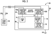
- Fig. 2 is a block diagram illustrating an example of the configuration of the radiation source 29 according to this embodiment. As illustrated in Fig. 2 , the radiation source 29 comprises a radiation tube 60, a booster circuit unit 62, and a housing 64. The housing 64 is connected to the ground potential GND and accommodates the radiation tube 60 and the booster circuit unit 62.
- a predetermined voltage is supplied to the booster circuit unit 62 from a power supply device 25 that is provided in the base 34 through a voltage cable 25A.
- the booster circuit unit 62 has a function of boosting the predetermined voltage supplied from the power supply device 25 through the voltage cable 25A and supplying the boosted voltage to the radiation tube 60.
- the booster circuit unit 62 includes an anode-side booster circuit unit 63A and a cathode-side booster circuit unit 63B.
- the anode-side booster circuit unit 63A is provided outside a vacuum tube 76 of the radiation tube 60 and supplies a boosted anode voltage to an anode unit 74 of the radiation tube 60.
- the anode-side booster circuit unit 63A boosts the voltage supplied from the power supply device 25 through the voltage cable 25A and supplies the boosted voltage as the anode voltage to the anode unit 74 of the radiation tube 60.
- the cathode-side booster circuit unit 63B is provided outside the vacuum tube 76 of the radiation tube 60 and supplies a boosted cathode voltage to an electron emitting unit 72 of the radiation tube 60. Specifically, the cathode-side booster circuit unit 63B boosts the voltage supplied from the power supply device 25 through the voltage cable 25A and supplies the boosted voltage as the cathode voltage to the electron emitting unit 72 of the radiation tube 60.
- the radiation tube 60 is used in the radiation source 29 for radiography and generates the radiation R according to the anode voltage and the cathode voltage supplied from the booster circuit unit 62.
- the radiation tube 60 comprises a constant voltage supply unit 70, the electron emitting unit 72, the anode unit 74, and the vacuum tube 76.
- the electron emitting unit 72 has a function of emitting electrons according to the cathode voltage supplied from the cathode-side booster circuit unit 63B.
- the constant voltage supply unit 70 has a function of supplying a constant driving voltage to a gate electrode 96 (see Fig. 3 , which will be described in detail below) of the electron emitting unit 72.
- the anode unit 74 has a function of generating the radiation R using the electrons emitted by the electron emitting unit 72.
- the vacuum tube 76 has a function of accommodating the constant voltage supply unit 70, the electron emitting unit 72, and the anode unit 74.
- the vacuum tube 76 has, for example, a cylindrical shape and is made of glass, ceramic, or the like.
- the inside of the vacuum tube 76 is hermetically sealed and is kept in a vacuum state.
- Fig. 3 is a diagram illustrating an example of a circuit configuration of the radiation tube 60 and the booster circuit unit 62 according to this embodiment.
- the electron emitting unit 72 has a cathode unit 90 and the gate electrode 96.
- the cathode unit 90 includes an emitter electrode 92 that has an electron emitting element 94 formed on a support substrate 91 made of, for example, silicon.
- the emitter electrode 92 according to this embodiment is composed of a field emitter array in which a plurality of electron emitting elements 94 that emit electrons in a case in which an electric field is applied from the outside are arranged in a matrix.
- the electron emitting element 94 has, for example, a conical shape with a sharp tip.
- an electron emitting element of the spinto-type emitter electrode 92 that is formed by the vapor deposition of molybdenum on the support substrate 91 is used.
- the gate electrode 96 is an electrode for applying the electric field to the cathode unit 90.
- the gate electrode 96 is provided on the emitter electrode 92 through an insulation layer 95.
- the gate electrode 96 has a plurality of opening portions which are formed so as to surround each electron emitting element 94 and are arranged in a matrix so as to correspond to each electron emitting element 94. Electrons are emitted from the opening portions.
- a method for forming the gate electrode 96 and the cathode unit 90 is as follows. First, an oxide film which is a material forming the gate electrode 96 is formed on the support substrate 91, and a resist is formed on the oxide film according to a pattern of the gate electrode 96. After the resist is formed, the oxide film is etched to form an opening portion in the oxide film. A portion of the oxide film in which no resist is formed becomes the opening portion. After the opening portion is formed, a molybdenum film which is a material forming the electron emitting element 94 is formed by vapor deposition. Therefore, the emitter electrode 92 having the conical electron emitting element 94 formed in the opening portion is formed. In Fig.
- the cathode unit 90 and the gate electrode 96 are drawn so as to be separated from each other.
- the cathode unit 90 and the gate electrode 96 are formed on one support substrate 91.
- a carbon nanotube may be used as the material forming the electron emitting element 94.
- the cathode unit 90 and the gate electrode 96 are formed as one chip.
- the constant voltage supply unit 70 includes a Zener diode 80, a temperature compensation diode 82, and a smoothing capacitor 84.
- the Zener diode 80 is connected in parallel to the gate electrode 96 and the cathode unit 90. Specifically, in the Zener diode 80, a cathode is connected to the gate electrode 96, and an anode is connected to a wiring line for applying the cathode voltage to the cathode unit 90 through the temperature compensation diode 82.
- the Zener diode 80 has a function of making the voltage supplied to the gate electrode 96 constant even in a case in which a current flowing from the gate electrode 96 changes.
- the temperature compensation diode 82 is connected in series to the Zener diode 80.
- the Zener diode 80 generates heat in a case in which a current flows from the gate electrode 96. Therefore, the temperature compensation diode 82 is a diode that is provided in a forward direction in order to cancel a temperature coefficient of the Zener diode 80.
- Fig. 3 illustrates an aspect in which one temperature compensation diode 82 is connected in series to the Zener diode 80.
- the number of temperature compensation diodes 82 provided is not limited to this aspect, and any number of temperature compensation diodes 82 may be provided according to the temperature coefficient of the Zener diode 80 as long as they can cancel the temperature coefficient.
- the smoothing capacitor 84 is connected in parallel to the Zener diode 80.
- the smoothing capacitor 84 has a function of suppressing voltage ripple between the gate electrode 96 and the cathode unit 90. Specifically, in a case in which the voltage is high, charge is accumulated in the smoothing capacitor 84. In a case in which the voltage is low, the accumulated charge is discharged to suppress the fluctuation of the voltage between the gate electrode 96 and the cathode unit 90.
- the anode unit 74 has an anode surface 75 that faces the cathode unit 90.
- the electrons emitted from the electron emitting unit 72 collide with the anode surface 75, and the anode unit 74 generates the radiation R.
- the anode unit 74 is made of, for example, copper.
- the anode-side booster circuit unit 63A of the booster circuit unit 62 includes an anode transformer 50A which is a boosting transformer, diodes 54A and 55A, and capacitors 52A and 53A.
- the capacitor 52A and the capacitor 53A are connected in series between the anode unit 74 and the cathode-side booster circuit unit 63B.
- one end of the capacitor 52A is connected to the anode unit 74, and the other end of the capacitor 52A is connected to one end of the capacitor 53A.
- the other end of the capacitor 53A is connected to the cathode-side booster circuit unit 63B.
- the capacitor 52A and the capacitor 53A according to this embodiment are an example of an anode transistor according to the present disclosure.
- the diode 54A and the diode 55A are connected in series to each other and are connected in parallel to the capacitor 52A and the capacitor 53A. Specifically, a cathode of the diode 54A is connected to the one end of the capacitor 52A, and an anode of the diode 54A is connected to a cathode of the diode 55A. An anode of the diode 55A is connected to the other end of the capacitor 53A.
- the anode transformer 50A is a boosting transformer and includes a primary coil 51A 1 that is connected to the power supply device 25 and a secondary coil 51A 2 for supplying a voltage to the anode unit 74.
- the anode transformer 50A boosts the voltage supplied from the power supply device 25 to an anode voltage corresponding to the ratio of the number of turns of the secondary coil 51A 2 to the number of turns of the primary coil 51A 1 .
- One end of the secondary coil 51A 2 is connected to a midpoint of the diode 54A and the diode 55A.
- the other end of the secondary coil 51A 2 is connected to a midpoint of the capacitor 52A and the capacitor 53A.
- the anode-side booster circuit unit 63A boosts the voltage supplied from the power supply device 25 using the anode transformer 50A, rectifies and accumulates the voltage using the diodes 54A and 55A and the capacitors 52A and 53A, and supplies the anode voltage to the anode unit 74.
- the cathode-side booster circuit unit 63B of the booster circuit unit 62 has the same configuration as the anode-side booster circuit unit 63A.
- the cathode-side booster circuit unit 63B has a cathode transformer 50B which is a boosting transformer, diodes 54B and 55B, and capacitors 52B and 53B.
- the capacitor 52B and the capacitor 53B are connected in series between the anode-side booster circuit unit 63A and the cathode unit 90.
- one end of the capacitor 52B is connected to the anode-side booster circuit unit 63A, and the other end of the capacitor 52B is connected to one end of the capacitor 53B.
- the other end of the capacitor 53B is connected to the cathode unit 90.
- the capacitor 52B and the capacitor 53B according to this embodiment are an example of a cathode transistor according to the present disclosure.
- the diode 54B and the diode 55B are connected in series to each other and are connected in parallel to the capacitor 52B and the capacitor 53B. Specifically, a cathode of the diode 54B is connected to the one end of the capacitor 52B, and an anode of the diode 54B is connected to a cathode of the diode 55B. An anode of the diode 55B is connected to the other end of the capacitor 53B.
- the cathode transformer 50B is a boosting transformer and includes a primary coil 51Bi that is connected to the power supply device 25 and a secondary coil 51B 2 for supplying a voltage to the cathode unit 90.
- the cathode transformer 50B boosts the voltage supplied from the power supply device 25 to a cathode voltage corresponding to the ratio of the number of turns of the secondary coil 51B 2 to the number of turns of the primary coil 51Bi.
- One end of the secondary coil 51B 2 is connected to a midpoint of the diode 54B and the diode 55B.
- the other end of the secondary coil 51B 2 is connected to a midpoint of the capacitor 52B and the capacitor 53B.
- the other end of the secondary coil 51B2 is connected to a midpoint of the capacitor 52B and the capacitor 53B has been described for ease of understanding.
- the other end of the secondary coil 51B2 does not necessarily have to be connected to the midpoint of the capacitor 52B and the capacitor 53B, and may be connected to parts with different potential differences (whichever may be larger).
- the cathode-side booster circuit unit 63B boosts the voltage supplied from the power supply device 25 using the cathode transformer 50B, rectifies and accumulates the voltage using the diodes 54B and 55B and the capacitors 52B and 53B, and supplies the cathode voltage to the cathode unit 90.
- the ratio of the number of turns of the secondary coil 51B 2 to the number of turns of the primary coil 51Bi in the cathode transformer 50B is higher than the ratio of the number of turns of the secondary coil 51A 2 to the number of turns of the primary coil 51A 1 in the anode transformer 50A.
- the turn ratio of the cathode transformer 50B is higher than the turn ratio of the anode transformer 50A. That is, the degree of boosting of the cathode transformer 50B is larger than that of the anode transformer 50A.
- the capacitances of the capacitors 52B and 53B of the cathode-side booster circuit unit 63B are higher than the capacitances of the capacitors 52A and 53A of the anode-side booster circuit unit 63A. Therefore, the capacitors 52B and 53B of the cathode-side booster circuit unit 63B can accumulate a larger amount of charge than the capacitors 52A and 53A of the anode-side booster circuit unit 63A.
- the cathode unit 90 emits electrons as described above, it is preferable that the cathode voltage supplied to the cathode unit 90 is larger than the anode voltage.
- the turn ratio of the cathode transformer 50B is higher than that of the anode transformer 50A, it is possible to generate a cathode voltage that is larger than the anode voltage.
- the capacitances of the capacitors 52B and 53B of the cathode-side booster circuit unit 63B are higher than those of the capacitors 52A and 53A of the anode-side booster circuit unit 63A, it is possible to stably supply a cathode voltage that is larger than the anode voltage to the cathode unit 90.
- the cathode voltage is supplied to the cathode unit 90 and the anode voltage is applied to the anode unit 74, a tube current corresponding to the Zener voltage of the Zener diode 80 is generated, and the radiation R corresponding to the tube current is generated.
- the cathode voltage has a negative potential
- the anode voltage has a positive potential.
- the constant voltage supply unit 70 supplies a constant voltage as the driving voltage for driving the gate electrode 96. Therefore, it is possible to stabilize the gate voltage supplied to the gate electrode 96. It is possible to stabilize the amount of radiation R generated by the radiation tube 60.
- Fig. 4 is a cross-sectional view illustrating the constant voltage supply unit 70 and the electron emitting unit 72 according to this configuration example.
- the constant voltage supply unit 70 and the electron emitting unit 72 according to this configuration example are mounted on the same substrate and are formed as a so-called one chip.
- the Zener diode 80 and the temperature compensation diode 82 of the constant voltage supply unit 70 are mounted on the support substrate 91 of the cathode unit 90.
- the Zener diode 80 and the temperature compensation diode 82 can be formed as surface-mounted components on the support substrate 91 similarly to the cathode unit 90. Therefore, as in the aspect illustrated in Fig.
- the electron emitting unit 72, the Zener diode 80, and the temperature compensation diode 82 may be integrated into one chip.
- the smoothing capacitor 84 of the constant voltage supply unit 70 and the electron emitting unit 72 may not be integrated into one chip. That is, it is not necessary to mount the smoothing capacitor 84 on the support substrate 91.
- the smoothing capacitor 84 can be disposed at any position.
- the smoothing capacitor 84 may be formed on a substrate different from the support substrate 91, which will be described in the following Configuration Examples 2 and 3.
- the constant voltage supply unit 70 and the electron emitting unit 72 are mounted on the same substrate.
- the constant voltage supply unit 70 and the electron emitting unit 72 are integrated into one chip. Therefore, according to the radiation tube 60 of this configuration example, it is possible to reduce the size of the radiation tube 60. Further, it is possible to manufacture the constant voltage supply unit 70 and the electron emitting unit 72 at the same time and thus to improve the manufacturing yield.
- Fig. 5 is a cross-sectional view illustrating the constant voltage supply unit 70 and the electron emitting unit 72 according to this configuration example.
- the constant voltage supply unit 70 and the electron emitting unit 72 according to this configuration example are formed on separate substrates.
- a substrate on which the constant voltage supply unit 70 is formed and a substrate on which the electron emitting unit 72 is formed are provided so as to be separated from each other.
- the support substrate 91 on which the cathode unit 90 of the electron emitting unit 72 is formed and a constant voltage substrate 85 on which the constant voltage supply unit 70 is formed are provided so as to be separated from each other.
- the constant voltage substrate 85 is provided so as to face a surface opposite to the surface on which the electron emitting element 94 is formed in the support substrate 91 of the cathode unit 90.
- a stem pin 98 for supplying the cathode voltage to the cathode unit 90 passes through the constant voltage substrate 85.
- An insulating material 86 is provided in a portion of the constant voltage substrate 85 through which the stem pin 98 passes.
- the electron emitting element 94 and the constant voltage substrate 85 are connected by a gate line 97, and a driving voltage is supplied from the constant voltage supply unit 70 to the constant voltage substrate 85 through the gate line 97.
- the constant voltage supply unit 70 and the electron emitting unit 72 are formed on separate substrates, and the substrate on which the constant voltage supply unit 70 is formed and the substrate on which the electron emitting unit 72 is formed are provided so as to be separated from each other.
- the constant voltage supply unit 70 and the electron emitting unit 72 are integrated into one chip as in Configuration Example 1 and a defect occurs in either the constant voltage supply unit 70 or the electron emitting unit 72, the entire chip is defective.
- the constant voltage supply unit 70 and the electron emitting unit 72 are formed on separate substrates.
- the radiation tube 60 of this configuration example it is possible use the existing constant voltage supply unit 70 and electron emitting unit 72. Therefore, according to the radiation tube 60 of this configuration example, it is possible to improve the manufacturing yield and to suppress a manufacturing cost.
- Fig. 6A is a perspective view illustrating the constant voltage substrate 85 of the constant voltage supply unit 70 and the support substrate 91 of the electron emitting unit 72 in this configuration example.
- each element of the constant voltage supply unit 70 and each element of the electron emitting unit 72 are not illustrated.
- Fig. 6B is a plan view illustrating the constant voltage supply unit 70 and the electron emitting unit 72 according to this configuration example.
- the constant voltage supply unit 70 and the electron emitting unit 72 according to this configuration example are formed on separate substrates.
- the constant voltage substrate 85 on which the constant voltage supply unit 70 is formed and the support substrate 91 on which the electron emitting unit 72 is formed are provided so as to come into contact with each other.
- the support substrate 91 of the electron emitting unit 72 is provided on the constant voltage substrate 85 of the constant voltage supply unit 70 so as to come into contact with the constant voltage substrate 85.
- Fig. 6B illustrates a gate pattern 96A for applying a gate voltage in the support substrate 91 of the electron emitting unit 72.
- the emitter electrode 92 provided with the electron emitting element 94 is provided in the vicinity of the gate pattern 96A, and electrons are emitted from the emitter electrode 92.
- Fig. 6B illustrates the Zener diode 80, the temperature compensation diode 82, and the smoothing capacitor 84 on the constant voltage substrate 85 of the constant voltage supply unit 70.
- a cathode voltage application unit 89 to which the stem pin 98 is connected is provided on the constant voltage substrate 85.
- the cathode voltage application unit 89 is connected to the Zener diode 80 and the smoothing capacitor 84 of the constant voltage supply unit 70 and is connected to the cathode unit 90 of the electron emitting unit 72.
- the constant voltage supply unit 70 and the electron emitting unit 72 are formed on separate substrates, and the substrate on which the constant voltage supply unit 70 is formed and the substrate on which the electron emitting unit 72 is formed are provided so as to come into contact with each other.
- the constant voltage supply unit 70 and the electron emitting unit 72 are formed on separate substrates. Therefore, it is possible to improve the manufacturing yield and to suppress the manufacturing cost, as compared to a case in which the constant voltage supply unit 70 and the electron emitting unit 72 are integrated into one chip.
- the constant voltage supply unit 70 and the electron emitting unit 72 are provided so as to come into contact with each other. Therefore, it is possible to shorten wiring lines for electrically connecting the constant voltage supply unit 70 and the electron emitting unit 72 and to suppress a bad electrical connection. Further, according to the radiation tube 60 of this configuration example, it is possible to reduce the size of the radiation tube 60.
- the radiation tube 60 of the mammography apparatus 10 is used in a radiation source for radiography and comprises: the electron emitting unit 72 that includes the cathode unit 90 having the emitter electrode 92 which emits electrons and the gate electrode 96; the anode unit 74 that has the anode surface 75 facing the cathode unit 90 and collides with the electrons to generate the radiation R; the constant voltage supply unit 70 that supplies a constant driving voltage to the gate electrode 96; and the vacuum tube 76 that accommodates the constant voltage supply unit 70, the electron emitting unit 72, and the anode unit 74.
- the housing 64 accommodating the radiation tube 60 has the ground potential as illustrated in Fig. 2 . Therefore, unlike the above-described embodiment, in the aspect according to the related art in which a constant voltage circuit for supplying a constant driving voltage to the gate electrode 96 of the electron emitting unit 72 is provided outside the vacuum tube, it is necessary to provide the housing 64 and the constant voltage circuit so as to be sufficiently separated from each other. Therefore, in a case in which the constant voltage circuit is provided outside the vacuum tube, it is necessary to increase the size of the housing 64. In contrast, in the radiation tube 60 according to the above-described embodiment, the constant voltage supply unit 70 and the electron emitting unit 72 are accommodated in the vacuum tube 76. Therefore, even in a case in which the space between the housing 64 and the vacuum tube 76 is narrower than that in the related art, the housing 64 and the constant voltage supply unit 70 can be provided so as to be sufficiently separated from each other.
- the radiation source 29 comprising the radiation tube 60 can be smaller than that in the related art.
- the constant voltage supply unit 70 uses the Zener diode 80 .
- the specific configuration of the constant voltage supply unit 70 is not limited to this aspect.
- the constant voltage supply unit 70 may have any configuration as long as it can supply a constant driving voltage to the gate electrode 96.
- the present disclosure is not limited to this aspect.
- the constant voltage substrate 85 may protrude out of the vacuum tube 76.
- the technology of the present disclosure may be applied to radiation tubes and radiation sources of radiography apparatuses other than the mammography apparatus 10.
- the technology of the present disclosure may be applied to radiation tubes and radiation sources of radiography apparatuses in which the object is the chest, the abdomen, or the like.
Landscapes
- Health & Medical Sciences (AREA)
- General Health & Medical Sciences (AREA)
- Toxicology (AREA)
- Engineering & Computer Science (AREA)
- Power Engineering (AREA)
- X-Ray Techniques (AREA)
- Apparatus For Radiation Diagnosis (AREA)
Abstract
Description
- The present disclosure relates to a radiation tube and a radiation source.
- A radiation source is known which emits radiation to an object in a case in which a radiographic image of the object is captured. The radiation source includes a radiation tube that generates radiation. As the radiation tube, in addition to a radiation tube that heats a filament as an electrode to emit thermal electrons, a radiation tube comprising a cold cathode that emits electrons without heating the electrode is known. The radiation tube comprises: an electron emitting unit that includes a cathode unit and a gate electrode for applying a voltage to the cathode unit and constitutes a cold cathode; an anode unit that has an anode surface facing the cathode unit; and a constant voltage supply unit that supplies a constant driving voltage to the gate electrode (see, for example,
JP2012-33411A JP2012-33411A - The radiation source comprises a housing that accommodates the radiation tube. In a case in which the constant voltage supply unit is provided outside the vacuum tube of the radiation tube and inside the housing, since an outer wall of the housing has a ground potential, a sufficient distance is required between the constant voltage supply unit and the outer wall of the housing. For example, it is necessary to provide a constant voltage substrate on which the constant voltage supply unit is formed and the outer wall of the housing so as to be sufficiently separated from each other. Therefore, in the technique according to the related art, it is necessary to increase the size of the housing. Therefore, there is a problem that the overall size of the radiation source is relatively large.
- There is a demand for reducing the size of a radiography apparatus. In particular, there is a strong demand for reducing the size of a radiation source in a case in which a movement mechanism for moving the radiation source is provided.
- The present disclosure has been made in view of the above circumstances, and an object of the present disclosure is to provide a radiation tube and a radiation source that have a smaller size than those in the related art.
- In order to achieve the above object, according to a first aspect of the present disclosure, there is provided a radiation tube that is used in a radiation source for radiography. The radiation tube comprises: an electron emitting unit that includes a cathode unit having an emitter electrode which emits electrons and a gate electrode; an anode unit that has an anode surface facing the cathode unit and collides with the electrons to generate radiation; a constant voltage supply unit that supplies a constant driving voltage to the gate electrode; and a vacuum tube that accommodates the electron emitting unit, the anode unit, and the constant voltage supply unit.
- According to an embodiment, in the radiation tube according to the first aspect, the constant voltage supply unit may include a Zener diode that is connected in parallel to the gate electrode and the cathode unit and a smoothing capacitor that is connected in parallel to the Zener diode.
- According to an embodiment, in the radiation tube according to the second aspect, the constant voltage supply unit may further include a temperature compensation diode that is connected in series to the Zener diode.
- According to an embodiment, in the radiation tube according to the second aspect or the third aspect, at least the Zener diode of the constant voltage supply unit may be mounted on the same substrate as the electron emitting unit.
- According to an embodiment, in the radiation tube according to any one of the first to third aspects, a constant voltage substrate on which the constant voltage supply unit is formed may be disposed to come into contact with an electron emitting unit substrate on which the electron emitting unit is formed.
- According to an embodiment, in the radiation tube according to any one of the first to third aspects, a constant voltage substrate on which the constant voltage supply unit is formed may be disposed to be separated from an electron emitting unit substrate on which the electron emitting unit is formed.
- According to a second aspect of the present disclosure, there is provided a radiation source comprising: the radiation tube according to the present disclosure; an anode-side booster circuit unit that is provided outside a vacuum tube of the radiation tube and supplies a boosted anode voltage to the anode unit; and a cathode-side booster circuit unit that is provided outside the vacuum tube and supplies a boosted cathode voltage to the cathode unit.
- According to an embodiment, in the radiation source according to the seventh aspect, a driving voltage boosted by the cathode-side booster circuit unit may be higher than a power supply voltage boosted by the anode-side booster circuit unit.
- According to an embodiment, in the radiation source according to the eighth aspect, the anode-side booster circuit unit may include an anode transformer, and the cathode-side booster circuit unit may include a cathode transformer that has a higher ratio of the number of turns of a secondary coil to the number of turns of a primary coil than the anode transformer.
- According to an embodiment, in the radiation source according to the eighth aspect or the ninth aspect, the anode-side booster circuit unit may include an anode capacitor that accumulates charge corresponding to the boosted power supply voltage, and the cathode-side booster circuit unit may include a cathode capacitor that accumulates charge corresponding to the boosted driving voltage and has a higher capacitance than the anode capacitor.
- According to an embodiment, the radiation source according to any one of the seventh to tenth aspects may further comprise a housing that accommodates the radiation tube.
- According to the present disclosure, the radiation source comprising the radiation tube can have a smaller size than that in the related art.
-
-
Fig. 1 is a side view illustrating an example of the outward appearance of a mammography apparatus according to an embodiment. -
Fig. 2 is a block diagram illustrating an example of a configuration of a radiation source according to the embodiment. -
Fig. 3 is a diagram illustrating an example of a circuit configuration of a radiation tube and a booster circuit unit according to the embodiment. -
Fig. 4 is a diagram illustrating an outline of an example of a configuration of a cathode unit and a constant voltage supply unit according to Configuration Example 1. -
Fig. 5 is a diagram illustrating an outline of an example of a configuration of a cathode unit and a constant voltage supply unit according to Configuration Example 2. -
Fig. 6A is a perspective view illustrating an example of a constant voltage substrate of a constant voltage supply unit and a support substrate of an electron emitting unit according to Configuration Example 3. -
Fig. 6B is a plan view illustrating an example of the constant voltage supply unit and the electron emitting unit according to Configuration Example 3. - Hereinafter, an embodiment of the present disclosure will be described in detail with reference to the drawings. In addition, this embodiment does not limit the present disclosure.
- First, an example of the configuration of a mammography apparatus according to this embodiment will be described.
Fig. 1 is a side view illustrating an example of the outward appearance of amammography apparatus 10 according to this embodiment. In addition,Fig. 1 illustrates an example of the outward appearance of themammography apparatus 10 as viewed from the left side of a subject. - The
mammography apparatus 10 according to this embodiment is an apparatus that is operated under the control of a console (not illustrated) and irradiates a breast of the subject as an object with radiation R (for example, X-rays) to capture a radiographic image of the breast. In addition, themammography apparatus 10 may be an apparatus that images the breast of the subject not only in a state in which the subject is standing (standing state) but also in a state in which the subject is sitting on, for example, a chair (including a wheelchair) (sitting state). - As illustrated in
Fig. 1 , themammography apparatus 10 according to this embodiment comprises acontrol unit 40, astorage unit 42, and an interface (I/F)unit 44 which are provided in an imaging table 24. Thecontrol unit 40 controls the overall operation of themammography apparatus 10 under the control of the console. Thecontrol unit 40 comprises a central processing unit (CPU), a read only memory (ROM), and a random access memory (RAM) which are not illustrated. For example, various programs including an imaging processing program which is executed by the CPU and is used to perform control related to the capture of radiographic images are stored in the ROM in advance. The RAM temporarily stores various kinds of data. - For example, image data of a radiographic image captured by a
radiation detector 20 and various other kinds of information are stored in thestorage unit 42. A specific example of thestorage unit 42 is a hard disk drive (HDD), a solid state drive (SSD), or the like. The I/F unit 44 transmits and receives various kinds of information to and from the console using wireless communication or wired communication. The image data of the radiographic image captured by theradiation detector 20 in themammography apparatus 10 is transmitted to an external device, such as the console, through the I/F unit 44 by wireless communication or wired communication. - In addition, the
operation unit 46 is, for example, a plurality of switches that are provided in the imaging table 24 of themammography apparatus 10 or the like. Further, theoperation unit 46 may be provided as a touch panel switch or may be provided as a foot switch that is operated by the feet of the user such as a doctor or a radiology technician. - As illustrated in
Fig. 1 , theradiation detector 20 is disposed in the imaging table 24. In themammography apparatus 10 according to this embodiment, in a case in which imaging is performed, the breast of the subject is positioned on animaging surface 24A of the imaging table 24 by a user. - The
radiation detector 20 detects the radiation R transmitted through the breast which is the object. Specifically, theradiation detector 20 detects the radiation R that has entered the breast of the subject and an imaging table 24 and reached thedetection surface 20A of theradiation detector 20, generates a radiographic image on the basis of the detected radiation R, and outputs image data indicating the generated radiographic image. The type of theradiation detector 20 according to this embodiment is not particularly limited. For example, theradiation detector 20 may be an indirect-conversion-type radiation detector that converts the radiation R into light and converts the converted light into charge or a direct-conversion-type radiation detector that directly converts the radiation R into charge. - A
compression plate 38 that is used to compress the breast in a case in which imaging is performed is attached to acompression unit 36 that is provided in the imaging table 24. Specifically, thecompression unit 36 is provided with a compression plate driving unit (not illustrated) that moves thecompression plate 38 in a direction (hereinafter, referred to as an "up-down direction") toward or away from the imaging table 24. Asupport portion 39 of thecompression plate 38 is detachably attached to the compression plate driving unit and is moved in the up-down direction by the compression plate driving unit to compress the breast of the subject between thecompression plate 38 and the imaging table 24. - Furthermore, as illustrated in
Fig. 1 , themammography apparatus 10 according to this embodiment comprises the imaging table 24, the arm portion 33, abase 34, and ashaft portion 35. The arm portion 33 is held by the base 34 so as to be movable in the up-down direction (Z-axis direction). In addition, the arm portion 33 can be rotated with respect to thebase 34 by theshaft portion 35. Theshaft portion 35 is fixed to thebase 34, and theshaft portion 35 and the arm portion 33 are rotated integrally. - Gears are provided in each of the
shaft portion 35 and thecompression unit 36 of the imaging table 24. The gears can be switched between an engaged state and a non-engaged state to switch between a state in which thecompression unit 36 of the imaging table 24 and theshaft portion 35 are connected and rotated integrally and a state in which theshaft portion 35 is separated from the imaging table 24 and runs idle. In addition, components for switching between the transmission and non-transmission of the power of theshaft portion 35 are not limited to the gears, and various mechanical elements may be used. - Each of the arm portion 33 and the imaging table 24 can be relatively rotated with respect to the
base 34, using theshaft portion 35 as a rotation axis. In this embodiment, engagement portions (not illustrated) are provided in each of thebase 34, the arm portion 33, and thecompression unit 36 of the imaging table 24. The state of the engagement portions is switched to connect each of the arm portion 33 and thecompression unit 36 of the imaging table 24 to thebase 34. One or both of the arm portion 33 and the imaging table 24 connected to theshaft portion 35 are integrally rotated on theshaft portion 35. Themammography apparatus 10 can perform simple imaging that captures an image of an object in a posture in which aradiation source 29 faces theradiation detector 20 and can also perform so-called tomosynthesis imaging that captures images a plurality of times while relatively moving theradiation source 29 with respect to theradiation detector 20 to change the irradiation angle of the radiation R with respect to the object. In a case in which the tomosynthesis imaging is performed in themammography apparatus 10, theradiation source 29 is moved to each of a plurality of irradiation positions having different irradiation angles by the rotation of the arm portion 33. - The
radiation source 29 generates the radiation R under the control of thecontrol unit 40 and emits the generated radiation R to the object.Fig. 2 is a block diagram illustrating an example of the configuration of theradiation source 29 according to this embodiment. As illustrated inFig. 2 , theradiation source 29 comprises aradiation tube 60, abooster circuit unit 62, and ahousing 64. Thehousing 64 is connected to the ground potential GND and accommodates theradiation tube 60 and thebooster circuit unit 62. - As illustrated in
Figs. 1 and2 , a predetermined voltage is supplied to thebooster circuit unit 62 from apower supply device 25 that is provided in the base 34 through avoltage cable 25A. Thebooster circuit unit 62 has a function of boosting the predetermined voltage supplied from thepower supply device 25 through thevoltage cable 25A and supplying the boosted voltage to theradiation tube 60. - The
booster circuit unit 62 includes an anode-sidebooster circuit unit 63A and a cathode-sidebooster circuit unit 63B. The anode-sidebooster circuit unit 63A is provided outside avacuum tube 76 of theradiation tube 60 and supplies a boosted anode voltage to ananode unit 74 of theradiation tube 60. Specifically, the anode-sidebooster circuit unit 63A boosts the voltage supplied from thepower supply device 25 through thevoltage cable 25A and supplies the boosted voltage as the anode voltage to theanode unit 74 of theradiation tube 60. On the other hand, the cathode-sidebooster circuit unit 63B is provided outside thevacuum tube 76 of theradiation tube 60 and supplies a boosted cathode voltage to anelectron emitting unit 72 of theradiation tube 60. Specifically, the cathode-sidebooster circuit unit 63B boosts the voltage supplied from thepower supply device 25 through thevoltage cable 25A and supplies the boosted voltage as the cathode voltage to theelectron emitting unit 72 of theradiation tube 60. - The
radiation tube 60 is used in theradiation source 29 for radiography and generates the radiation R according to the anode voltage and the cathode voltage supplied from thebooster circuit unit 62. Theradiation tube 60 comprises a constantvoltage supply unit 70, theelectron emitting unit 72, theanode unit 74, and thevacuum tube 76. Theelectron emitting unit 72 has a function of emitting electrons according to the cathode voltage supplied from the cathode-sidebooster circuit unit 63B. The constantvoltage supply unit 70 has a function of supplying a constant driving voltage to a gate electrode 96 (seeFig. 3 , which will be described in detail below) of theelectron emitting unit 72. Theanode unit 74 has a function of generating the radiation R using the electrons emitted by theelectron emitting unit 72. - The
vacuum tube 76 has a function of accommodating the constantvoltage supply unit 70, theelectron emitting unit 72, and theanode unit 74. Thevacuum tube 76 has, for example, a cylindrical shape and is made of glass, ceramic, or the like. The inside of thevacuum tube 76 is hermetically sealed and is kept in a vacuum state. - The
radiation source 29 according to this embodiment will be further described with reference toFig. 3. Fig. 3 is a diagram illustrating an example of a circuit configuration of theradiation tube 60 and thebooster circuit unit 62 according to this embodiment. - As illustrated in
Fig. 3 , theelectron emitting unit 72 according to this embodiment has acathode unit 90 and thegate electrode 96. Thecathode unit 90 includes anemitter electrode 92 that has anelectron emitting element 94 formed on asupport substrate 91 made of, for example, silicon. For example, theemitter electrode 92 according to this embodiment is composed of a field emitter array in which a plurality ofelectron emitting elements 94 that emit electrons in a case in which an electric field is applied from the outside are arranged in a matrix. Theelectron emitting element 94 has, for example, a conical shape with a sharp tip. For example, an electron emitting element of the spinto-type emitter electrode 92 that is formed by the vapor deposition of molybdenum on thesupport substrate 91 is used. - The
gate electrode 96 is an electrode for applying the electric field to thecathode unit 90. Thegate electrode 96 is provided on theemitter electrode 92 through aninsulation layer 95. Thegate electrode 96 has a plurality of opening portions which are formed so as to surround eachelectron emitting element 94 and are arranged in a matrix so as to correspond to eachelectron emitting element 94. Electrons are emitted from the opening portions. - For example, a method for forming the
gate electrode 96 and thecathode unit 90 is as follows. First, an oxide film which is a material forming thegate electrode 96 is formed on thesupport substrate 91, and a resist is formed on the oxide film according to a pattern of thegate electrode 96. After the resist is formed, the oxide film is etched to form an opening portion in the oxide film. A portion of the oxide film in which no resist is formed becomes the opening portion. After the opening portion is formed, a molybdenum film which is a material forming theelectron emitting element 94 is formed by vapor deposition. Therefore, theemitter electrode 92 having the conicalelectron emitting element 94 formed in the opening portion is formed. InFig. 3 , thecathode unit 90 and thegate electrode 96 are drawn so as to be separated from each other. However, in practice, thecathode unit 90 and thegate electrode 96 are formed on onesupport substrate 91. For example, a carbon nanotube may be used as the material forming theelectron emitting element 94. In other words, in this embodiment, thecathode unit 90 and thegate electrode 96 are formed as one chip. - Further, as illustrated in
Fig. 3 , the constantvoltage supply unit 70 according to this embodiment includes aZener diode 80, atemperature compensation diode 82, and a smoothingcapacitor 84. - The
Zener diode 80 is connected in parallel to thegate electrode 96 and thecathode unit 90. Specifically, in theZener diode 80, a cathode is connected to thegate electrode 96, and an anode is connected to a wiring line for applying the cathode voltage to thecathode unit 90 through thetemperature compensation diode 82. TheZener diode 80 has a function of making the voltage supplied to thegate electrode 96 constant even in a case in which a current flowing from thegate electrode 96 changes. - The
temperature compensation diode 82 is connected in series to theZener diode 80. TheZener diode 80 generates heat in a case in which a current flows from thegate electrode 96. Therefore, thetemperature compensation diode 82 is a diode that is provided in a forward direction in order to cancel a temperature coefficient of theZener diode 80. In addition,Fig. 3 illustrates an aspect in which onetemperature compensation diode 82 is connected in series to theZener diode 80. However, the number oftemperature compensation diodes 82 provided is not limited to this aspect, and any number oftemperature compensation diodes 82 may be provided according to the temperature coefficient of theZener diode 80 as long as they can cancel the temperature coefficient. - Further, the smoothing
capacitor 84 is connected in parallel to theZener diode 80. The smoothingcapacitor 84 has a function of suppressing voltage ripple between thegate electrode 96 and thecathode unit 90. Specifically, in a case in which the voltage is high, charge is accumulated in the smoothingcapacitor 84. In a case in which the voltage is low, the accumulated charge is discharged to suppress the fluctuation of the voltage between thegate electrode 96 and thecathode unit 90. - Further, as illustrated in
Fig. 3 , theanode unit 74 has ananode surface 75 that faces thecathode unit 90. The electrons emitted from theelectron emitting unit 72 collide with theanode surface 75, and theanode unit 74 generates the radiation R. Theanode unit 74 is made of, for example, copper. - On the other hand, as illustrated in
Fig. 3 , the anode-sidebooster circuit unit 63A of thebooster circuit unit 62 includes ananode transformer 50A which is a boosting transformer,diodes capacitors capacitor 52A and thecapacitor 53A are connected in series between theanode unit 74 and the cathode-sidebooster circuit unit 63B. Specifically, one end of thecapacitor 52A is connected to theanode unit 74, and the other end of thecapacitor 52A is connected to one end of thecapacitor 53A. The other end of thecapacitor 53A is connected to the cathode-sidebooster circuit unit 63B. Thecapacitor 52A and thecapacitor 53A according to this embodiment are an example of an anode transistor according to the present disclosure. - Further, the
diode 54A and thediode 55A are connected in series to each other and are connected in parallel to thecapacitor 52A and thecapacitor 53A. Specifically, a cathode of thediode 54A is connected to the one end of thecapacitor 52A, and an anode of thediode 54A is connected to a cathode of thediode 55A. An anode of thediode 55A is connected to the other end of thecapacitor 53A. - Furthermore, the
anode transformer 50A is a boosting transformer and includes aprimary coil 51A1 that is connected to thepower supply device 25 and asecondary coil 51A2 for supplying a voltage to theanode unit 74. Theanode transformer 50A boosts the voltage supplied from thepower supply device 25 to an anode voltage corresponding to the ratio of the number of turns of thesecondary coil 51A2 to the number of turns of theprimary coil 51A1. One end of thesecondary coil 51A2 is connected to a midpoint of thediode 54A and thediode 55A. The other end of thesecondary coil 51A2 is connected to a midpoint of thecapacitor 52A and thecapacitor 53A. - The anode-side
booster circuit unit 63A boosts the voltage supplied from thepower supply device 25 using theanode transformer 50A, rectifies and accumulates the voltage using thediodes capacitors anode unit 74. - In addition, as illustrated in
Fig. 3 , the cathode-sidebooster circuit unit 63B of thebooster circuit unit 62 has the same configuration as the anode-sidebooster circuit unit 63A. Specifically, the cathode-sidebooster circuit unit 63B has acathode transformer 50B which is a boosting transformer,diodes capacitors capacitor 52B and thecapacitor 53B are connected in series between the anode-sidebooster circuit unit 63A and thecathode unit 90. Specifically, one end of thecapacitor 52B is connected to the anode-sidebooster circuit unit 63A, and the other end of thecapacitor 52B is connected to one end of thecapacitor 53B. The other end of thecapacitor 53B is connected to thecathode unit 90. Thecapacitor 52B and thecapacitor 53B according to this embodiment are an example of a cathode transistor according to the present disclosure. - Further, the
diode 54B and thediode 55B are connected in series to each other and are connected in parallel to thecapacitor 52B and thecapacitor 53B. Specifically, a cathode of thediode 54B is connected to the one end of thecapacitor 52B, and an anode of thediode 54B is connected to a cathode of thediode 55B. An anode of thediode 55B is connected to the other end of thecapacitor 53B. - Furthermore, the
cathode transformer 50B is a boosting transformer and includes a primary coil 51Bi that is connected to thepower supply device 25 and asecondary coil 51B2 for supplying a voltage to thecathode unit 90. Thecathode transformer 50B boosts the voltage supplied from thepower supply device 25 to a cathode voltage corresponding to the ratio of the number of turns of thesecondary coil 51B2 to the number of turns of the primary coil 51Bi. One end of thesecondary coil 51B2 is connected to a midpoint of thediode 54B and thediode 55B. The other end of thesecondary coil 51B2 is connected to a midpoint of thecapacitor 52B and thecapacitor 53B. In this embodiment, the aspect in which the other end of the secondary coil 51B2 is connected to a midpoint of thecapacitor 52B and thecapacitor 53B has been described for ease of understanding. However, the other end of the secondary coil 51B2 does not necessarily have to be connected to the midpoint of thecapacitor 52B and thecapacitor 53B, and may be connected to parts with different potential differences (whichever may be larger). - The cathode-side
booster circuit unit 63B boosts the voltage supplied from thepower supply device 25 using thecathode transformer 50B, rectifies and accumulates the voltage using thediodes capacitors cathode unit 90. - In addition, in this embodiment, the ratio of the number of turns of the
secondary coil 51B2 to the number of turns of the primary coil 51Bi in thecathode transformer 50B is higher than the ratio of the number of turns of thesecondary coil 51A2 to the number of turns of theprimary coil 51A1 in theanode transformer 50A. In other words, the turn ratio of thecathode transformer 50B is higher than the turn ratio of theanode transformer 50A. That is, the degree of boosting of thecathode transformer 50B is larger than that of theanode transformer 50A. Further, in this embodiment, the capacitances of thecapacitors booster circuit unit 63B are higher than the capacitances of thecapacitors booster circuit unit 63A. Therefore, thecapacitors booster circuit unit 63B can accumulate a larger amount of charge than thecapacitors booster circuit unit 63A. - Since the
cathode unit 90 emits electrons as described above, it is preferable that the cathode voltage supplied to thecathode unit 90 is larger than the anode voltage. As described above, since the turn ratio of thecathode transformer 50B is higher than that of theanode transformer 50A, it is possible to generate a cathode voltage that is larger than the anode voltage. Since the capacitances of thecapacitors booster circuit unit 63B are higher than those of thecapacitors booster circuit unit 63A, it is possible to stably supply a cathode voltage that is larger than the anode voltage to thecathode unit 90. - As described above, in the
radiation tube 60 according to this embodiment, in a case in which the cathode voltage is supplied to thecathode unit 90 and the anode voltage is applied to theanode unit 74, a tube current corresponding to the Zener voltage of theZener diode 80 is generated, and the radiation R corresponding to the tube current is generated. In addition, the cathode voltage has a negative potential, and the anode voltage has a positive potential. - Further, in the
radiation tube 60 according to this embodiment, the constantvoltage supply unit 70 supplies a constant voltage as the driving voltage for driving thegate electrode 96. Therefore, it is possible to stabilize the gate voltage supplied to thegate electrode 96. It is possible to stabilize the amount of radiation R generated by theradiation tube 60. - Hereinafter, configuration examples of the constant
voltage supply unit 70 and theelectron emitting unit 72 according to this embodiment will be further described. -
Fig. 4 is a cross-sectional view illustrating the constantvoltage supply unit 70 and theelectron emitting unit 72 according to this configuration example. The constantvoltage supply unit 70 and theelectron emitting unit 72 according to this configuration example are mounted on the same substrate and are formed as a so-called one chip. In the example illustrated inFig. 4 , theZener diode 80 and thetemperature compensation diode 82 of the constantvoltage supply unit 70 are mounted on thesupport substrate 91 of thecathode unit 90. TheZener diode 80 and thetemperature compensation diode 82 can be formed as surface-mounted components on thesupport substrate 91 similarly to thecathode unit 90. Therefore, as in the aspect illustrated inFig. 4 , theelectron emitting unit 72, theZener diode 80, and thetemperature compensation diode 82 may be integrated into one chip. In addition, in some cases, it is difficult to integrate the smoothingcapacitor 84 of the constantvoltage supply unit 70 and theelectron emitting unit 72 into one chip, which is not illustrated inFig. 4 . Therefore, the smoothingcapacitor 84 and theelectron emitting unit 72 may not be integrated into one chip. That is, it is not necessary to mount the smoothingcapacitor 84 on thesupport substrate 91. In this case, the smoothingcapacitor 84 can be disposed at any position. For example, the smoothingcapacitor 84 may be formed on a substrate different from thesupport substrate 91, which will be described in the following Configuration Examples 2 and 3. - As described above, in the
radiation tube 60 according to this configuration example, the constantvoltage supply unit 70 and theelectron emitting unit 72 are mounted on the same substrate. In other words, in theradiation tube 60 according to this configuration example, the constantvoltage supply unit 70 and theelectron emitting unit 72 are integrated into one chip. Therefore, according to theradiation tube 60 of this configuration example, it is possible to reduce the size of theradiation tube 60. Further, it is possible to manufacture the constantvoltage supply unit 70 and theelectron emitting unit 72 at the same time and thus to improve the manufacturing yield. -
Fig. 5 is a cross-sectional view illustrating the constantvoltage supply unit 70 and theelectron emitting unit 72 according to this configuration example. The constantvoltage supply unit 70 and theelectron emitting unit 72 according to this configuration example are formed on separate substrates. In addition, in theradiation tube 60, a substrate on which the constantvoltage supply unit 70 is formed and a substrate on which theelectron emitting unit 72 is formed are provided so as to be separated from each other. In the example illustrated inFig. 5 , thesupport substrate 91 on which thecathode unit 90 of theelectron emitting unit 72 is formed and aconstant voltage substrate 85 on which the constantvoltage supply unit 70 is formed are provided so as to be separated from each other. Specifically, theconstant voltage substrate 85 is provided so as to face a surface opposite to the surface on which theelectron emitting element 94 is formed in thesupport substrate 91 of thecathode unit 90. Astem pin 98 for supplying the cathode voltage to thecathode unit 90 passes through theconstant voltage substrate 85. An insulatingmaterial 86 is provided in a portion of theconstant voltage substrate 85 through which thestem pin 98 passes. In addition, theelectron emitting element 94 and theconstant voltage substrate 85 are connected by agate line 97, and a driving voltage is supplied from the constantvoltage supply unit 70 to theconstant voltage substrate 85 through thegate line 97. - As described above, in the
radiation tube 60 according to this configuration example, the constantvoltage supply unit 70 and theelectron emitting unit 72 are formed on separate substrates, and the substrate on which the constantvoltage supply unit 70 is formed and the substrate on which theelectron emitting unit 72 is formed are provided so as to be separated from each other. In a case in which the constantvoltage supply unit 70 and theelectron emitting unit 72 are integrated into one chip as in Configuration Example 1 and a defect occurs in either the constantvoltage supply unit 70 or theelectron emitting unit 72, the entire chip is defective. In contrast, according to theradiation tube 60 of this configuration example, the constantvoltage supply unit 70 and theelectron emitting unit 72 are formed on separate substrates. Therefore, for example, in a case in which a defect occurs in either the constantvoltage supply unit 70 or theelectron emitting unit 72, only the unit with the defect may be replaced. Further, according to theradiation tube 60 of this configuration example, it is possible use the existing constantvoltage supply unit 70 andelectron emitting unit 72. Therefore, according to theradiation tube 60 of this configuration example, it is possible to improve the manufacturing yield and to suppress a manufacturing cost. -
Fig. 6A is a perspective view illustrating theconstant voltage substrate 85 of the constantvoltage supply unit 70 and thesupport substrate 91 of theelectron emitting unit 72 in this configuration example. In addition, inFig. 6A , each element of the constantvoltage supply unit 70 and each element of theelectron emitting unit 72 are not illustrated. Further,Fig. 6B is a plan view illustrating the constantvoltage supply unit 70 and theelectron emitting unit 72 according to this configuration example. Similarly to the above-described Configuration Example 2, the constantvoltage supply unit 70 and theelectron emitting unit 72 according to this configuration example are formed on separate substrates. Further, unlike the above-described Configuration Example 2, in theradiation tube 60, theconstant voltage substrate 85 on which the constantvoltage supply unit 70 is formed and thesupport substrate 91 on which theelectron emitting unit 72 is formed are provided so as to come into contact with each other. In the example illustrated inFig. 6A , thesupport substrate 91 of theelectron emitting unit 72 is provided on theconstant voltage substrate 85 of the constantvoltage supply unit 70 so as to come into contact with theconstant voltage substrate 85. -
Fig. 6B illustrates agate pattern 96A for applying a gate voltage in thesupport substrate 91 of theelectron emitting unit 72. Theemitter electrode 92 provided with theelectron emitting element 94 is provided in the vicinity of thegate pattern 96A, and electrons are emitted from theemitter electrode 92. Further,Fig. 6B illustrates theZener diode 80, thetemperature compensation diode 82, and the smoothingcapacitor 84 on theconstant voltage substrate 85 of the constantvoltage supply unit 70. Furthermore, a cathodevoltage application unit 89 to which thestem pin 98 is connected is provided on theconstant voltage substrate 85. The cathodevoltage application unit 89 is connected to theZener diode 80 and the smoothingcapacitor 84 of the constantvoltage supply unit 70 and is connected to thecathode unit 90 of theelectron emitting unit 72. - As described above, in the
radiation tube 60 according to this configuration example, the constantvoltage supply unit 70 and theelectron emitting unit 72 are formed on separate substrates, and the substrate on which the constantvoltage supply unit 70 is formed and the substrate on which theelectron emitting unit 72 is formed are provided so as to come into contact with each other. Similarly to theradiation tube 60 according to Configuration Example 2, in theradiation tube 60 according to this configuration example, the constantvoltage supply unit 70 and theelectron emitting unit 72 are formed on separate substrates. Therefore, it is possible to improve the manufacturing yield and to suppress the manufacturing cost, as compared to a case in which the constantvoltage supply unit 70 and theelectron emitting unit 72 are integrated into one chip. In addition, according to theradiation tube 60 of this configuration example, the constantvoltage supply unit 70 and theelectron emitting unit 72 are provided so as to come into contact with each other. Therefore, it is possible to shorten wiring lines for electrically connecting the constantvoltage supply unit 70 and theelectron emitting unit 72 and to suppress a bad electrical connection. Further, according to theradiation tube 60 of this configuration example, it is possible to reduce the size of theradiation tube 60. - As described above, the
radiation tube 60 of themammography apparatus 10 according to the above-described embodiment is used in a radiation source for radiography and comprises: theelectron emitting unit 72 that includes thecathode unit 90 having theemitter electrode 92 which emits electrons and thegate electrode 96; theanode unit 74 that has theanode surface 75 facing thecathode unit 90 and collides with the electrons to generate the radiation R; the constantvoltage supply unit 70 that supplies a constant driving voltage to thegate electrode 96; and thevacuum tube 76 that accommodates the constantvoltage supply unit 70, theelectron emitting unit 72, and theanode unit 74. - The
housing 64 accommodating theradiation tube 60 has the ground potential as illustrated inFig. 2 . Therefore, unlike the above-described embodiment, in the aspect according to the related art in which a constant voltage circuit for supplying a constant driving voltage to thegate electrode 96 of theelectron emitting unit 72 is provided outside the vacuum tube, it is necessary to provide thehousing 64 and the constant voltage circuit so as to be sufficiently separated from each other. Therefore, in a case in which the constant voltage circuit is provided outside the vacuum tube, it is necessary to increase the size of thehousing 64. In contrast, in theradiation tube 60 according to the above-described embodiment, the constantvoltage supply unit 70 and theelectron emitting unit 72 are accommodated in thevacuum tube 76. Therefore, even in a case in which the space between thehousing 64 and thevacuum tube 76 is narrower than that in the related art, thehousing 64 and the constantvoltage supply unit 70 can be provided so as to be sufficiently separated from each other. - As a result, according to the
radiation tube 60 of themammography apparatus 10 according to the above-described embodiment, theradiation source 29 comprising theradiation tube 60 can be smaller than that in the related art. - In the above-described embodiment, the aspect in which the constant
voltage supply unit 70 uses theZener diode 80 has been described. However, the specific configuration of the constantvoltage supply unit 70 is not limited to this aspect. The constantvoltage supply unit 70 may have any configuration as long as it can supply a constant driving voltage to thegate electrode 96. - In addition, in the above-described embodiment, the aspect in which the
constant voltage substrate 85 of the constantvoltage supply unit 70 is accommodated in thevacuum tube 76 has been described. However, the present disclosure is not limited to this aspect. Theconstant voltage substrate 85 may protrude out of thevacuum tube 76. - Further, in the above-described embodiment, the aspect in which the technology of the present disclosure is applied to the
radiation tube 60 and theradiation source 29 of themammography apparatus 10 has been described. However, the technology of the present disclosure may be applied to radiation tubes and radiation sources of radiography apparatuses other than themammography apparatus 10. For example, the technology of the present disclosure may be applied to radiation tubes and radiation sources of radiography apparatuses in which the object is the chest, the abdomen, or the like. -
- 10: mammography apparatus
- 20: radiation detector
- 20A: detection surface
- 24: imaging table
- 24A: imaging surface
- 25: power supply device
- 25A: voltage cable
- 29: radiation source
- 33: arm portion
- 34: base
- 35: shaft portion
- 36: compression unit
- 38: compression plate
- 39: support portion
- 40: control unit
- 42: storage unit
- 44: I/F unit
- 46: operation unit
- 50A: anode transformer
- 50B: cathode transformer
- 51A1, 51B1: primary coil
- 51A2, 51B2: secondary coil
- 52A, 52B, 53A, 53B: capacitor
- 54A, 54B, 55B, 55B: diode
- 60: radiation tube
- 62: booster circuit unit
- 63A: anode-side booster circuit unit
- 63B: cathode-side booster circuit unit
- 64: housing
- 70: constant voltage supply unit
- 72: electron emitting unit
- 74: anode unit
- 75: anode surface
- 76: vacuum tube
- 80: Zener diode
- 82: temperature compensation diode
- 84: smoothing capacitor
- 85: constant voltage substrate
- 86: insulating material
- 89: cathode voltage application unit
- 90: cathode unit
- 91: support substrate
- 92: emitter electrode
- 94: electron emitting element
- 95: insulation layer
- 96: gate electrode
- 96A: gate pattern
- 97: gate line
- 98: stem pin
- GND: ground potential
- R: radiation
Claims (11)
- A radiation tube that is used in a radiation source for radiography, the radiation tube comprising:an electron emitting unit (72) that includes a cathode unit (90) having an emitter electrode (91) which emits electrons and a gate electrode (96);an anode unit (74) that has an anode surface (75) facing the cathode unit and collides with the electrons to generate radiation;a constant voltage supply unit (70) that supplies a constant driving voltage to the gate electrode; anda vacuum tube (76) that accommodates the electron emitting unit, the anode unit, and the constant voltage supply unit.
- The radiation tube according to claim 1,
wherein the constant voltage supply unit includes a Zener diode (80) that is connected in parallel to the gate electrode and the cathode unit and a smoothing capacitor (84) that is connected in parallel to the Zener diode. - The radiation tube according to claim 2,
wherein the constant voltage supply unit further includes a temperature compensation diode (82) that is connected in series to the Zener diode. - The radiation tube according to claim 2 or 3,
wherein at least the Zener diode of the constant voltage supply unit is mounted on the same substrate as the electron emitting unit. - The radiation tube according to any one of claims 1 to 3,
wherein a constant voltage substrate (85) on which the constant voltage supply unit is formed is disposed to come into contact with an electron emitting unit substrate on which the electron emitting unit is formed. - The radiation tube according to any one of claims 1 to 3,
wherein a constant voltage substrate (85) on which the constant voltage supply unit is formed is disposed to be separated from an electron emitting unit substrate on which the electron emitting unit is formed. - A radiation source comprising:the radiation tube (60) according to any one of claims 1 to 6;an anode-side booster circuit unit (63A) that is provided outside a vacuum tube (76) of the radiation tube and supplies a boosted anode voltage to the anode unit; anda cathode-side booster circuit unit (63B) that is provided outside the vacuum tube and supplies a boosted cathode voltage to the cathode unit.
- The radiation source according to claim 7,
wherein a driving voltage boosted by the cathode-side booster circuit unit is higher than a power supply voltage boosted by the anode-side booster circuit unit. - The radiation source according to claim 8,wherein the anode-side booster circuit unit includes an anode transformer (50A), andthe cathode-side booster circuit unit includes a cathode transformer (50B) that has a higher ratio of the number of turns of a secondary coil to the number of turns of a primary coil than the anode transformer.
- The radiation source according to claim 8 or 9,wherein the anode-side booster circuit unit includes an anode capacitor (52A) that accumulates charge corresponding to the boosted power supply voltage, andthe cathode-side booster circuit unit includes a cathode capacitor (52B) that accumulates charge corresponding to the boosted driving voltage and has a higher capacitance than the anode capacitor.
- The radiation source according to any one of claims 7 to 10, further comprising:
a housing (64) that accommodates the radiation tube.
Applications Claiming Priority (1)
| Application Number | Priority Date | Filing Date | Title |
|---|---|---|---|
| JP2021033834A JP7577572B2 (en) | 2021-03-03 | 2021-03-03 | Radiation tubes and sources |
Publications (2)
| Publication Number | Publication Date |
|---|---|
| EP4053876A1 true EP4053876A1 (en) | 2022-09-07 |
| EP4053876A8 EP4053876A8 (en) | 2026-01-07 |
Family
ID=80628864
Family Applications (1)
| Application Number | Title | Priority Date | Filing Date |
|---|---|---|---|
| EP22158547.4A Pending EP4053876A1 (en) | 2021-03-03 | 2022-02-24 | Radiation tube and radiation source |
Country Status (3)
| Country | Link |
|---|---|
| US (1) | US11923165B2 (en) |
| EP (1) | EP4053876A1 (en) |
| JP (1) | JP7577572B2 (en) |
Families Citing this family (1)
| Publication number | Priority date | Publication date | Assignee | Title |
|---|---|---|---|---|
| US20240055215A1 (en) * | 2022-08-10 | 2024-02-15 | X-Sight Incorporated | Design for field emitter x-ray source reliability |
Citations (3)
| Publication number | Priority date | Publication date | Assignee | Title |
|---|---|---|---|---|
| US20090010393A1 (en) * | 2007-07-05 | 2009-01-08 | Newton Scientific, Inc. | Compact high voltage x-ray source system and method for x-ray inspection applications |
| JP2012033411A (en) | 2010-07-30 | 2012-02-16 | Rigaku Corp | Current control device for electron emission device |
| US20120207269A1 (en) * | 2009-10-28 | 2012-08-16 | Koninklijke Philips Electronics N.V. | X-ray generating device with electron scattering element and x-ray system |
Family Cites Families (11)
| Publication number | Priority date | Publication date | Assignee | Title |
|---|---|---|---|---|
| JPS57170499A (en) * | 1981-04-13 | 1982-10-20 | Yashica Co Ltd | Electronic flasher |
| DE3927888A1 (en) * | 1989-08-24 | 1991-02-28 | Philips Patentverwaltung | INVERTER ARRANGEMENT |
| DE4443551A1 (en) * | 1994-12-07 | 1996-06-20 | Philips Patentverwaltung | Arrangement for supplying power to an electrical consumer, in particular an X-ray apparatus |
| US6553096B1 (en) * | 2000-10-06 | 2003-04-22 | The University Of North Carolina Chapel Hill | X-ray generating mechanism using electron field emission cathode |
| US20090257560A1 (en) * | 2008-04-14 | 2009-10-15 | Infimed, Inc. | 3d poly-phase transformer |
| CN103997839B (en) * | 2014-06-06 | 2018-03-30 | 同方威视技术股份有限公司 | It is a kind of to collimate modulated X-ray emitter |
| US10334712B2 (en) | 2015-11-11 | 2019-06-25 | Electronics And Telecommunications Research Institute | Radiography apparatus |
| CN207199564U (en) | 2017-04-24 | 2018-04-06 | 深圳先进技术研究院 | X-ray source device |
| CN108493087B (en) | 2018-05-30 | 2020-01-10 | 姚智伟 | Field emission self-focusing pulse X-ray generating device integrated with high-voltage power supply |
| CN208271827U (en) | 2018-05-30 | 2018-12-21 | 姚智伟 | The Flied emission self-focusing pulsed X-ray generating device of integrated high voltage power supply |
| WO2019244874A1 (en) | 2018-06-22 | 2019-12-26 | ナノックス イメージング ピーエルシー | Cold cathode electron source and x-ray generator equipped with same |
-
2021
- 2021-03-03 JP JP2021033834A patent/JP7577572B2/en active Active
-
2022
- 2022-02-16 US US17/673,735 patent/US11923165B2/en active Active
- 2022-02-24 EP EP22158547.4A patent/EP4053876A1/en active Pending
Patent Citations (3)
| Publication number | Priority date | Publication date | Assignee | Title |
|---|---|---|---|---|
| US20090010393A1 (en) * | 2007-07-05 | 2009-01-08 | Newton Scientific, Inc. | Compact high voltage x-ray source system and method for x-ray inspection applications |
| US20120207269A1 (en) * | 2009-10-28 | 2012-08-16 | Koninklijke Philips Electronics N.V. | X-ray generating device with electron scattering element and x-ray system |
| JP2012033411A (en) | 2010-07-30 | 2012-02-16 | Rigaku Corp | Current control device for electron emission device |
Non-Patent Citations (1)
| Title |
|---|
| ANONYMOUS: "Warum ist 5,1 V die Standard-Zenerspannung und nicht 5 V?", 1 July 2022 (2022-07-01), XP055937607, Retrieved from the Internet <URL:https://qastack.com.de/electronics/311062/why-is-5-1v-the-standard-zener-voltage-and-not-5v> [retrieved on 20220701] * |
Also Published As
| Publication number | Publication date |
|---|---|
| JP7577572B2 (en) | 2024-11-05 |
| EP4053876A8 (en) | 2026-01-07 |
| JP2022134597A (en) | 2022-09-15 |
| US20220285121A1 (en) | 2022-09-08 |
| US11923165B2 (en) | 2024-03-05 |
Similar Documents
| Publication | Publication Date | Title |
|---|---|---|
| US10993679B2 (en) | Portable x-ray generation device having electric field emission x-ray source | |
| US7448802B2 (en) | Integrated X-ray source module | |
| KR20090028796A (en) | Radiographic apparatus | |
| US9414801B2 (en) | X-ray imaging apparatus and control method therefor | |
| US20180190465A1 (en) | Cathode assembly and x-ray source and ct device having the cathode assembly | |
| EP3446632A1 (en) | X-ray detector | |
| EP4053876A1 (en) | Radiation tube and radiation source | |
| US20180035524A1 (en) | Radiation irradiation device | |
| WO2013131628A1 (en) | Compact x-ray sources for moderate loading with x-ray tube with carbon nanotube cathode | |
| EP2754394B1 (en) | X-ray imaging apparatus and control method therefor | |
| JP2003317996A (en) | X-ray tube and x-ray apparatus using it | |
| JP2005038825A (en) | Microfocus X-ray tube and X-ray apparatus using the same | |
| US20200068692A1 (en) | System and method for grid control of an electromagnetic ray tube | |
| EP4539610A2 (en) | Control of grid voltage | |
| US20220265236A1 (en) | Control device, radiography system, control method, and control program | |
| WO2021059595A1 (en) | Radiation tube mounting member, radiation source, and tomosynthesis imaging device | |
| JPH0673292B2 (en) | X-ray tube enclosure with resistive coating | |
| JP2002231496A (en) | X-ray high voltage equipment | |
| WO2023068342A1 (en) | Control device, control method, and control program | |
| JP2000294179A (en) | Getter for vacuum tube-like envelope | |
| EP4586744A1 (en) | Tube in tube insert for mobile x-ray and dxr system | |
| US10750602B2 (en) | System and method for compensating for back emission current in an X-ray generator | |
| KR101791906B1 (en) | Portable x-ray generating apparatus having field emission x-ray source | |
| US20250120004A1 (en) | Cathode supply assembly | |
| Mashaly et al. | Improvement of Main Console Performance in Medical X-ray Equipment |
Legal Events
| Date | Code | Title | Description |
|---|---|---|---|
| PUAI | Public reference made under article 153(3) epc to a published international application that has entered the european phase |
Free format text: ORIGINAL CODE: 0009012 |
|
| STAA | Information on the status of an ep patent application or granted ep patent |
Free format text: STATUS: THE APPLICATION HAS BEEN PUBLISHED |
|
| AK | Designated contracting states |
Kind code of ref document: A1 Designated state(s): AL AT BE BG CH CY CZ DE DK EE ES FI FR GB GR HR HU IE IS IT LI LT LU LV MC MK MT NL NO PL PT RO RS SE SI SK SM TR |
|
| STAA | Information on the status of an ep patent application or granted ep patent |
Free format text: STATUS: REQUEST FOR EXAMINATION WAS MADE |
|
| 17P | Request for examination filed |
Effective date: 20230307 |
|
| RBV | Designated contracting states (corrected) |
Designated state(s): AL AT BE BG CH CY CZ DE DK EE ES FI FR GB GR HR HU IE IS IT LI LT LU LV MC MK MT NL NO PL PT RO RS SE SI SK SM TR |
|
| RAP3 | Party data changed (applicant data changed or rights of an application transferred) |
Owner name: FUJIFILM CORPORATION |