EP4052914A1 - Fluid ejection head, method for improving the same and method for making fluid jet ejection head - Google Patents
Fluid ejection head, method for improving the same and method for making fluid jet ejection head Download PDFInfo
- Publication number
- EP4052914A1 EP4052914A1 EP22157936.0A EP22157936A EP4052914A1 EP 4052914 A1 EP4052914 A1 EP 4052914A1 EP 22157936 A EP22157936 A EP 22157936A EP 4052914 A1 EP4052914 A1 EP 4052914A1
- Authority
- EP
- European Patent Office
- Prior art keywords
- fluid
- feature layer
- areas
- photoresist material
- flow feature
- Prior art date
- Legal status (The legal status is an assumption and is not a legal conclusion. Google has not performed a legal analysis and makes no representation as to the accuracy of the status listed.)
- Pending
Links
Images






Classifications
-
- B—PERFORMING OPERATIONS; TRANSPORTING
- B05—SPRAYING OR ATOMISING IN GENERAL; APPLYING FLUENT MATERIALS TO SURFACES, IN GENERAL
- B05B—SPRAYING APPARATUS; ATOMISING APPARATUS; NOZZLES
- B05B1/00—Nozzles, spray heads or other outlets, with or without auxiliary devices such as valves, heating means
- B05B1/02—Nozzles, spray heads or other outlets, with or without auxiliary devices such as valves, heating means designed to produce a jet, spray, or other discharge of particular shape or nature, e.g. in single drops, or having an outlet of particular shape
-
- B—PERFORMING OPERATIONS; TRANSPORTING
- B41—PRINTING; LINING MACHINES; TYPEWRITERS; STAMPS
- B41J—TYPEWRITERS; SELECTIVE PRINTING MECHANISMS, i.e. MECHANISMS PRINTING OTHERWISE THAN FROM A FORME; CORRECTION OF TYPOGRAPHICAL ERRORS
- B41J2/00—Typewriters or selective printing mechanisms characterised by the printing or marking process for which they are designed
- B41J2/005—Typewriters or selective printing mechanisms characterised by the printing or marking process for which they are designed characterised by bringing liquid or particles selectively into contact with a printing material
- B41J2/01—Ink jet
- B41J2/135—Nozzles
- B41J2/16—Production of nozzles
- B41J2/1621—Manufacturing processes
- B41J2/1637—Manufacturing processes molding
- B41J2/1639—Manufacturing processes molding sacrificial molding
-
- B—PERFORMING OPERATIONS; TRANSPORTING
- B41—PRINTING; LINING MACHINES; TYPEWRITERS; STAMPS
- B41J—TYPEWRITERS; SELECTIVE PRINTING MECHANISMS, i.e. MECHANISMS PRINTING OTHERWISE THAN FROM A FORME; CORRECTION OF TYPOGRAPHICAL ERRORS
- B41J2/00—Typewriters or selective printing mechanisms characterised by the printing or marking process for which they are designed
- B41J2/005—Typewriters or selective printing mechanisms characterised by the printing or marking process for which they are designed characterised by bringing liquid or particles selectively into contact with a printing material
- B41J2/01—Ink jet
- B41J2/135—Nozzles
- B41J2/16—Production of nozzles
- B41J2/1621—Manufacturing processes
- B41J2/1623—Manufacturing processes bonding and adhesion
-
- B—PERFORMING OPERATIONS; TRANSPORTING
- B41—PRINTING; LINING MACHINES; TYPEWRITERS; STAMPS
- B41J—TYPEWRITERS; SELECTIVE PRINTING MECHANISMS, i.e. MECHANISMS PRINTING OTHERWISE THAN FROM A FORME; CORRECTION OF TYPOGRAPHICAL ERRORS
- B41J2/00—Typewriters or selective printing mechanisms characterised by the printing or marking process for which they are designed
- B41J2/005—Typewriters or selective printing mechanisms characterised by the printing or marking process for which they are designed characterised by bringing liquid or particles selectively into contact with a printing material
- B41J2/01—Ink jet
- B41J2/135—Nozzles
- B41J2/14—Structure thereof only for on-demand ink jet heads
- B41J2/1433—Structure of nozzle plates
-
- B—PERFORMING OPERATIONS; TRANSPORTING
- B41—PRINTING; LINING MACHINES; TYPEWRITERS; STAMPS
- B41J—TYPEWRITERS; SELECTIVE PRINTING MECHANISMS, i.e. MECHANISMS PRINTING OTHERWISE THAN FROM A FORME; CORRECTION OF TYPOGRAPHICAL ERRORS
- B41J2/00—Typewriters or selective printing mechanisms characterised by the printing or marking process for which they are designed
- B41J2/005—Typewriters or selective printing mechanisms characterised by the printing or marking process for which they are designed characterised by bringing liquid or particles selectively into contact with a printing material
- B41J2/01—Ink jet
- B41J2/135—Nozzles
- B41J2/16—Production of nozzles
- B41J2/1601—Production of bubble jet print heads
- B41J2/1603—Production of bubble jet print heads of the front shooter type
-
- B—PERFORMING OPERATIONS; TRANSPORTING
- B41—PRINTING; LINING MACHINES; TYPEWRITERS; STAMPS
- B41J—TYPEWRITERS; SELECTIVE PRINTING MECHANISMS, i.e. MECHANISMS PRINTING OTHERWISE THAN FROM A FORME; CORRECTION OF TYPOGRAPHICAL ERRORS
- B41J2/00—Typewriters or selective printing mechanisms characterised by the printing or marking process for which they are designed
- B41J2/005—Typewriters or selective printing mechanisms characterised by the printing or marking process for which they are designed characterised by bringing liquid or particles selectively into contact with a printing material
- B41J2/01—Ink jet
- B41J2/135—Nozzles
- B41J2/16—Production of nozzles
- B41J2/1621—Manufacturing processes
- B41J2/1626—Manufacturing processes etching
-
- B—PERFORMING OPERATIONS; TRANSPORTING
- B41—PRINTING; LINING MACHINES; TYPEWRITERS; STAMPS
- B41J—TYPEWRITERS; SELECTIVE PRINTING MECHANISMS, i.e. MECHANISMS PRINTING OTHERWISE THAN FROM A FORME; CORRECTION OF TYPOGRAPHICAL ERRORS
- B41J2/00—Typewriters or selective printing mechanisms characterised by the printing or marking process for which they are designed
- B41J2/005—Typewriters or selective printing mechanisms characterised by the printing or marking process for which they are designed characterised by bringing liquid or particles selectively into contact with a printing material
- B41J2/01—Ink jet
- B41J2/135—Nozzles
- B41J2/16—Production of nozzles
- B41J2/1621—Manufacturing processes
- B41J2/1626—Manufacturing processes etching
- B41J2/1628—Manufacturing processes etching dry etching
-
- B—PERFORMING OPERATIONS; TRANSPORTING
- B41—PRINTING; LINING MACHINES; TYPEWRITERS; STAMPS
- B41J—TYPEWRITERS; SELECTIVE PRINTING MECHANISMS, i.e. MECHANISMS PRINTING OTHERWISE THAN FROM A FORME; CORRECTION OF TYPOGRAPHICAL ERRORS
- B41J2/00—Typewriters or selective printing mechanisms characterised by the printing or marking process for which they are designed
- B41J2/005—Typewriters or selective printing mechanisms characterised by the printing or marking process for which they are designed characterised by bringing liquid or particles selectively into contact with a printing material
- B41J2/01—Ink jet
- B41J2/135—Nozzles
- B41J2/16—Production of nozzles
- B41J2/1621—Manufacturing processes
- B41J2/1631—Manufacturing processes photolithography
-
- G—PHYSICS
- G03—PHOTOGRAPHY; CINEMATOGRAPHY; ANALOGOUS TECHNIQUES USING WAVES OTHER THAN OPTICAL WAVES; ELECTROGRAPHY; HOLOGRAPHY
- G03F—PHOTOMECHANICAL PRODUCTION OF TEXTURED OR PATTERNED SURFACES, e.g. FOR PRINTING, FOR PROCESSING OF SEMICONDUCTOR DEVICES; MATERIALS THEREFOR; ORIGINALS THEREFOR; APPARATUS SPECIALLY ADAPTED THEREFOR
- G03F7/00—Photomechanical, e.g. photolithographic, production of textured or patterned surfaces, e.g. printing surfaces; Materials therefor, e.g. comprising photoresists; Apparatus specially adapted therefor
- G03F7/004—Photosensitive materials
- G03F7/038—Macromolecular compounds which are rendered insoluble or differentially wettable
- G03F7/0382—Macromolecular compounds which are rendered insoluble or differentially wettable the macromolecular compound being present in a chemically amplified negative photoresist composition
-
- G—PHYSICS
- G03—PHOTOGRAPHY; CINEMATOGRAPHY; ANALOGOUS TECHNIQUES USING WAVES OTHER THAN OPTICAL WAVES; ELECTROGRAPHY; HOLOGRAPHY
- G03F—PHOTOMECHANICAL PRODUCTION OF TEXTURED OR PATTERNED SURFACES, e.g. FOR PRINTING, FOR PROCESSING OF SEMICONDUCTOR DEVICES; MATERIALS THEREFOR; ORIGINALS THEREFOR; APPARATUS SPECIALLY ADAPTED THEREFOR
- G03F7/00—Photomechanical, e.g. photolithographic, production of textured or patterned surfaces, e.g. printing surfaces; Materials therefor, e.g. comprising photoresists; Apparatus specially adapted therefor
- G03F7/004—Photosensitive materials
- G03F7/075—Silicon-containing compounds
- G03F7/0751—Silicon-containing compounds used as adhesion-promoting additives or as means to improve adhesion
-
- G—PHYSICS
- G03—PHOTOGRAPHY; CINEMATOGRAPHY; ANALOGOUS TECHNIQUES USING WAVES OTHER THAN OPTICAL WAVES; ELECTROGRAPHY; HOLOGRAPHY
- G03F—PHOTOMECHANICAL PRODUCTION OF TEXTURED OR PATTERNED SURFACES, e.g. FOR PRINTING, FOR PROCESSING OF SEMICONDUCTOR DEVICES; MATERIALS THEREFOR; ORIGINALS THEREFOR; APPARATUS SPECIALLY ADAPTED THEREFOR
- G03F7/00—Photomechanical, e.g. photolithographic, production of textured or patterned surfaces, e.g. printing surfaces; Materials therefor, e.g. comprising photoresists; Apparatus specially adapted therefor
- G03F7/004—Photosensitive materials
- G03F7/075—Silicon-containing compounds
- G03F7/0752—Silicon-containing compounds in non photosensitive layers or as additives, e.g. for dry lithography
-
- G—PHYSICS
- G03—PHOTOGRAPHY; CINEMATOGRAPHY; ANALOGOUS TECHNIQUES USING WAVES OTHER THAN OPTICAL WAVES; ELECTROGRAPHY; HOLOGRAPHY
- G03F—PHOTOMECHANICAL PRODUCTION OF TEXTURED OR PATTERNED SURFACES, e.g. FOR PRINTING, FOR PROCESSING OF SEMICONDUCTOR DEVICES; MATERIALS THEREFOR; ORIGINALS THEREFOR; APPARATUS SPECIALLY ADAPTED THEREFOR
- G03F7/00—Photomechanical, e.g. photolithographic, production of textured or patterned surfaces, e.g. printing surfaces; Materials therefor, e.g. comprising photoresists; Apparatus specially adapted therefor
- G03F7/16—Coating processes; Apparatus therefor
- G03F7/162—Coating on a rotating support, e.g. using a whirler or a spinner
-
- G—PHYSICS
- G03—PHOTOGRAPHY; CINEMATOGRAPHY; ANALOGOUS TECHNIQUES USING WAVES OTHER THAN OPTICAL WAVES; ELECTROGRAPHY; HOLOGRAPHY
- G03F—PHOTOMECHANICAL PRODUCTION OF TEXTURED OR PATTERNED SURFACES, e.g. FOR PRINTING, FOR PROCESSING OF SEMICONDUCTOR DEVICES; MATERIALS THEREFOR; ORIGINALS THEREFOR; APPARATUS SPECIALLY ADAPTED THEREFOR
- G03F7/00—Photomechanical, e.g. photolithographic, production of textured or patterned surfaces, e.g. printing surfaces; Materials therefor, e.g. comprising photoresists; Apparatus specially adapted therefor
- G03F7/20—Exposure; Apparatus therefor
- G03F7/2002—Exposure; Apparatus therefor with visible light or UV light, through an original having an opaque pattern on a transparent support, e.g. film printing, projection printing; by reflection of visible or UV light from an original such as a printed image
- G03F7/2004—Exposure; Apparatus therefor with visible light or UV light, through an original having an opaque pattern on a transparent support, e.g. film printing, projection printing; by reflection of visible or UV light from an original such as a printed image characterised by the use of a particular light source, e.g. fluorescent lamps or deep UV light
-
- B—PERFORMING OPERATIONS; TRANSPORTING
- B41—PRINTING; LINING MACHINES; TYPEWRITERS; STAMPS
- B41J—TYPEWRITERS; SELECTIVE PRINTING MECHANISMS, i.e. MECHANISMS PRINTING OTHERWISE THAN FROM A FORME; CORRECTION OF TYPOGRAPHICAL ERRORS
- B41J2202/00—Embodiments of or processes related to ink-jet or thermal heads
- B41J2202/01—Embodiments of or processes related to ink-jet heads
- B41J2202/19—Assembling head units
-
- B—PERFORMING OPERATIONS; TRANSPORTING
- B41—PRINTING; LINING MACHINES; TYPEWRITERS; STAMPS
- B41J—TYPEWRITERS; SELECTIVE PRINTING MECHANISMS, i.e. MECHANISMS PRINTING OTHERWISE THAN FROM A FORME; CORRECTION OF TYPOGRAPHICAL ERRORS
- B41J2202/00—Embodiments of or processes related to ink-jet or thermal heads
- B41J2202/01—Embodiments of or processes related to ink-jet heads
- B41J2202/22—Manufacturing print heads
Definitions
- the disclosure relates to improved fluid ejection heads and in particular to methods for improving adhesion of a nozzle plate to a flow feature layer of a fluid ejection head.
- Fluid jet ejection heads are used in a wide variety of application including, but not limited to, ink jet ejection heads, digital fluid dispensing devices, and pharmaceutical jet spray devices.
- Primary components of the fluid jet ejection heads include micro-electro-mechanical (MEMS) devices that is made from a silicon substrate and have metal and non-metal layers deposited thereon to provide electrically activated fluid ejectors.
- the fluid ejectors may be thermal fluid ejectors, bubble jet ejectors, or piezoelectric ejectors.
- a flow feature layer is applied to the MEMS device to direct fluid from a supply cartridge to the fluid ejectors.
- the flow feature layer includes fluid flow channels to direct fluid from a fluid supply via in the silicon substrate to fluid chambers containing the fluid ejectors.
- a nozzle plate is attached to the flow feature layer to provide ejection nozzles for ejecting fluid from the ejection head upon activation of the fluid ejectors.
- An area of the construction of the fluid jet ejection heads that remains problematic is the adhesion of the nozzle plate to the flow feature layer of the ejection head.
- Some surface areas of the flow feature layer to which the nozzle plate is attached are narrow and relatively smooth.
- a conventional method for attaching the nozzle plate to the flow feature layer is to laminate the nozzle plate to the flow feature layer after treating the exposed surface of the flow feature layer with oxygen plasma and coating the exposed surface with silane.
- oxygen plasma and the silane coating adhesion of the nozzle plate to the narrow surface areas of the flow feature layer remains problematic.
- the steps of oxygen plasma treatment and silane coating of the flow feature layer are time consuming processes that increase production time and decrease production throughput. Accordingly, what is needed is a method for improving adhesion of the nozzle plate to the flow feature layer which does not adversely affect production time, and which is more cost effective to implement.
- an embodiment of the disclosure provides a fluid ejection head for a fluid jet ejection device.
- the fluid ejection head includes a silicon substrate containing at least one array of fluid ejectors deposited thereon. At least one fluid supply via is etched through the silicon substrate adjacent to the at least one array of fluid ejectors.
- a flow feature layer is attached to the silicon substrate.
- the flow feature layer contains at least one array of fluid chambers and fluid flow channels corresponding the at least one array of fluid ejectors for ejecting fluid to provide fluid from the at least one fluid supply via to fluid chambers. At least a portion of the flow feature layer has an attachment surface having improved surface adhesion characteristics.
- a nozzle plate containing nozzle holes is laminated to the flow feature layer to provide the fluid ejection head.
- a method for improving adhesion of a nozzle plate to a flow feature layer of a fluid ejection head includes providing a silicon substrate having a device surface containing at least one array of fluid ejectors thereon.
- a photoresist material is spin-coated onto the device surface of the silicon substrate.
- the photoresist material is exposed to actinic radiation through a mask to provide the flow feature layer.
- the mask contains opaque areas defining a plurality of fluid flow channels and fluid chambers in the photoresist material and mask areas adjacent to the plurality of fluid flow channels and fluid chambers that provide improved surface adhesion characteristics surface area for increased adhesion between a developed surface of the photoresist material and a nozzle plate attached to the photoresist material.
- Another embodiment of the disclosure provides a method for making a fluid jet ejection head.
- the method includes providing a silicon substrate having a device surface containing at least one array of fluid ejectors thereon.
- a photoresist material is laminated or spin-coated onto the device surface of the silicon substrate.
- the photoresist material is exposed to actinic radiation through a mask to provide a flow feature layer.
- the mask contains opaque areas defining a plurality of fluid flow channels and fluid chambers in the photoresist material and mask areas adjacent to the plurality of fluid flow channels and fluid chambers that provide a surface area with improved surface adhesion characteristics for increased adhesion between a developed surface of the photoresist material and a nozzle plate attached to the photoresist material.
- a fluid supply via is etched in the silicon substrate.
- the photoresist material is developed to provide the plurality of fluid flow channels and fluid chambers therein and areas of improved surface adhesion characteristics.
- a nozzle plate is attached to the surface of the
- the flow feature layer comprises a negative photoresist material spin coated or laminated onto the silicon substrate.
- the flow feature layer is imaged through a mask containing opaque areas and gray scale areas, wherein the gray scale areas provide a roughened attachment surface having the improved surface adhesion characteristics.
- the flow feature layer is imaged through a mask containing opaque areas and areas containing chrome particles, wherein the areas containing chrome particles provide concavities on a portion of the surface of the flow feature layer whereby a surface area for attaching the nozzle plate to the flow feature layer has the improved surface adhesion characteristics.
- the flow feature layer is imaged through a mask containing opaque areas and areas containing opaque geometric shapes, wherein the areas containing opaque geometric shapes provide a surface of the flow feature layer whereby a surface area for attaching the nozzle plate to the flow feature layer has the improved surface adhesion characteristics.
- the mask areas adjacent to the plurality of fluid flow channels and fluid chambers contains gray scale areas that decrease an intensity of the actinic radiation by about 20 to about 50 %.
- the mask areas adjacent to the plurality of fluid flow channels and fluid chambers comprise a plurality of opaque particles that cause concavities to be developed in the photoresist material that provide the improved surface adhesion characteristics.
- the mask areas adjacent to the plurality of fluid flow channels and fluid chambers comprise a plurality of opaque geometric shapes that cause geometric patterns to be developed in the photoresist material to provide the improved surface adhesion characteristics.
- the photoreist material comprises a negative photoresist material.
- the nozzle plate is laminated to the surface of the flow feature layer in the absence of oxygen plasma treatment of the areas of the flow feature layer having the improved surface adhesion characteristics.
- the nozzle plate is laminated to the surface of the flow feature layer in the absence of silane coating the areas of the flow feature layer having the improved surface adhesion characteristics.
- Advantages of the disclosed embodiments include, but are not limited to, improved adhesion of the nozzle plate to the flow feature layer, reduced ejection head processing time, reduced ejection head costs, and other benefits and advantages.
- the embodiments may be implemented without increasing the process steps required to fabricate ejection heads for fluid ejection devices.
- process steps of oxygen plasma treatment of an exposed surface of the flow feature layer and coating with a silane adhesion agent may be eliminated.
- FIGs. 1-5 there are shown simplified representations of portions of a prior art ejection head 10 containing a semiconductor substrate 12, fluid ejectors 14, a flow feature layer 16, and a nozzle plate 18 containing nozzle holes 20 therein.
- the flow feature layer 16 includes fluid channels 22 leading from a fluid supply via 24 in the semiconductor substrate to a fluid chamber 26 containing the fluid ejectors 14.
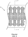
- the semiconductor substrate 12 is preferably a silicon semiconductor substrate 12 containing a plurality of fluid ejectors 14 such as piezoelectric devices or heater resistors formed on a device surface 28 of the substrate 12 as shown in the simplified illustration of FIG. 3 .
- FIGs. 3-5 illustrate a mask and method for forming the prior art flow feature layer 16 on the semiconductor substrate 12.
- the substrate 12 Prior to forming the flow feature layer 16 on the substrate 12, the substrate 12 is etched using a deep reactive ion etching (DRIE) process to form one or more fluid supply vias 24 therein.
- a thick film layer 34 is applied to the substrate 12 by dry laminating or spin coating the thick film layer 34 onto the device surface 28 of the substrate 12.
- the device surface of the substrate may be prepared to promote adhesion between the substrate 12 and the thick film layer 34 by plasma treating the device surface 28 with oxygen and/or silane before laminating or spin coating the thick film layer 34 to the substrate 12.
- DRIE deep reactive ion etching
- Silane compounds that are compatible with the components of the photoresist formulation typically have a functional group capable of reacting with at least one member selected from the group consisting of a multifunctional epoxy compound, a difunctional epoxy compound and a photoinitiator.
- an adhesion enhancing agent may be a silane with an epoxide functional group such as a glycidoxy-alkyltrialkoxysilane, e.g., gammaglycidoxypropyltrimethoxysilane.
- the adhesion enhancing agent is preferably present in an amount ranging from about 0.5 to about 2 weight percent and preferably from about 1.0 to about 1.5 weight percent based on total weight of the cured resin, including all ranges subsumed therein.
- Adhesion enhancing agents are defined to mean organic materials soluble in the photoresist composition which assist the film forming and adhesion characteristics of the thick film layer 34 on the device surface 28 of the substrate 12.
- the thick film layer 34 is then exposed to UV radiation 42 through a mask 36 having an opaque area 38 and a transparent area 40 as shown in FIGs. 4 and 5 .
- the thick film layer 34 is heated to cross-link the UV exposed areas of the thick film layer 34 under the transparent areas 40 of the mask 36.
- the thick film layer 34 is not developed at this stage of the process.
- the nozzle plate 18 is laminated to the exposed and undeveloped thick film layer 34 using a compression roll laminator. Adhesion may be promoted between the thick film layer 34 and the nozzle plate 18 by treating the surface 32 of the thick film layer 34 with oxygen plasma and a forming gas and/or silane.
- the nozzle plate 18 is exposed to UV radiation through a mask, having opaque areas corresponding to nozzle hole areas. After exposing the nozzle plate 18 to UV radiation, the nozzle plate 18 and thick film layer 34 are developed simultaneously using a photoresist developer. The substrate 12 containing the exposed thick film layer 34 and nozzle plate 18 is placed in a developer bath using megasonic agitation to dissolve the uncross-linked materials in both the thick film layer 34 and nozzle plate 18 so that the un-crosslinked material from the thick film layer 34 is dissolved through the previously formed via 24 and the un-crosslinked material from the nozzle plate 18 is dissolved through nozzle holes 20 in the nozzle plate 18.
- Illustrative developers used in the developer bath include, for example, butyl cellosolve acetate, cyclohexanone, methyl ethyl ketone, a xylene and butyl cellosolve acetate mixture, and C1-6 acetates like butyl acetate, or a combination of two or more of the foregoing.
- the flow feature layer 16 has elongate, relatively narrow fingers 30 that form the fluid channels 22 leading to the fluid chambers 26. Since the surface 32 of the flow feature layer 16 to which the nozzle plate 18 is attached is narrow in the area of the fingers 30, there is often adhesion failure between the nozzle plate 18 and the flow feature layer 16 in the area of the fingers 30.
- imaging masks and methods for improving the adhesion between a nozzle plate and a flow feature layer are illustrated.
- a mask 50 having opaque areas 52 and gray scale areas 54 is used to provide a roughened surface 56 of a negative photoresist thick film layer 58.
- Gray scale photoimaging uses sub-resolution pixels on the surface of the mask. The sub-resolution pixels manipulate the actinic light source by means of attenuating the overall light intensity for initiating a chemical reaction in the photoresist material of the thick film layer 58.
- the gray scale areas of the mask 50 reduce transmission of ultraviolet light 42 through the mask by up to 50 % thereby reducing the amount of cross-linking of the negative photoresist material in the gray scale areas 54, particularly along the fingers 30, as described above.
- the nozzle plate 18 is heat laminated to the surface 56 of the thick film layer 58 using pressure and heat.
- the increased surface area greatly improves adhesion between the nozzle plate 18 and the thick film layer 58.
- the resulting ejection head 60 has improved adhesion of the nozzle plate 18 to the thick film layer 58 in the area of the fingers 30 even in the absence of plasma surface treatment of the thick film layer 58 and coating the thick film layer with a silane adhesion agent.
- a mask 70 containing small solid metal particles such as chrome particles on the mask 70 are used as indicated by areas 72 while area 74 is opaque as with the other masks 36 and 50 described above.
- the opaque area 74 prevents crosslinking of the photoresist material in a thick film layer 76 in order to form the fluid channels 22 and fluid chambers 26.
- the small metal particles prevent UV radiation from impacting on portions of the surface 78 of the thick film layer 76 that causes such portions to remain un-crosslinked.
- the uncross-linked areas form a plurality of concavities 80 in the surface 78 of the thick film layer 76.
- the concavities 80 provide an increase surface area for improved adhesion of the nozzle plate 18 to the thick film layer 76.
- FIG. 11 illustrates a mask 90 according to another embodiment of the disclosure.
- the mask 90 includes a plurality of geometric-shaped opaque particles 92 that attenuate the radiation in order to form unresolved images on the surface of a thick film layer.
- the unresolved images on the surface of the thick film layer are removed during development of the thick film layer leaving geometric shapes on the surface which increase the surface area for increased mechanical interlocking between the nozzle plate and the thick film layer.
- the opaque areas 94 of the mask 90 provide the fluid channels 22 and fluid chambers 26 in the thick film layer.
- the plurality of geometric-shaped opaque particles can have a variety of shapes including, circles, triangles, rectangles, zig-zag lines, and the like.
Landscapes
- Physics & Mathematics (AREA)
- Engineering & Computer Science (AREA)
- Manufacturing & Machinery (AREA)
- General Physics & Mathematics (AREA)
- Spectroscopy & Molecular Physics (AREA)
- Particle Formation And Scattering Control In Inkjet Printers (AREA)
Abstract
Description
- The disclosure relates to improved fluid ejection heads and in particular to methods for improving adhesion of a nozzle plate to a flow feature layer of a fluid ejection head.
- Fluid jet ejection heads are used in a wide variety of application including, but not limited to, ink jet ejection heads, digital fluid dispensing devices, and pharmaceutical jet spray devices. Primary components of the fluid jet ejection heads include micro-electro-mechanical (MEMS) devices that is made from a silicon substrate and have metal and non-metal layers deposited thereon to provide electrically activated fluid ejectors. The fluid ejectors may be thermal fluid ejectors, bubble jet ejectors, or piezoelectric ejectors. A flow feature layer is applied to the MEMS device to direct fluid from a supply cartridge to the fluid ejectors. The flow feature layer includes fluid flow channels to direct fluid from a fluid supply via in the silicon substrate to fluid chambers containing the fluid ejectors. A nozzle plate is attached to the flow feature layer to provide ejection nozzles for ejecting fluid from the ejection head upon activation of the fluid ejectors.
- An area of the construction of the fluid jet ejection heads that remains problematic is the adhesion of the nozzle plate to the flow feature layer of the ejection head. Some surface areas of the flow feature layer to which the nozzle plate is attached are narrow and relatively smooth. A conventional method for attaching the nozzle plate to the flow feature layer is to laminate the nozzle plate to the flow feature layer after treating the exposed surface of the flow feature layer with oxygen plasma and coating the exposed surface with silane. However, even with oxygen plasma and the silane coating, adhesion of the nozzle plate to the narrow surface areas of the flow feature layer remains problematic. Furthermore, the steps of oxygen plasma treatment and silane coating of the flow feature layer are time consuming processes that increase production time and decrease production throughput. Accordingly, what is needed is a method for improving adhesion of the nozzle plate to the flow feature layer which does not adversely affect production time, and which is more cost effective to implement.
- Accordingly, an embodiment of the disclosure provides a fluid ejection head for a fluid jet ejection device. The fluid ejection head includes a silicon substrate containing at least one array of fluid ejectors deposited thereon. At least one fluid supply via is etched through the silicon substrate adjacent to the at least one array of fluid ejectors. A flow feature layer is attached to the silicon substrate. The flow feature layer contains at least one array of fluid chambers and fluid flow channels corresponding the at least one array of fluid ejectors for ejecting fluid to provide fluid from the at least one fluid supply via to fluid chambers. At least a portion of the flow feature layer has an attachment surface having improved surface adhesion characteristics. A nozzle plate containing nozzle holes is laminated to the flow feature layer to provide the fluid ejection head.
- In another embodiment there is provided a method for improving adhesion of a nozzle plate to a flow feature layer of a fluid ejection head. The method includes providing a silicon substrate having a device surface containing at least one array of fluid ejectors thereon. A photoresist material is spin-coated onto the device surface of the silicon substrate. The photoresist material is exposed to actinic radiation through a mask to provide the flow feature layer. The mask contains opaque areas defining a plurality of fluid flow channels and fluid chambers in the photoresist material and mask areas adjacent to the plurality of fluid flow channels and fluid chambers that provide improved surface adhesion characteristics surface area for increased adhesion between a developed surface of the photoresist material and a nozzle plate attached to the photoresist material.
- Another embodiment of the disclosure provides a method for making a fluid jet ejection head. The method includes providing a silicon substrate having a device surface containing at least one array of fluid ejectors thereon. A photoresist material is laminated or spin-coated onto the device surface of the silicon substrate. The photoresist material is exposed to actinic radiation through a mask to provide a flow feature layer. The mask contains opaque areas defining a plurality of fluid flow channels and fluid chambers in the photoresist material and mask areas adjacent to the plurality of fluid flow channels and fluid chambers that provide a surface area with improved surface adhesion characteristics for increased adhesion between a developed surface of the photoresist material and a nozzle plate attached to the photoresist material. A fluid supply via is etched in the silicon substrate. The photoresist material is developed to provide the plurality of fluid flow channels and fluid chambers therein and areas of improved surface adhesion characteristics. A nozzle plate is attached to the surface of the flow feature layer.
- In some embodiments, the flow feature layer comprises a negative photoresist material spin coated or laminated onto the silicon substrate.
- In some embodiments, the flow feature layer is imaged through a mask containing opaque areas and gray scale areas, wherein the gray scale areas provide a roughened attachment surface having the improved surface adhesion characteristics.
- In some embodiments, the flow feature layer is imaged through a mask containing opaque areas and areas containing chrome particles, wherein the areas containing chrome particles provide concavities on a portion of the surface of the flow feature layer whereby a surface area for attaching the nozzle plate to the flow feature layer has the improved surface adhesion characteristics.
- In some embodiments, the flow feature layer is imaged through a mask containing opaque areas and areas containing opaque geometric shapes, wherein the areas containing opaque geometric shapes provide a surface of the flow feature layer whereby a surface area for attaching the nozzle plate to the flow feature layer has the improved surface adhesion characteristics.
- In some embodiments, the mask areas adjacent to the plurality of fluid flow channels and fluid chambers contains gray scale areas that decrease an intensity of the actinic radiation by about 20 to about 50 %.
- In some embodiments, the mask areas adjacent to the plurality of fluid flow channels and fluid chambers comprise a plurality of opaque particles that cause concavities to be developed in the photoresist material that provide the improved surface adhesion characteristics.
- In some embodiments, the mask areas adjacent to the plurality of fluid flow channels and fluid chambers comprise a plurality of opaque geometric shapes that cause geometric patterns to be developed in the photoresist material to provide the improved surface adhesion characteristics.
- In some embodiments, the photoreist material comprises a negative photoresist material.
- In some embodiments, the nozzle plate is laminated to the surface of the flow feature layer in the absence of oxygen plasma treatment of the areas of the flow feature layer having the improved surface adhesion characteristics.
- In some embodiments, the nozzle plate is laminated to the surface of the flow feature layer in the absence of silane coating the areas of the flow feature layer having the improved surface adhesion characteristics.
- Advantages of the disclosed embodiments include, but are not limited to, improved adhesion of the nozzle plate to the flow feature layer, reduced ejection head processing time, reduced ejection head costs, and other benefits and advantages. The embodiments may be implemented without increasing the process steps required to fabricate ejection heads for fluid ejection devices. In some embodiments, process steps of oxygen plasma treatment of an exposed surface of the flow feature layer and coating with a silane adhesion agent may be eliminated.
-
-
FIG. 1 is a plan, cut-away view, not to scale, of a prior art fluid ejection head for a fluid ejection device. -
FIG. 2 is a perspective view, not to scale, of a portion of a semiconductor substrate containing a fluid via therein and a fluid flow layer attached to the substrate. -
FIG. 3 is a plan view, not to scale, of a portion of a prior art mask used for forming fluid flow channels and fluid chambers in a flow feature layer of the ejection head ofFIG. 1 . -
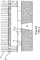
FIG. 4 is a schematic illustration, not to scale, of an imaging process for the flow feature layer of the fluid ejection head ofFIG. 1 . -
FIG. 5 is a cross-sectional, not to scale, of a portion of the prior art fluid ejection head ofFIG. 1 prior to developing the thick film layer and nozzle plate. -
FIG. 6 is a mask, not to scale, containing gray-scale areas for forming a flow feature layer of an ejection head according to a first embodiment of the disclosure. -
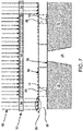
FIG. 7 is a schematic illustration, not to scale, of an imaging process for the flow feature layer using the mask ofFIG. 6 . -
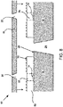
FIG. 8 is a cross-sectional view, not to scale, of a nozzle plate being attached to a surface of a flow feature layer made according to the imaging process ofFIG. 7 . -
FIG. 9 is a mask, not to scale, containing opaque particles for forming a flow feature layer of an ejection head according to a second embodiment of the disclosure. -
FIG. 10 is a schematic illustration, not to scale, of an imaging process for the flow feature layer using the mask ofFIG. 8 . -
FIG. 11 is a mask, not to scale, containing opaque geometric shapes for forming a flow feature layer of an ejection head according to a third embodiment of the disclosure. - With reference to
FIGs. 1-5 , there are shown simplified representations of portions of a priorart ejection head 10 containing asemiconductor substrate 12,fluid ejectors 14, aflow feature layer 16, and anozzle plate 18 containingnozzle holes 20 therein. Theflow feature layer 16 includesfluid channels 22 leading from a fluid supply via 24 in the semiconductor substrate to afluid chamber 26 containing thefluid ejectors 14. Thesemiconductor substrate 12 is preferably asilicon semiconductor substrate 12 containing a plurality offluid ejectors 14 such as piezoelectric devices or heater resistors formed on adevice surface 28 of thesubstrate 12 as shown in the simplified illustration ofFIG. 3 . Fluid supplied through one or morefluid supply vias 24 in thesemiconductor substrate 12 flows through thefluid channel 22 to afluid chamber 26 formed in theflow feature layer 16 where the fluid is caused to be ejected through anozzle hole 20 in thenozzle plate 18 when thefluid ejector 14 is activated. -
FIGs. 3-5 illustrate a mask and method for forming the prior artflow feature layer 16 on thesemiconductor substrate 12. Prior to forming theflow feature layer 16 on thesubstrate 12, thesubstrate 12 is etched using a deep reactive ion etching (DRIE) process to form one or morefluid supply vias 24 therein. Next athick film layer 34 is applied to thesubstrate 12 by dry laminating or spin coating thethick film layer 34 onto thedevice surface 28 of thesubstrate 12. The device surface of the substrate may be prepared to promote adhesion between thesubstrate 12 and thethick film layer 34 by plasma treating thedevice surface 28 with oxygen and/or silane before laminating or spin coating thethick film layer 34 to thesubstrate 12. Silane compounds that are compatible with the components of the photoresist formulation typically have a functional group capable of reacting with at least one member selected from the group consisting of a multifunctional epoxy compound, a difunctional epoxy compound and a photoinitiator. Such an adhesion enhancing agent may be a silane with an epoxide functional group such as a glycidoxy-alkyltrialkoxysilane, e.g., gammaglycidoxypropyltrimethoxysilane. When used, the adhesion enhancing agent is preferably present in an amount ranging from about 0.5 to about 2 weight percent and preferably from about 1.0 to about 1.5 weight percent based on total weight of the cured resin, including all ranges subsumed therein. Adhesion enhancing agents, as used herein, are defined to mean organic materials soluble in the photoresist composition which assist the film forming and adhesion characteristics of thethick film layer 34 on thedevice surface 28 of thesubstrate 12. - The
thick film layer 34 is then exposed toUV radiation 42 through amask 36 having anopaque area 38 and atransparent area 40 as shown inFIGs. 4 and5 . Thethick film layer 34 is heated to cross-link the UV exposed areas of thethick film layer 34 under thetransparent areas 40 of themask 36. Thethick film layer 34 is not developed at this stage of the process. - In the next step of the process, the
nozzle plate 18 is laminated to the exposed and undevelopedthick film layer 34 using a compression roll laminator. Adhesion may be promoted between thethick film layer 34 and thenozzle plate 18 by treating thesurface 32 of thethick film layer 34 with oxygen plasma and a forming gas and/or silane. - In order to provide
nozzle holes 20 in thenozzle plate 18, thenozzle plate 18 is exposed to UV radiation through a mask, having opaque areas corresponding to nozzle hole areas. After exposing thenozzle plate 18 to UV radiation, thenozzle plate 18 andthick film layer 34 are developed simultaneously using a photoresist developer. Thesubstrate 12 containing the exposedthick film layer 34 andnozzle plate 18 is placed in a developer bath using megasonic agitation to dissolve the uncross-linked materials in both thethick film layer 34 andnozzle plate 18 so that the un-crosslinked material from thethick film layer 34 is dissolved through the previously formed via 24 and the un-crosslinked material from thenozzle plate 18 is dissolved through nozzle holes 20 in thenozzle plate 18. Illustrative developers used in the developer bath include, for example, butyl cellosolve acetate, cyclohexanone, methyl ethyl ketone, a xylene and butyl cellosolve acetate mixture, and C1-6 acetates like butyl acetate, or a combination of two or more of the foregoing. - As seen in
FIG. 2 , theflow feature layer 16 has elongate, relativelynarrow fingers 30 that form thefluid channels 22 leading to thefluid chambers 26. Since thesurface 32 of theflow feature layer 16 to which thenozzle plate 18 is attached is narrow in the area of thefingers 30, there is often adhesion failure between thenozzle plate 18 and theflow feature layer 16 in the area of thefingers 30. - With reference not to
FIGs. 6-11 , imaging masks and methods for improving the adhesion between a nozzle plate and a flow feature layer are illustrated. In a first embodiment, (FIGs. 6-8 ), amask 50 havingopaque areas 52 andgray scale areas 54 is used to provide a roughenedsurface 56 of a negative photoresistthick film layer 58. Gray scale photoimaging uses sub-resolution pixels on the surface of the mask. The sub-resolution pixels manipulate the actinic light source by means of attenuating the overall light intensity for initiating a chemical reaction in the photoresist material of thethick film layer 58. The result of attenuating the light intensity is that small features are formed on thesurface 56 of thethick film layer 58 that increase the surface area of thesurface 56 of the thick film layer. In some embodiments, the gray scale areas of themask 50 reduce transmission ofultraviolet light 42 through the mask by up to 50 % thereby reducing the amount of cross-linking of the negative photoresist material in thegray scale areas 54, particularly along thefingers 30, as described above. - In
FIG. 8 , thenozzle plate 18 is heat laminated to thesurface 56 of thethick film layer 58 using pressure and heat. The increased surface area greatly improves adhesion between thenozzle plate 18 and thethick film layer 58. The resultingejection head 60 has improved adhesion of thenozzle plate 18 to thethick film layer 58 in the area of thefingers 30 even in the absence of plasma surface treatment of thethick film layer 58 and coating the thick film layer with a silane adhesion agent. - In another embodiment, illustrated in
FIGs. 9-10 , amask 70 containing small solid metal particles such as chrome particles on themask 70 are used as indicated byareas 72 whilearea 74 is opaque as with theother masks opaque area 74 prevents crosslinking of the photoresist material in athick film layer 76 in order to form thefluid channels 22 andfluid chambers 26. Likewise, the small metal particles prevent UV radiation from impacting on portions of thesurface 78 of thethick film layer 76 that causes such portions to remain un-crosslinked. When thethick film layer 76 is developed, the uncross-linked areas form a plurality ofconcavities 80 in thesurface 78 of thethick film layer 76. Like the previous embodiment, theconcavities 80 provide an increase surface area for improved adhesion of thenozzle plate 18 to thethick film layer 76. -
FIG. 11 illustrates amask 90 according to another embodiment of the disclosure. According to this embodiment, themask 90 includes a plurality of geometric-shapedopaque particles 92 that attenuate the radiation in order to form unresolved images on the surface of a thick film layer. Like the previous embodiment, the unresolved images on the surface of the thick film layer are removed during development of the thick film layer leaving geometric shapes on the surface which increase the surface area for increased mechanical interlocking between the nozzle plate and the thick film layer. Theopaque areas 94 of themask 90 provide thefluid channels 22 andfluid chambers 26 in the thick film layer. It will be appreciated that the plurality of geometric-shaped opaque particles can have a variety of shapes including, circles, triangles, rectangles, zig-zag lines, and the like.
Claims (18)
- A fluid ejection head (60) for a fluid jet ejection device comprising,a silicon substrate (12) containing at least one array of fluid ejectors (14) deposited thereon,at least one fluid supply via (24) etched through the silicon substrate (12) adjacent to the at least one array of fluid ejectors (14),a flow feature layer (58, 76) attached to the silicon substrate (12), the flow feature layer (58, 76) containing at least one array of fluid chambers (26) and fluid flow channels (22) corresponding the at least one array of fluid ejectors (14) for ejecting fluid to provide fluid from the at least one fluid supply via (24) to the fluid chambers (26), wherein at least a portion of the flow feature layer (58, 76) comprises an attachment surface (56, 78) having a surface area with improved surface adhesion characteristics, anda nozzle plate (18) containing nozzle holes (20) laminated to the flow feature layer (58, 76) to provide the fluid ejection head (60).
- The fluid ejection head (60) of claim 1, wherein the flow feature layer (58, 76) comprises a negative photoresist material spin coated onto the silicon substrate (12).
- The fluid ejection head (60) of claim 1, wherein the flow feature layer (58, 76) comprises a negative photoresist material laminated to the silicon substrate (12).
- The fluid ejection head (60) of claim 2, wherein the flow feature layer (58, 76) is imaged through a mask (50, 70, 90) containing opaque areas (52, 74, 94) and gray scale areas (54), wherein the gray scale areas (54) provide a roughened attachment surface (56, 78) having the improved surface adhesion characteristics.
- The fluid ejection head (60) of claim 2, wherein the flow feature layer (58, 76) is imaged through a mask (50, 70, 90) containing opaque areas (52, 74, 94) and areas (72) containing chrome particles, wherein the areas (72) containing chrome particles provide concavities (80) on a portion of the surface (56, 78) of the flow feature layer (58, 76) whereby a surface area for attaching the nozzle plate (18) to the flow feature layer (58, 76) has the improved surface adhesion characteristics.
- The fluid ejection head (60) of claim 2, wherein the flow feature layer (58, 76) is imaged through a mask (50, 70, 90) containing opaque areas (52, 74, 94) and areas (92) containing opaque geometric shapes, wherein the areas (92) containing opaque geometric shapes provide a surface (56, 78) of the flow feature layer (58, 76) whereby a surface area for attaching the nozzle plate (18) to the flow feature layer (58, 76) has the improved surface adhesion characteristics.
- A method for improving adhesion of a nozzle plate (18) to a flow feature layer (58, 76) of a fluid ejection head (60) comprising:providing a silicon substrate (12) having a device surface containing at least one array of fluid ejectors (14) thereon;spin-coating a photoresist material onto the device surface of the silicon substrate (12);exposing the photoresist material to actinic radiation (42) through a mask (50, 70, 90) to provide the flow feature layer (58, 76), wherein the mask (50, 70, 90) contains opaque areas (52, 74, 94) defining a plurality of fluid flow channels (22) and fluid chambers (26) in the photoresist material and mask areas adjacent to the plurality of fluid flow channels (22) and fluid chambers (26) that provide a surface area with improved surface adhesion characteristics for increased adhesion between a developed surface (56, 78) of the photoresist material and a nozzle plate (18) attached to the photoresist material.
- The method of claim 7, wherein the mask areas adjacent to the plurality of fluid flow channels (22) and fluid chambers (26) comprise gray scale areas (54) that decrease an intensity of the actinic radiation (42) by 20 to 50 %.
- The method of claim 7, wherein the mask areas adjacent to the plurality of fluid flow channels (22) and fluid chambers (26) comprise a plurality of opaque particles that cause concavities (80) to be developed in the photoresist material to provide the improved surface adhesion characteristics.
- The method of claim 7, wherein the mask areas adjacent to the plurality of fluid flow channels (22) and fluid chambers (26) comprise a plurality of opaque geometric shapes that cause geometric patterns to be developed in the photoresist material to provide the improved surface adhesion characteristics.
- The method of claim 7, wherein the photoresist material comprises a negative photoresist material.
- A method for making a fluid jet ejection head (60) comprising:providing a silicon substrate (12) having a device surface containing at least one array of fluid ejectors (14) thereon;laminating or spin-coating a photoresist material onto the device surface of the silicon substrate (12);exposing the photoresist material to actinic radiation (42) through a mask (50, 70, 90) to provide a flow feature layer (58, 76), wherein the mask (50, 70, 90) contains opaque areas (52, 74, 94) defining a plurality of fluid flow channels (22) and fluid chambers (26) in the photoresist material and mask areas adjacent to the plurality of fluid flow channels (22) and fluid chambers (26) that provide a surface area with improved surface adhesion characteristics for increased adhesion between a developed surface (56, 78) of the photoresist material and a nozzle plate (18) attached to the photoresist material;etching a fluid supply via (24) in the silicon substrate (12);developing the photoresist material to provide the plurality of fluid flow channels (22) and fluid chambers (26) therein and areas of improved surface adhesion characteristics; andattaching the nozzle plate (18) to the surface (56, 78) of the flow feature layer (58, 76).
- The method of claim 12, wherein the mask areas adjacent to the plurality of fluid flow channels (22) and fluid chambers (26) comprise gray scale areas (54) that decrease an intensity of the actinic radiation (42) by 20 to 50 %.
- The method of claim 12, wherein the mask areas adjacent to the plurality of fluid flow channels (22) and fluid chambers (26) comprise a plurality of opaque particles that cause concavities (80) to be developed in the photoresist material to provide the improved surface adhesion characteristics.
- The method of claim 12, wherein the mask areas adjacent to the plurality of fluid flow channels (22) and fluid chambers (26) comprise a plurality of opaque geometric shapes (92) that cause geometric patterns to be developed in the photoresist material to provide the improved surface adhesion characteristics.
- The method of claim 12, wherein the photoresist material comprises a negative photoresist material.
- The method of claim 12, wherein the nozzle plate (18) is laminated to the surface (56, 78) of the flow feature layer (58, 76) in the absence of oxygen plasma treatment of the areas of the flow feature layer (58, 76) having the improved surface adhesion characteristics.
- The method of claim 12, wherein the nozzle plate (18) is laminated to the surface (56, 78) of the flow feature layer (58, 76) in the absence of silane coating the areas of the flow feature layer (58, 76) having the improved surface adhesion characteristics.
Applications Claiming Priority (1)
| Application Number | Priority Date | Filing Date | Title |
|---|---|---|---|
| US17/193,731 US11926157B2 (en) | 2021-03-05 | 2021-03-05 | Photoresist imaging and development for enhanced nozzle plate adhesion |
Publications (1)
| Publication Number | Publication Date |
|---|---|
| EP4052914A1 true EP4052914A1 (en) | 2022-09-07 |
Family
ID=80447535
Family Applications (1)
| Application Number | Title | Priority Date | Filing Date |
|---|---|---|---|
| EP22157936.0A Pending EP4052914A1 (en) | 2021-03-05 | 2022-02-22 | Fluid ejection head, method for improving the same and method for making fluid jet ejection head |
Country Status (4)
| Country | Link |
|---|---|
| US (1) | US11926157B2 (en) |
| EP (1) | EP4052914A1 (en) |
| JP (1) | JP2022135994A (en) |
| CN (1) | CN115090432B (en) |
Citations (3)
| Publication number | Priority date | Publication date | Assignee | Title |
|---|---|---|---|---|
| JPH0592563A (en) * | 1991-10-03 | 1993-04-16 | Seiko Epson Corp | Ink jet head and method of manufacturing the same |
| US6409312B1 (en) * | 2001-03-27 | 2002-06-25 | Lexmark International, Inc. | Ink jet printer nozzle plate and process therefor |
| US20140218437A1 (en) * | 2011-06-06 | 2014-08-07 | Sicpa Holding Sa | Ink-jet print head comprising a layer made by a curable resin composition |
Family Cites Families (17)
| Publication number | Priority date | Publication date | Assignee | Title |
|---|---|---|---|---|
| JP3342095B2 (en) * | 1993-05-07 | 2002-11-05 | 株式会社ミクニ | Ultrasonic spray device |
| US7527357B2 (en) | 1997-07-15 | 2009-05-05 | Silverbrook Research Pty Ltd | Inkjet nozzle array with individual feed channel for each nozzle |
| US6310641B1 (en) * | 1999-06-11 | 2001-10-30 | Lexmark International, Inc. | Integrated nozzle plate for an inkjet print head formed using a photolithographic method |
| JP3998254B2 (en) | 2003-02-07 | 2007-10-24 | キヤノン株式会社 | Inkjet head manufacturing method |
| US7165831B2 (en) | 2004-08-19 | 2007-01-23 | Lexmark International, Inc. | Micro-fluid ejection devices |
| US7364268B2 (en) * | 2005-09-30 | 2008-04-29 | Lexmark International, Inc. | Nozzle members, compositions and methods for micro-fluid ejection heads |
| US8430484B2 (en) | 2010-06-28 | 2013-04-30 | Lexmark International, Inc. | Nozzle covering for ejection chips in micro-fluid applications |
| JP5585292B2 (en) * | 2010-08-16 | 2014-09-10 | 富士ゼロックス株式会社 | Light emitting element array with lens and print head |
| US9132639B2 (en) * | 2011-04-29 | 2015-09-15 | Funai Electric Co., Ltd. | Method for fabricating fluid ejection device |
| TWM430583U (en) * | 2011-11-09 | 2012-06-01 | Drytech Corp Ltd | Ultrasound oscillator with replaceable ultrasound oscillation components |
| WO2013129120A1 (en) * | 2012-02-29 | 2013-09-06 | 住友化学株式会社 | Liquid container, ultrasonic atomization device, and absorption body |
| CN104220176B (en) * | 2012-04-23 | 2017-04-12 | 空气芳香研究股份有限公司 | Atomiser system |
| BR112015005501A2 (en) * | 2012-09-12 | 2017-07-04 | Funai Electric Co | microfluid ejection head maintenance valves |
| US9101954B2 (en) | 2013-09-17 | 2015-08-11 | Applied Materials, Inc. | Geometries and patterns for surface texturing to increase deposition retention |
| GB201506748D0 (en) * | 2015-04-21 | 2015-06-03 | Personnel Hygiene Services Ltd | Fragrance dispenser |
| US9855566B1 (en) * | 2016-10-17 | 2018-01-02 | Funai Electric Co., Ltd. | Fluid ejection head and process for making a fluid ejection head structure |
| JP7009857B2 (en) | 2017-09-13 | 2022-01-26 | セイコーエプソン株式会社 | Liquid injection head, liquid injection device, and piezoelectric device |
-
2021
- 2021-03-05 US US17/193,731 patent/US11926157B2/en active Active
-
2022
- 2022-02-22 EP EP22157936.0A patent/EP4052914A1/en active Pending
- 2022-02-28 JP JP2022029520A patent/JP2022135994A/en active Pending
- 2022-03-01 CN CN202210196890.2A patent/CN115090432B/en active Active
Patent Citations (3)
| Publication number | Priority date | Publication date | Assignee | Title |
|---|---|---|---|---|
| JPH0592563A (en) * | 1991-10-03 | 1993-04-16 | Seiko Epson Corp | Ink jet head and method of manufacturing the same |
| US6409312B1 (en) * | 2001-03-27 | 2002-06-25 | Lexmark International, Inc. | Ink jet printer nozzle plate and process therefor |
| US20140218437A1 (en) * | 2011-06-06 | 2014-08-07 | Sicpa Holding Sa | Ink-jet print head comprising a layer made by a curable resin composition |
Also Published As
| Publication number | Publication date |
|---|---|
| CN115090432B (en) | 2024-06-14 |
| CN115090432A (en) | 2022-09-23 |
| US11926157B2 (en) | 2024-03-12 |
| US20220281224A1 (en) | 2022-09-08 |
| JP2022135994A (en) | 2022-09-15 |
Similar Documents
| Publication | Publication Date | Title |
|---|---|---|
| EP3312011B1 (en) | Fluid ejection head and method for making fluid ejection head | |
| US9873255B2 (en) | Liquid ejection head and method of manufacturing the same | |
| JPS5919168A (en) | Ink jet recording head | |
| CN104669795B (en) | The manufacture method of liquid discharging head | |
| CN102596575B (en) | Method for manufacturing liquid ejection head | |
| KR101012898B1 (en) | Liquid discharge head manufacturing method | |
| US20190077156A1 (en) | Method of manufacturing a liquid ejection head | |
| JP5653181B2 (en) | Hydrophilic film forming method, hydrophilic film, ink jet recording head manufacturing method, and ink jet recording head | |
| JP6478741B2 (en) | Method for manufacturing liquid discharge head | |
| US11926157B2 (en) | Photoresist imaging and development for enhanced nozzle plate adhesion | |
| US20240173977A1 (en) | Photoresist imaging and development for enhanced nozzle plate adhesion | |
| US11465418B2 (en) | Manufacturing method for structure and manufacturing method for liquid ejection head | |
| JP7134831B2 (en) | Manufacturing method of liquid ejection head | |
| KR101376402B1 (en) | Liquid discharge head manufacturing method | |
| JP2017064930A (en) | Method for manufacturing liquid discharge head | |
| JPH0698773B2 (en) | Inkjet head manufacturing method | |
| US8883404B2 (en) | Process for producing a liquid ejection head | |
| JP6373013B2 (en) | Method for manufacturing liquid discharge head and liquid discharge head | |
| JPH0712662B2 (en) | Method for manufacturing ink jet recording head | |
| JPH091801A (en) | Ink jet recording head and method of manufacturing the same | |
| JPS591269A (en) | Manufacture of ink jet recording head | |
| JPH08267766A (en) | Liquid jet recording head manufacturing method and liquid jet recording head according to the method | |
| JP2002264340A (en) | Method of manufacturing ink jet recording head and ink jet recording head by the manufacturing method |
Legal Events
| Date | Code | Title | Description |
|---|---|---|---|
| PUAI | Public reference made under article 153(3) epc to a published international application that has entered the european phase |
Free format text: ORIGINAL CODE: 0009012 |
|
| STAA | Information on the status of an ep patent application or granted ep patent |
Free format text: STATUS: THE APPLICATION HAS BEEN PUBLISHED |
|
| AK | Designated contracting states |
Kind code of ref document: A1 Designated state(s): AL AT BE BG CH CY CZ DE DK EE ES FI FR GB GR HR HU IE IS IT LI LT LU LV MC MK MT NL NO PL PT RO RS SE SI SK SM TR |
|
| STAA | Information on the status of an ep patent application or granted ep patent |
Free format text: STATUS: REQUEST FOR EXAMINATION WAS MADE |
|
| 17P | Request for examination filed |
Effective date: 20230118 |
|
| RBV | Designated contracting states (corrected) |
Designated state(s): AL AT BE BG CH CY CZ DE DK EE ES FI FR GB GR HR HU IE IS IT LI LT LU LV MC MK MT NL NO PL PT RO RS SE SI SK SM TR |
|
| STAA | Information on the status of an ep patent application or granted ep patent |
Free format text: STATUS: EXAMINATION IS IN PROGRESS |
|
| 17Q | First examination report despatched |
Effective date: 20231108 |
|
| 19U | Interruption of proceedings before grant |
Effective date: 20241024 |