EP4050492A1 - Timing detection and correction method for a slave device in an io-link communication and slave device of an io-link communication - Google Patents
Timing detection and correction method for a slave device in an io-link communication and slave device of an io-link communication Download PDFInfo
- Publication number
- EP4050492A1 EP4050492A1 EP21159590.5A EP21159590A EP4050492A1 EP 4050492 A1 EP4050492 A1 EP 4050492A1 EP 21159590 A EP21159590 A EP 21159590A EP 4050492 A1 EP4050492 A1 EP 4050492A1
- Authority
- EP
- European Patent Office
- Prior art keywords
- timing
- slave device
- data transmission
- master
- correction method
- Prior art date
- Legal status (The legal status is an assumption and is not a legal conclusion. Google has not performed a legal analysis and makes no representation as to the accuracy of the status listed.)
- Granted
Links
Images


Classifications
-
- G—PHYSICS
- G06—COMPUTING OR CALCULATING; COUNTING
- G06F—ELECTRIC DIGITAL DATA PROCESSING
- G06F13/00—Interconnection of, or transfer of information or other signals between, memories, input/output devices or central processing units
- G06F13/38—Information transfer, e.g. on bus
- G06F13/40—Bus structure
- G06F13/4004—Coupling between buses
- G06F13/4027—Coupling between buses using bus bridges
- G06F13/405—Coupling between buses using bus bridges where the bridge performs a synchronising function
-
- H—ELECTRICITY
- H04—ELECTRIC COMMUNICATION TECHNIQUE
- H04L—TRANSMISSION OF DIGITAL INFORMATION, e.g. TELEGRAPHIC COMMUNICATION
- H04L7/00—Arrangements for synchronising receiver with transmitter
- H04L7/0008—Synchronisation information channels, e.g. clock distribution lines
- H04L7/0012—Synchronisation information channels, e.g. clock distribution lines by comparing receiver clock with transmitter clock
-
- H—ELECTRICITY
- H04—ELECTRIC COMMUNICATION TECHNIQUE
- H04J—MULTIPLEX COMMUNICATION
- H04J3/00—Time-division multiplex systems
- H04J3/02—Details
- H04J3/06—Synchronising arrangements
- H04J3/0635—Clock or time synchronisation in a network
- H04J3/0638—Clock or time synchronisation among nodes; Internode synchronisation
- H04J3/0658—Clock or time synchronisation among packet nodes
- H04J3/0661—Clock or time synchronisation among packet nodes using timestamps
- H04J3/0667—Bidirectional timestamps, e.g. NTP or PTP for compensation of clock drift and for compensation of propagation delays
-
- G—PHYSICS
- G05—CONTROLLING; REGULATING
- G05B—CONTROL OR REGULATING SYSTEMS IN GENERAL; FUNCTIONAL ELEMENTS OF SUCH SYSTEMS; MONITORING OR TESTING ARRANGEMENTS FOR SUCH SYSTEMS OR ELEMENTS
- G05B19/00—Program-control systems
- G05B19/02—Program-control systems electric
- G05B19/04—Program control other than numerical control, i.e. in sequence controllers or logic controllers
- G05B19/042—Program control other than numerical control, i.e. in sequence controllers or logic controllers using digital processors
- G05B19/0421—Multiprocessor system
-
- G—PHYSICS
- G06—COMPUTING OR CALCULATING; COUNTING
- G06F—ELECTRIC DIGITAL DATA PROCESSING
- G06F13/00—Interconnection of, or transfer of information or other signals between, memories, input/output devices or central processing units
- G06F13/38—Information transfer, e.g. on bus
- G06F13/382—Information transfer, e.g. on bus using universal interface adapter
- G06F13/385—Information transfer, e.g. on bus using universal interface adapter for adaptation of a particular data processing system to different peripheral devices
-
- G—PHYSICS
- G06—COMPUTING OR CALCULATING; COUNTING
- G06F—ELECTRIC DIGITAL DATA PROCESSING
- G06F13/00—Interconnection of, or transfer of information or other signals between, memories, input/output devices or central processing units
- G06F13/38—Information transfer, e.g. on bus
- G06F13/42—Bus transfer protocol, e.g. handshake; Synchronisation
- G06F13/4204—Bus transfer protocol, e.g. handshake; Synchronisation on a parallel bus
- G06F13/4208—Bus transfer protocol, e.g. handshake; Synchronisation on a parallel bus being a system bus, e.g. VME bus, Futurebus, Multibus
- G06F13/4213—Bus transfer protocol, e.g. handshake; Synchronisation on a parallel bus being a system bus, e.g. VME bus, Futurebus, Multibus with asynchronous protocol
-
- G—PHYSICS
- G06—COMPUTING OR CALCULATING; COUNTING
- G06F—ELECTRIC DIGITAL DATA PROCESSING
- G06F13/00—Interconnection of, or transfer of information or other signals between, memories, input/output devices or central processing units
- G06F13/38—Information transfer, e.g. on bus
- G06F13/42—Bus transfer protocol, e.g. handshake; Synchronisation
- G06F13/4265—Bus transfer protocol, e.g. handshake; Synchronisation on a point to point bus
- G06F13/4273—Bus transfer protocol, e.g. handshake; Synchronisation on a point to point bus using a clocked protocol
-
- G—PHYSICS
- G06—COMPUTING OR CALCULATING; COUNTING
- G06F—ELECTRIC DIGITAL DATA PROCESSING
- G06F13/00—Interconnection of, or transfer of information or other signals between, memories, input/output devices or central processing units
- G06F13/38—Information transfer, e.g. on bus
- G06F13/42—Bus transfer protocol, e.g. handshake; Synchronisation
- G06F13/4265—Bus transfer protocol, e.g. handshake; Synchronisation on a point to point bus
- G06F13/4278—Bus transfer protocol, e.g. handshake; Synchronisation on a point to point bus using an embedded synchronisation
-
- G—PHYSICS
- G06—COMPUTING OR CALCULATING; COUNTING
- G06F—ELECTRIC DIGITAL DATA PROCESSING
- G06F13/00—Interconnection of, or transfer of information or other signals between, memories, input/output devices or central processing units
- G06F13/38—Information transfer, e.g. on bus
- G06F13/42—Bus transfer protocol, e.g. handshake; Synchronisation
- G06F13/4282—Bus transfer protocol, e.g. handshake; Synchronisation on a serial bus, e.g. I2C bus, SPI bus
- G06F13/4291—Bus transfer protocol, e.g. handshake; Synchronisation on a serial bus, e.g. I2C bus, SPI bus using a clocked protocol
-
- H—ELECTRICITY
- H04—ELECTRIC COMMUNICATION TECHNIQUE
- H04L—TRANSMISSION OF DIGITAL INFORMATION, e.g. TELEGRAPHIC COMMUNICATION
- H04L12/00—Data switching networks
- H04L12/28—Data switching networks characterised by path configuration, e.g. LAN [Local Area Networks] or WAN [Wide Area Networks]
- H04L12/40—Bus networks
- H04L12/40006—Architecture of a communication node
- H04L12/40013—Details regarding a bus controller
-
- H—ELECTRICITY
- H04—ELECTRIC COMMUNICATION TECHNIQUE
- H04L—TRANSMISSION OF DIGITAL INFORMATION, e.g. TELEGRAPHIC COMMUNICATION
- H04L7/00—Arrangements for synchronising receiver with transmitter
- H04L7/04—Speed or phase control by synchronisation signals
- H04L7/10—Arrangements for initial synchronisation
-
- G—PHYSICS
- G05—CONTROLLING; REGULATING
- G05B—CONTROL OR REGULATING SYSTEMS IN GENERAL; FUNCTIONAL ELEMENTS OF SUCH SYSTEMS; MONITORING OR TESTING ARRANGEMENTS FOR SUCH SYSTEMS OR ELEMENTS
- G05B2219/00—Program-control systems
- G05B2219/20—Pc systems
- G05B2219/22—Pc multi processor system
- G05B2219/2231—Leader-follower
-
- H—ELECTRICITY
- H04—ELECTRIC COMMUNICATION TECHNIQUE
- H04L—TRANSMISSION OF DIGITAL INFORMATION, e.g. TELEGRAPHIC COMMUNICATION
- H04L25/00—Baseband systems
- H04L25/02—Details ; arrangements for supplying electrical power along data transmission lines
- H04L25/0262—Arrangements for detecting the data rate of an incoming signal
Definitions
- the invention relates to a timing detection and correction method for a slave device in an IO-Link communication, wherein a master device and the slave device operate on a common basic timing.
- the invention further relates to a slave device of an IO-Link communication, wherein a master device and the slave device operate on a common basic timing.
- IO-Link is a short distance industrial communications networking standard (IEC 61131-9). The communication via IO-Link is bidirectional, digital, point-to-point and wired or wireless. IO-Link is for example used for connecting digital sensors and actuators in industrial applications.
- An IO-Link comprises a master device and at least one slave device, i.e. sensor or actuator.
- the master device provides an interface to higher-lever controller (PLC) and controls, particularly initiates, the communication with the slave devices.
- PLC higher-lever controller
- the IO-Link communication between the master device and the at least one slave device is based on a Universal Asynchronous Receiver Transmitter (UART) communication.
- UART Universal Asynchronous Receiver Transmitter
- a Universal Asynchronous Receiver Transmitter (UART) communication is an asynchronous serial communication in which the data format and transmission speeds are configurable.
- a major design aspect and requirement for UART communications - being asynchronous - is the timing accuracy between the master device and the slave device.
- the timing is for example defined by an agreed baud rate, wherein the master device and the slave device use crystal-based timing references or oscillators.
- crystal-based timing references or oscillators can not provide the required timing accuracy over the full temperature range and external crystal-based timing references require additional space.
- the object is solved by a time detection and correction method for a slave device in an IO-Link communication, wherein a master device and the slave device operate on a common basic timing, comprising the steps of:
- the master device and the slave device of the communication operate on a common basic timing.
- the slave device for example comprises a UART module to detect the INIT request sent from the master device during communication setup, as known in the prior art. To improve the timing accuracy the slave device, particularly the UART module, analyses the received INIT request and calculates the actual timing of the master device from the received INIT request. Since the master device and the slave device operate on a common basic timing the slave device has knowledge about the basic timing and on that basis the slave device can calculate the actual timing from the received INIT request by detecting differences to the expected basic timing.
- the initial timing of the slave device which bases on the common basic timing, is corrected to an actual timing based on the calculated actual timing of the master device. Since the initial timing of the slave device is corrected to the actual timing of the master device based on the received INIT request sent by the master device, the slave device can use an internal oscillator as timing reference for the common basic timing. Although such an oscillator does not provide the necessary accuracy, particularly over a high temperature range, the method according to the invention improves the accuracy based on the actual timing of the master device calculated from the received INIT request. Thus, using the method according to the invention the slave device can use an oscillator timing reference and at the same time provide the necessary timing accuracy for the protocol communication.
- the common basic timing is defined as a baud-rate and the correction of the initial timing of the slave device is based on a baud rate offset.
- the baud rate defines the speed of communication over a data channel in telecommunications or electronics.
- the unit for the baud rate is symbols per second or pulses per second.
- the baud rate offset defines how the initial timing, i.e. the initial baud rate, has to be corrected (amended) to correspond to the actual timing, i.e. actual baud rate, of the master device.
- the method further comprises the step of continuously tracking the actual timing of the master device and correcting the actual timing of the slave device.
- the timing of the slave device is not only corrected at the beginning of the communication, i.e. by correcting the initial timing of the slave device, but is continuously corrected by tracking the actual timing of the master device and correcting the actual timing of the slave device.
- the continuously tracking of the actual timing of the master device comprises the step of calculating the actual timing of the master device from at least one received data transmission at the slave device.
- the slave instead of analysing the INIT request sent by the master during communication setup the slave analyses the regular received data transmission to continuously correct the actual timing of the slave device.
- the step of calculating the actual timing of the master device from the at least one received data transmission at the slave device is performed after each received data transmission or in regular intervals.
- the step of calculating the actual timing of the master device from a received data transmission at the slave device is performed after each received data transmission or in regular intervals.
- the actual timing of the slave device is corrected after the end of one or more complete master telegrams, wherein one master telegram comprises two or more data transmissions.
- the first master telegram can comprise the INIT request and one or more data transmissions.
- the slave device receives multiple data transmissions respectively the INIT request and one or more data transmissions from the master device in a so-called master telegram.
- the slave device corrects the timing based on the analysis of the data transmissions respectively the analysis of the INIT request and data transmissions in the master telegram.
- the slave device can prepare a response to the master telegram and send the response to the master device using the corrected actual timing of the slave device.
- the correction of the actual timing of the slave device bases on low-pass filtering multiple data transmission of one or more master telegrams.
- the first master telegram includes the INIT request, which can also be considered during low-pass filtering.
- the step of calculating the actual timing of the master device from the received INIT request and/or the received data transmission comprises the step of extracting timing information from the received INIT request and/or the received data transmission.
- the step of extracting timing information from the received INIT request and/or the received data transmission bases for example on an analysis of the bits in the INIT request and/or the received data transmission.
- the step of extracting the timing information from the received INIT request and/or from the received data transmission comprises the step of detecting rising and/or falling edges in the INIT request and/or the received data transmission. By calculating times between certain rising and/or falling edge of bits in the INIT request and/or the received data transmission the slave device can calculate the actual timing of the master.
- the step of extracting timing information from the received INIT request and/or the received data transmission is performed by a hardware component of the slave device.
- the extraction of timing information from received INIT request and/or the received data transmission can be easily implemented by a hardware component, for example by detecting rising and/or falling edge of bits in the received INIT request and/or the received data transmission using a comparator.
- the hardware component further provides a high accuracy.
- the step of calculating the actual timing of the master device from the received INIT request and/or the received data transmission is performed by a software component of the slave device, wherein the software component processes the timing information extracted from the received INIT request and/or the received data transmission.
- the software component has the advantage that the algorithm used to calculate actual timing from the timing information extracted from the received INIT request and/or the received data transmission can be easily amended, optimized and/or replaced.
- the initial timing and/or actual timing of the slave device is only corrected if a certain threshold is exceeded.
- a certain threshold is exceeded.
- the threshold level can be for example parametrized or adaptive, i.e. the threshold can depend on certain parameters or be adapted.
- the step of calculating the actual timing of the master device from the received INIT request and/or calculating the actual timing of the master device from at least one received data transmission comprises the step of counting clock pulses in the INIT request, the at least one data transmission and/or in master telegrams.
- the slave device of the IO-Link communication comprises at least one Universal Asynchronous Receiver Transmitter (UART) module implementing the methods steps of:
- the slave device of the IO-Link communication comprises multiple Universal Asynchronous Receiver Transmitter (UART) modules each implementing the aforementioned method steps and having different initial timing settings.
- UART Universal Asynchronous Receiver Transmitter
- the IO-Link slave device has multiple UART modules, each configured to a different initial timing.
- the slave device comprises four UART modules with different initial timing distributed over +/-5 %. Due to the different initial timing settings the chances increase that one UART module correctly receives the INIT request sent from the master device during communication setup. Afterwards this UART module is used for the IO-Link communication. If the number of UART modules is increased, it is possible to detect the INIT request in a wider timing range.
- the object is further solved by a slave device of an IO-Link communication, wherein a master device and the slave device operate on a common basic timing, wherein the slave device comprises at least one Universal Asynchronous Receiver Transmitter module that implements the method according to the invention.
- the slave device can comprise specific hardware and/or software to implement the inventive method.
- the slave device is implemented in an integrated circuit without any external components like e.g. crystal based timing devices.
- the integrated circuit can comprise a memory for storing software components of the slave device.
- the slave device comprises multiple Universal Asynchronous Receiver Transmitter modules having different initial timing settings and each implementing the method according to the invention.
- the IO-Link slave device has multiple UART modules, each configured to a different initial timing.
- the slave device comprises four UART modules with different initial timing distributed over +/- 5 %. Due to the different initial timing settings the chances increase that one UART module correctly receives the INIT request sent from the master device during communication setup. Afterwards this UART module is used for the IO-Link communication. If the number of UART modules is increased, it is possible to detect the INIT request in a wider timing range.
- Fig. 1 shows a flow chart of a first embodiment of a timing and detection method for a slave device in an IO-Link communication.
- the IO-Link communication is asynchronous, wherein a master device and the slave device operate on a common basic timing. In an asynchronous communication there is no common timing reference for the master device and the slave device slave.
- the timing is for example defined by an agreed baud rate, wherein the master device and the slave device use crystal-based timing references or oscillators.
- a major design aspect and requirement for IO-Link communications - being asynchronous - is the timing accuracy between the master device and the slave device.
- the slave device detects the actual timing of the master device and corrects its initial timing to the actual timing of the slave device.
- the slave device continuously tracks the actual timing of the master device and corrects its actual timing to the actual timing of the master device.
- the inventive methods is started, i.e. the slave device is ready for a communication and is listening to the communication channel. This is for example initiated by the master device by sending a wake-up request (WURQ) to the slave device.
- WURQ wake-up request
- the master device After the slave device is ready for communication and listening to the communication channel the master device sends an INIT request to the slave device via the communication channel to setup the communication between the master device and the slave device.
- the slave device detects the INIT request sent from the master.
- the slave device calculates the actual timing of the master device. Before sending a response to the master device the slave device corrects its initial timing to the calculated actual timing of the master device, thereby increasing the timing accuracy between the master device and the slave device.
- the slave device After the communication between the master device and the slave device has been setup, the slave device continuously tracks the actual timing of the master device and corrects its actual timing. This is achieved by receiving data transmissions from the master device at the slave device and calculating the actual timing of the master device from the received data transmission at the slave device. This can be for example performed after each received data transmission or after a predefined number of data transmissions.
- the step of calculating the actual timing of the master device from the received INIT request and/or the received data transmission preferably comprises the step of extracting timing information from the received INIT request and/or the received data transmission.
- the extracting of the timing information from the received INIT request and/or from the received data transmission for example comprises the step of detecting rising and/or falling edges in the INIT request and/or the received data transmission. The difference between detected rising and/or falling edges in the INIT request and/or the received data transmission is used to calculate the actual timing of the master device.
- the step of calculating the actual timing of the master device from the received INIT request and/or calculating the actual timing of the master device from at least one received data transmission comprises the step of counting clock pulses in the INIT request or at least one data transmission. For example, clock pulses between predefines rising and/or falling edges in the INIT request or at least one data transmission are counted.
- the step of extracting timing information from the received INIT request and/or the received data transmission is performed by a hardware component of the slave device.
- a hardware comparator detects rising and/or falling edges in the INIT request and/or the received data transmission.
- the step of calculating the actual timing of the master device from the received INIT request and/or the received data transmission is performed by a software component of the slave device, wherein the software component processes the timing information extracted from the received INIT request and/or the received data transmission.
- the initial timing and/or actual timing of the slave device is only corrected if a certain threshold is exceeded.
- the timing of the slave device is not corrected.
- the method according to the invention is executed by the slave device until the communication with the master device ends.
- the slave device of the IO-Link communication comprises multiple Universal Asynchronous Receiver Transmitter modules each implementing the steps of:
- the multiple Universal Asynchronous Receiver Transmitter modules each have different initial timing settings. Thereby, it is more likely that the INIT request sent by the master device during communication setup is correctly received by at least one Universal Asynchronous Receiver Transmitter module.
- the module correctly receiving the INIT request is chose for further communication between the slave device and master device. If more than one module correctly receives the INIT request preferably the fastest module is chosen.
- Fig. 2 shows a flow chart of a second embodiment of a timing and detection method for a slave device in an IO-Link communication.
- the second embodiment shown in Fig. 2 differs from the first embodiment shown in Fig. 1 in that the actual timing of the slave device is corrected after the end of one or more complete master telegrams.
- a master telegrams comprises two or more data transmissions or the INIT request and at least one data transmission.
- the slave device can calculate the actual timing of the master device from the received master telegram, i.e. the INIT request and the one or more data transmission respectively the two or more data transmissions.
- the correction of the actual timing of the slave device can e.g. base on low-pass filtering multiple data transmission of one or more master telegrams.
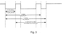
- Fig. 3 shows a signal diagram of an INIT request of an IO-Link communication and the extracting of timing information from the received INIT request.
- the Telegram-Counter counts clock pulses from the first falling edge in the protocol until the end of the protocol.
- the protocol is the INIT request or data transmission according to the first embodiment shown in Fig. 1 or the data telegram according to the second embodiment shown in Fig. 2 .
- the clock pulses are generated by the timing reference of the slave device.
- the Bit_Time_Counter counts the number of nominal clock pulses per configured Bit_Time.
- the configured Bit_Time depends on the common basic timing, particularly an agreed baud-rate between the master device and the slave device.
- the Bit_Time_Counter rolls over when bit_time_clocks value is reached.
- the Bit_Time_Counter triggers a count pulse for Bit_Num_Counter at about 50 % of Bit_Time to account for early/late arrival of next edge.
- the Bit_Num_Counter counts elapsed bit times from first falling edge in protocol based on ticks triggered by Bit_Time_Counter.
- Telegram_Counter is stored in register ct_first_rising and the value of Bit_Num_Counter is stored in register nbit_first rising.
- Telegram_Counter As soon as a falling edge is detected in the protocol after the first falling edge the value of Telegram_Counter is stored in register ct_falling and the value of Bit_Num_Counter is stored in register nbit_falling. This is repeated until the end of the protocol.
- Telegram_Counter As soon as a rising edge is detected in the protocol after the first rising edge the value of Telegram_Counter is stored in register ct_rising and the value of Bit_Num_Counter is stored in register nbit_rising. This is repeated until the end of the protocol.
- the acquired timing values are illustrated in Fig. 3 .
- the slave device for example checks if the timing is within certain limits defined by a threshold.
- the threshold is for example defined by register x_counts.
- the slave device continues to extract the above timing information from received data transmissions (protocols).
- bit_time_clock * nbit_rising + pulse_asymmetry ⁇ ct_rising ⁇ x_counts then increase bit_time_clock else if bit_time_clock * nbit_rising + pulse_asymmetry > ct_rising + x_counts then decrease bit_time_clock else no change.
Landscapes
- Engineering & Computer Science (AREA)
- Theoretical Computer Science (AREA)
- Physics & Mathematics (AREA)
- General Physics & Mathematics (AREA)
- General Engineering & Computer Science (AREA)
- Computer Networks & Wireless Communication (AREA)
- Signal Processing (AREA)
- Automation & Control Theory (AREA)
- Computer Hardware Design (AREA)
- Communication Control (AREA)
- Synchronisation In Digital Transmission Systems (AREA)
- Information Transfer Systems (AREA)
Abstract
Description
- The invention relates to a timing detection and correction method for a slave device in an IO-Link communication, wherein a master device and the slave device operate on a common basic timing. The invention further relates to a slave device of an IO-Link communication, wherein a master device and the slave device operate on a common basic timing.
- IO-Link is a short distance industrial communications networking standard (IEC 61131-9). The communication via IO-Link is bidirectional, digital, point-to-point and wired or wireless. IO-Link is for example used for connecting digital sensors and actuators in industrial applications. An IO-Link comprises a master device and at least one slave device, i.e. sensor or actuator. The master device provides an interface to higher-lever controller (PLC) and controls, particularly initiates, the communication with the slave devices. The IO-Link communication between the master device and the at least one slave device is based on a Universal Asynchronous Receiver Transmitter (UART) communication.
- A Universal Asynchronous Receiver Transmitter (UART) communication is an asynchronous serial communication in which the data format and transmission speeds are configurable. A major design aspect and requirement for UART communications - being asynchronous - is the timing accuracy between the master device and the slave device. The timing is for example defined by an agreed baud rate, wherein the master device and the slave device use crystal-based timing references or oscillators. However, internal oscillators can not provide the required timing accuracy over the full temperature range and external crystal-based timing references require additional space.
- It is therefore an object of the present invention to enhance the timing accuracy between the master device and the slave device of an IO-Link communication.
- The object is solved by a time detection and correction method for a slave device in an IO-Link communication, wherein a master device and the slave device operate on a common basic timing, comprising the steps of:
- detecting an INIT request at the slave device sent from the master device during communication setup,
- calculating the actual timing of the master device from the received INIT request,
- correcting the initial timing of the slave device to an actual timing based on the calculated timing of the master device.
- In an IO-Link communication, particularly a Universal Asynchronous Receiver Transmitter communication, the master device and the slave device of the communication operate on a common basic timing. The slave device for example comprises a UART module to detect the INIT request sent from the master device during communication setup, as known in the prior art. To improve the timing accuracy the slave device, particularly the UART module, analyses the received INIT request and calculates the actual timing of the master device from the received INIT request. Since the master device and the slave device operate on a common basic timing the slave device has knowledge about the basic timing and on that basis the slave device can calculate the actual timing from the received INIT request by detecting differences to the expected basic timing.
- The initial timing of the slave device, which bases on the common basic timing, is corrected to an actual timing based on the calculated actual timing of the master device. Since the initial timing of the slave device is corrected to the actual timing of the master device based on the received INIT request sent by the master device, the slave device can use an internal oscillator as timing reference for the common basic timing. Although such an oscillator does not provide the necessary accuracy, particularly over a high temperature range, the method according to the invention improves the accuracy based on the actual timing of the master device calculated from the received INIT request. Thus, using the method according to the invention the slave device can use an oscillator timing reference and at the same time provide the necessary timing accuracy for the protocol communication.
- According to a preferred variant of the invention the common basic timing is defined as a baud-rate and the correction of the initial timing of the slave device is based on a baud rate offset. The baud rate defines the speed of communication over a data channel in telecommunications or electronics. The unit for the baud rate is symbols per second or pulses per second. The baud rate offset defines how the initial timing, i.e. the initial baud rate, has to be corrected (amended) to correspond to the actual timing, i.e. actual baud rate, of the master device.
- In an advantageous variant of the invention the method further comprises the step of continuously tracking the actual timing of the master device and correcting the actual timing of the slave device. Thus, the timing of the slave device is not only corrected at the beginning of the communication, i.e. by correcting the initial timing of the slave device, but is continuously corrected by tracking the actual timing of the master device and correcting the actual timing of the slave device.
- Pursuant to a variant of the invention the continuously tracking of the actual timing of the master device comprises the step of calculating the actual timing of the master device from at least one received data transmission at the slave device. Thus, instead of analysing the INIT request sent by the master during communication setup the slave analyses the regular received data transmission to continuously correct the actual timing of the slave device.
- According to variant of the invention the step of calculating the actual timing of the master device from the at least one received data transmission at the slave device is performed after each received data transmission or in regular intervals. Depending on the accuracy of the timing reference of the slave device the step of calculating the actual timing of the master device from a received data transmission at the slave device is performed after each received data transmission or in regular intervals.
- In a further variant of the invention the actual timing of the slave device is corrected after the end of one or more complete master telegrams, wherein one master telegram comprises two or more data transmissions. The first master telegram can comprise the INIT request and one or more data transmissions. In this variant the slave device receives multiple data transmissions respectively the INIT request and one or more data transmissions from the master device in a so-called master telegram. After the complete master telegram has been received the slave device corrects the timing based on the analysis of the data transmissions respectively the analysis of the INIT request and data transmissions in the master telegram. At the same time, the slave device can prepare a response to the master telegram and send the response to the master device using the corrected actual timing of the slave device.
- Pursuant to a variant of the invention the correction of the actual timing of the slave device bases on low-pass filtering multiple data transmission of one or more master telegrams.
- Again, the first master telegram includes the INIT request, which can also be considered during low-pass filtering.
- According to an advantageous variant of the invention the step of calculating the actual timing of the master device from the received INIT request and/or the received data transmission comprises the step of extracting timing information from the received INIT request and/or the received data transmission. The step of extracting timing information from the received INIT request and/or the received data transmission bases for example on an analysis of the bits in the INIT request and/or the received data transmission.
- In a particular preferred variant of the invention the step of extracting the timing information from the received INIT request and/or from the received data transmission comprises the step of detecting rising and/or falling edges in the INIT request and/or the received data transmission. By calculating times between certain rising and/or falling edge of bits in the INIT request and/or the received data transmission the slave device can calculate the actual timing of the master.
- Pursuant to a variant of the invention the step of extracting timing information from the received INIT request and/or the received data transmission is performed by a hardware component of the slave device. The extraction of timing information from received INIT request and/or the received data transmission can be easily implemented by a hardware component, for example by detecting rising and/or falling edge of bits in the received INIT request and/or the received data transmission using a comparator. The hardware component further provides a high accuracy.
- According to another variant of the invention the step of calculating the actual timing of the master device from the received INIT request and/or the received data transmission is performed by a software component of the slave device, wherein the software component processes the timing information extracted from the received INIT request and/or the received data transmission. The software component has the advantage that the algorithm used to calculate actual timing from the timing information extracted from the received INIT request and/or the received data transmission can be easily amended, optimized and/or replaced.
- In an advantageous variant of the invention the initial timing and/or actual timing of the slave device is only corrected if a certain threshold is exceeded. Thus, not every slight deviation of the actual timing of the slave device with respect to the actual timing of the master device is corrected because slight deviations do not have a negative effect on the data transmission. Only if a certain threshold is exceeded, the actual timing of the slave device must be corrected to the actual timing of the master device to avoid any negative effect on the data transmission. The threshold level can be for example parametrized or adaptive, i.e. the threshold can depend on certain parameters or be adapted.
- Pursuant to a variant of the invention the step of calculating the actual timing of the master device from the received INIT request and/or calculating the actual timing of the master device from at least one received data transmission comprises the step of counting clock pulses in the INIT request, the at least one data transmission and/or in master telegrams.
- According to a preferred variant of the invention the slave device of the IO-Link communication comprises at least one Universal Asynchronous Receiver Transmitter (UART) module implementing the methods steps of:
- detecting an INIT request at the slave device sent from the master device during communication setup,
- calculating the actual timing of the master device from the received INIT request,
- correcting the initial timing of the slave device to an actual timing based on the calculated timing of the master device.
- In a particularly preferred variant of the invention the slave device of the IO-Link communication comprises multiple Universal Asynchronous Receiver Transmitter (UART) modules each implementing the aforementioned method steps and having different initial timing settings. Thus, the IO-Link slave device has multiple UART modules, each configured to a different initial timing. For example, the slave device comprises four UART modules with different initial timing distributed over +/-5 %. Due to the different initial timing settings the chances increase that one UART module correctly receives the INIT request sent from the master device during communication setup. Afterwards this UART module is used for the IO-Link communication. If the number of UART modules is increased, it is possible to detect the INIT request in a wider timing range.
- The object is further solved by a slave device of an IO-Link communication, wherein a master device and the slave device operate on a common basic timing, wherein the slave device comprises at least one Universal Asynchronous Receiver Transmitter module that implements the method according to the invention. The slave device can comprise specific hardware and/or software to implement the inventive method. Preferably, the slave device is implemented in an integrated circuit without any external components like e.g. crystal based timing devices. The integrated circuit can comprise a memory for storing software components of the slave device.
- Pursuant to a preferred variant of the invention the slave device comprises multiple Universal Asynchronous Receiver Transmitter modules having different initial timing settings and each implementing the method according to the invention. Thus, the IO-Link slave device has multiple UART modules, each configured to a different initial timing. For example, the slave device comprises four UART modules with different initial timing distributed over +/- 5 %. Due to the different initial timing settings the chances increase that one UART module correctly receives the INIT request sent from the master device during communication setup. Afterwards this UART module is used for the IO-Link communication. If the number of UART modules is increased, it is possible to detect the INIT request in a wider timing range.
- In the following the invention will be further explained with respect to embodiments shown in the attached figures. It shows:
- Fig. 1
- a flow chart of a first embodiment of a timing and detection method for a slave device in an IO-Link communication according to the invention,
- Fig. 2
- a flow chart of a second embodiment of a timing and detection method for a slave device in an IO-Link communication according to the invention, and
- Fig. 3
- a signal diagram of an INIT request of an IO-Link communication and the extracting of timing information from the received INIT request.
-
Fig. 1 shows a flow chart of a first embodiment of a timing and detection method for a slave device in an IO-Link communication. - The IO-Link communication is asynchronous, wherein a master device and the slave device operate on a common basic timing. In an asynchronous communication there is no common timing reference for the master device and the slave device slave. The timing is for example defined by an agreed baud rate, wherein the master device and the slave device use crystal-based timing references or oscillators. A major design aspect and requirement for IO-Link communications - being asynchronous - is the timing accuracy between the master device and the slave device.
- According to the inventive timing detection and correction method the slave device detects the actual timing of the master device and corrects its initial timing to the actual timing of the slave device. In a preferred embodiment the slave device continuously tracks the actual timing of the master device and corrects its actual timing to the actual timing of the master device.
- As shown in
Fig. 1 the inventive methods is started, i.e. the slave device is ready for a communication and is listening to the communication channel. This is for example initiated by the master device by sending a wake-up request (WURQ) to the slave device. - After the slave device is ready for communication and listening to the communication channel the master device sends an INIT request to the slave device via the communication channel to setup the communication between the master device and the slave device. The slave device detects the INIT request sent from the master.
- From the received INIT request the slave device calculates the actual timing of the master device. Before sending a response to the master device the slave device corrects its initial timing to the calculated actual timing of the master device, thereby increasing the timing accuracy between the master device and the slave device.
- After the communication between the master device and the slave device has been setup, the slave device continuously tracks the actual timing of the master device and corrects its actual timing. This is achieved by receiving data transmissions from the master device at the slave device and calculating the actual timing of the master device from the received data transmission at the slave device. This can be for example performed after each received data transmission or after a predefined number of data transmissions.
- The step of calculating the actual timing of the master device from the received INIT request and/or the received data transmission preferably comprises the step of extracting timing information from the received INIT request and/or the received data transmission. The extracting of the timing information from the received INIT request and/or from the received data transmission for example comprises the step of detecting rising and/or falling edges in the INIT request and/or the received data transmission. The difference between detected rising and/or falling edges in the INIT request and/or the received data transmission is used to calculate the actual timing of the master device.
- The step of calculating the actual timing of the master device from the received INIT request and/or calculating the actual timing of the master device from at least one received data transmission comprises the step of counting clock pulses in the INIT request or at least one data transmission. For example, clock pulses between predefines rising and/or falling edges in the INIT request or at least one data transmission are counted.
- The step of extracting timing information from the received INIT request and/or the received data transmission is performed by a hardware component of the slave device. For example, a hardware comparator detects rising and/or falling edges in the INIT request and/or the received data transmission.
- The step of calculating the actual timing of the master device from the received INIT request and/or the received data transmission is performed by a software component of the slave device, wherein the software component processes the timing information extracted from the received INIT request and/or the received data transmission.
- According to a preferred variant of the invention the initial timing and/or actual timing of the slave device is only corrected if a certain threshold is exceeded. Thus, if there is only a minor difference between the timing of the master device and the slave device, which has no negative impact on the communication, the timing of the slave device is not corrected.
- The method according to the invention is executed by the slave device until the communication with the master device ends.
- Advantageously, the slave device of the IO-Link communication comprises multiple Universal Asynchronous Receiver Transmitter modules each implementing the steps of:
- detecting an INIT request at the slave device sent from the master device during communication setup,
- calculating the actual timing of the master device from the received INIT request,
- correcting the initial timing of the slave device to an actual timing based on the calculated timing of the master device.
- Furthermore, the multiple Universal Asynchronous Receiver Transmitter modules each have different initial timing settings. Thereby, it is more likely that the INIT request sent by the master device during communication setup is correctly received by at least one Universal Asynchronous Receiver Transmitter module. The module correctly receiving the INIT request is chose for further communication between the slave device and master device. If more than one module correctly receives the INIT request preferably the fastest module is chosen.
-
Fig. 2 shows a flow chart of a second embodiment of a timing and detection method for a slave device in an IO-Link communication. - The second embodiment shown in
Fig. 2 differs from the first embodiment shown inFig. 1 in that the actual timing of the slave device is corrected after the end of one or more complete master telegrams. A master telegrams comprises two or more data transmissions or the INIT request and at least one data transmission. - Once the slave device received one or more complete master telegrams the slave device can calculate the actual timing of the master device from the received master telegram, i.e. the INIT request and the one or more data transmission respectively the two or more data transmissions.
- In this variant the correction of the actual timing of the slave device can e.g. base on low-pass filtering multiple data transmission of one or more master telegrams.
-
Fig. 3 shows a signal diagram of an INIT request of an IO-Link communication and the extracting of timing information from the received INIT request. - Once the slave device detects the falling edge of the start bit of the INIT request the following counters are started:
- Telegram_Counter,
- Bit_Time_Counter, and
- Bit_num_Counter.
- The Telegram-Counter counts clock pulses from the first falling edge in the protocol until the end of the protocol. The protocol is the INIT request or data transmission according to the first embodiment shown in
Fig. 1 or the data telegram according to the second embodiment shown inFig. 2 . The clock pulses are generated by the timing reference of the slave device. - The Bit_Time_Counter counts the number of nominal clock pulses per configured Bit_Time. The configured Bit_Time depends on the common basic timing, particularly an agreed baud-rate between the master device and the slave device. The Bit_Time_Counter rolls over when bit_time_clocks value is reached. The Bit_Time_Counter triggers a count pulse for Bit_Num_Counter at about 50 % of Bit_Time to account for early/late arrival of next edge.
- The Bit_Num_Counter counts elapsed bit times from first falling edge in protocol based on ticks triggered by Bit_Time_Counter.
- As soon as the first rising edge in the protocol is detected, the value of Telegram_Counter is stored in register ct_first_rising and the value of Bit_Num_Counter is stored in register nbit_first rising.
- As soon as a falling edge is detected in the protocol after the first falling edge the value of Telegram_Counter is stored in register ct_falling and the value of Bit_Num_Counter is stored in register nbit_falling. This is repeated until the end of the protocol.
- As soon as a rising edge is detected in the protocol after the first rising edge the value of Telegram_Counter is stored in register ct_rising and the value of Bit_Num_Counter is stored in register nbit_rising. This is repeated until the end of the protocol.
- The acquired timing values are illustrated in
Fig. 3 . - The actual timing of the slave device is corrected to:


- During the continuous tracking of the actual timing of the master device, the slave device for example checks if the timing is within certain limits defined by a threshold. The threshold is for example defined by register x_counts. The slave device continues to extract the above timing information from received data transmissions (protocols).
- The actual timing of the slave device is for example corrected as follows:

else
else no change. - This is only one example of an algorithm for correcting the initial and/or actual timing of the slave device to the actual timing of the master device. Other more complex approaches like low pass filtering can also be used.
Claims (17)
- Timing detection and correction method for a slave device in an IO-Link communication, wherein a master device and the slave device operate on a common basic timing, comprising the steps of:detecting an INIT request at the slave device sent from the master device during communication setup,calculating the actual timing of the master device from the received INIT request,correcting the initial timing of the slave device to an actual timing based on the calculated actual timing of the master device.
- Timing detection and correction method according to claim 1, wherein the common basic timing is defined as a baud-rate and the correction of the initial timing of the slave device is based on a baud rate offset.
- Timing detection and correction method according to claim 1 or claim 2, further comprising the step of continuously tracking the actual timing of the master device and correcting the actual timing of the slave device.
- Timing detection and correction method according to claim 3, wherein the continuously tracking of the actual timing of the master device comprising the step of calculating the actual timing of the master device from at least one received data transmission at the slave device.
- Timing detection and correction method according to claim 4, wherein the step of calculating the actual timing of the master device from the at least one received data transmission at the slave device is performed after each received data transmission.
- Timing detection and correction method according to claim 4 or claim 5, wherein the actual timing of the slave device is corrected after the end of one or more complete master telegrams, wherein one master telegram comprises two or more data transmissions.
- Timing detection and correction method according to claim 6, wherein the correction of the actual timing of the slave device bases on low-pass filtering multiple data transmission of one or more master telegrams.
- Timing detection and correction method according to any of claims 1 to 7, wherein calculating the actual timing of the master device from the received INIT request and/or the received data transmission comprises the step of extracting timing information from the received INIT request and/or the received data transmission.
- Timing detection and correction method according to claim 8, wherein the step of extracting the timing information from the received INIT request and/or from the received data transmission comprises the step of detecting rising and/or falling edges in the INIT request and/or the received data transmission.
- Timing detection and correction method according to claim 8 or claim 9, wherein the step of extracting timing information from the received INIT request and/or the received data transmission is performed by a hardware component of the slave device.
- Timing detection and correction method according to any of claims 8 to 10, wherein the step of calculating the actual timing of the master device from the received INIT request and/or the received data transmission is performed by a software component of the slave device, wherein the software component processes the timing information extracted from the received INIT request and/or the received data transmission.
- Timing detection and correction method according to any of claims 1 to 10, wherein the initial timing and/or actual timing of the slave device is only corrected if a certain threshold is exceeded.
- Timing detection and correction method according to any of claims 1 to 12, wherein calculating the actual timing of the master device from the received INIT request and/or calculating the actual timing of the master device from at least one received data transmission comprises the step of counting clock pulses in the INIT request, the at least one data transmission and/or in master telegrams.
- Timing detection and correction method according to any of claims 1 to 13, wherein the slave device of the IO-Link communication comprises at least one Universal Asynchronous Receiver Transmitter module implementing the methods steps.
- Timing detection and correction method according to claim 14, wherein the slave device of the IO-Link communication comprises multiple Universal Asynchronous Receiver Transmitter modules each implementing the methods steps and having different initial timing settings.
- Slave device of an IO-Link communication, wherein a master device and the slave device operate on a common basic timing,
characterized in that the slave device comprises at least one Universal Asynchronous Receiver Transmitter module that implements the method according to any of claims 1 to 14. - Slave device according to claim 14, comprising multiple Universal Asynchronous Receiver Transmitter modules having different initial timing settings to implement the method according to claim 15.
Priority Applications (4)
| Application Number | Priority Date | Filing Date | Title |
|---|---|---|---|
| EP21159590.5A EP4050492B1 (en) | 2021-02-26 | 2021-02-26 | Timing detection and correction method for a slave device in an io-link communication and slave device of an io-link communication |
| CN202210038992.1A CN114978391A (en) | 2021-02-26 | 2022-01-13 | Timing detection and correction method for slave device in IO-Link communication |
| JP2022025374A JP2022132152A (en) | 2021-02-26 | 2022-02-22 | Timing detection and correction method for slave device in io-link communication and slave device for io-link communication |
| US17/680,701 US12166851B2 (en) | 2021-02-26 | 2022-02-25 | Timing detection and correction method for a slave device in an IO-link communication and slave device of an IO-link communication |
Applications Claiming Priority (1)
| Application Number | Priority Date | Filing Date | Title |
|---|---|---|---|
| EP21159590.5A EP4050492B1 (en) | 2021-02-26 | 2021-02-26 | Timing detection and correction method for a slave device in an io-link communication and slave device of an io-link communication |
Publications (2)
| Publication Number | Publication Date |
|---|---|
| EP4050492A1 true EP4050492A1 (en) | 2022-08-31 |
| EP4050492B1 EP4050492B1 (en) | 2024-05-01 |
Family
ID=74797809
Family Applications (1)
| Application Number | Title | Priority Date | Filing Date |
|---|---|---|---|
| EP21159590.5A Active EP4050492B1 (en) | 2021-02-26 | 2021-02-26 | Timing detection and correction method for a slave device in an io-link communication and slave device of an io-link communication |
Country Status (4)
| Country | Link |
|---|---|
| US (1) | US12166851B2 (en) |
| EP (1) | EP4050492B1 (en) |
| JP (1) | JP2022132152A (en) |
| CN (1) | CN114978391A (en) |
Families Citing this family (1)
| Publication number | Priority date | Publication date | Assignee | Title |
|---|---|---|---|---|
| KR20250042561A (en) * | 2023-09-20 | 2025-03-27 | 주식회사 엘지에너지솔루션 | Information collection apparatus and operating method of the same |
Citations (3)
| Publication number | Priority date | Publication date | Assignee | Title |
|---|---|---|---|---|
| WO1991019371A1 (en) * | 1990-05-31 | 1991-12-12 | Northern Telecom Limited | Method and apparatus for timing recovery in digital data communications systems |
| US20070291887A1 (en) * | 2006-05-30 | 2007-12-20 | Nec Electronics Corporation | Serial communication system with baud rate generator |
| US20200052801A1 (en) * | 2018-08-06 | 2020-02-13 | Shenzhen GOODIX Technology Co., Ltd. | Circuit for calibrating baud rate and serial port chip |
Family Cites Families (13)
| Publication number | Priority date | Publication date | Assignee | Title |
|---|---|---|---|---|
| JPH0389652A (en) * | 1989-08-31 | 1991-04-15 | Mitsubishi Electric Corp | Asynchronous serial data transmission method |
| JP4783618B2 (en) * | 2005-11-14 | 2011-09-28 | 株式会社リコー | Data transmission / reception circuit |
| DE102009017681B4 (en) * | 2009-04-16 | 2014-02-20 | Phoenix Contact Gmbh & Co. Kg | Method and communication system for determining the time of an event in an IO device |
| US8583957B2 (en) * | 2010-07-27 | 2013-11-12 | National Instruments Corporation | Clock distribution in a distributed system with multiple clock domains over a switched fabric |
| FR2967535B1 (en) * | 2010-11-15 | 2012-11-02 | Alcatel Lucent | METHOD FOR SYNCHRONIZING MASTER AND SLAVE CLOCKS OF A PACKET SWITCHING NETWORK AND WITH CONNECTED LINKS BETWEEN NODES, AND ASSOCIATED SYNCHRONIZATION DEVICES |
| JP5649505B2 (en) * | 2011-04-19 | 2015-01-07 | 株式会社東芝 | Synchronous control system |
| JP6205152B2 (en) * | 2013-03-25 | 2017-09-27 | サイプレス セミコンダクター コーポレーション | Serial communication system, receiving apparatus and serial communication method |
| US9292036B2 (en) * | 2013-05-24 | 2016-03-22 | Arm Limited | Data processing apparatus and method for communicating between a master device and an asynchronous slave device via an interface |
| CN108023723B (en) * | 2016-11-04 | 2021-07-09 | 华为技术有限公司 | Method of frequency synchronization and slave clock |
| EP3732793B1 (en) * | 2017-12-29 | 2023-11-22 | Datalogic IP Tech S.r.l. | Io-link device |
| US10848160B2 (en) * | 2018-07-10 | 2020-11-24 | Aerotech, Inc. | Devices, systems, and methods for reducing jitter in control systems |
| US10880594B2 (en) * | 2019-02-06 | 2020-12-29 | Bose Corporation | Latency negotiation in a heterogeneous network of synchronized speakers |
| JP2022049407A (en) * | 2020-09-16 | 2022-03-29 | キオクシア株式会社 | Information processing system, storage device, and calibration method |
-
2021
- 2021-02-26 EP EP21159590.5A patent/EP4050492B1/en active Active
-
2022
- 2022-01-13 CN CN202210038992.1A patent/CN114978391A/en active Pending
- 2022-02-22 JP JP2022025374A patent/JP2022132152A/en active Pending
- 2022-02-25 US US17/680,701 patent/US12166851B2/en active Active
Patent Citations (3)
| Publication number | Priority date | Publication date | Assignee | Title |
|---|---|---|---|---|
| WO1991019371A1 (en) * | 1990-05-31 | 1991-12-12 | Northern Telecom Limited | Method and apparatus for timing recovery in digital data communications systems |
| US20070291887A1 (en) * | 2006-05-30 | 2007-12-20 | Nec Electronics Corporation | Serial communication system with baud rate generator |
| US20200052801A1 (en) * | 2018-08-06 | 2020-02-13 | Shenzhen GOODIX Technology Co., Ltd. | Circuit for calibrating baud rate and serial port chip |
Also Published As
| Publication number | Publication date |
|---|---|
| EP4050492B1 (en) | 2024-05-01 |
| JP2022132152A (en) | 2022-09-07 |
| US12166851B2 (en) | 2024-12-10 |
| CN114978391A (en) | 2022-08-30 |
| US20220278819A1 (en) | 2022-09-01 |
Similar Documents
| Publication | Publication Date | Title |
|---|---|---|
| EP3637271B1 (en) | Baud rate calibration circuit and serial chip | |
| US9036760B2 (en) | Receiving apparatus and method for detecting the number of bits of the same value in a received bit stream | |
| SE533636C2 (en) | Device for bus connection in CAN system | |
| US20110206067A1 (en) | Synchronization signal detection apparatus | |
| US20110026572A1 (en) | Baud rate error detection circuit and baud rate error detection method | |
| EP2965458B1 (en) | Dithering circuit for sampling serial data transmission | |
| US12166851B2 (en) | Timing detection and correction method for a slave device in an IO-link communication and slave device of an IO-link communication | |
| KR102817586B1 (en) | In-vehicle communication device and time synchronization method thereof | |
| JP2008518497A (en) | Slave bus subscriber for serial data bus | |
| CN101090311B (en) | Method and system for generating clock output maintenance after GPS failure in radio communication system | |
| CN103743923A (en) | High-frequency vehicle speed collection system and collection method | |
| US7551702B2 (en) | Method and circuit arrangement for synchronizing a function unit with a predetermined clock frequency | |
| JP2025060124A (en) | COMMUNICATION DEVICE, COMMUNICATION SYSTEM, AND COMMUNICATION METHOD | |
| JP2017175309A (en) | Communications system | |
| CN106201956B (en) | Apparatus and method for automatically correcting clock of amorphous oscillator | |
| EP2784448B1 (en) | Synchronous serial interface circuit and motion control function module | |
| CN114116579B (en) | Information processing device, information processing system and information processing method | |
| JP2009118315A (en) | COMMUNICATION SYSTEM, TRANSMISSION DEVICE, RECEPTION DEVICE, COMMUNICATION DEVICE, SEMICONDUCTOR DEVICE, AND COMMUNICATION METHOD | |
| JP2008005123A (en) | Video data transmitter, video data receiver, and video data transmission system | |
| CN105162440B (en) | A kind of sync detection device | |
| JP2008148504A (en) | Motor control device, motor control system, and control arithmetic processing method of motor control device | |
| JP6163895B2 (en) | Receive clock extraction circuit | |
| JP6102785B2 (en) | Physical quantity sensor | |
| US8023603B2 (en) | Interface circuit including a shift clock generator to generate a shift clock having different cycles according to data sequence of data string | |
| JP2024130680A (en) | Communication Equipment |
Legal Events
| Date | Code | Title | Description |
|---|---|---|---|
| PUAI | Public reference made under article 153(3) epc to a published international application that has entered the european phase |
Free format text: ORIGINAL CODE: 0009012 |
|
| STAA | Information on the status of an ep patent application or granted ep patent |
Free format text: STATUS: THE APPLICATION HAS BEEN PUBLISHED |
|
| AK | Designated contracting states |
Kind code of ref document: A1 Designated state(s): AL AT BE BG CH CY CZ DE DK EE ES FI FR GB GR HR HU IE IS IT LI LT LU LV MC MK MT NL NO PL PT RO RS SE SI SK SM TR |
|
| RAP3 | Party data changed (applicant data changed or rights of an application transferred) |
Owner name: RENESAS ELECTRONICS GERMANY GMBH |
|
| STAA | Information on the status of an ep patent application or granted ep patent |
Free format text: STATUS: REQUEST FOR EXAMINATION WAS MADE |
|
| 17P | Request for examination filed |
Effective date: 20230228 |
|
| RBV | Designated contracting states (corrected) |
Designated state(s): AL AT BE BG CH CY CZ DE DK EE ES FI FR GB GR HR HU IE IS IT LI LT LU LV MC MK MT NL NO PL PT RO RS SE SI SK SM TR |
|
| GRAP | Despatch of communication of intention to grant a patent |
Free format text: ORIGINAL CODE: EPIDOSNIGR1 |
|
| STAA | Information on the status of an ep patent application or granted ep patent |
Free format text: STATUS: GRANT OF PATENT IS INTENDED |
|
| RIC1 | Information provided on ipc code assigned before grant |
Ipc: G05B 19/042 20060101ALI20240129BHEP Ipc: G06F 13/40 20060101ALI20240129BHEP Ipc: G06F 13/38 20060101ALI20240129BHEP Ipc: H04J 3/06 20060101ALI20240129BHEP Ipc: H04L 12/40 20060101ALI20240129BHEP Ipc: H04L 7/00 20060101ALI20240129BHEP Ipc: H04L 7/033 20060101ALI20240129BHEP Ipc: H04L 7/10 20060101ALI20240129BHEP Ipc: H04L 25/02 20060101ALI20240129BHEP Ipc: G06F 13/42 20060101AFI20240129BHEP |
|
| INTG | Intention to grant announced |
Effective date: 20240214 |
|
| GRAS | Grant fee paid |
Free format text: ORIGINAL CODE: EPIDOSNIGR3 |
|
| GRAA | (expected) grant |
Free format text: ORIGINAL CODE: 0009210 |
|
| STAA | Information on the status of an ep patent application or granted ep patent |
Free format text: STATUS: THE PATENT HAS BEEN GRANTED |
|
| AK | Designated contracting states |
Kind code of ref document: B1 Designated state(s): AL AT BE BG CH CY CZ DE DK EE ES FI FR GB GR HR HU IE IS IT LI LT LU LV MC MK MT NL NO PL PT RO RS SE SI SK SM TR |
|
| REG | Reference to a national code |
Ref country code: GB Ref legal event code: FG4D |
|
| REG | Reference to a national code |
Ref country code: CH Ref legal event code: EP |
|
| REG | Reference to a national code |
Ref country code: IE Ref legal event code: FG4D |
|
| REG | Reference to a national code |
Ref country code: DE Ref legal event code: R096 Ref document number: 602021012456 Country of ref document: DE |
|
| REG | Reference to a national code |
Ref country code: LT Ref legal event code: MG9D |
|
| REG | Reference to a national code |
Ref country code: NL Ref legal event code: MP Effective date: 20240501 |
|
| PG25 | Lapsed in a contracting state [announced via postgrant information from national office to epo] |
Ref country code: IS Free format text: LAPSE BECAUSE OF FAILURE TO SUBMIT A TRANSLATION OF THE DESCRIPTION OR TO PAY THE FEE WITHIN THE PRESCRIBED TIME-LIMIT Effective date: 20240901 |
|
| PG25 | Lapsed in a contracting state [announced via postgrant information from national office to epo] |
Ref country code: BG Free format text: LAPSE BECAUSE OF FAILURE TO SUBMIT A TRANSLATION OF THE DESCRIPTION OR TO PAY THE FEE WITHIN THE PRESCRIBED TIME-LIMIT Effective date: 20240501 |
|
| PG25 | Lapsed in a contracting state [announced via postgrant information from national office to epo] |
Ref country code: FI Free format text: LAPSE BECAUSE OF FAILURE TO SUBMIT A TRANSLATION OF THE DESCRIPTION OR TO PAY THE FEE WITHIN THE PRESCRIBED TIME-LIMIT Effective date: 20240501 Ref country code: HR Free format text: LAPSE BECAUSE OF FAILURE TO SUBMIT A TRANSLATION OF THE DESCRIPTION OR TO PAY THE FEE WITHIN THE PRESCRIBED TIME-LIMIT Effective date: 20240501 |
|
| PG25 | Lapsed in a contracting state [announced via postgrant information from national office to epo] |
Ref country code: GR Free format text: LAPSE BECAUSE OF FAILURE TO SUBMIT A TRANSLATION OF THE DESCRIPTION OR TO PAY THE FEE WITHIN THE PRESCRIBED TIME-LIMIT Effective date: 20240802 |
|
| PG25 | Lapsed in a contracting state [announced via postgrant information from national office to epo] |
Ref country code: PT Free format text: LAPSE BECAUSE OF FAILURE TO SUBMIT A TRANSLATION OF THE DESCRIPTION OR TO PAY THE FEE WITHIN THE PRESCRIBED TIME-LIMIT Effective date: 20240902 |
|
| REG | Reference to a national code |
Ref country code: AT Ref legal event code: MK05 Ref document number: 1683354 Country of ref document: AT Kind code of ref document: T Effective date: 20240501 |
|
| PG25 | Lapsed in a contracting state [announced via postgrant information from national office to epo] |
Ref country code: NL Free format text: LAPSE BECAUSE OF FAILURE TO SUBMIT A TRANSLATION OF THE DESCRIPTION OR TO PAY THE FEE WITHIN THE PRESCRIBED TIME-LIMIT Effective date: 20240501 |
|
| PG25 | Lapsed in a contracting state [announced via postgrant information from national office to epo] |
Ref country code: ES Free format text: LAPSE BECAUSE OF FAILURE TO SUBMIT A TRANSLATION OF THE DESCRIPTION OR TO PAY THE FEE WITHIN THE PRESCRIBED TIME-LIMIT Effective date: 20240501 |
|
| PG25 | Lapsed in a contracting state [announced via postgrant information from national office to epo] |
Ref country code: AT Free format text: LAPSE BECAUSE OF FAILURE TO SUBMIT A TRANSLATION OF THE DESCRIPTION OR TO PAY THE FEE WITHIN THE PRESCRIBED TIME-LIMIT Effective date: 20240501 |
|
| PG25 | Lapsed in a contracting state [announced via postgrant information from national office to epo] |
Ref country code: PL Free format text: LAPSE BECAUSE OF FAILURE TO SUBMIT A TRANSLATION OF THE DESCRIPTION OR TO PAY THE FEE WITHIN THE PRESCRIBED TIME-LIMIT Effective date: 20240501 |
|
| PG25 | Lapsed in a contracting state [announced via postgrant information from national office to epo] |
Ref country code: LV Free format text: LAPSE BECAUSE OF FAILURE TO SUBMIT A TRANSLATION OF THE DESCRIPTION OR TO PAY THE FEE WITHIN THE PRESCRIBED TIME-LIMIT Effective date: 20240501 |
|
| PG25 | Lapsed in a contracting state [announced via postgrant information from national office to epo] |
Ref country code: PT Free format text: LAPSE BECAUSE OF FAILURE TO SUBMIT A TRANSLATION OF THE DESCRIPTION OR TO PAY THE FEE WITHIN THE PRESCRIBED TIME-LIMIT Effective date: 20240902 Ref country code: PL Free format text: LAPSE BECAUSE OF FAILURE TO SUBMIT A TRANSLATION OF THE DESCRIPTION OR TO PAY THE FEE WITHIN THE PRESCRIBED TIME-LIMIT Effective date: 20240501 Ref country code: NO Free format text: LAPSE BECAUSE OF FAILURE TO SUBMIT A TRANSLATION OF THE DESCRIPTION OR TO PAY THE FEE WITHIN THE PRESCRIBED TIME-LIMIT Effective date: 20240801 Ref country code: NL Free format text: LAPSE BECAUSE OF FAILURE TO SUBMIT A TRANSLATION OF THE DESCRIPTION OR TO PAY THE FEE WITHIN THE PRESCRIBED TIME-LIMIT Effective date: 20240501 Ref country code: LV Free format text: LAPSE BECAUSE OF FAILURE TO SUBMIT A TRANSLATION OF THE DESCRIPTION OR TO PAY THE FEE WITHIN THE PRESCRIBED TIME-LIMIT Effective date: 20240501 Ref country code: IS Free format text: LAPSE BECAUSE OF FAILURE TO SUBMIT A TRANSLATION OF THE DESCRIPTION OR TO PAY THE FEE WITHIN THE PRESCRIBED TIME-LIMIT Effective date: 20240901 Ref country code: HR Free format text: LAPSE BECAUSE OF FAILURE TO SUBMIT A TRANSLATION OF THE DESCRIPTION OR TO PAY THE FEE WITHIN THE PRESCRIBED TIME-LIMIT Effective date: 20240501 Ref country code: GR Free format text: LAPSE BECAUSE OF FAILURE TO SUBMIT A TRANSLATION OF THE DESCRIPTION OR TO PAY THE FEE WITHIN THE PRESCRIBED TIME-LIMIT Effective date: 20240802 Ref country code: FI Free format text: LAPSE BECAUSE OF FAILURE TO SUBMIT A TRANSLATION OF THE DESCRIPTION OR TO PAY THE FEE WITHIN THE PRESCRIBED TIME-LIMIT Effective date: 20240501 Ref country code: ES Free format text: LAPSE BECAUSE OF FAILURE TO SUBMIT A TRANSLATION OF THE DESCRIPTION OR TO PAY THE FEE WITHIN THE PRESCRIBED TIME-LIMIT Effective date: 20240501 Ref country code: BG Free format text: LAPSE BECAUSE OF FAILURE TO SUBMIT A TRANSLATION OF THE DESCRIPTION OR TO PAY THE FEE WITHIN THE PRESCRIBED TIME-LIMIT Effective date: 20240501 Ref country code: AT Free format text: LAPSE BECAUSE OF FAILURE TO SUBMIT A TRANSLATION OF THE DESCRIPTION OR TO PAY THE FEE WITHIN THE PRESCRIBED TIME-LIMIT Effective date: 20240501 Ref country code: RS Free format text: LAPSE BECAUSE OF FAILURE TO SUBMIT A TRANSLATION OF THE DESCRIPTION OR TO PAY THE FEE WITHIN THE PRESCRIBED TIME-LIMIT Effective date: 20240801 |
|
| PG25 | Lapsed in a contracting state [announced via postgrant information from national office to epo] |
Ref country code: DK Free format text: LAPSE BECAUSE OF FAILURE TO SUBMIT A TRANSLATION OF THE DESCRIPTION OR TO PAY THE FEE WITHIN THE PRESCRIBED TIME-LIMIT Effective date: 20240501 |
|
| PG25 | Lapsed in a contracting state [announced via postgrant information from national office to epo] |
Ref country code: EE Free format text: LAPSE BECAUSE OF FAILURE TO SUBMIT A TRANSLATION OF THE DESCRIPTION OR TO PAY THE FEE WITHIN THE PRESCRIBED TIME-LIMIT Effective date: 20240501 |
|
| PG25 | Lapsed in a contracting state [announced via postgrant information from national office to epo] |
Ref country code: CZ Free format text: LAPSE BECAUSE OF FAILURE TO SUBMIT A TRANSLATION OF THE DESCRIPTION OR TO PAY THE FEE WITHIN THE PRESCRIBED TIME-LIMIT Effective date: 20240501 |
|
| PG25 | Lapsed in a contracting state [announced via postgrant information from national office to epo] |
Ref country code: RO Free format text: LAPSE BECAUSE OF FAILURE TO SUBMIT A TRANSLATION OF THE DESCRIPTION OR TO PAY THE FEE WITHIN THE PRESCRIBED TIME-LIMIT Effective date: 20240501 Ref country code: SK Free format text: LAPSE BECAUSE OF FAILURE TO SUBMIT A TRANSLATION OF THE DESCRIPTION OR TO PAY THE FEE WITHIN THE PRESCRIBED TIME-LIMIT Effective date: 20240501 |
|
| PG25 | Lapsed in a contracting state [announced via postgrant information from national office to epo] |
Ref country code: SM Free format text: LAPSE BECAUSE OF FAILURE TO SUBMIT A TRANSLATION OF THE DESCRIPTION OR TO PAY THE FEE WITHIN THE PRESCRIBED TIME-LIMIT Effective date: 20240501 |
|
| PG25 | Lapsed in a contracting state [announced via postgrant information from national office to epo] |
Ref country code: SM Free format text: LAPSE BECAUSE OF FAILURE TO SUBMIT A TRANSLATION OF THE DESCRIPTION OR TO PAY THE FEE WITHIN THE PRESCRIBED TIME-LIMIT Effective date: 20240501 Ref country code: SK Free format text: LAPSE BECAUSE OF FAILURE TO SUBMIT A TRANSLATION OF THE DESCRIPTION OR TO PAY THE FEE WITHIN THE PRESCRIBED TIME-LIMIT Effective date: 20240501 Ref country code: RO Free format text: LAPSE BECAUSE OF FAILURE TO SUBMIT A TRANSLATION OF THE DESCRIPTION OR TO PAY THE FEE WITHIN THE PRESCRIBED TIME-LIMIT Effective date: 20240501 Ref country code: EE Free format text: LAPSE BECAUSE OF FAILURE TO SUBMIT A TRANSLATION OF THE DESCRIPTION OR TO PAY THE FEE WITHIN THE PRESCRIBED TIME-LIMIT Effective date: 20240501 Ref country code: DK Free format text: LAPSE BECAUSE OF FAILURE TO SUBMIT A TRANSLATION OF THE DESCRIPTION OR TO PAY THE FEE WITHIN THE PRESCRIBED TIME-LIMIT Effective date: 20240501 Ref country code: CZ Free format text: LAPSE BECAUSE OF FAILURE TO SUBMIT A TRANSLATION OF THE DESCRIPTION OR TO PAY THE FEE WITHIN THE PRESCRIBED TIME-LIMIT Effective date: 20240501 |
|
| REG | Reference to a national code |
Ref country code: DE Ref legal event code: R097 Ref document number: 602021012456 Country of ref document: DE |
|
| PG25 | Lapsed in a contracting state [announced via postgrant information from national office to epo] |
Ref country code: IT Free format text: LAPSE BECAUSE OF FAILURE TO SUBMIT A TRANSLATION OF THE DESCRIPTION OR TO PAY THE FEE WITHIN THE PRESCRIBED TIME-LIMIT Effective date: 20240501 |
|
| PLBE | No opposition filed within time limit |
Free format text: ORIGINAL CODE: 0009261 |
|
| STAA | Information on the status of an ep patent application or granted ep patent |
Free format text: STATUS: NO OPPOSITION FILED WITHIN TIME LIMIT |
|
| 26N | No opposition filed |
Effective date: 20250204 |
|
| PG25 | Lapsed in a contracting state [announced via postgrant information from national office to epo] |
Ref country code: SI Free format text: LAPSE BECAUSE OF FAILURE TO SUBMIT A TRANSLATION OF THE DESCRIPTION OR TO PAY THE FEE WITHIN THE PRESCRIBED TIME-LIMIT Effective date: 20240501 |
|
| PG25 | Lapsed in a contracting state [announced via postgrant information from national office to epo] |
Ref country code: SE Free format text: LAPSE BECAUSE OF FAILURE TO SUBMIT A TRANSLATION OF THE DESCRIPTION OR TO PAY THE FEE WITHIN THE PRESCRIBED TIME-LIMIT Effective date: 20240501 |
|
| PG25 | Lapsed in a contracting state [announced via postgrant information from national office to epo] |
Ref country code: MC Free format text: LAPSE BECAUSE OF FAILURE TO SUBMIT A TRANSLATION OF THE DESCRIPTION OR TO PAY THE FEE WITHIN THE PRESCRIBED TIME-LIMIT Effective date: 20240501 |
|
| REG | Reference to a national code |
Ref country code: CH Ref legal event code: PL |
|
| PG25 | Lapsed in a contracting state [announced via postgrant information from national office to epo] |
Ref country code: LU Free format text: LAPSE BECAUSE OF NON-PAYMENT OF DUE FEES Effective date: 20250226 |
|
| PG25 | Lapsed in a contracting state [announced via postgrant information from national office to epo] |
Ref country code: CH Free format text: LAPSE BECAUSE OF NON-PAYMENT OF DUE FEES Effective date: 20250228 |
|
| GBPC | Gb: european patent ceased through non-payment of renewal fee |
Effective date: 20250226 |
|
| REG | Reference to a national code |
Ref country code: BE Ref legal event code: MM Effective date: 20250228 |
|
| PG25 | Lapsed in a contracting state [announced via postgrant information from national office to epo] |
Ref country code: GB Free format text: LAPSE BECAUSE OF NON-PAYMENT OF DUE FEES Effective date: 20250226 |
|
| PG25 | Lapsed in a contracting state [announced via postgrant information from national office to epo] |
Ref country code: FR Free format text: LAPSE BECAUSE OF NON-PAYMENT OF DUE FEES Effective date: 20250228 |
|
| PG25 | Lapsed in a contracting state [announced via postgrant information from national office to epo] |
Ref country code: BE Free format text: LAPSE BECAUSE OF NON-PAYMENT OF DUE FEES Effective date: 20250228 |
|
| PG25 | Lapsed in a contracting state [announced via postgrant information from national office to epo] |
Ref country code: IE Free format text: LAPSE BECAUSE OF NON-PAYMENT OF DUE FEES Effective date: 20250226 |
|
| PGFP | Annual fee paid to national office [announced via postgrant information from national office to epo] |
Ref country code: DE Payment date: 20260220 Year of fee payment: 6 |