EP4047761A1 - Surface light-emission type semiconductor light-emitting device - Google Patents
Surface light-emission type semiconductor light-emitting device Download PDFInfo
- Publication number
- EP4047761A1 EP4047761A1 EP21194549.8A EP21194549A EP4047761A1 EP 4047761 A1 EP4047761 A1 EP 4047761A1 EP 21194549 A EP21194549 A EP 21194549A EP 4047761 A1 EP4047761 A1 EP 4047761A1
- Authority
- EP
- European Patent Office
- Prior art keywords
- layer
- light
- metal layer
- semiconductor
- semiconductor layer
- Prior art date
- Legal status (The legal status is an assumption and is not a legal conclusion. Google has not performed a legal analysis and makes no representation as to the accuracy of the status listed.)
- Granted
Links
Images




Classifications
-
- H—ELECTRICITY
- H01—ELECTRIC ELEMENTS
- H01S—DEVICES USING THE PROCESS OF LIGHT AMPLIFICATION BY STIMULATED EMISSION OF RADIATION [LASER] TO AMPLIFY OR GENERATE LIGHT; DEVICES USING STIMULATED EMISSION OF ELECTROMAGNETIC RADIATION IN WAVE RANGES OTHER THAN OPTICAL
- H01S5/00—Semiconductor lasers
- H01S5/10—Construction or shape of the optical resonator, e.g. extended or external cavity, coupled cavities, bent-guide, varying width, thickness or composition of the active region
- H01S5/18—Surface-emitting [SE] lasers, e.g. having both horizontal and vertical cavities
- H01S5/183—Surface-emitting [SE] lasers, e.g. having both horizontal and vertical cavities having only vertical cavities, e.g. vertical cavity surface-emitting lasers [VCSEL]
- H01S5/18308—Surface-emitting [SE] lasers, e.g. having both horizontal and vertical cavities having only vertical cavities, e.g. vertical cavity surface-emitting lasers [VCSEL] having a special structure for lateral current or light confinement
- H01S5/18319—Surface-emitting [SE] lasers, e.g. having both horizontal and vertical cavities having only vertical cavities, e.g. vertical cavity surface-emitting lasers [VCSEL] having a special structure for lateral current or light confinement comprising a periodical structure in lateral directions
-
- H—ELECTRICITY
- H01—ELECTRIC ELEMENTS
- H01S—DEVICES USING THE PROCESS OF LIGHT AMPLIFICATION BY STIMULATED EMISSION OF RADIATION [LASER] TO AMPLIFY OR GENERATE LIGHT; DEVICES USING STIMULATED EMISSION OF ELECTROMAGNETIC RADIATION IN WAVE RANGES OTHER THAN OPTICAL
- H01S5/00—Semiconductor lasers
- H01S5/10—Construction or shape of the optical resonator, e.g. extended or external cavity, coupled cavities, bent-guide, varying width, thickness or composition of the active region
- H01S5/11—Comprising a photonic bandgap structure
-
- H—ELECTRICITY
- H01—ELECTRIC ELEMENTS
- H01S—DEVICES USING THE PROCESS OF LIGHT AMPLIFICATION BY STIMULATED EMISSION OF RADIATION [LASER] TO AMPLIFY OR GENERATE LIGHT; DEVICES USING STIMULATED EMISSION OF ELECTROMAGNETIC RADIATION IN WAVE RANGES OTHER THAN OPTICAL
- H01S5/00—Semiconductor lasers
- H01S5/04—Processes or apparatus for excitation, e.g. pumping, e.g. by electron beams
- H01S5/042—Electrical excitation ; Circuits therefor
- H01S5/0425—Electrodes, e.g. characterised by the structure
-
- H—ELECTRICITY
- H01—ELECTRIC ELEMENTS
- H01S—DEVICES USING THE PROCESS OF LIGHT AMPLIFICATION BY STIMULATED EMISSION OF RADIATION [LASER] TO AMPLIFY OR GENERATE LIGHT; DEVICES USING STIMULATED EMISSION OF ELECTROMAGNETIC RADIATION IN WAVE RANGES OTHER THAN OPTICAL
- H01S5/00—Semiconductor lasers
- H01S5/04—Processes or apparatus for excitation, e.g. pumping, e.g. by electron beams
- H01S5/042—Electrical excitation ; Circuits therefor
- H01S5/0425—Electrodes, e.g. characterised by the structure
- H01S5/04252—Electrodes, e.g. characterised by the structure characterised by the material
-
- H—ELECTRICITY
- H01—ELECTRIC ELEMENTS
- H01S—DEVICES USING THE PROCESS OF LIGHT AMPLIFICATION BY STIMULATED EMISSION OF RADIATION [LASER] TO AMPLIFY OR GENERATE LIGHT; DEVICES USING STIMULATED EMISSION OF ELECTROMAGNETIC RADIATION IN WAVE RANGES OTHER THAN OPTICAL
- H01S5/00—Semiconductor lasers
- H01S5/04—Processes or apparatus for excitation, e.g. pumping, e.g. by electron beams
- H01S5/042—Electrical excitation ; Circuits therefor
- H01S5/0425—Electrodes, e.g. characterised by the structure
- H01S5/04254—Electrodes, e.g. characterised by the structure characterised by the shape
-
- H—ELECTRICITY
- H01—ELECTRIC ELEMENTS
- H01S—DEVICES USING THE PROCESS OF LIGHT AMPLIFICATION BY STIMULATED EMISSION OF RADIATION [LASER] TO AMPLIFY OR GENERATE LIGHT; DEVICES USING STIMULATED EMISSION OF ELECTROMAGNETIC RADIATION IN WAVE RANGES OTHER THAN OPTICAL
- H01S5/00—Semiconductor lasers
- H01S5/10—Construction or shape of the optical resonator, e.g. extended or external cavity, coupled cavities, bent-guide, varying width, thickness or composition of the active region
- H01S5/18—Surface-emitting [SE] lasers, e.g. having both horizontal and vertical cavities
-
- H—ELECTRICITY
- H01—ELECTRIC ELEMENTS
- H01S—DEVICES USING THE PROCESS OF LIGHT AMPLIFICATION BY STIMULATED EMISSION OF RADIATION [LASER] TO AMPLIFY OR GENERATE LIGHT; DEVICES USING STIMULATED EMISSION OF ELECTROMAGNETIC RADIATION IN WAVE RANGES OTHER THAN OPTICAL
- H01S5/00—Semiconductor lasers
- H01S5/30—Structure or shape of the active region; Materials used for the active region
- H01S5/34—Structure or shape of the active region; Materials used for the active region comprising quantum well or superlattice structures, e.g. single quantum well [SQW] lasers, multiple quantum well [MQW] lasers or graded index separate confinement heterostructure [GRINSCH] lasers
- H01S5/3401—Structure or shape of the active region; Materials used for the active region comprising quantum well or superlattice structures, e.g. single quantum well [SQW] lasers, multiple quantum well [MQW] lasers or graded index separate confinement heterostructure [GRINSCH] lasers having no PN junction, e.g. unipolar lasers, intersubband lasers, quantum cascade lasers
- H01S5/3402—Structure or shape of the active region; Materials used for the active region comprising quantum well or superlattice structures, e.g. single quantum well [SQW] lasers, multiple quantum well [MQW] lasers or graded index separate confinement heterostructure [GRINSCH] lasers having no PN junction, e.g. unipolar lasers, intersubband lasers, quantum cascade lasers intersubband lasers, e.g. transitions within the conduction or valence bands
-
- H—ELECTRICITY
- H01—ELECTRIC ELEMENTS
- H01S—DEVICES USING THE PROCESS OF LIGHT AMPLIFICATION BY STIMULATED EMISSION OF RADIATION [LASER] TO AMPLIFY OR GENERATE LIGHT; DEVICES USING STIMULATED EMISSION OF ELECTROMAGNETIC RADIATION IN WAVE RANGES OTHER THAN OPTICAL
- H01S5/00—Semiconductor lasers
- H01S5/30—Structure or shape of the active region; Materials used for the active region
- H01S5/34—Structure or shape of the active region; Materials used for the active region comprising quantum well or superlattice structures, e.g. single quantum well [SQW] lasers, multiple quantum well [MQW] lasers or graded index separate confinement heterostructure [GRINSCH] lasers
- H01S5/343—Structure or shape of the active region; Materials used for the active region comprising quantum well or superlattice structures, e.g. single quantum well [SQW] lasers, multiple quantum well [MQW] lasers or graded index separate confinement heterostructure [GRINSCH] lasers in AIIIBV compounds, e.g. AlGaAs-laser, InP-based laser
- H01S5/34306—Structure or shape of the active region; Materials used for the active region comprising quantum well or superlattice structures, e.g. single quantum well [SQW] lasers, multiple quantum well [MQW] lasers or graded index separate confinement heterostructure [GRINSCH] lasers in AIIIBV compounds, e.g. AlGaAs-laser, InP-based laser emitting light at a wavelength longer than 1000nm, e.g. InP based 1300 and 1500nm lasers
-
- H—ELECTRICITY
- H01—ELECTRIC ELEMENTS
- H01S—DEVICES USING THE PROCESS OF LIGHT AMPLIFICATION BY STIMULATED EMISSION OF RADIATION [LASER] TO AMPLIFY OR GENERATE LIGHT; DEVICES USING STIMULATED EMISSION OF ELECTROMAGNETIC RADIATION IN WAVE RANGES OTHER THAN OPTICAL
- H01S5/00—Semiconductor lasers
- H01S5/30—Structure or shape of the active region; Materials used for the active region
- H01S5/34—Structure or shape of the active region; Materials used for the active region comprising quantum well or superlattice structures, e.g. single quantum well [SQW] lasers, multiple quantum well [MQW] lasers or graded index separate confinement heterostructure [GRINSCH] lasers
- H01S5/343—Structure or shape of the active region; Materials used for the active region comprising quantum well or superlattice structures, e.g. single quantum well [SQW] lasers, multiple quantum well [MQW] lasers or graded index separate confinement heterostructure [GRINSCH] lasers in AIIIBV compounds, e.g. AlGaAs-laser, InP-based laser
- H01S5/34313—Structure or shape of the active region; Materials used for the active region comprising quantum well or superlattice structures, e.g. single quantum well [SQW] lasers, multiple quantum well [MQW] lasers or graded index separate confinement heterostructure [GRINSCH] lasers in AIIIBV compounds, e.g. AlGaAs-laser, InP-based laser with a well layer having only As as V-compound, e.g. AlGaAs, InGaAs
-
- H—ELECTRICITY
- H01—ELECTRIC ELEMENTS
- H01S—DEVICES USING THE PROCESS OF LIGHT AMPLIFICATION BY STIMULATED EMISSION OF RADIATION [LASER] TO AMPLIFY OR GENERATE LIGHT; DEVICES USING STIMULATED EMISSION OF ELECTROMAGNETIC RADIATION IN WAVE RANGES OTHER THAN OPTICAL
- H01S2301/00—Functional characteristics
- H01S2301/17—Semiconductor lasers comprising special layers
- H01S2301/176—Specific passivation layers on surfaces other than the emission facet
-
- H—ELECTRICITY
- H01—ELECTRIC ELEMENTS
- H01S—DEVICES USING THE PROCESS OF LIGHT AMPLIFICATION BY STIMULATED EMISSION OF RADIATION [LASER] TO AMPLIFY OR GENERATE LIGHT; DEVICES USING STIMULATED EMISSION OF ELECTROMAGNETIC RADIATION IN WAVE RANGES OTHER THAN OPTICAL
- H01S5/00—Semiconductor lasers
- H01S5/04—Processes or apparatus for excitation, e.g. pumping, e.g. by electron beams
- H01S5/042—Electrical excitation ; Circuits therefor
- H01S5/0425—Electrodes, e.g. characterised by the structure
- H01S5/04252—Electrodes, e.g. characterised by the structure characterised by the material
- H01S5/04253—Electrodes, e.g. characterised by the structure characterised by the material having specific optical properties, e.g. transparent electrodes
-
- H—ELECTRICITY
- H01—ELECTRIC ELEMENTS
- H01S—DEVICES USING THE PROCESS OF LIGHT AMPLIFICATION BY STIMULATED EMISSION OF RADIATION [LASER] TO AMPLIFY OR GENERATE LIGHT; DEVICES USING STIMULATED EMISSION OF ELECTROMAGNETIC RADIATION IN WAVE RANGES OTHER THAN OPTICAL
- H01S5/00—Semiconductor lasers
- H01S5/10—Construction or shape of the optical resonator, e.g. extended or external cavity, coupled cavities, bent-guide, varying width, thickness or composition of the active region
- H01S5/18—Surface-emitting [SE] lasers, e.g. having both horizontal and vertical cavities
- H01S5/185—Surface-emitting [SE] lasers, e.g. having both horizontal and vertical cavities having only horizontal cavities, e.g. horizontal cavity surface-emitting lasers [HCSEL]
- H01S5/187—Surface-emitting [SE] lasers, e.g. having both horizontal and vertical cavities having only horizontal cavities, e.g. horizontal cavity surface-emitting lasers [HCSEL] using Bragg reflection
Definitions
- Embodiments relate to a surface light-emission type semiconductor light-emitting device.
- the surface light-emission type semiconductor light-emitting device is required to have a large light output.
- a surface light-emission type semiconductor light-emitting device includes a first semiconductor layer; a light-emitting layer provided on the first semiconductor layer; a second semiconductor layer provided on the light-emitting layer; an uneven structure provided on the second semiconductor layer, the uneven structure including a protrusion and a recess next to the protrusion; a first metal layer covering the uneven structure; and a second metal layer provided between the uneven structure and the first metal layer.
- the second metal layer is provided on one of a bottom surface of the recess, an upper surface of the protrusion, or a side surface of the protrusion.
- the second metal layer has a reflectance for light radiated from the light-emitting layer, which is less than a reflectance of the first metal layer for the light.
- FIG. 1 is a schematic cross-sectional view showing a surface light-emission type semiconductor light-emitting device 1 according to an embodiment.
- the semiconductor light-emitting device 1 is, for example, a surface light-emitting QCL (Quantum Cascade Laser).
- the semiconductor light-emitting device 1 includes a semiconductor substrate 10, a first semiconductor layer 20, a light-emitting layer 30, a second semiconductor layer 40, a third semiconductor layer 50, a front electrode 60, an insulating film 70, and a back electrode 80.
- the semiconductor substrate 10 is, for example, an n-type indium phosphide (InP) substrate.
- the semiconductor substrate 10 may be an n-type GaAs substrate.
- the first semiconductor layer 20 is provided on the semiconductor substrate 10.
- the first semiconductor layer 20 is, for example, an n-type InP layer.
- a buffer layer may be provided between the semiconductor substrate 10 and the first semiconductor layer 20.
- the light-emitting layer 30 is provided on the first semiconductor layer 20.
- the light-emitting layer 30 includes a quantum well structure that generates intersubband transitions of carriers.
- the light-emitting layer 30 includes, for example, an n-type Group III-V compound semiconductor doped with silicon, and emits light due to subband transitions of electrons.
- the light-emitting layer 30 includes, for example, a quantum well structure in which a quantum well layer 33 and a barrier layer 35 are alternately stacked in a direction, e.g., a Z-direction, that is orthogonal to the upper surface of the first semiconductor layer 20.
- the quantum well layer 33 includes, for example, a first compound semiconductor (InGaAs); and the barrier layer 35 includes, for example, a second compound semiconductor (AlInAs).
- InGaAs is a compound semiconductor of the compositional formula In x Ga 1- x As (0 ⁇ x ⁇ 1).
- AlInAs is another compound semiconductor of the compositional formula Al y In 1- y As (0 ⁇ y ⁇ 1).
- the light-emitting layer 30 includes, for example, a light-emitting multi-quantum well region that includes the first and second compound semiconductors, and an injection multi-quantum well region that includes other first and second compound semiconductors.
- the light-emitting layer 30 includes multiple pairs of the light-emitting multi-quantum well region and the injection multi-quantum well region that are stacked alternately.
- the second semiconductor layer 40 is provided on the light-emitting layer 30.
- the second semiconductor layer 40 is, for example, an n-type InP layer.
- the third semiconductor layer 50 is provided on the second semiconductor layer 40.
- the third semiconductor layer 50 is, for example, an n-type InGaAs layer.
- a photonic crystal (PC) is provided in the third semiconductor layer 50.
- the photonic crystal (hereinbelow, the PC 50f) includes an uneven structure that has a constant periodicity.
- the PC 50f acts as a waveguide which guides the light radiated from the light-emitting layer 30 in a direction perpendicular to the upper surface of the semiconductor substrate 10.
- the PC 50f functions as a photonic crystal that selects the wavelength and controls the emission angle of the laser light.
- the PC50f is designed so that the light having desired wavelength resonates inside the light-emitting layer 30 and induces laser oscillation.
- the laser light is emitted in a direction that is substantially perpendicular to the boundary between the light-emitting layer 30 and the first semiconductor layer 20.
- substantially perpendicular means that the angle with respect to the boundary between the light-emitting layer 30 and the first semiconductor layer 20 is not less than 81° and not more than 99°.
- the PC 50f includes multiple recesses that are, for example, periodically arranged as a two-dimensional diffraction grating.
- the recesses of the PC 50f are right-triangular in the top-view of the third semiconductor layer 50.
- the shapes of the recesses and the arrangement of the protrusions are not limited to those of the examples.
- the front electrode 60 is provided on the third semiconductor layer 50.
- the front electrode 60 covers the PC 50f.
- the front electrode 60 reflects the light radiated from the light-emitting layer 30.
- the semiconductor light-emitting device 1 has a mesa structure that includes the first semiconductor layer 20, the light-emitting layer 30, the second semiconductor layer 40, and the third semiconductor layer 50.
- the insulating film 70 covers the side surface of the mesa structure.
- the insulating film 70 is, for example, a silicon oxide film.
- the insulating film 70 also covers the surface of the semiconductor substrate 10 with a portion of the first semiconductor layer 20 interposed.
- the back electrode 80 is provided on a back surface 10B of the semiconductor substrate 10.
- the back electrode 80 includes, for example, a titanium (Ti) layer 81 and a gold (Au) layer 83.
- the Ti layer 81 is provided between the semiconductor substrate 10 and the Au layer 83.
- a driving current flows between the front electrode 60 and the back electrode 80, and the carriers (the electrons) are injected into the light-emitting layer 30.
- the light-emitting layer 30 emits QCL light guided by the PC 50f.
- the QCL light is generated by stimulated emission due to the energy relaxation of the carriers in the quantum well layer 33.
- the QCL light is radiated externally from the back surface 10B of the semiconductor substrate 10.
- the wavelength of the QCL light is, for example, 4.5 micrometers ( ⁇ m).
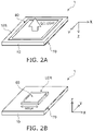
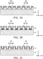
- FIGS. 2A and 2B are perspective views schematically showing the semiconductor light-emitting device 1 according to the embodiment.
- FIG. 2A is a schematic view showing the backside of the semiconductor device 1.
- FIG. 2B is a schematic view showing the front side of the semiconductor device 1.
- the QCL light is radiated from the back surface 10B of the semiconductor substrate 10.
- the back electrode 80 surrounds the region where the QCL light is radiated.
- a mesa-shaped light-emitting region LER is provided at the front side of the semiconductor substrate 10.
- the insulating film 70 covers the side surface of the light-emitting region LER and the front side of the semiconductor substrate 10.
- the light-emitting region LER includes the first semiconductor layer 20, the light-emitting layer 30, the second semiconductor layer 40, and the third semiconductor layer 50.
- the front electrode 60 covers the PC 50f at the upper surface of the light-emitting region LER.
- the upper surface of the light-emitting region LER has a square shape of which the length of one side is 500 ⁇ m.
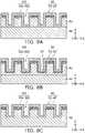
- FIGS. 3A to 3C are schematic cross-sectional views illustrating the structures of the PC 50f in the semiconductor light-emitting device 1 according to the embodiment.
- the PC 50f may have one of the structures shown in FIGS. 3A to 3C .
- the PC 50f is provided at the upper side of the third semiconductor layer 50 opposite to the second semiconductor layer 40.
- the PC 50f includes a protrusion 50a and a recess 50b. Multiple protrusions 50a are provided; and the recess 50b is provided between adjacent protrusions 50a.
- the multiple protrusions 50a are arranged in a direction, e.g., an X-direction, that is along the upper surface of the second semiconductor layer 40.
- the protrusions 50a are arranged in the X-direction at a constant period.
- the protrusions 50a also are arranged at a constant period in a Y-direction (not-illustrated). For example, the period of the protrusions 50a is less than the wavelength of the QCL light in each of the X-direction and the Y-direction.
- the front electrode 60 includes a first metal layer 63 and a second metal layer 65 and covers the PC 50f.
- the first metal layer 63 is, for example, a gold (Au) layer.
- the second metal layer 65 is, for example, a titanium (Ti) layer.
- the second metal layer 65 may be a nickel (Ni) layer or a chrome (Cr) layer.
- the second metal layer 65 is provided between the third semiconductor layer 50 and the first metal layer 63.
- the adhesion strength of the second metal layer 65 to the third semiconductor layer 50 is greater than the adhesion strength of the first metal layer 63 to the third semiconductor layer 50.
- the adhesion strength of the second metal layer 65 to the uneven structure that includes the protrusion 50a and the recess 50b is greater than the adhesion strength of the first metal layer 63 to the uneven structure.
- the adhesion strength of the second metal layer 65 to the uneven structure decreases when the layer thickness of the second metal layer 65 is thin.
- the adhesion strength of the second metal layer 65 to the uneven structure becomes insufficient when the layer thickness of the Ti layer is not more than 25 nanometers (nm).
- the reflectance of the first metal layer 63 for the QCL light radiated by the light-emitting layer 30 is greater than the reflectance of the second metal layer 65 for the QCL light.
- the absorptance of the second metal layer 65 for the QCL light is greater than the absorptance of the first metal layer 63 for the QCL light.
- the reflectance for the QCL light of the electrode in which the Ti layer and the Au layer (the first metal layer 63) are stacked is 40% less than the reflectance for the QCL light of an electrode of the Au layer without the Ti layer interposed.
- the second metal layer 65 is provided at the upper surface of the protrusion 50a but is not provided on the side surface of the protrusion 50a and on the bottom surface of the recess 50b.
- the layer thickness of the second metal layer 65 is, for example, 50 nm.
- the first metal layer 63 contacts the side surface of the protrusion 50a and the bottom surface of the recess 50b.
- the reflectance of the front electrode 60 shown in FIG. 3A is, for example, about 20% greater than a reflectance in the case where the layer thickness of the second metal layer 65 is 50 nm and the second metal layer 65 covers the entire surface of the uneven structure.
- the second metal layer 65 is provided on the bottom surface of the recess 50b but is not provided on the upper surface and the side surface of the protrusion 50a.
- the layer thickness of the second metal layer 65 is, for example, 50 nm.
- the first metal layer 63 contacts the upper surface and the side surface of the protrusion 50a.
- the reflectance of the front electrode 60 can be about 20% greater than the reflectance in the case where the second metal layer 65 covers the entire surface of the uneven structure.
- the second metal layer 65 is provided on the side surface of the protrusion 50a but is not provided on the upper surface of the protrusion 50a and the bottom surface of the recess 50b.
- the layer thickness of the second metal layer 65 is, for example, 50 nm.
- the first metal layer 63 contacts the upper surface of the protrusion 50a and the bottom surface of the recess 50b.
- the reflectance of the front electrode 60 can be greater than the reflectance in the case where the second metal layer 65 covers the entire surface of the uneven structure.
- the effective refractive index difference between the recess 50b and the protrusion 50a of the PC 50f can be increased by partially providing the second metal layer 65.
- the function of the PC 50f can be improved thereby.
- FIGS. 4A and 4B are schematic cross-sectional views showing a method for manufacturing the PC 50f according to the embodiment.
- multiple second metal layers 65 are formed on the third semiconductor layer 50.
- the second metal layers 65 are arranged at a constant periodicity in each of the X-direction and the Y-direction along the upper surface of the third semiconductor layer 50.
- the protrusion 50a and the recess 50b are formed by selectively removing the third semiconductor layer 50.
- the second metal layer 65 can be used as an etching mask.
- the first metal layer 63 is formed to cover the second metal layers 65 and the inner surfaces of the recesses 50b.
- the PC 50f and the front electrode 60 can be formed thereby.
- FIGS. 5A to 5C are schematic cross-sectional views showing a method for manufacturing the PC 50f according to a first modification of the embodiment.
- the protrusion 50a and the recess 50b are formed by selectively removing the third semiconductor layer 50 after forming an etching mask 53 on the third semiconductor layer 50.
- the etching mask 53 is, for example, a photoresist.
- the second metal layer 65 is formed on the third semiconductor layer 50.
- the second metal layer 65 is formed using, for example, a deposition method such as vacuum vapor deposition that has high directivity. Thereby, the second metal layer 65 is formed on the etching mask 53 and on the bottom surface of the recess 50b. In this process, the deposition of the second metal layer 65 is suppressed on the side surface of the protrusion 50a.
- the second metal layer 65 that is formed on the etching mask 53 is removed together with the etching mask 53. Thereby, the second metal layer 65 remains on the bottom surface of the recess 50b; and the upper surface and the side surface of the protrusion 50a are exposed.
- the first metal layer 63 is formed to cover the protrusion 50a and the bottom surface of the recess 50b.
- the PC 50f and the front electrode 60 can be formed thereby as shown in FIG. 3B .
- FIGS. 6A and 6B are schematic cross-sectional views showing a method for manufacturing the PC 50f according to a second modification of the embodiment.
- the second metal layer 65 is formed to cover the protrusion 50a and the recess 50b.
- the second metal layer 65 is formed so that the a space remains in the recess 50b.
- the protrusion 50a and the recess 50b are formed by selectively removing the third semiconductor layer 50.
- the third semiconductor layer 50 is removed using the etching mask 53 (referring to FIG. 5A ).
- the second metal layer 65 is formed after removing the etching mask 53.
- the second metal layer 65 is formed using a deposition method such as sputtering and like that has good step coverage.
- the second metal layer 65 is removed so that the portion formed on the side surface of the protrusion 50a remains.
- the second metal layer 65 is removed using, for example, anisotropic RIE (Reactive Ion Etching).
- the first metal layer 63 is formed to cover the protrusion 50a and the bottom surface of the recess 50b.
- the PC 50f and the front electrode 60 can be formed thereby.
- FIGS. 7A to 7D are schematic cross-sectional views showing a method for manufacturing the PC 50f according to a third modification of the embodiment.
- an insulating film 55 is formed to cover the protrusion 50a and the recess 50b.
- the insulating film 55 is formed so that a space remains in the recess 50b.
- the insulating film 55 is, for example, a silicon oxide film.
- a sacrificial film 57 is formed on the insulating film 55.
- the sacrificial film 57 fills the recess 50b.
- the sacrificial film 57 is, for example, a silicon nitride film.
- the insulating film 55 and the sacrificial film 57 are removed so that the portion formed in the recess 50b remains; and the upper surface of the protrusion 50a is exposed.
- the second metal layer 65 is formed after removing the sacrificial film 57.
- the second metal layer 65 is formed using, for example, a deposition method such as vacuum vapor deposition that has high directivity.
- the second metal layer 65 is formed on the upper surface of the protrusion 50a and the bottom surface of the recess 50b.
- the second metal layer 65 is formed on the bottom surface of the recess 50b with the insulating film 55 interposed.
- the portion of the second metal layer 65 that is formed on the bottom surface of the recess 50b is removed together with the insulating film 55.
- the insulating film 55 is removed using, for example, wet etching.
- the first metal layer 63 is formed to cover the protrusion 50a and the bottom surface of the recess 50b.
- the PC 50f and the front electrode 60 can be formed thereby.
- FIGS. 8A to 8C are schematic cross-sectional views showing the PC 50f according to modifications of the embodiment.
- the PC 50f is formed by removing the third semiconductor layer 50 so that the second semiconductor layer 40 is exposed at the bottom surface of the recess 50b.
- the second metal layer 65 is provided at the upper surface of the protrusion 50a.
- the first metal layer 63 is provided to cover the protrusion 50a and the recess 50b. The first metal layer 63 contacts the second semiconductor layer 40 exposed at the bottom surface of the recess 50b.
- the second metal layer 65 is provided at the upper surface of the protrusion 50a of the PC 50f.
- a third metal layer 67 is provided on the side surface of the protrusion 50a and on the bottom surface of the recess 50b.
- the third metal layer 67 is provided between the first metal layer 63 and the third semiconductor layer 50.
- the layer thickness of the third metal layer 67 is less than the layer thickness of the second metal layer 65.
- the third metal layer 67 includes, for example, the same material as the second metal layer 65.
- the reflectance of the front electrode 60 can be increased by providing the third metal layer 67 with the layer thickness less than the layer thickness of the second metal layer 65.
- a prescribed adhesion strength between the PC 50f and the front electrode 60 can be ensured by providing the second metal layer 65.
- the partial reduction of the adhesion strength at the side surface of the protrusion 50a and the bottom surface of the recess 50b can be mitigated by providing the third metal layer 67 between the first metal layer 63 and the third semiconductor layer 50.
- the third semiconductor layer 50 is not provided, and the PC 50f is provided at the upper surface of the second semiconductor layer 40 at the side opposite to the light-emitting layer 30.
- the third metal layer 67 shown in FIG. 8B is applicable to the examples shown in FIGS. 8A and 8C .
- the second metal layer 65 is provided at the upper surface of the protrusion 50a, the embodiments are not limited thereto. In other words, the features shown in FIGS. 8A to 8C are applicable even when the second metal layer 65 is provided on the bottom surface of the recess 50b or on the side surface of the protrusion 50a.
- FIGS. 9A and 9B are schematic cross-sectional views showing surface light-emission type semiconductor light-emitting devices 2 and 3 according to modifications of the embodiment.
- the light-emitting region LER has the mesa structure; and the front electrode 60 covers the side surface of the light-emitting region LER with the insulating film 70 interposed. Thereby, the light that is radiated toward the outside from the side surface of the light-emitting region LER is returned to the interior of the light-emitting region LER; and the intensity of the QCL light can be increased.
- the light-emitting region LER has the mesa structure; and the front electrode 60 covers the side surface of the light-emitting region LER with the insulating film 70 interposed.
- the front electrode 60 includes the portion that is provided on the side surface of the light-emitting region LER without the second metal layer 65 interposed; and the first metal layer 63 directly contacts the insulating film 70.
- the reflectance at the portion of the front electrode 60 that is provided on the side surface of the light-emitting region LER can be improved thereby; and the intensity of the QCL light can be further increased.
Landscapes
- Physics & Mathematics (AREA)
- Condensed Matter Physics & Semiconductors (AREA)
- General Physics & Mathematics (AREA)
- Electromagnetism (AREA)
- Optics & Photonics (AREA)
- Led Devices (AREA)
- Semiconductor Lasers (AREA)
Abstract
Description
- Embodiments relate to a surface light-emission type semiconductor light-emitting device.
- The surface light-emission type semiconductor light-emitting device is required to have a large light output.
-
-
FIG. 1 is a schematic cross-sectional view showing a surface light emission type semiconductor light-emitting device according to an embodiment; -
FIGS. 2A and 2B are perspective views schematically showing the surface light emission type semiconductor light-emitting device according to the embodiment; -
FIGS. 3A to 3C are schematic cross-sectional views illustrating the structures of photonic crystals of the surface light-emission type semiconductor light-emitting device according to the embodiment; -
FIGS. 4A and 4B are schematic cross-sectional views showing a method for manufacturing a photonic crystal according to the embodiment; -
FIGS. 5A to 5C are schematic cross-sectional views showing a method for manufacturing a photonic crystal according to a first modification of the embodiment; -
FIGS. 6A and 6B are schematic cross-sectional views showing a method for manufacturing a photonic crystal according to a second modification of the embodiment; -
FIGS. 7A to 7D are schematic cross-sectional views showing a method for manufacturing a photonic crystal according to a third modification of the embodiment; -
FIGS. 8A to 8C are schematic cross-sectional views showing photonic crystals according to modifications of the embodiment; and -
FIGS. 9A and 9B are schematic cross-sectional views showing surface light-emission type semiconductor light-emitting devices according to modifications of the embodiment. - According to an embodiment, a surface light-emission type semiconductor light-emitting device includes a first semiconductor layer; a light-emitting layer provided on the first semiconductor layer; a second semiconductor layer provided on the light-emitting layer; an uneven structure provided on the second semiconductor layer, the uneven structure including a protrusion and a recess next to the protrusion; a first metal layer covering the uneven structure; and a second metal layer provided between the uneven structure and the first metal layer. The second metal layer is provided on one of a bottom surface of the recess, an upper surface of the protrusion, or a side surface of the protrusion. The second metal layer has a reflectance for light radiated from the light-emitting layer, which is less than a reflectance of the first metal layer for the light.
- Embodiments will now be described with reference to the drawings. The same portions inside the drawings are marked with the same numerals; a detailed description is omitted as appropriate; and the different portions are described. The drawings are schematic or conceptual; and the relationships between the thicknesses and widths of portions, the proportions of sizes between portions, etc., are not necessarily the same as the actual values thereof. The dimensions and/or the proportions may be illustrated differently between the drawings, even in the case where the same portion is illustrated.
- There are cases where the dispositions of the components are described using the directions of XYZ axes shown in the drawings. The X-axis, the Y-axis, and the Z-axis are orthogonal to each other. Hereinbelow, the directions of the X-axis, the Y-axis, and the Z-axis are described as an X-direction, a Y-direction, and a Z-direction. Also, there are cases where the Z-direction is described as upward and the direction opposite to the Z-direction is described as downward.
-
FIG. 1 is a schematic cross-sectional view showing a surface light-emission type semiconductor light-emitting device 1 according to an embodiment. The semiconductor light-emitting device 1 is, for example, a surface light-emitting QCL (Quantum Cascade Laser). - The semiconductor light-
emitting device 1 includes asemiconductor substrate 10, afirst semiconductor layer 20, a light-emitting layer 30, asecond semiconductor layer 40, athird semiconductor layer 50, afront electrode 60, aninsulating film 70, and aback electrode 80. - The
semiconductor substrate 10 is, for example, an n-type indium phosphide (InP) substrate. Thesemiconductor substrate 10 may be an n-type GaAs substrate. - The
first semiconductor layer 20 is provided on thesemiconductor substrate 10. Thefirst semiconductor layer 20 is, for example, an n-type InP layer. A buffer layer may be provided between thesemiconductor substrate 10 and thefirst semiconductor layer 20. - The light-emitting
layer 30 is provided on thefirst semiconductor layer 20. For example, the light-emittinglayer 30 includes a quantum well structure that generates intersubband transitions of carriers. The light-emittinglayer 30 includes, for example, an n-type Group III-V compound semiconductor doped with silicon, and emits light due to subband transitions of electrons. - The light-emitting
layer 30 includes, for example, a quantum well structure in which aquantum well layer 33 and abarrier layer 35 are alternately stacked in a direction, e.g., a Z-direction, that is orthogonal to the upper surface of thefirst semiconductor layer 20. Thequantum well layer 33 includes, for example, a first compound semiconductor (InGaAs); and thebarrier layer 35 includes, for example, a second compound semiconductor (AlInAs). - Here, InGaAs is a compound semiconductor of the compositional formula In x Ga1-x As (0 < x < 1). AlInAs is another compound semiconductor of the compositional formula Al y In1-y As (0 < y < 1).
- The light-emitting
layer 30 includes, for example, a light-emitting multi-quantum well region that includes the first and second compound semiconductors, and an injection multi-quantum well region that includes other first and second compound semiconductors. The light-emittinglayer 30 includes multiple pairs of the light-emitting multi-quantum well region and the injection multi-quantum well region that are stacked alternately. - The
second semiconductor layer 40 is provided on the light-emittinglayer 30. Thesecond semiconductor layer 40 is, for example, an n-type InP layer. - The
third semiconductor layer 50 is provided on thesecond semiconductor layer 40. Thethird semiconductor layer 50 is, for example, an n-type InGaAs layer. A photonic crystal (PC) is provided in thethird semiconductor layer 50. The photonic crystal (hereinbelow, thePC 50f) includes an uneven structure that has a constant periodicity. The PC 50f acts as a waveguide which guides the light radiated from the light-emittinglayer 30 in a direction perpendicular to the upper surface of thesemiconductor substrate 10. - The
PC 50f functions as a photonic crystal that selects the wavelength and controls the emission angle of the laser light. The PC50f is designed so that the light having desired wavelength resonates inside the light-emittinglayer 30 and induces laser oscillation. The laser light is emitted in a direction that is substantially perpendicular to the boundary between the light-emittinglayer 30 and thefirst semiconductor layer 20. Here, "substantially perpendicular" means that the angle with respect to the boundary between the light-emittinglayer 30 and thefirst semiconductor layer 20 is not less than 81° and not more than 99°. The PC 50f includes multiple recesses that are, for example, periodically arranged as a two-dimensional diffraction grating. For example, the recesses of the PC 50f are right-triangular in the top-view of thethird semiconductor layer 50. The shapes of the recesses and the arrangement of the protrusions are not limited to those of the examples. - The
front electrode 60 is provided on thethird semiconductor layer 50. Thefront electrode 60 covers thePC 50f. Thefront electrode 60 reflects the light radiated from the light-emittinglayer 30. - The semiconductor light-emitting
device 1 has a mesa structure that includes thefirst semiconductor layer 20, the light-emittinglayer 30, thesecond semiconductor layer 40, and thethird semiconductor layer 50. The insulatingfilm 70 covers the side surface of the mesa structure. The insulatingfilm 70 is, for example, a silicon oxide film. The insulatingfilm 70 also covers the surface of thesemiconductor substrate 10 with a portion of thefirst semiconductor layer 20 interposed. - The
back electrode 80 is provided on aback surface 10B of thesemiconductor substrate 10. Theback electrode 80 includes, for example, a titanium (Ti)layer 81 and a gold (Au)layer 83. TheTi layer 81 is provided between thesemiconductor substrate 10 and theAu layer 83. - In the semiconductor light-emitting
device 1, a driving current flows between thefront electrode 60 and theback electrode 80, and the carriers (the electrons) are injected into the light-emittinglayer 30. The light-emittinglayer 30 emits QCL light guided by thePC 50f. The QCL light is generated by stimulated emission due to the energy relaxation of the carriers in thequantum well layer 33. The QCL light is radiated externally from theback surface 10B of thesemiconductor substrate 10. The wavelength of the QCL light is, for example, 4.5 micrometers (µm). -
FIGS. 2A and 2B are perspective views schematically showing the semiconductor light-emittingdevice 1 according to the embodiment.FIG. 2A is a schematic view showing the backside of thesemiconductor device 1.FIG. 2B is a schematic view showing the front side of thesemiconductor device 1. - As shown in
FIG. 2A , the QCL light is radiated from theback surface 10B of thesemiconductor substrate 10. Theback electrode 80 surrounds the region where the QCL light is radiated. - As shown in
FIG. 2B , a mesa-shaped light-emitting region LER is provided at the front side of thesemiconductor substrate 10. The insulatingfilm 70 covers the side surface of the light-emitting region LER and the front side of thesemiconductor substrate 10. - The light-emitting region LER includes the
first semiconductor layer 20, the light-emittinglayer 30, thesecond semiconductor layer 40, and thethird semiconductor layer 50. Thefront electrode 60 covers thePC 50f at the upper surface of the light-emitting region LER. For example, the upper surface of the light-emitting region LER has a square shape of which the length of one side is 500 µm. -
FIGS. 3A to 3C are schematic cross-sectional views illustrating the structures of thePC 50f in the semiconductor light-emittingdevice 1 according to the embodiment. ThePC 50f may have one of the structures shown inFIGS. 3A to 3C . - The
PC 50f is provided at the upper side of thethird semiconductor layer 50 opposite to thesecond semiconductor layer 40. ThePC 50f includes aprotrusion 50a and arecess 50b.Multiple protrusions 50a are provided; and therecess 50b is provided betweenadjacent protrusions 50a. Themultiple protrusions 50a are arranged in a direction, e.g., an X-direction, that is along the upper surface of thesecond semiconductor layer 40. Theprotrusions 50a are arranged in the X-direction at a constant period. Theprotrusions 50a also are arranged at a constant period in a Y-direction (not-illustrated). For example, the period of theprotrusions 50a is less than the wavelength of the QCL light in each of the X-direction and the Y-direction. - The
front electrode 60 includes afirst metal layer 63 and asecond metal layer 65 and covers thePC 50f. Thefirst metal layer 63 is, for example, a gold (Au) layer. Thesecond metal layer 65 is, for example, a titanium (Ti) layer. Alternatively, thesecond metal layer 65 may be a nickel (Ni) layer or a chrome (Cr) layer. - The
second metal layer 65 is provided between thethird semiconductor layer 50 and thefirst metal layer 63. The adhesion strength of thesecond metal layer 65 to thethird semiconductor layer 50 is greater than the adhesion strength of thefirst metal layer 63 to thethird semiconductor layer 50. In other words, the adhesion strength of thesecond metal layer 65 to the uneven structure that includes theprotrusion 50a and therecess 50b is greater than the adhesion strength of thefirst metal layer 63 to the uneven structure. - The adhesion strength of the
second metal layer 65 to the uneven structure decreases when the layer thickness of thesecond metal layer 65 is thin. For example, the adhesion strength of thesecond metal layer 65 to the uneven structure becomes insufficient when the layer thickness of the Ti layer is not more than 25 nanometers (nm). - On the other hand, the reflectance of the
first metal layer 63 for the QCL light radiated by the light-emittinglayer 30 is greater than the reflectance of thesecond metal layer 65 for the QCL light. In other words, the absorptance of thesecond metal layer 65 for the QCL light is greater than the absorptance of thefirst metal layer 63 for the QCL light. - For example, when the layer thickness of the Ti layer (the second metal layer 65) is 50 nm, the reflectance for the QCL light of the electrode in which the Ti layer and the Au layer (the first metal layer 63) are stacked is 40% less than the reflectance for the QCL light of an electrode of the Au layer without the Ti layer interposed.
- In the example shown in
FIG. 3A , thesecond metal layer 65 is provided at the upper surface of theprotrusion 50a but is not provided on the side surface of theprotrusion 50a and on the bottom surface of therecess 50b. The layer thickness of thesecond metal layer 65 is, for example, 50 nm. Thefirst metal layer 63 contacts the side surface of theprotrusion 50a and the bottom surface of therecess 50b. The reflectance of thefront electrode 60 shown inFIG. 3A is, for example, about 20% greater than a reflectance in the case where the layer thickness of thesecond metal layer 65 is 50 nm and thesecond metal layer 65 covers the entire surface of the uneven structure. - In the example shown in
FIG. 3B , thesecond metal layer 65 is provided on the bottom surface of therecess 50b but is not provided on the upper surface and the side surface of theprotrusion 50a. The layer thickness of thesecond metal layer 65 is, for example, 50 nm. Thefirst metal layer 63 contacts the upper surface and the side surface of theprotrusion 50a. Also, in the example, the reflectance of thefront electrode 60 can be about 20% greater than the reflectance in the case where thesecond metal layer 65 covers the entire surface of the uneven structure. - In the example shown in
FIG. 3C , thesecond metal layer 65 is provided on the side surface of theprotrusion 50a but is not provided on the upper surface of theprotrusion 50a and the bottom surface of therecess 50b. The layer thickness of thesecond metal layer 65 is, for example, 50 nm. Thefirst metal layer 63 contacts the upper surface of theprotrusion 50a and the bottom surface of therecess 50b. Also, in the example, the reflectance of thefront electrode 60 can be greater than the reflectance in the case where thesecond metal layer 65 covers the entire surface of the uneven structure. - In the examples shown in
FIGS. 3A and 3C , the effective refractive index difference between therecess 50b and theprotrusion 50a of thePC 50f can be increased by partially providing thesecond metal layer 65. The function of thePC 50f can be improved thereby. -
FIGS. 4A and 4B are schematic cross-sectional views showing a method for manufacturing thePC 50f according to the embodiment. - As shown in
FIG. 4A , multiple second metal layers 65 are formed on thethird semiconductor layer 50. For example, the second metal layers 65 are arranged at a constant periodicity in each of the X-direction and the Y-direction along the upper surface of thethird semiconductor layer 50. - As shown in
FIG. 4B , theprotrusion 50a and therecess 50b are formed by selectively removing thethird semiconductor layer 50. Thesecond metal layer 65 can be used as an etching mask. Subsequently, thefirst metal layer 63 is formed to cover the second metal layers 65 and the inner surfaces of therecesses 50b. As shown inFIG. 3A , thePC 50f and thefront electrode 60 can be formed thereby. -
FIGS. 5A to 5C are schematic cross-sectional views showing a method for manufacturing thePC 50f according to a first modification of the embodiment. - As shown in
FIG. 5A , theprotrusion 50a and therecess 50b are formed by selectively removing thethird semiconductor layer 50 after forming anetching mask 53 on thethird semiconductor layer 50. Theetching mask 53 is, for example, a photoresist. - As shown in
FIG. 5B , thesecond metal layer 65 is formed on thethird semiconductor layer 50. Thesecond metal layer 65 is formed using, for example, a deposition method such as vacuum vapor deposition that has high directivity. Thereby, thesecond metal layer 65 is formed on theetching mask 53 and on the bottom surface of therecess 50b. In this process, the deposition of thesecond metal layer 65 is suppressed on the side surface of theprotrusion 50a. - As shown in
FIG. 5C , thesecond metal layer 65 that is formed on theetching mask 53 is removed together with theetching mask 53. Thereby, thesecond metal layer 65 remains on the bottom surface of therecess 50b; and the upper surface and the side surface of theprotrusion 50a are exposed. - Then, the
first metal layer 63 is formed to cover theprotrusion 50a and the bottom surface of therecess 50b. ThePC 50f and thefront electrode 60 can be formed thereby as shown inFIG. 3B . -
FIGS. 6A and 6B are schematic cross-sectional views showing a method for manufacturing thePC 50f according to a second modification of the embodiment. - As shown in
FIG. 6A , thesecond metal layer 65 is formed to cover theprotrusion 50a and therecess 50b. Thesecond metal layer 65 is formed so that the a space remains in therecess 50b. - For example, the
protrusion 50a and therecess 50b are formed by selectively removing thethird semiconductor layer 50. Thethird semiconductor layer 50 is removed using the etching mask 53 (referring toFIG. 5A ). Thesecond metal layer 65 is formed after removing theetching mask 53. Thesecond metal layer 65 is formed using a deposition method such as sputtering and like that has good step coverage. - As shown in
FIG. 6B , thesecond metal layer 65 is removed so that the portion formed on the side surface of theprotrusion 50a remains. Thesecond metal layer 65 is removed using, for example, anisotropic RIE (Reactive Ion Etching). Then, thefirst metal layer 63 is formed to cover theprotrusion 50a and the bottom surface of therecess 50b. As shown inFIG. 3C , thePC 50f and thefront electrode 60 can be formed thereby. -
FIGS. 7A to 7D are schematic cross-sectional views showing a method for manufacturing thePC 50f according to a third modification of the embodiment. - As shown in
FIG. 7A , an insulatingfilm 55 is formed to cover theprotrusion 50a and therecess 50b. The insulatingfilm 55 is formed so that a space remains in therecess 50b. The insulatingfilm 55 is, for example, a silicon oxide film. Then, asacrificial film 57 is formed on the insulatingfilm 55. Thesacrificial film 57 fills therecess 50b. Thesacrificial film 57 is, for example, a silicon nitride film. - As shown in
FIG. 7B , the insulatingfilm 55 and thesacrificial film 57 are removed so that the portion formed in therecess 50b remains; and the upper surface of theprotrusion 50a is exposed. - As shown in
FIG. 7C , thesecond metal layer 65 is formed after removing thesacrificial film 57. Thesecond metal layer 65 is formed using, for example, a deposition method such as vacuum vapor deposition that has high directivity. Thesecond metal layer 65 is formed on the upper surface of theprotrusion 50a and the bottom surface of therecess 50b. Thesecond metal layer 65 is formed on the bottom surface of therecess 50b with the insulatingfilm 55 interposed. - As shown in
FIG. 7D , the portion of thesecond metal layer 65 that is formed on the bottom surface of therecess 50b is removed together with the insulatingfilm 55. The insulatingfilm 55 is removed using, for example, wet etching. Subsequently, thefirst metal layer 63 is formed to cover theprotrusion 50a and the bottom surface of therecess 50b. As shown inFIG. 3A , thePC 50f and thefront electrode 60 can be formed thereby. -
FIGS. 8A to 8C are schematic cross-sectional views showing thePC 50f according to modifications of the embodiment. - In the example shown in
FIG. 8A , thePC 50f is formed by removing thethird semiconductor layer 50 so that thesecond semiconductor layer 40 is exposed at the bottom surface of therecess 50b. Thesecond metal layer 65 is provided at the upper surface of theprotrusion 50a. Thefirst metal layer 63 is provided to cover theprotrusion 50a and therecess 50b. Thefirst metal layer 63 contacts thesecond semiconductor layer 40 exposed at the bottom surface of therecess 50b. - In the example shown in
FIG. 8B , thesecond metal layer 65 is provided at the upper surface of theprotrusion 50a of thePC 50f. Athird metal layer 67 is provided on the side surface of theprotrusion 50a and on the bottom surface of therecess 50b. Thethird metal layer 67 is provided between thefirst metal layer 63 and thethird semiconductor layer 50. The layer thickness of thethird metal layer 67 is less than the layer thickness of thesecond metal layer 65. Thethird metal layer 67 includes, for example, the same material as thesecond metal layer 65. - In the example as well, the reflectance of the
front electrode 60 can be increased by providing thethird metal layer 67 with the layer thickness less than the layer thickness of thesecond metal layer 65. In thePC 50f according to the embodiment, a prescribed adhesion strength between thePC 50f and thefront electrode 60 can be ensured by providing thesecond metal layer 65. However, when thefirst metal layer 63 directly contacts thethird semiconductor layer 50, a partial reduction of the adhesion strength cannot be avoided. In the example, the partial reduction of the adhesion strength at the side surface of theprotrusion 50a and the bottom surface of therecess 50b can be mitigated by providing thethird metal layer 67 between thefirst metal layer 63 and thethird semiconductor layer 50. - In the example shown in
FIG. 8C , thethird semiconductor layer 50 is not provided, and thePC 50f is provided at the upper surface of thesecond semiconductor layer 40 at the side opposite to the light-emittinglayer 30. - The
third metal layer 67 shown inFIG. 8B is applicable to the examples shown inFIGS. 8A and 8C . Although, in the examples of thePC 50f shown inFIGS. 8A to 8C , thesecond metal layer 65 is provided at the upper surface of theprotrusion 50a, the embodiments are not limited thereto. In other words, the features shown inFIGS. 8A to 8C are applicable even when thesecond metal layer 65 is provided on the bottom surface of therecess 50b or on the side surface of theprotrusion 50a. -
FIGS. 9A and 9B are schematic cross-sectional views showing surface light-emission type semiconductor light-emittingdevices - In the semiconductor light-emitting
device 2 shown inFIG. 9A , the light-emitting region LER has the mesa structure; and thefront electrode 60 covers the side surface of the light-emitting region LER with the insulatingfilm 70 interposed. Thereby, the light that is radiated toward the outside from the side surface of the light-emitting region LER is returned to the interior of the light-emitting region LER; and the intensity of the QCL light can be increased. - Also, in the semiconductor light-emitting
device 3 shown inFIG. 9B , the light-emitting region LER has the mesa structure; and thefront electrode 60 covers the side surface of the light-emitting region LER with the insulatingfilm 70 interposed. In the example, thefront electrode 60 includes the portion that is provided on the side surface of the light-emitting region LER without thesecond metal layer 65 interposed; and thefirst metal layer 63 directly contacts the insulatingfilm 70. The reflectance at the portion of thefront electrode 60 that is provided on the side surface of the light-emitting region LER can be improved thereby; and the intensity of the QCL light can be further increased. - While certain embodiments have been described, these embodiments have been presented by way of example only, and are not intended to limit the scope of the inventions. Indeed, the novel embodiments described herein may be embodied in a variety of other forms; furthermore, various omissions, substitutions and changes in the form of the embodiments described herein may be made without departing from the spirit of the inventions. The accompanying claims and their equivalents are intended to cover such forms or modifications as would fall within the scope and spirit of the invention.
Claims (15)
- A surface light-emission type semiconductor light-emitting device (1, 2, 3), the device comprising:a first semiconductor layer (20);a light-emitting layer (30) provided on the first semiconductor layer (20);a second semiconductor layer (40) provided on the light-emitting layer (30);an uneven structure (50f) provided on the second semiconductor layer (40), the uneven structure (50f) including a protrusion (50a) and a recess (50b) next to the protrusion (50a);a first metal layer (63) covering the uneven structure (50f); anda second metal layer (65) provided between the uneven structure (50f) and the first metal layer (63), the second metal layer (65) being provided on one of a bottom surface of the recess (50b), an upper surface of the protrusion (50a), or a side surface of the protrusion (50a),a reflectance of the second metal layer (65) for light radiated from the light-emitting layer (30) being less than a reflectance of the first metal layer (63) for the light.
- The device (1, 2, 3) according to claim 1, wherein
the second metal layer (65) has an adhesion strength to the uneven structure (50f), the adhesion strength of the second metal layer (65) being greater than an adhesion strength of the first metal layer (63) to the uneven structure (50f). - The device (1, 2, 3) according to claim 1 or 2, wherein the first semiconductor layer (20) and the second semiconductor layer (40) are of a same conductivity type.
- The device (1, 2, 3) according to any one of claims 1 to 3, wherein the first metal layer (63) includes gold, and the second metal layer (65) includes titanium.
- The device (1, 2, 3) according to any one of claims 1 to 4, wherein the first metal layer (63) contacts the surfaces other than the one of the bottom surface of the recess (50b), the upper surface of the protrusion (50a), or the side surface of the protrusion (50a).
- The device (1, 2, 3) according to any one of claims 1 to 4, further comprising:a third metal layer (67) provided between the uneven structure (50f) and the first metal layer (63),the third metal layer (67) provided on the surfaces other than the one of the bottom surface of the recess (50b), the upper surface of the protrusion (50a), or the side surface of the protrusion (50a),the third metal layer (67) having a layer thickness thinner than a layer thickness of the second metal layer (65).
- The device (1, 2, 3) according to claim 6, wherein
the third metal layer (67) has an adhesion strength to the uneven structure (50f), the adhesion strength of the third metal layer (67) being greater than an adhesion strength of the first metal layer (63) to the uneven structure (50f). - The device (1, 2, 3) according to claim 6 or 7, wherein the third metal layer (67) includes a metal material same as a metal material of the second metal layer (65).
- The device (1, 2, 3) according to any one of claims 1 to 8, further comprising:
a third semiconductor layer (50) provided on the second semiconductor layer (40), the uneven structure (50f) being provided in the third semiconductor layer (50). - The device (1, 2, 3) according to claim 9, whereinthe first semiconductor layer (20) and the second semiconductor layer (40) each include indium phosphide, andthe third semiconductor layer (50) includes an indium gallium arsenide mixed crystal.
- The device (1, 2, 3) according to claim 9 or 10, wherein the second semiconductor layer (40) is exposed at the bottom surface of the recess (50b) of the uneven structure (50f).
- The device (1, 2, 3) according to claim 9 or 10, wherein the third semiconductor layer (50) is exposed at the bottom surface of the recess (50b) and the side surface of the protrusion (50a) in the uneven structure (50f).
- The device (1, 2, 3) according to any one of claims 1 to 12, whereinthe uneven structure (50f) includes a plurality of the protrusions (50a), andthe plurality of protrusions (50a) are arranged at a constant periodicity in a direction along an upper surface of the second semiconductor layer (40) so that a photonic crystal structure is configured by the plurality of protrusions (50a).
- The device (1, 2, 3) according to claim 13, wherein
the plurality of protrusions (50a) is arranged with a period less than a wavelength of the light radiated from the light-emitting layer (30). - The device (1, 2, 3) according to any one of claims 1 to 14, whereinthe light-emitting layer (30) includes first and second layers (33, 35) alternately stacked in a direction from the first semiconductor layer (20) toward the second semiconductor layer (40), the first layer (33) including a first compound semiconductor, the second layer (35) including a second compound semiconductor, the second compound semiconductor being different from the first compound semiconductor;the light-emitting layer (30) includes a light-emitting multi-quantum well region and an injection multi-quantum well region when operating as a quantum cascade laser, the light-emitting multi-quantum well region including the first and second compound semiconductors, the injection multi-quantum well region including other first and second compound semiconductors; andthe light-emitting layer (30) includes a structure in which a plurality of pairs of the light-emitting multi-quantum well region and the injection multi-quantum well region are stacked.
Applications Claiming Priority (1)
| Application Number | Priority Date | Filing Date | Title |
|---|---|---|---|
| JP2021026081A JP7662353B2 (en) | 2021-02-22 | 2021-02-22 | Surface-emitting semiconductor light-emitting device |
Publications (2)
| Publication Number | Publication Date |
|---|---|
| EP4047761A1 true EP4047761A1 (en) | 2022-08-24 |
| EP4047761B1 EP4047761B1 (en) | 2025-03-26 |
Family
ID=77627009
Family Applications (1)
| Application Number | Title | Priority Date | Filing Date |
|---|---|---|---|
| EP21194549.8A Active EP4047761B1 (en) | 2021-02-22 | 2021-09-02 | Surface light-emission type semiconductor light-emitting device |
Country Status (4)
| Country | Link |
|---|---|
| US (1) | US12506322B2 (en) |
| EP (1) | EP4047761B1 (en) |
| JP (1) | JP7662353B2 (en) |
| CN (1) | CN114976857B (en) |
Citations (5)
| Publication number | Priority date | Publication date | Assignee | Title |
|---|---|---|---|---|
| JP2009231773A (en) * | 2008-03-25 | 2009-10-08 | Sumitomo Electric Ind Ltd | Photonic crystal face emission laser element and method of manufacturing the same |
| EP2187456A2 (en) * | 2008-11-17 | 2010-05-19 | LG Innotek Co., Ltd. | Semiconductor light emitting device |
| EP2765618A2 (en) * | 2013-02-08 | 2014-08-13 | Kabushiki Kaisha Toshiba | Semiconductor light emitting device |
| US20190148915A1 (en) * | 2017-11-16 | 2019-05-16 | Kabushiki Kaisha Toshiba | Surface-emitting quantum cascade laser |
| JP2019197933A (en) * | 2019-08-23 | 2019-11-14 | 株式会社東芝 | Surface emission quantum cascade laser |
Family Cites Families (30)
| Publication number | Priority date | Publication date | Assignee | Title |
|---|---|---|---|---|
| WO1994013044A1 (en) * | 1992-12-03 | 1994-06-09 | Siemens Aktiengesellschaft | Tunable surface-emitting laser diode |
| JPH10178238A (en) * | 1996-12-18 | 1998-06-30 | Alps Electric Co Ltd | Manufacture of semiconductor laser |
| US6167072A (en) | 1997-06-06 | 2000-12-26 | University Of Florida | Modulated cap thin p-clad semiconductor laser |
| JP4292619B2 (en) | 1999-03-24 | 2009-07-08 | パナソニック株式会社 | Manufacturing method of semiconductor device |
| US6501783B1 (en) | 2000-02-24 | 2002-12-31 | Lucent Technologies Inc. | Distributed feedback surface plasmon laser |
| AUPS098002A0 (en) | 2002-03-08 | 2002-03-28 | University Of Western Australia, The | Tunable cavity resonator, and method of fabricating same |
| JP4130163B2 (en) | 2003-09-29 | 2008-08-06 | 三洋電機株式会社 | Semiconductor light emitting device |
| JP2006135311A (en) | 2004-10-08 | 2006-05-25 | Mitsubishi Cable Ind Ltd | Light-emitting diode using nitride semiconductor |
| KR100579320B1 (en) | 2004-11-15 | 2006-05-11 | 광주과학기술원 | Manufacturing method of nitride based light emitting device |
| EP2797185B1 (en) * | 2005-06-22 | 2018-09-05 | MACOM Technology Solutions Holdings, Inc. | AIGalnN-based lasers produced using etched facet technology |
| JP2007005591A (en) | 2005-06-24 | 2007-01-11 | Toshiba Corp | Semiconductor light emitting device |
| JP2007103690A (en) | 2005-10-05 | 2007-04-19 | Matsushita Electric Ind Co Ltd | Semiconductor light emitting device and manufacturing method thereof |
| JP5037835B2 (en) | 2006-02-28 | 2012-10-03 | キヤノン株式会社 | Vertical cavity surface emitting laser |
| US7701629B2 (en) | 2007-04-19 | 2010-04-20 | Hewlett-Packard Development Company, L.P. | Photonic device including semiconductor structure having doped region with array of subwavelengh recesses |
| FR2916092B1 (en) | 2007-05-11 | 2009-08-07 | Thales Sa | SEMICONDUCTOR LASER WITH STRONG REPEAT COUNTER-REACTION |
| JP2012059790A (en) * | 2010-09-06 | 2012-03-22 | Toshiba Corp | Semiconductor light-emitting element and manufacturing method of the same |
| JP2013021205A (en) * | 2011-07-13 | 2013-01-31 | Mitsubishi Electric Corp | Plane-emitting laser diode |
| CN103078050A (en) | 2013-02-01 | 2013-05-01 | 映瑞光电科技(上海)有限公司 | Flip LED (light-emitting diode) chip and manufacturing method thereof |
| CN103730556B (en) | 2013-12-31 | 2017-02-08 | 安徽三安光电有限公司 | Light-emitting diode chip and manufacturing method thereof |
| JP2017168591A (en) | 2016-03-15 | 2017-09-21 | 株式会社東芝 | Semiconductor laser device |
| JP6182230B1 (en) | 2016-03-15 | 2017-08-16 | 株式会社東芝 | Surface emitting quantum cascade laser |
| JP2018046128A (en) | 2016-09-14 | 2018-03-22 | 株式会社東芝 | Quantum cascade laser device |
| JP6557649B2 (en) | 2016-12-01 | 2019-08-07 | 株式会社東芝 | Quantum cascade laser |
| JP6801416B2 (en) | 2016-12-08 | 2020-12-16 | 住友電気工業株式会社 | Quantum cascade semiconductor laser |
| JP6747308B2 (en) | 2017-01-20 | 2020-08-26 | 豊田合成株式会社 | Light emitting element |
| JP6580097B2 (en) | 2017-09-05 | 2019-09-25 | 株式会社東芝 | Surface emitting quantum cascade laser |
| JP7093220B2 (en) | 2018-04-26 | 2022-06-29 | 浜松ホトニクス株式会社 | Quantum cascade laser |
| JP7125327B2 (en) | 2018-10-25 | 2022-08-24 | 浜松ホトニクス株式会社 | Light-emitting element and light-emitting device |
| JP2020092145A (en) | 2018-12-04 | 2020-06-11 | 株式会社東芝 | Quantum cascade laser and manufacturing method thereof |
| JP7129359B2 (en) | 2019-02-27 | 2022-09-01 | 株式会社東芝 | Semiconductor laser wafers and semiconductor lasers |
-
2021
- 2021-02-22 JP JP2021026081A patent/JP7662353B2/en active Active
- 2021-09-02 EP EP21194549.8A patent/EP4047761B1/en active Active
- 2021-09-02 US US17/464,765 patent/US12506322B2/en active Active
- 2021-09-07 CN CN202111042859.5A patent/CN114976857B/en active Active
Patent Citations (5)
| Publication number | Priority date | Publication date | Assignee | Title |
|---|---|---|---|---|
| JP2009231773A (en) * | 2008-03-25 | 2009-10-08 | Sumitomo Electric Ind Ltd | Photonic crystal face emission laser element and method of manufacturing the same |
| EP2187456A2 (en) * | 2008-11-17 | 2010-05-19 | LG Innotek Co., Ltd. | Semiconductor light emitting device |
| EP2765618A2 (en) * | 2013-02-08 | 2014-08-13 | Kabushiki Kaisha Toshiba | Semiconductor light emitting device |
| US20190148915A1 (en) * | 2017-11-16 | 2019-05-16 | Kabushiki Kaisha Toshiba | Surface-emitting quantum cascade laser |
| JP2019197933A (en) * | 2019-08-23 | 2019-11-14 | 株式会社東芝 | Surface emission quantum cascade laser |
Also Published As
| Publication number | Publication date |
|---|---|
| US20220271508A1 (en) | 2022-08-25 |
| JP7662353B2 (en) | 2025-04-15 |
| US12506322B2 (en) | 2025-12-23 |
| CN114976857A (en) | 2022-08-30 |
| JP2022127863A (en) | 2022-09-01 |
| EP4047761B1 (en) | 2025-03-26 |
| CN114976857B (en) | 2026-01-13 |
Similar Documents
| Publication | Publication Date | Title |
|---|---|---|
| CN110474230B (en) | Optoelectronic semiconductor component and method for producing an optoelectronic semiconductor component | |
| US7756177B2 (en) | Semiconductor light-emitting device | |
| US20080226223A1 (en) | Method of manufacturing a semiconductor device | |
| US8716044B2 (en) | Optical semiconductor device having ridge structure formed on active layer containing P-type region and its manufacture method | |
| US10404038B2 (en) | Quantum cascade laser | |
| JP2018098262A (en) | Quantum cascade laser diode | |
| EP1045457A2 (en) | Quantum well type light-emitting diode | |
| US10554022B2 (en) | Quantum cascade laser | |
| US9711944B2 (en) | Quantum cascade laser | |
| JP2021057517A (en) | Wavelength variable laser element and manufacturing method for the same | |
| JP4571635B2 (en) | Super luminescent diode | |
| US8536603B2 (en) | Optoelectronic semiconductor chip and method of producing an optoelectronic semiconductor chip | |
| EP4047761B1 (en) | Surface light-emission type semiconductor light-emitting device | |
| JP5273459B2 (en) | Manufacturing method of semiconductor laser | |
| US20240396306A1 (en) | Nitride semiconductor light-emitting element | |
| US7733935B2 (en) | Nitride semiconductor laser device and method of producing the same | |
| US20100238964A1 (en) | Semiconductor laser structure | |
| US10476237B2 (en) | Quantum cascade laser | |
| US20240113507A1 (en) | Surface emitting quantum cascade laser and control method thereof | |
| US10476235B2 (en) | Quantum cascade laser | |
| CN111009821A (en) | Quantum cascade laser | |
| JP5610032B2 (en) | Manufacturing method of semiconductor laser | |
| JP2013069945A (en) | Nitride semiconductor laser element |
Legal Events
| Date | Code | Title | Description |
|---|---|---|---|
| PUAI | Public reference made under article 153(3) epc to a published international application that has entered the european phase |
Free format text: ORIGINAL CODE: 0009012 |
|
| STAA | Information on the status of an ep patent application or granted ep patent |
Free format text: STATUS: REQUEST FOR EXAMINATION WAS MADE |
|
| 17P | Request for examination filed |
Effective date: 20210902 |
|
| AK | Designated contracting states |
Kind code of ref document: A1 Designated state(s): AL AT BE BG CH CY CZ DE DK EE ES FI FR GB GR HR HU IE IS IT LI LT LU LV MC MK MT NL NO PL PT RO RS SE SI SK SM TR |
|
| GRAP | Despatch of communication of intention to grant a patent |
Free format text: ORIGINAL CODE: EPIDOSNIGR1 |
|
| STAA | Information on the status of an ep patent application or granted ep patent |
Free format text: STATUS: GRANT OF PATENT IS INTENDED |
|
| INTG | Intention to grant announced |
Effective date: 20241015 |
|
| GRAS | Grant fee paid |
Free format text: ORIGINAL CODE: EPIDOSNIGR3 |
|
| GRAA | (expected) grant |
Free format text: ORIGINAL CODE: 0009210 |
|
| STAA | Information on the status of an ep patent application or granted ep patent |
Free format text: STATUS: THE PATENT HAS BEEN GRANTED |
|
| AK | Designated contracting states |
Kind code of ref document: B1 Designated state(s): AL AT BE BG CH CY CZ DE DK EE ES FI FR GB GR HR HU IE IS IT LI LT LU LV MC MK MT NL NO PL PT RO RS SE SI SK SM TR |
|
| REG | Reference to a national code |
Ref country code: GB Ref legal event code: FG4D |
|
| REG | Reference to a national code |
Ref country code: CH Ref legal event code: EP |
|
| REG | Reference to a national code |
Ref country code: DE Ref legal event code: R096 Ref document number: 602021028047 Country of ref document: DE |
|
| REG | Reference to a national code |
Ref country code: IE Ref legal event code: FG4D |
|
| PG25 | Lapsed in a contracting state [announced via postgrant information from national office to epo] |
Ref country code: RS Free format text: LAPSE BECAUSE OF FAILURE TO SUBMIT A TRANSLATION OF THE DESCRIPTION OR TO PAY THE FEE WITHIN THE PRESCRIBED TIME-LIMIT Effective date: 20250626 |
|
| PG25 | Lapsed in a contracting state [announced via postgrant information from national office to epo] |
Ref country code: FI Free format text: LAPSE BECAUSE OF FAILURE TO SUBMIT A TRANSLATION OF THE DESCRIPTION OR TO PAY THE FEE WITHIN THE PRESCRIBED TIME-LIMIT Effective date: 20250326 |
|
| REG | Reference to a national code |
Ref country code: LT Ref legal event code: MG9D |
|
| PG25 | Lapsed in a contracting state [announced via postgrant information from national office to epo] |
Ref country code: NO Free format text: LAPSE BECAUSE OF FAILURE TO SUBMIT A TRANSLATION OF THE DESCRIPTION OR TO PAY THE FEE WITHIN THE PRESCRIBED TIME-LIMIT Effective date: 20250626 |
|
| PG25 | Lapsed in a contracting state [announced via postgrant information from national office to epo] |
Ref country code: HR Free format text: LAPSE BECAUSE OF FAILURE TO SUBMIT A TRANSLATION OF THE DESCRIPTION OR TO PAY THE FEE WITHIN THE PRESCRIBED TIME-LIMIT Effective date: 20250326 |
|
| PG25 | Lapsed in a contracting state [announced via postgrant information from national office to epo] |
Ref country code: LV Free format text: LAPSE BECAUSE OF FAILURE TO SUBMIT A TRANSLATION OF THE DESCRIPTION OR TO PAY THE FEE WITHIN THE PRESCRIBED TIME-LIMIT Effective date: 20250326 |
|
| PG25 | Lapsed in a contracting state [announced via postgrant information from national office to epo] |
Ref country code: GR Free format text: LAPSE BECAUSE OF FAILURE TO SUBMIT A TRANSLATION OF THE DESCRIPTION OR TO PAY THE FEE WITHIN THE PRESCRIBED TIME-LIMIT Effective date: 20250627 Ref country code: BG Free format text: LAPSE BECAUSE OF FAILURE TO SUBMIT A TRANSLATION OF THE DESCRIPTION OR TO PAY THE FEE WITHIN THE PRESCRIBED TIME-LIMIT Effective date: 20250326 |
|
| REG | Reference to a national code |
Ref country code: NL Ref legal event code: MP Effective date: 20250326 |
|
| PG25 | Lapsed in a contracting state [announced via postgrant information from national office to epo] |
Ref country code: NL Free format text: LAPSE BECAUSE OF FAILURE TO SUBMIT A TRANSLATION OF THE DESCRIPTION OR TO PAY THE FEE WITHIN THE PRESCRIBED TIME-LIMIT Effective date: 20250326 |
|
| PG25 | Lapsed in a contracting state [announced via postgrant information from national office to epo] |
Ref country code: SE Free format text: LAPSE BECAUSE OF FAILURE TO SUBMIT A TRANSLATION OF THE DESCRIPTION OR TO PAY THE FEE WITHIN THE PRESCRIBED TIME-LIMIT Effective date: 20250326 |
|
| REG | Reference to a national code |
Ref country code: AT Ref legal event code: MK05 Ref document number: 1779927 Country of ref document: AT Kind code of ref document: T Effective date: 20250326 |
|
| PG25 | Lapsed in a contracting state [announced via postgrant information from national office to epo] |
Ref country code: SM Free format text: LAPSE BECAUSE OF FAILURE TO SUBMIT A TRANSLATION OF THE DESCRIPTION OR TO PAY THE FEE WITHIN THE PRESCRIBED TIME-LIMIT Effective date: 20250326 |
|
| PG25 | Lapsed in a contracting state [announced via postgrant information from national office to epo] |
Ref country code: ES Free format text: LAPSE BECAUSE OF FAILURE TO SUBMIT A TRANSLATION OF THE DESCRIPTION OR TO PAY THE FEE WITHIN THE PRESCRIBED TIME-LIMIT Effective date: 20250326 Ref country code: PT Free format text: LAPSE BECAUSE OF FAILURE TO SUBMIT A TRANSLATION OF THE DESCRIPTION OR TO PAY THE FEE WITHIN THE PRESCRIBED TIME-LIMIT Effective date: 20250728 |
|
| PGFP | Annual fee paid to national office [announced via postgrant information from national office to epo] |
Ref country code: DE Payment date: 20250702 Year of fee payment: 5 |
|
| PG25 | Lapsed in a contracting state [announced via postgrant information from national office to epo] |
Ref country code: IT Free format text: LAPSE BECAUSE OF FAILURE TO SUBMIT A TRANSLATION OF THE DESCRIPTION OR TO PAY THE FEE WITHIN THE PRESCRIBED TIME-LIMIT Effective date: 20250326 Ref country code: PL Free format text: LAPSE BECAUSE OF FAILURE TO SUBMIT A TRANSLATION OF THE DESCRIPTION OR TO PAY THE FEE WITHIN THE PRESCRIBED TIME-LIMIT Effective date: 20250326 |
|
| PGFP | Annual fee paid to national office [announced via postgrant information from national office to epo] |
Ref country code: GB Payment date: 20250703 Year of fee payment: 5 |
|
| PG25 | Lapsed in a contracting state [announced via postgrant information from national office to epo] |
Ref country code: AT Free format text: LAPSE BECAUSE OF FAILURE TO SUBMIT A TRANSLATION OF THE DESCRIPTION OR TO PAY THE FEE WITHIN THE PRESCRIBED TIME-LIMIT Effective date: 20250326 |
|
| PGFP | Annual fee paid to national office [announced via postgrant information from national office to epo] |
Ref country code: FR Payment date: 20250703 Year of fee payment: 5 |
|
| PG25 | Lapsed in a contracting state [announced via postgrant information from national office to epo] |
Ref country code: EE Free format text: LAPSE BECAUSE OF FAILURE TO SUBMIT A TRANSLATION OF THE DESCRIPTION OR TO PAY THE FEE WITHIN THE PRESCRIBED TIME-LIMIT Effective date: 20250326 |
|
| PG25 | Lapsed in a contracting state [announced via postgrant information from national office to epo] |
Ref country code: RO Free format text: LAPSE BECAUSE OF FAILURE TO SUBMIT A TRANSLATION OF THE DESCRIPTION OR TO PAY THE FEE WITHIN THE PRESCRIBED TIME-LIMIT Effective date: 20250326 |
|
| PG25 | Lapsed in a contracting state [announced via postgrant information from national office to epo] |
Ref country code: SK Free format text: LAPSE BECAUSE OF FAILURE TO SUBMIT A TRANSLATION OF THE DESCRIPTION OR TO PAY THE FEE WITHIN THE PRESCRIBED TIME-LIMIT Effective date: 20250326 |
|
| PG25 | Lapsed in a contracting state [announced via postgrant information from national office to epo] |
Ref country code: IS Free format text: LAPSE BECAUSE OF FAILURE TO SUBMIT A TRANSLATION OF THE DESCRIPTION OR TO PAY THE FEE WITHIN THE PRESCRIBED TIME-LIMIT Effective date: 20250726 |
|
| REG | Reference to a national code |
Ref country code: DE Ref legal event code: R097 Ref document number: 602021028047 Country of ref document: DE |
|
| PG25 | Lapsed in a contracting state [announced via postgrant information from national office to epo] |
Ref country code: DK Free format text: LAPSE BECAUSE OF FAILURE TO SUBMIT A TRANSLATION OF THE DESCRIPTION OR TO PAY THE FEE WITHIN THE PRESCRIBED TIME-LIMIT Effective date: 20250326 |
|
| PG25 | Lapsed in a contracting state [announced via postgrant information from national office to epo] |
Ref country code: CZ Free format text: LAPSE BECAUSE OF FAILURE TO SUBMIT A TRANSLATION OF THE DESCRIPTION OR TO PAY THE FEE WITHIN THE PRESCRIBED TIME-LIMIT Effective date: 20250326 |
|
| PLBE | No opposition filed within time limit |
Free format text: ORIGINAL CODE: 0009261 |
|
| STAA | Information on the status of an ep patent application or granted ep patent |
Free format text: STATUS: NO OPPOSITION FILED WITHIN TIME LIMIT |
|
| REG | Reference to a national code |
Ref country code: CH Ref legal event code: L10 Free format text: ST27 STATUS EVENT CODE: U-0-0-L10-L00 (AS PROVIDED BY THE NATIONAL OFFICE) Effective date: 20260211 |
|
| 26N | No opposition filed |
Effective date: 20260105 |
|
| REG | Reference to a national code |
Ref country code: CH Ref legal event code: H13 Free format text: ST27 STATUS EVENT CODE: U-0-0-H10-H13 (AS PROVIDED BY THE NATIONAL OFFICE) Effective date: 20260504 |