EP4047669B1 - Method for manufacturing a solar cell - Google Patents
Method for manufacturing a solar cell Download PDFInfo
- Publication number
- EP4047669B1 EP4047669B1 EP20876244.3A EP20876244A EP4047669B1 EP 4047669 B1 EP4047669 B1 EP 4047669B1 EP 20876244 A EP20876244 A EP 20876244A EP 4047669 B1 EP4047669 B1 EP 4047669B1
- Authority
- EP
- European Patent Office
- Prior art keywords
- electrode
- cell
- junction
- substrate
- unit
- Prior art date
- Legal status (The legal status is an assumption and is not a legal conclusion. Google has not performed a legal analysis and makes no representation as to the accuracy of the status listed.)
- Active
Links
Images






Classifications
-
- H—ELECTRICITY
- H10—SEMICONDUCTOR DEVICES; ELECTRIC SOLID-STATE DEVICES NOT OTHERWISE PROVIDED FOR
- H10F—INORGANIC SEMICONDUCTOR DEVICES SENSITIVE TO INFRARED RADIATION, LIGHT, ELECTROMAGNETIC RADIATION OF SHORTER WAVELENGTH OR CORPUSCULAR RADIATION
- H10F19/00—Integrated devices, or assemblies of multiple devices, comprising at least one photovoltaic cell covered by group H10F10/00, e.g. photovoltaic modules
- H10F19/90—Structures for connecting between photovoltaic cells, e.g. interconnections or insulating spacers
- H10F19/902—Structures for connecting between photovoltaic cells, e.g. interconnections or insulating spacers for series or parallel connection of photovoltaic cells
- H10F19/908—Structures for connecting between photovoltaic cells, e.g. interconnections or insulating spacers for series or parallel connection of photovoltaic cells for back-contact photovoltaic cells
-
- H—ELECTRICITY
- H10—SEMICONDUCTOR DEVICES; ELECTRIC SOLID-STATE DEVICES NOT OTHERWISE PROVIDED FOR
- H10F—INORGANIC SEMICONDUCTOR DEVICES SENSITIVE TO INFRARED RADIATION, LIGHT, ELECTROMAGNETIC RADIATION OF SHORTER WAVELENGTH OR CORPUSCULAR RADIATION
- H10F19/00—Integrated devices, or assemblies of multiple devices, comprising at least one photovoltaic cell covered by group H10F10/00, e.g. photovoltaic modules
-
- H—ELECTRICITY
- H10—SEMICONDUCTOR DEVICES; ELECTRIC SOLID-STATE DEVICES NOT OTHERWISE PROVIDED FOR
- H10F—INORGANIC SEMICONDUCTOR DEVICES SENSITIVE TO INFRARED RADIATION, LIGHT, ELECTROMAGNETIC RADIATION OF SHORTER WAVELENGTH OR CORPUSCULAR RADIATION
- H10F19/00—Integrated devices, or assemblies of multiple devices, comprising at least one photovoltaic cell covered by group H10F10/00, e.g. photovoltaic modules
- H10F19/90—Structures for connecting between photovoltaic cells, e.g. interconnections or insulating spacers
- H10F19/902—Structures for connecting between photovoltaic cells, e.g. interconnections or insulating spacers for series or parallel connection of photovoltaic cells
-
- H—ELECTRICITY
- H10—SEMICONDUCTOR DEVICES; ELECTRIC SOLID-STATE DEVICES NOT OTHERWISE PROVIDED FOR
- H10F—INORGANIC SEMICONDUCTOR DEVICES SENSITIVE TO INFRARED RADIATION, LIGHT, ELECTROMAGNETIC RADIATION OF SHORTER WAVELENGTH OR CORPUSCULAR RADIATION
- H10F19/00—Integrated devices, or assemblies of multiple devices, comprising at least one photovoltaic cell covered by group H10F10/00, e.g. photovoltaic modules
- H10F19/30—Integrated devices, or assemblies of multiple devices, comprising at least one photovoltaic cell covered by group H10F10/00, e.g. photovoltaic modules comprising thin-film photovoltaic cells
-
- H—ELECTRICITY
- H10—SEMICONDUCTOR DEVICES; ELECTRIC SOLID-STATE DEVICES NOT OTHERWISE PROVIDED FOR
- H10F—INORGANIC SEMICONDUCTOR DEVICES SENSITIVE TO INFRARED RADIATION, LIGHT, ELECTROMAGNETIC RADIATION OF SHORTER WAVELENGTH OR CORPUSCULAR RADIATION
- H10F71/00—Manufacture or treatment of devices covered by this subclass
-
- H—ELECTRICITY
- H10—SEMICONDUCTOR DEVICES; ELECTRIC SOLID-STATE DEVICES NOT OTHERWISE PROVIDED FOR
- H10F—INORGANIC SEMICONDUCTOR DEVICES SENSITIVE TO INFRARED RADIATION, LIGHT, ELECTROMAGNETIC RADIATION OF SHORTER WAVELENGTH OR CORPUSCULAR RADIATION
- H10F71/00—Manufacture or treatment of devices covered by this subclass
- H10F71/121—The active layers comprising only Group IV materials
-
- H—ELECTRICITY
- H10—SEMICONDUCTOR DEVICES; ELECTRIC SOLID-STATE DEVICES NOT OTHERWISE PROVIDED FOR
- H10F—INORGANIC SEMICONDUCTOR DEVICES SENSITIVE TO INFRARED RADIATION, LIGHT, ELECTROMAGNETIC RADIATION OF SHORTER WAVELENGTH OR CORPUSCULAR RADIATION
- H10F77/00—Constructional details of devices covered by this subclass
- H10F77/20—Electrodes
- H10F77/206—Electrodes for devices having potential barriers
- H10F77/211—Electrodes for devices having potential barriers for photovoltaic cells
-
- H—ELECTRICITY
- H10—SEMICONDUCTOR DEVICES; ELECTRIC SOLID-STATE DEVICES NOT OTHERWISE PROVIDED FOR
- H10F—INORGANIC SEMICONDUCTOR DEVICES SENSITIVE TO INFRARED RADIATION, LIGHT, ELECTROMAGNETIC RADIATION OF SHORTER WAVELENGTH OR CORPUSCULAR RADIATION
- H10F77/00—Constructional details of devices covered by this subclass
- H10F77/20—Electrodes
- H10F77/206—Electrodes for devices having potential barriers
- H10F77/211—Electrodes for devices having potential barriers for photovoltaic cells
- H10F77/219—Arrangements for electrodes of back-contact photovoltaic cells
-
- H—ELECTRICITY
- H10—SEMICONDUCTOR DEVICES; ELECTRIC SOLID-STATE DEVICES NOT OTHERWISE PROVIDED FOR
- H10F—INORGANIC SEMICONDUCTOR DEVICES SENSITIVE TO INFRARED RADIATION, LIGHT, ELECTROMAGNETIC RADIATION OF SHORTER WAVELENGTH OR CORPUSCULAR RADIATION
- H10F77/00—Constructional details of devices covered by this subclass
- H10F77/93—Interconnections
-
- H—ELECTRICITY
- H10—SEMICONDUCTOR DEVICES; ELECTRIC SOLID-STATE DEVICES NOT OTHERWISE PROVIDED FOR
- H10P—GENERIC PROCESSES OR APPARATUS FOR THE MANUFACTURE OR TREATMENT OF DEVICES COVERED BY CLASS H10
- H10P54/00—Cutting or separating of wafers, substrates or parts of devices
-
- H—ELECTRICITY
- H10—SEMICONDUCTOR DEVICES; ELECTRIC SOLID-STATE DEVICES NOT OTHERWISE PROVIDED FOR
- H10W—GENERIC PACKAGES, INTERCONNECTIONS, CONNECTORS OR OTHER CONSTRUCTIONAL DETAILS OF DEVICES COVERED BY CLASS H10
- H10W10/00—Isolation regions in semiconductor bodies between components of integrated devices
- H10W10/01—Manufacture or treatment
-
- Y—GENERAL TAGGING OF NEW TECHNOLOGICAL DEVELOPMENTS; GENERAL TAGGING OF CROSS-SECTIONAL TECHNOLOGIES SPANNING OVER SEVERAL SECTIONS OF THE IPC; TECHNICAL SUBJECTS COVERED BY FORMER USPC CROSS-REFERENCE ART COLLECTIONS [XRACs] AND DIGESTS
- Y02—TECHNOLOGIES OR APPLICATIONS FOR MITIGATION OR ADAPTATION AGAINST CLIMATE CHANGE
- Y02E—REDUCTION OF GREENHOUSE GAS [GHG] EMISSIONS, RELATED TO ENERGY GENERATION, TRANSMISSION OR DISTRIBUTION
- Y02E10/00—Energy generation through renewable energy sources
- Y02E10/50—Photovoltaic [PV] energy
-
- Y—GENERAL TAGGING OF NEW TECHNOLOGICAL DEVELOPMENTS; GENERAL TAGGING OF CROSS-SECTIONAL TECHNOLOGIES SPANNING OVER SEVERAL SECTIONS OF THE IPC; TECHNICAL SUBJECTS COVERED BY FORMER USPC CROSS-REFERENCE ART COLLECTIONS [XRACs] AND DIGESTS
- Y02—TECHNOLOGIES OR APPLICATIONS FOR MITIGATION OR ADAPTATION AGAINST CLIMATE CHANGE
- Y02P—CLIMATE CHANGE MITIGATION TECHNOLOGIES IN THE PRODUCTION OR PROCESSING OF GOODS
- Y02P70/00—Climate change mitigation technologies in the production process for final industrial or consumer products
- Y02P70/50—Manufacturing or production processes characterised by the final manufactured product
Definitions
- the present invention relates to a method for manufacturing a solar cell where a wafer type solar cell is combined with a thin film type solar cell.
- Solar cells are devices that convert light energy into electrical energy, based on a characteristic of a semiconductor.
- the solar cells have a PN junction structure where a positive (P)-type semiconductor and a negative (N)-type semiconductor are joined to each other.
- a hole and an electron are generated in the semiconductors by energy of the incident sunlight.
- the hole (+) moves to the P-type semiconductor
- the electron (-) moves to the N-type semiconductor, thereby generating an electric potential to produce power.
- the solar cells may be categorized into thin film type solar cells and wafer type solar cells.
- the wafer type solar cells are solar cells which are manufactured by using, as a substrate, a semiconductor material such as a silicon wafer, and the thin film type solar cells are solar cells which are manufactured by forming, as a thin film type, a semiconductor on a substrate such as glass.
- the wafer type solar cells have an advantage which is better in efficiency than the thin film type solar cells, but the thin film type solar cells have an advantage where the manufacturing cost is reduced compared to the wafer type solar cells.
- a method of manufacturing a solar cell according to the related art includes the following process.
- a process of preparing a substrate with a plurality of division parts formed therein is performed.
- the division parts are for dividing the substrate into a plurality of pieces.
- a process of forming a one-surface electrode on one surface of the substrate is performed, and the one-surface electrode is cured.
- the bonding material may be a material having a bonding force which enables separated pieces to be bonded to one another.
- the base substrate may be separated into a plurality of unit cells.
- a process of bonding the plurality of unit cells by using the bonding material is performed, and bonded unit cells are cured. Accordingly, a solar cell is manufactured.
- the solar cell according to the related art is implemented so that the unit cells are bonded to one another by the bonding material. Due to this, because a generated power should pass through the bonding material in a process where the generated power flows through the unit cells, the solar cell according to the related art has a problem where the power generating efficiency of the solar cell is reduced by a resistance of the bonding material.
- Document US 2016/163914 A1 discloses a bonding process of adjacent unit solar cells wherein the electrodes that are in contact with each other are soldered together. In further embodiments of said document, additional adhesive materials are used during the bonding process.
- Document CN 109 287 132 A discloses a bonding process of adjacent unit solar cells wherein the electrodes are in direct contact with each other. Further embodiments of said document also disclose the use of electrically conductive adhesive in order to couple the adjacent unit solar cells.
- the present invention is devised to solve the above-described problems and relates to a method of manufacturing a solar cell, which may decrease the degree of reduction in power generating efficiency of the solar cell caused by a resistance of a bonding material.
- the present invention may include the following elements, for solving the above-described technical problem.
- a method of manufacturing a solar cell according to the present invention comprises: a substrate preparing process of preparing a substrate where a plurality of division parts for dividing the substrate into a plurality of pieces are formed; a first electrode forming process of forming a plurality of first base electrodes having conductivity on one surface of the substrate; a first curing process of curing the first base electrode; a second electrode forming process of forming a plurality of second base electrodes, having conductivity and an uncured state, on the other surface of the substrate; a division process of dividing the substrate into a plurality of pieces through the division parts to form a plurality of unit cells including a first unit cell and a second unit cell, each of the first unit cell and the second unit cell including a first cell electrode in a cured state and a second cell electrode in an uncured state; and a bonding process of bonding the first unit cell and the second unit cell through the first cell electrode of the first unit cell and the second cell electrode of the second unit cell without a bonding material, the first
- a solar cell may include: a first unit cell manufactured by using one of a plurality of pieces formed by dividing a base substrate; and a second unit cell coupled to the first unit cell.
- the first unit cell may include a first cell electrode formed on a first unit substrate to have conductivity.
- the second unit cell may include a second cell electrode formed on a second unit substrate to have conductivity.
- the second cell electrode and the first cell electrode may be bonded to each other without a bonding material, thereby coupling the second unit cell to the first unit cell.
- a solar cell may include: a first unit cell manufactured by using one of a plurality of pieces formed by dividing a base substrate; and a second unit cell coupled to the first unit cell.
- the first unit cell may include a first cell electrode formed on a first unit substrate to have conductivity.
- the second unit cell may include a second cell electrode formed on a second unit substrate to have conductivity. The second cell electrode and the first cell electrode may be bonded to each other to couple the second unit cell to the first unit cell.
- a unit cell may include: a unit substrate manufactured by using one of a plurality of pieces formed by dividing a base substrate; and a cell electrode formed on the unit substrate to have conductivity.
- the cell electrode may include a lower cell electrode and an upper cell electrode respectively formed on one surface and the other surface of the unit substrate.
- One of the upper cell electrode and the lower cell electrode may be formed in an uncured state.
- the present invention may be implemented so that a series of process of distributing and injecting a bonding material is omitted, and thus, may decrease a time for manufacturing a solar cell.
- the present invention may be implemented to fundamentally prevent the power generating efficiency of the solar cell from being reduced by the resistance of the bonding material, thereby enhancing the quality of a finished solar cell.
- first, second, etc. may be used herein to describe various elements, these elements should not be limited by these terms. These terms are only used to distinguish one element from another. For example, a first element could be termed a second element, and, similarly, a second element could be termed a first element, without departing from the scope of the present invention.
- FIGS. 1 to 10E show an embodiment of a solar cell 1 obtained according to the present invention in detail with reference to the accompanying drawings.
- a unit cell 10 is included in the solar cell 1, and thus, will be described along with describing an embodiment of the solar cell 1. Hatchings and dots illustrated in FIGS. 1 to 10E do not illustrate a cross-sectional surface and are illustrated for distinguishing elements.
- the solar cell 1 converts light energy of sunlight into electrical energy.
- the solar cell 1 may be implemented as a wafer type solar cell and a thin film type solar cell.
- the solar cell 1 is implemented as a wafer type solar cell will be described, but based thereon, it is obvious to those skilled in the art that the solar cell 1 is implemented as a thin film type solar cell.
- the solar cell 1 may be manufactured as a module type where a plurality of unit cells 10 are bonded to one another. Each of the unit cells 10 is manufactured by using one of a plurality of pieces which are formed by dividing a base substrate 100 (illustrated in FIG. 10D ). In the solar cell 1, the base substrate 100 may be in a state before being divided into the unit cells 10.
- the base substrate 100 includes a substrate 110 (illustrated in FIG. 10A ), a first base electrode 130 (illustrated in FIG. 10B ) formed on one surface 110a of the substrate 110, and a second base electrode 140 (illustrated in FIG. 10D ) formed on the other surface 110b of the substrate 110.
- FIG. 10A a substrate 110
- a first base electrode 130 illustrated in FIG. 10B
- FIG. 10D second base electrode 140
- the solar cell 1 is illustrated as including five unit cells 10, 10', 10", 10′′′, and 10"", but this is an example and the solar cell 1 according to the present invention may include two to four unit cells 10 or six or more unit cells 10.
- Each of the unit cells 10 may be implemented to be approximately equal, except for a disposed position thereof.
- each of the unit cells 10 includes a unit substrate 11 and a cell electrode 12.
- the unit substrate 11 is formed by dividing the base substrate 100 (illustrated in FIG. 10D ).
- the unit substrate 11 may have a certain conductive polarity.
- the unit substrate 11 may be formed to be equal to the number of pieces which are formed by dividing one base substrate 100. For example, when the base substrate 100 is divided into five pieces, the unit substrate 11 may be formed as five.
- the unit substrate 11 may be a portion of the substrate 110 (illustrated in FIG. 10A ).
- the cell electrode 12 is formed on the unit substrate 11.
- the cell electrode 12 may have conductivity.
- the cell electrode 12 may be formed of a metal material, having good conductivity, such as Ag, Al, Ag+Al, Ag+Mg, Ag+Mn, Ag+Sb, Ag+Zn, Ag+Mo, Ag+Ni, Ag+Cu, or Ag+Al+Zn.
- the cell electrode 12 includes a lower cell electrode 121 and an upper cell electrode 122.
- the lower cell electrode 121 is formed on one surface 11a of the unit substrate 11.
- the one surface 11a of the unit substrate 11 may be a surface of the unit substrate 11 facing a downward direction in which a height of the solar cell 1 according to the present invention is approximately lowered.
- the one surface 11a of the unit substrate 11 may be a surface of the unit substrate 11 facing an upward direction which is a direction opposite to the downward direction.
- the lower cell electrode 121 may be one electrode of the first base electrode 130 (illustrated in FIG. 10B ).
- the upper cell electrode 122 is formed on the other surface 11b of the unit substrate 11.
- the other surface 11b of the unit substrate 11 may be a surface of the unit substrate 11 facing the upward direction.
- the terms “upper” and “lower” described in the present specification are for distinguishing elements, and it is obvious to those skilled in the art that the terms “upper” and “lower” do not denote a specific direction.
- the upper cell electrode 122 may be one electrode of the second base electrode 140 (illustrated in FIG. 10D ).
- the solar cell 1 according to the present invention may implement a bonding force for bonding the unit cells 10 through an electrode having the uncured state PC.
- the uncured state PC is a state where an electrode has a bonding force.
- the electrodes 121 and 122 may have mobility in the uncured state PC.
- the solar cell 1 according to the present invention may implement a bonding force for bonding the unit cells 10 through an electrode having the uncured state PC.
- the cured state HC is a state where an electrode does not have a bonding force.
- the electrodes 121 and 122 may have a certain external appearance without having mobility in the cured state HC.
- a solar cell 1 obtained according to the present invention includes a first unit cell 2 and a second unit cell 3.
- the first unit cell 2 is one of the unit cells 10.
- the first unit cell 2 is manufactured by using one of a plurality of pieces which are formed by dividing the base substrate 100. Power generated by the solar cell 1 according to the present invention may move to the second unit cell 3 through the first unit cell 2.
- the first unit cell 2 includes a first unit substrate 21 and a first cell electrode 22.
- the first unit substrate 21 is a portion of the substrate 110 (illustrated in FIG. 10A ).
- the first unit substrate 21 is formed by dividing the base substrate 100.
- the first unit substrate 21 may have a certain conductive polarity.
- the first cell electrode 22 is formed on the first unit substrate 21.
- the first cell electrode 22 is formed on each of one surface 21a and the other surface 21b of the first unit substrate 21.
- the first cell electrode 22 may have conductivity.
- the first cell electrode 22 may be formed of a material such as Ag, Al, Ag+Al, Ag+Mg, Ag+Mn, Ag+Sb, Ag+Zn, Ag+Mo, Ag+Ni, Ag+Cu, or Ag+Al+Zn.
- the first cell electrode 22 includes a first lower cell electrode 221 and a first upper cell electrode 222.
- the first lower cell electrode 221 is formed on one surface 21a of the first unit substrate 21.
- the first lower cell electrode 221 may be formed on the one surface 21a of the first unit substrate 21 disposed in the downward direction.
- the first lower cell electrode 221 may be one electrode of the first base electrode 130 (illustrated in FIG. 10B ).
- the first lower cell electrode 221 may be formed in one state of the cured state HC and the uncured state PC.
- the first upper cell electrode 222 is formed on the other surface 21b of the first unit substrate 21.
- the first upper cell electrode 222 may be formed on the other surface 21b of the first unit substrate 21 disposed in the upward direction.
- the first upper cell electrode 222 may be one electrode of the second base electrode 140 (illustrated in FIG. 10D ).
- the first upper cell electrode 222 is formed in a state which differs from the first lower cell electrode. For example, when the first lower cell electrode 221 is in the cured state HC, the first upper cell electrode 222 is formed in the uncured state PC. When the first lower cell electrode 221 is in the uncured state PC, the first upper cell electrode 222 is formed in the cured state HC.
- the second unit cell 3 is one unit cell coupled to the first unit cell 2 among the unit cells 10.
- the second unit cell 3 may be coupled to the first unit cell 2 in the upward direction of the first unit cell 2.
- the second unit cell 3 is manufactured by using one of a plurality of pieces which are formed by dividing the base substrate 100.
- the second unit cell 3 includes a second unit substrate 31 and a second cell electrode 32.
- the second unit substrate 31 is a portion of the substrate 110 (illustrated in FIG. 10A ).
- the second unit substrate 31 is formed by dividing the base substrate 100 (illustrated in FIG. 1C).
- the second unit substrate 31 may have a certain conductive polarity.
- the second cell electrode 32 is formed on the second unit substrate 31.
- the second cell electrode 32 is formed on each of one surface 31a and the other surface 31b of the second unit substrate 31.
- the second cell electrode 32 may have conductivity.
- the second cell electrode 32 may be formed of a material such as Ag, Al, Ag+Al, Ag+Mg, Ag+Mn, Ag+Sb, Ag+Zn, Ag+Mo, Ag+Ni, Ag+Cu, or Ag+Al+Zn.
- the second cell electrode 32 and the first cell electrode 22 are bonded to each other without a bonding material, and thus, couple the second unit cell 3 to the first unit cell 2. That is, as the second cell electrode 32 and the first cell electrode 22 are bonded to each other, the second unit cell 3 is coupled to the first unit cell 2. Accordingly, the solar cell 1 obtained according to the present invention may realize the following effects.
- the solar cell 1 obtained according to the present invention is implemented so that the unit cells 2 and 3 are bonded to each other through the cell electrodes 22 and 32. Therefore, comparing with the related art where the unit cells 10 are bonded to each other by using a bonding material, in the solar cell 1, a series of process of distributing a bonding material is omitted in a process of manufacturing a solar cell. Accordingly, in the solar cell 1, a time taken in manufacturing a solar cell may be reduced, and thus, the productivity of solar cells may increase.
- the solar cell 1 obtained according to the present invention is implemented so that the unit cells 2 and 3 are bonded to each other without a bonding material, and thus, a generated power needs not move to the bonding material. Accordingly, the solar cell 1 may fundamentally prevent the power generating efficiency of the solar cell from being reduced by the resistance of the bonding material, thereby enhancing the quality of a finished solar cell.
- the second cell electrode 32 and the first cell electrode 22 may be formed of the same material, and thus, may be bonded to each other.
- the second cell electrode 32 and the first cell electrode 22 may all be formed of an Ag material. Therefore, the solar cell 1 obtained according to the present invention is implemented to decrease an internal resistance thereof. This is because a resistance is more reduced in a case, where power moves to the same material, than a case where power moves to different materials, in a process where power moves to the first cell electrode 22 and the second cell electrode 32. Accordingly, the solar cell 1 obtained according to the present invention may more increase the power generating efficiency of a solar cell.
- the second cell electrode 32 includes a second lower cell electrode 321 and a second upper cell electrode 322.
- the second lower cell electrode 321 is formed on one surface 31a of the second unit substrate 31.
- the second lower cell electrode 321 may be formed on the one surface 31a of the second unit substrate 31 disposed in the downward direction.
- the second lower cell electrode 321 may be one electrode of the first base electrode 130.
- the second lower cell electrode 321 is formed in one state of the cured state HC and the uncured state PC.
- the second upper cell electrode 322 is formed on the other surface 31b of the second unit substrate 31.
- the second upper cell electrode 322 may be formed on the other surface 31b of the second unit substrate 31 in the upward direction.
- the second upper cell electrode 322 may be one electrode of the second base electrode 140.
- the solar cell 1, as illustrated in FIG. 3 is implemented so that the second lower cell electrode 321 and the first upper cell electrode 222 are bonded to each other, and thus, the second unit cell 3 is coupled to the first unit cell 2.
- the second unit cell 3 may be coupled to the first unit cell 2 as the second upper cell electrode 322 and the first lower cell electrode 221 are bonded to each other.
- At least one of the second lower cell electrode 321 and the first upper cell electrode 222 is formed in the uncured state PC. Therefore, the solar cell 1 may implement a bonding force for coupling the unit cells 2 and 3.
- the other electrode is formed in the cured state HC, and thus, the second unit cell 3 is coupled to the first unit cell 2.
- the first upper cell electrode 222 is formed in the uncured state PC, and thus, the second lower cell electrode 321 is bonded thereto, whereby a thickness thereof may be reduced. Therefore, in the solar cell 1, a total thickness thereof may be reduced, and thus, a distance by which a generated power moves may be reduced. Accordingly, the solar cell 1 may be implemented to decrease a total resistance thereof.
- the thickness may be a length with respect to a first axial direction (an X-axis direction) which corresponds to a direction parallel to each of the upward direction and the downward direction and corresponds to the same direction as a direction in which the second unit cell 3 is apart from the first unit cell 2.
- a third thickness D3 which is formed as the second lower cell electrode 321 and the first upper cell electrode 222 are bonded to each other may have a value which is less than a sum of the first thickness D1 and the second thickness D2. This is because one of the first upper cell electrode 222 and the second lower cell electrode 321 is formed in the uncured state PC. Accordingly, the solar cell 1 obtained according to the present invention may be implemented to decrease a total thickness thereof.
- the third thickness D3 may be a separation distance between the second unit cell 3 and the first unit cell 2 with respect to the first axial direction (the X-axis direction).
- the first upper cell electrode 222 is formed in the uncured state PC, but this is an example and the third thickness D3 may decrease as the second lower cell electrode 321 is formed in the uncured state PC.
- the second lower cell electrode 321 and the first upper cell electrode 222 may be disposed to partially overlap each other with respect to the first axial direction (the X-axis direction). Accordingly, a total thickness of the solar cell 1 obtained according to the present invention may be reduced.
- the first lower cell electrode 221 may be implemented to be approximately equal to the below-described second lower cell electrode 321, and the second upper cell electrode 322 may be implemented to be approximately equal to the first upper cell electrode 222.
- the first upper cell electrode 222 may include a first junction electrode 2221.
- the second lower cell electrode 321 is bonded to the first junction electrode 2221.
- the first junction electrode 2221 may be one electrode of the first upper cell electrode 222 bonded to the second lower cell electrode 321.
- the first junction electrode 2221 may be coupled to the first unit substrate 21.
- the first junction electrode 2221 may be formed in the cured state HC.
- the first junction electrode 2221 may include a first junction surface 1A and an inserting groove G.
- the first junction surface 1A (illustrated in FIG. 8 ) may be one surface of the first junction electrode 2221 facing the second lower cell electrode 321. In this case, the other surface of the first junction electrode 2221 may face the first unit substrate 21.
- the second lower cell electrode 321 may be bonded to the first junction surface 1A.
- the inserting groove G is formed in the first junction surface 1A.
- the inserting groove G may be formed by a process of processing a certain deep groove from the first junction surface 1A.
- the inserting groove G may be formed to have the same size as that of the first upper cell electrode 222 with respect to the first axial direction (the X-axis direction).
- FIG. 6 it is illustrated that fourteen inserting grooves G are formed in the first junction surface 1A, but this is an example and one to thirteen inserting grooves G or fifteen or more inserting grooves G may be formed in the first junction surface 1A.
- the first junction electrode 2221 may include a first junction finger bar 1F.
- the first junction finger bar 1F may perform a function of moving power, generated from the first unit substrate 21, to the second lower cell electrode 321.
- the first junction finger bar 1F is formed with the inserting groove G being disposed inward therefrom.
- the first junction finger bar 1F may include a first junction finger member formed in a second axial direction (a Y-axis direction) and a second junction finger member formed in a third axial direction (a Z-axis direction) vertical to the second axial direction (the Y-axis direction).
- the second junction finger member and the first junction finger member may be coupled to each other.
- the second junction finger member and the first junction finger member may be disposed to surround the inserting groove G. For example, two second junction finger members and two first junction finger members may be disposed outside the inserting groove G.
- FIG. 6 illustrates three first junction finger members and twelve second junction finger members.
- the second axial direction (the Y-axis direction) may be a direction vertical to the first axial direction (the X-axis direction).
- the third axial direction (the Z-axis direction) may be a direction vertical to each of the second axial direction (the Y-axis direction) and the first axial direction (the X-axis direction).
- the first upper cell electrode 222 may include a first non-junction electrode 2222.
- the first non-junction electrode 2222 is coupled to the first junction electrode 2221.
- the first non-junction electrode 2222 may be coupled to the first junction electrode 2221 and may perform a function of moving the power, generated from the first unit substrate 21, to the first junction electrode 2221.
- the first non-junction electrode 2222 may be one electrode of the first upper cell electrode 222 which is not bonded to the second lower cell electrode 321.
- the first non-junction electrode 2222 may be coupled to the first unit substrate 21.
- the first non-junction electrode 2222 may be formed in the cured state HC which is the same state as that of the first junction electrode 2221.
- the first non-junction electrode 2222 may include a plurality of first non-junction finger bars 10F which are disposed apart from one another.
- the first non-junction finger bars 10F may be disposed apart from one another with respect to the second axial direction (the Y-axis direction).
- the first non-junction finger bars 10F may be formed to extend in the third axial direction (the Z-axis direction).
- the first non-junction finger bars 10F may be formed to have a linear shape in the third axial direction (the Z-axis direction).
- the first non-junction finger bars 10F may be coupled to the first junction electrode 2221.
- the first non-junction finger bars 10F may perform a function of moving the generated power to the first junction electrode 2221.
- FIG. 6 illustrates three first non-junction finger bars 10F.
- the second lower cell electrode 321 may include a second junction electrode 3211.
- the second junction electrode 3211 is bonded to the first junction electrode 2221.
- the second junction electrode 3211 may be one electrode of the second lower cell electrode 321 bonded to the first junction electrode 2221.
- the second junction electrode 3211 may be coupled to the second unit substrate 31.
- the second junction electrode 3211 may be formed in the cured state HC.
- the second junction electrode 3211 may include a second junction surface 2A.
- the second junction surface 2A may be one surface of the second junction electrode 3211 facing the first upper cell electrode 222.
- the other surface of the second junction electrode 3211 may face the second unit substrate 31.
- the second junction surface 2A may be bonded to the first junction electrode 2221.
- the second junction surface 2A may be formed to have a flat shape before the second junction electrode 3211 and the first junction electrode 2221 are bonded to each other. That is, the second junction surface 2A may be formed in a flat shape having no curve before the second junction electrode 3211 and the first junction electrode 2221 are bonded to each other.
- the second junction electrode 3211 may include an inserting member I.
- the inserting member I is inserted into the inserting groove G as the second junction electrode 3211 is bonded to the first junction electrode 2221. Therefore, the solar cell 1 according to the present invention may be implemented so that the second junction electrode 3211 is supported by the first junction electrode 2221. Accordingly, the solar cell 1 according to the present invention may enhance a bonding force between the second junction electrode 3211 and the first junction electrode 2221, thereby increasing a coupling force between the first unit cell 2 and the second unit cell 3.
- the inserting member I may be formed in the uncured state PC and may be inserted into the inserting groove G.
- the inserting member I may be formed in a shape corresponding to the inserting groove G.
- the second junction electrode 3211 may include a plurality of inserting members I equal to the number of inserting grooves G.
- the first junction electrode 2221 includes the inserting groove G and the second junction electrode 3211 includes the inserting member I, but it should be understood that this is an example and it is obvious to those skilled in the art that the first junction electrode 2221 includes the inserting member I and the second junction electrode 3211 includes the inserting groove G.
- the second lower cell electrode 321 may include a second non-junction electrode 3212.
- the second non-junction electrode 3212 is coupled to the second junction electrode 3211.
- the second non-junction electrode 3212 may be coupled to the second junction electrode 3211 and may perform a function of moving power generated from the second unit substrate 31.
- the second non-junction electrode 3212 may be one electrode of the second lower cell electrode 321 which is not bonded to the first upper cell electrode 222.
- the second non-junction electrode 3212 may be coupled to the second unit substrate 31.
- the second non-junction electrode 3212 may be formed in the uncured state PC which is the same state as that of the second junction electrode 3211.
- the second non-junction electrode 3212 may include a plurality of second non-junction finger bars 20F which are disposed apart from one another.
- the second non-junction finger bars 20F may be disposed apart from one another with respect to the second axial direction (the Y-axis direction).
- the second non-junction finger bars 20F may be formed to extend in the third axial direction (the Z-axis direction).
- the second non-junction finger bars 20F may be coupled to the second junction electrode 3211.
- the second non-junction finger bars 20F may perform a function of moving the power generated from the second unit substrate 31.
- FIG. 7 illustrates three second non-junction finger bars 20F.
- a method of manufacturing a solar cell according to the present invention may include a substrate preparing process.
- the substrate preparing process is a process of preparing the substrate 10 where a plurality of division parts 120 for dividing the substrate 110 into a plurality of pieces are formed.
- the substrate preparing process may be performed by a substrate loading apparatus (not shown) which loads the substrate 110 into a processing space (not shown) for manufacturing a solar cell.
- the processing space may accommodate a plurality of manufacturing apparatuses needed for manufacturing a solar cell and may be wholly implemented as a chamber.
- the substrate 110 may have a certain conductive polarity.
- the substrate 110 may be formed of an N-type silicon wafer or a P-type silicon wafer.
- the one surface 110a of the substrate 110 may be formed in a concave-convex structure.
- the substrate 110 may include a bottom surface disposed in the downward direction, a top surface disposed in the upward direction, and a side surface 110c connected to each of the bottom surface and the top surface of the substrate 110.
- the one surface 110a of the substrate 110 may correspond to one of the bottom surface of the substrate 110, the top surface of the substrate 110, and the side surface 110c of the substrate 110.
- each of a plurality of thin film layers formed on the one surface 110a of the substrate 110 and the other surface 110b of the substrate 110 may be formed in a concave-convex structure.
- the division parts 120 are for dividing the substrate 110 into the plurality of pieces.
- the division parts 120 may be formed on the one surface 110a of the substrate 110.
- the division parts 120 may be formed through a scribing process of processing a certain deep groove from the one surface 110a of the substrate 110.
- the scribing process may be performed by a scribing apparatus (not shown) which irradiates a laser onto the substrate 110 to remove a certain region of the substrate 110.
- FIG. 10A it is illustrated that the scribing process is performed on the one surface 110a of the substrate 110, but this is an example and the scribing process may be performed on the other surface 110b of the substrate 110.
- division parts 120 are formed through the scribing process, but this is an example and the division parts 120 may be formed by a process of digesting the substrate 110 into an etching bath (not shown), a dry etching process, or a process using a mask. In a case for dividing the substrate 110 into five pieces, as illustrated in FIG. 10A , four division parts 120 may be formed on the one surface 110a of the substrate 110.
- one or more thin film layers may be formed on the substrate 110.
- a thin film layer formed on the substrate 110 will be described.
- a first thin film layer may be formed on the substrate 110.
- a process of forming the first thin film layer may be performed after the scribing process.
- the first thin film layer may be a semiconductor layer which is formed as a thin film type on the substrate 110.
- the first thin film layer may form a PN junction along with the substrate 110. Therefore, in a case where the substrate 110 is formed of an N-type silicon wafer, the first thin film layer may be a P-type semiconductor layer.
- the first thin film layer may be formed by using a chemical vapor deposition (CVD) process and/or the like.
- the first thin film layer may be formed in a PIN structure where a P-type semiconductor material, an I-type semiconductor material, and an N-type semiconductor material are sequentially stacked.
- the I-type semiconductor material is depleted by the P-type semiconductor material and the N-type semiconductor material, and thus, an electric field is generated therein and a hole and an electron generated from sunlight are drifted by the electric field and are collected into the P-type semiconductor material and the N-type semiconductor material.
- the P-type semiconductor material is formed on the first thin film layer, and then, the I-type semiconductor material and the N-type semiconductor material are formed.
- the method of manufacturing a solar cell according to the present invention may form the first thin film layer to have a stacked structure.
- the method of manufacturing a solar cell according to the present invention may form the first thin film layer to have a stacked structure having a tandem(PIN/PIN) type or a triple(PIN/PIN/PIN) type.
- the first thin film layer may be formed on at least one of the one surface 110a, the other surface 110b, and the side surface of the substrate 110, or may be formed on each of the one surface 110a, the other surface 110b, and the side surface of the substrate 110.
- a second thin film layer is formed on the first thin film layer.
- a process of forming the second thin film layer may be performed after a process of forming the first thin film layer.
- the second thin film layer may be a transparent conductive layer.
- the second thin film layer may be a transparent conductive oxide (TCO) layer.
- the first thin film layer may protect the first thin film layer, collect a carrier (for example, a hole (+)) generated in the substrate 110, and move the collected carrier in the upward direction.
- the second thin film layer may be formed of a transparent conductive material such as indium tin oxide (ITO), ZnOH, ZnO:B, ZnO:Al, SnO 2 , or SnO 2 :F.
- the second thin film layer may be formed of a transparent conductive material such as ZnO, ZnO:B, ZnO:Al, or Ag by using a sputtering process or a metal organic CVD (MOCVD) process.
- the second thin film layer has a function which scatters sunlight to allow the sunlight to travel at various angles, and thus, increases a ratio of light re-incident on the first thin film layer.
- a third thin film layer is formed on the second thin film layer.
- a process of forming the third thin film layer may be performed after a process of forming the second thin film layer.
- the first thin film layer may be implemented as an intrinsic semiconductor layer
- the second thin film layer may be implemented as a semiconductor layer
- the third thin film layer may be implemented as a transparent conductive layer.
- the plurality of thin film layers may be formed by using a plasma enhanced CVD (PECVD) process and a sputtering process.
- PECVD plasma enhanced CVD
- the method of manufacturing a solar cell according to the present invention may selectively form the first thin film layer, the second thin film layer, and the third thin film layer. That is, the method of manufacturing a solar cell according to the present invention may form one or more of the first thin film layer, the second thin film layer, and the third thin film layer, or may not form all of the first thin film layer, the second thin film layer, and the third thin film layer.
- the method of manufacturing a solar cell according to the present invention includes a first electrode forming process.
- the first electrode forming process is a process of forming a plurality of first base electrodes 130 having conductivity on the one surface 110a of the substrate 110.
- the first electrode forming process may be performed after the substrate preparing process.
- the first base electrode 130 formed by performing the first electrode forming process may be formed of a material such as Ag, Al, Ag+Al, Ag+Mg, Ag+Mn, Ag+Sb, Ag+Zn, Ag+Mo, Ag+Ni, Ag+Cu, or Ag+Al+Zn.
- FIG. 10B it is illustrated that the first electrode forming process is performed on the one surface 110a of the substrate 110, but this is an example and the first electrode forming process may be performed on the other surface 110b of the substrate 110.
- the method of manufacturing a solar cell according to the present invention includes a first curing process.
- the first curing process is a process of curing the first base electrode 130.
- the first curing process may be performed after the first electrode forming process.
- the first curing process may be performed by a heating apparatus (not shown) which heats the first base electrode 130.
- the first base electrode 130 may be formed in the cured state HC.
- the method of manufacturing a solar cell according to the present invention includes a second electrode forming process.
- the second electrode forming process is a process of forming a plurality of second base electrodes 140, having conductivity and the uncured state PC, on the other surface 110b of the substrate 110.
- the second electrode forming process may be performed after the first electrode forming process.
- the second base electrode 140 formed by performing the second electrode forming process may be formed of a material such as Ag, Al, Ag+Al, Ag+Mg, Ag+Mn, Ag+Sb, Ag+Zn, Ag+Mo, Ag+Ni, Ag+Cu, or Ag+Al+Zn.
- FIG. 10D it is illustrated that the second electrode forming process is performed on the other surface 110b of the substrate 110, but this is an example and the second electrode forming process may be performed on the one surface 110a of the substrate 110.
- the method of manufacturing a solar cell according to the present invention is implemented not to include a process of curing the second base electrode 140 after the second electrode forming process is performed. Accordingly, the method of manufacturing a solar cell according to the present invention may implement a bonding force which bonds the unit cells 10 through the second base electrode 140 having the uncured state PC.
- the method of manufacturing a solar cell according to the present invention includes a division process.
- the division process is a process of dividing the substrate 110 into a plurality of pieces through the division parts 120 to form the unit cells 10. That is, the division process is a process of dividing the base substrate 100 through the division parts 120 to form a plurality of unit cells 10.
- the division process may be performed by a division apparatus (not shown) which applies an external force, such as a bending force, to the base substrate 100.
- the division process may be performed after the second electrode forming process.
- the division process may be performed N-1 times. For example, as illustrated in FIG. 10E , in a case for dividing the base substrate 100 into five unit cells 10, the division process may be performed four times.
- the method of manufacturing a solar cell according to the present invention includes a bonding process.
- the bonding process is a process of bonding the unit cells 10 through the second base electrode 140 having the uncured state PC.
- the bonding process may be performed by a bonding apparatus (not shown) which moves and bonds the divided unit cells 10.
- the bonding process is performed after the division process.
- the bonding process may be performed N-1 times.
- the bonding process may be performed four times.
- the method of manufacturing a solar cell according to the present invention may include a second curing process.
- the second curing process is a process of curing the bonded unit cells 10.
- the second curing process may be performed by the heating apparatus.
- the second curing process may be performed after the bonding process.
- the solar cell 1 according to the present invention may be manufactured as a module type where the unit cells 10 are bonded to one another.
Landscapes
- Photovoltaic Devices (AREA)
- Life Sciences & Earth Sciences (AREA)
- Engineering & Computer Science (AREA)
- Sustainable Development (AREA)
- Sustainable Energy (AREA)
Description
- The present invention relates to a method for manufacturing a solar cell where a wafer type solar cell is combined with a thin film type solar cell.
- Solar cells are devices that convert light energy into electrical energy, based on a characteristic of a semiconductor.
- The solar cells have a PN junction structure where a positive (P)-type semiconductor and a negative (N)-type semiconductor are joined to each other. When sunlight is incident on a solar cell having the PN junction structure, a hole and an electron are generated in the semiconductors by energy of the incident sunlight. At this time, due to an electric field which is generated in a PN junction, the hole (+) moves to the P-type semiconductor, and the electron (-) moves to the N-type semiconductor, thereby generating an electric potential to produce power.
- The solar cells may be categorized into thin film type solar cells and wafer type solar cells.
- The wafer type solar cells are solar cells which are manufactured by using, as a substrate, a semiconductor material such as a silicon wafer, and the thin film type solar cells are solar cells which are manufactured by forming, as a thin film type, a semiconductor on a substrate such as glass.
- The wafer type solar cells have an advantage which is better in efficiency than the thin film type solar cells, but the thin film type solar cells have an advantage where the manufacturing cost is reduced compared to the wafer type solar cells.
- Therefore, a solar cell where the wafer type solar cell is combined with the thin film type solar cell has been proposed. Hereinafter, a related art solar cell will be described with reference to the drawing.
- A method of manufacturing a solar cell according to the related art includes the following process.
- First, a process of preparing a substrate with a plurality of division parts formed therein is performed. The division parts are for dividing the substrate into a plurality of pieces.
- Subsequently, a process of forming a one-surface electrode on one surface of the substrate is performed, and the one-surface electrode is cured.
- Subsequently, a process of forming an other-surface electrode on the other surface of the substrate is performed, and the other-surface electrode is cured. Therefore, a base substrate with the one-surface electrode and the other-surface electrode formed thereon is manufactured.
- Subsequently, a process of distributing a bonding material onto the other-surface electrode is performed. The bonding material may be a material having a bonding force which enables separated pieces to be bonded to one another.
- Subsequently, a process of dividing the substrate into a plurality of pieces by using the division parts is performed. Accordingly, the base substrate may be separated into a plurality of unit cells.
- Subsequently, a process of bonding the plurality of unit cells by using the bonding material is performed, and bonded unit cells are cured. Accordingly, a solar cell is manufactured.
- Here, the solar cell according to the related art is implemented so that the unit cells are bonded to one another by the bonding material. Due to this, because a generated power should pass through the bonding material in a process where the generated power flows through the unit cells, the solar cell according to the related art has a problem where the power generating efficiency of the solar cell is reduced by a resistance of the bonding material.
- Document
US 2016/163914 A1 discloses a bonding process of adjacent unit solar cells wherein the electrodes that are in contact with each other are soldered together. In further embodiments of said document, additional adhesive materials are used during the bonding process. - Document
CN 109 287 132 A discloses a bonding process of adjacent unit solar cells wherein the electrodes are in direct contact with each other. Further embodiments of said document also disclose the use of electrically conductive adhesive in order to couple the adjacent unit solar cells. - Document
US 2015/349190 A1 discloses a process wherein the electrodes of adjacent unit solar cells are bonded through a conductive adhesive bonding material. - The present invention is devised to solve the above-described problems and relates to a method of manufacturing a solar cell, which may decrease the degree of reduction in power generating efficiency of the solar cell caused by a resistance of a bonding material.
- The invention is defined by the appended independent claims, with embodiments being set forth in the appended dependent claims, in the following description and in the drawings.
- The present invention may include the following elements, for solving the above-described technical problem.
- A method of manufacturing a solar cell according to the present invention comprises: a substrate preparing process of preparing a substrate where a plurality of division parts for dividing the substrate into a plurality of pieces are formed; a first electrode forming process of forming a plurality of first base electrodes having conductivity on one surface of the substrate; a first curing process of curing the first base electrode; a second electrode forming process of forming a plurality of second base electrodes, having conductivity and an uncured state, on the other surface of the substrate; a division process of dividing the substrate into a plurality of pieces through the division parts to form a plurality of unit cells including a first unit cell and a second unit cell, each of the first unit cell and the second unit cell including a first cell electrode in a cured state and a second cell electrode in an uncured state; and a bonding process of bonding the first unit cell and the second unit cell through the first cell electrode of the first unit cell and the second cell electrode of the second unit cell without a bonding material, the first unit cell the second unit cell partially overlapping each other.
- A solar cell may include: a first unit cell manufactured by using one of a plurality of pieces formed by dividing a base substrate; and a second unit cell coupled to the first unit cell. The first unit cell may include a first cell electrode formed on a first unit substrate to have conductivity. The second unit cell may include a second cell electrode formed on a second unit substrate to have conductivity. The second cell electrode and the first cell electrode may be bonded to each other without a bonding material, thereby coupling the second unit cell to the first unit cell.
- A solar cell may include: a first unit cell manufactured by using one of a plurality of pieces formed by dividing a base substrate; and a second unit cell coupled to the first unit cell. The first unit cell may include a first cell electrode formed on a first unit substrate to have conductivity. The second unit cell may include a second cell electrode formed on a second unit substrate to have conductivity. The second cell electrode and the first cell electrode may be bonded to each other to couple the second unit cell to the first unit cell.
- A unit cell may include: a unit substrate manufactured by using one of a plurality of pieces formed by dividing a base substrate; and a cell electrode formed on the unit substrate to have conductivity. The cell electrode may include a lower cell electrode and an upper cell electrode respectively formed on one surface and the other surface of the unit substrate. One of the upper cell electrode and the lower cell electrode may be formed in an uncured state.
- According to the present invention, the following effects are obtained.
- The present invention may be implemented so that a series of process of distributing and injecting a bonding material is omitted, and thus, may decrease a time for manufacturing a solar cell.
- The present invention may be implemented to fundamentally prevent the power generating efficiency of the solar cell from being reduced by the resistance of the bonding material, thereby enhancing the quality of a finished solar cell.
-
-
FIG. 1 is a schematic front view of a solar cell obtained according to the present invention. -
FIG. 2 is a schematic front view of a unit cell. -
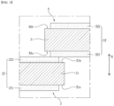
FIG. 3 is a schematic front view illustrating a shape where a first unit cell is bonded to a second unit cell, in a solar cell obtained according to the present invention. -
FIG. 4 is a schematic front view illustrating a shape before a first unit cell is bonded to a second unit cell, in an example of a solar cell obtained according to the present invention. -
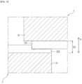
FIG. 5 is a schematic front view illustrating a shape after a first unit cell is bonded to a second unit cell, in an example of a solar cell obtained according to the present invention. -
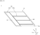
FIG. 6 is a schematic perspective view illustrating a first junction electrode and a first non-junction electrode formed in a first upper cell electrode, in a solar cell obtained according to the present invention. -
FIG. 7 is a schematic perspective view illustrating a second junction electrode and a second non-junction electrode formed in a second lower cell electrode, in a solar cell obtained according to the present invention. -
FIG. 8 is a schematic front view illustrating a shape before a second junction electrode is bonded to a first junction electrode, in a solar cell obtained according to the present invention. -
FIG. 9 is a schematic front view illustrating a shape where an inserting member is inserted into an inserting groove as a second junction electrode is bonded to a first junction electrode, in a solar cell obtained according to the present invention. -
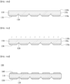
FIG. 10A is a schematic process front view illustrating a substrate preparing process of a method of manufacturing a solar cell according to the present invention. -
FIG. 10B is a schematic process front view illustrating a first electrode forming process of a method of manufacturing a solar cell according to the present invention. -
FIG. 10C is a schematic process front view illustrating a first curing process of a method of manufacturing a solar cell according to the present invention. -
FIG. 10D is a schematic process front view illustrating a second electrode forming process of a method of manufacturing a solar cell according to the present invention. -
FIG. 10E is a schematic process front view illustrating a division process of a method of manufacturing a solar cell according to the present invention. - Advantages and features of the present invention, and implementation methods thereof will be clarified through following embodiments described with reference to the accompanying drawings. The present invention may, however, be embodied in different forms and should not be construed as limited to the embodiments set forth herein. Rather, these embodiments are provided so that present invention will be thorough and complete, and will fully convey the scope of the present invention to those skilled in the art. Furthermore, the present invention is only defined by scopes of claims.
- A shape, a size, a ratio, an angle, and a number disclosed in the drawings for describing embodiments of the present invention are merely an example, and thus, the present invention is not limited to the illustrated details. Like reference numerals refer to like elements throughout. In the following description, when the detailed description of the relevant known technology is determined to unnecessarily obscure the important point of the present invention, the detailed description will be omitted. In a case where 'comprise', 'have', and 'include' described in the present specification are used, another part may be added unless 'only-' is used. The terms of a singular form may include plural forms unless referred to the contrary.
- In construing an element, the element is construed as including an error range although there is no explicit description.
- In describing a position relationship, for example, when a position relation between two parts is described as 'on~', 'over-', `under~', and 'next-', one or more other parts may be disposed between the two parts unless 'just' or 'direct' is used.
- In describing a time relationship, for example, when the temporal order is described as 'after-', `subsequent~', 'next-', and 'before-', a case which is not continuous may be included unless 'just' or 'direct' is used.
- It will be understood that, although the terms "first", "second", etc. may be used herein to describe various elements, these elements should not be limited by these terms. These terms are only used to distinguish one element from another. For example, a first element could be termed a second element, and, similarly, a second element could be termed a first element, without departing from the scope of the present invention.
- Features of various embodiments of the present invention may be partially or overall coupled to or combined with each other, and may be variously inter-operated with each other and driven technically as those skilled in the art can sufficiently understand. The embodiments of the present invention may be carried out independently from each other, or may be carried out together in co-dependent relationship.
- Hereinafter, an embodiment of a
solar cell 1 obtained according to the present invention will be described in detail with reference to the accompanying drawings. Aunit cell 10 is included in thesolar cell 1, and thus, will be described along with describing an embodiment of thesolar cell 1. Hatchings and dots illustrated inFIGS. 1 to 10E do not illustrate a cross-sectional surface and are illustrated for distinguishing elements. - Referring to
FIG. 1 , thesolar cell 1 converts light energy of sunlight into electrical energy. Thesolar cell 1 may be implemented as a wafer type solar cell and a thin film type solar cell. Hereinafter, an embodiment where thesolar cell 1 is implemented as a wafer type solar cell will be described, but based thereon, it is obvious to those skilled in the art that thesolar cell 1 is implemented as a thin film type solar cell. - Referring to
FIG. 1 , thesolar cell 1 may be manufactured as a module type where a plurality ofunit cells 10 are bonded to one another. Each of theunit cells 10 is manufactured by using one of a plurality of pieces which are formed by dividing a base substrate 100 (illustrated inFIG. 10D ). In thesolar cell 1, thebase substrate 100 may be in a state before being divided into theunit cells 10. Thebase substrate 100 includes a substrate 110 (illustrated inFIG. 10A ), a first base electrode 130 (illustrated inFIG. 10B ) formed on onesurface 110a of thesubstrate 110, and a second base electrode 140 (illustrated inFIG. 10D ) formed on theother surface 110b of thesubstrate 110. InFIG. 1 , thesolar cell 1 is illustrated as including fiveunit cells solar cell 1 according to the present invention may include two to fourunit cells 10 or six ormore unit cells 10. Each of theunit cells 10 may be implemented to be approximately equal, except for a disposed position thereof. - Referring to
FIGS. 1 and 2 , each of theunit cells 10 includes aunit substrate 11 and acell electrode 12. - The
unit substrate 11 is formed by dividing the base substrate 100 (illustrated inFIG. 10D ). Theunit substrate 11 may have a certain conductive polarity. Theunit substrate 11 may be formed to be equal to the number of pieces which are formed by dividing onebase substrate 100. For example, when thebase substrate 100 is divided into five pieces, theunit substrate 11 may be formed as five. Theunit substrate 11 may be a portion of the substrate 110 (illustrated inFIG. 10A ). - The
cell electrode 12 is formed on theunit substrate 11. Thecell electrode 12 may have conductivity. Thecell electrode 12 may be formed of a metal material, having good conductivity, such as Ag, Al, Ag+Al, Ag+Mg, Ag+Mn, Ag+Sb, Ag+Zn, Ag+Mo, Ag+Ni, Ag+Cu, or Ag+Al+Zn. - The
cell electrode 12 includes alower cell electrode 121 and anupper cell electrode 122. - The
lower cell electrode 121 is formed on onesurface 11a of theunit substrate 11. The onesurface 11a of theunit substrate 11 may be a surface of theunit substrate 11 facing a downward direction in which a height of thesolar cell 1 according to the present invention is approximately lowered. The onesurface 11a of theunit substrate 11 may be a surface of theunit substrate 11 facing an upward direction which is a direction opposite to the downward direction. Thelower cell electrode 121 may be one electrode of the first base electrode 130 (illustrated inFIG. 10B ). - The
upper cell electrode 122 is formed on theother surface 11b of theunit substrate 11. When the onesurface 11a of theunit substrate 11 is the surface of theunit substrate 11 facing the downward direction, theother surface 11b of theunit substrate 11 may be a surface of theunit substrate 11 facing the upward direction. Hereinafter, an example where "one surface" and "the other surface" are surfaces of specific elements facing the downward direction and the upward direction will be described. Also, the terms "upper" and "lower" described in the present specification are for distinguishing elements, and it is obvious to those skilled in the art that the terms "upper" and "lower" do not denote a specific direction. Theupper cell electrode 122 may be one electrode of the second base electrode 140 (illustrated inFIG. 10D ). - One of the
upper cell electrode 122 and thelower cell electrode 121 is formed in an uncured state PC. Therefore, thesolar cell 1 according to the present invention may implement a bonding force for bonding theunit cells 10 through an electrode having the uncured state PC. The uncured state PC is a state where an electrode has a bonding force. Theelectrodes upper cell electrode 122 and thelower cell electrode 121 is in a cured state HC, the other electrode is formed in the uncured state PC. Even in this case, thesolar cell 1 according to the present invention may implement a bonding force for bonding theunit cells 10 through an electrode having the uncured state PC. The cured state HC is a state where an electrode does not have a bonding force. Theelectrodes - Referring to
FIGS. 3 to 9 , asolar cell 1 obtained according to the present invention includes afirst unit cell 2 and asecond unit cell 3. - The
first unit cell 2 is one of theunit cells 10. Thefirst unit cell 2 is manufactured by using one of a plurality of pieces which are formed by dividing thebase substrate 100. Power generated by thesolar cell 1 according to the present invention may move to thesecond unit cell 3 through thefirst unit cell 2. - Referring to
FIG. 3 , thefirst unit cell 2 includes afirst unit substrate 21 and afirst cell electrode 22. - The
first unit substrate 21 is a portion of the substrate 110 (illustrated inFIG. 10A ). Thefirst unit substrate 21 is formed by dividing thebase substrate 100. Thefirst unit substrate 21 may have a certain conductive polarity. - The
first cell electrode 22 is formed on thefirst unit substrate 21. Thefirst cell electrode 22 is formed on each of onesurface 21a and theother surface 21b of thefirst unit substrate 21. Thefirst cell electrode 22 may have conductivity. Thefirst cell electrode 22 may be formed of a material such as Ag, Al, Ag+Al, Ag+Mg, Ag+Mn, Ag+Sb, Ag+Zn, Ag+Mo, Ag+Ni, Ag+Cu, or Ag+Al+Zn. - The
first cell electrode 22 includes a firstlower cell electrode 221 and a firstupper cell electrode 222. - The first
lower cell electrode 221 is formed on onesurface 21a of thefirst unit substrate 21. The firstlower cell electrode 221 may be formed on the onesurface 21a of thefirst unit substrate 21 disposed in the downward direction. The firstlower cell electrode 221 may be one electrode of the first base electrode 130 (illustrated inFIG. 10B ). The firstlower cell electrode 221 may be formed in one state of the cured state HC and the uncured state PC. - The first
upper cell electrode 222 is formed on theother surface 21b of thefirst unit substrate 21. The firstupper cell electrode 222 may be formed on theother surface 21b of thefirst unit substrate 21 disposed in the upward direction. The firstupper cell electrode 222 may be one electrode of the second base electrode 140 (illustrated inFIG. 10D ). The firstupper cell electrode 222 is formed in a state which differs from the first lower cell electrode. For example, when the firstlower cell electrode 221 is in the cured state HC, the firstupper cell electrode 222 is formed in the uncured state PC. When the firstlower cell electrode 221 is in the uncured state PC, the firstupper cell electrode 222 is formed in the cured state HC. - The
second unit cell 3 is one unit cell coupled to thefirst unit cell 2 among theunit cells 10. Thesecond unit cell 3 may be coupled to thefirst unit cell 2 in the upward direction of thefirst unit cell 2. Thesecond unit cell 3 is manufactured by using one of a plurality of pieces which are formed by dividing thebase substrate 100. - The
second unit cell 3 includes asecond unit substrate 31 and asecond cell electrode 32. - The
second unit substrate 31 is a portion of the substrate 110 (illustrated inFIG. 10A ). Thesecond unit substrate 31 is formed by dividing the base substrate 100 (illustrated in FIG. 1C). Thesecond unit substrate 31 may have a certain conductive polarity. - The
second cell electrode 32 is formed on thesecond unit substrate 31. Thesecond cell electrode 32 is formed on each of onesurface 31a and theother surface 31b of thesecond unit substrate 31. Thesecond cell electrode 32 may have conductivity. Thesecond cell electrode 32 may be formed of a material such as Ag, Al, Ag+Al, Ag+Mg, Ag+Mn, Ag+Sb, Ag+Zn, Ag+Mo, Ag+Ni, Ag+Cu, or Ag+Al+Zn. - The
second cell electrode 32 and thefirst cell electrode 22 are bonded to each other without a bonding material, and thus, couple thesecond unit cell 3 to thefirst unit cell 2. That is, as thesecond cell electrode 32 and thefirst cell electrode 22 are bonded to each other, thesecond unit cell 3 is coupled to thefirst unit cell 2. Accordingly, thesolar cell 1 obtained according to the present invention may realize the following effects. - First, the
solar cell 1 obtained according to the present invention is implemented so that theunit cells cell electrodes unit cells 10 are bonded to each other by using a bonding material, in thesolar cell 1, a series of process of distributing a bonding material is omitted in a process of manufacturing a solar cell. Accordingly, in thesolar cell 1, a time taken in manufacturing a solar cell may be reduced, and thus, the productivity of solar cells may increase. - Second, the
solar cell 1 obtained according to the present invention is implemented so that theunit cells solar cell 1 may fundamentally prevent the power generating efficiency of the solar cell from being reduced by the resistance of the bonding material, thereby enhancing the quality of a finished solar cell. - The
second cell electrode 32 and thefirst cell electrode 22 may be formed of the same material, and thus, may be bonded to each other. For example, thesecond cell electrode 32 and thefirst cell electrode 22 may all be formed of an Ag material. Therefore, thesolar cell 1 obtained according to the present invention is implemented to decrease an internal resistance thereof. This is because a resistance is more reduced in a case, where power moves to the same material, than a case where power moves to different materials, in a process where power moves to thefirst cell electrode 22 and thesecond cell electrode 32. Accordingly, thesolar cell 1 obtained according to the present invention may more increase the power generating efficiency of a solar cell. - The
second cell electrode 32 includes a secondlower cell electrode 321 and a secondupper cell electrode 322. - The second
lower cell electrode 321 is formed on onesurface 31a of thesecond unit substrate 31. The secondlower cell electrode 321 may be formed on the onesurface 31a of thesecond unit substrate 31 disposed in the downward direction. The secondlower cell electrode 321 may be one electrode of thefirst base electrode 130. The secondlower cell electrode 321 is formed in one state of the cured state HC and the uncured state PC. - The second
upper cell electrode 322 is formed on theother surface 31b of thesecond unit substrate 31. The secondupper cell electrode 322 may be formed on theother surface 31b of thesecond unit substrate 31 in the upward direction. The secondupper cell electrode 322 may be one electrode of thesecond base electrode 140. When the secondlower cell electrode 321 is in the cured state HC, the secondupper cell electrode 322 is formed in the uncured state PC. When the secondlower cell electrode 321 is in the uncured state PC, the secondupper cell electrode 322 is formed in the cured state HC. - The
solar cell 1, as illustrated inFIG. 3 , is implemented so that the secondlower cell electrode 321 and the firstupper cell electrode 222 are bonded to each other, and thus, thesecond unit cell 3 is coupled to thefirst unit cell 2. Hereinafter, an example where the secondlower cell electrode 321 and the firstupper cell electrode 222 are bonded to each other and thus thesecond unit cell 3 is coupled to thefirst unit cell 2 will be described, but this is an example and thesecond unit cell 3 may be coupled to thefirst unit cell 2 as the secondupper cell electrode 322 and the firstlower cell electrode 221 are bonded to each other. - At least one of the second
lower cell electrode 321 and the firstupper cell electrode 222 is formed in the uncured state PC. Therefore, thesolar cell 1 may implement a bonding force for coupling theunit cells lower cell electrode 321 and the firstupper cell electrode 222 is formed in the uncured state PC, the other electrode is formed in the cured state HC, and thus, thesecond unit cell 3 is coupled to thefirst unit cell 2. - Referring to
FIGS. 4 and5 , the firstupper cell electrode 222 is formed in the uncured state PC, and thus, the secondlower cell electrode 321 is bonded thereto, whereby a thickness thereof may be reduced. Therefore, in thesolar cell 1, a total thickness thereof may be reduced, and thus, a distance by which a generated power moves may be reduced. Accordingly, thesolar cell 1 may be implemented to decrease a total resistance thereof. The thickness may be a length with respect to a first axial direction (an X-axis direction) which corresponds to a direction parallel to each of the upward direction and the downward direction and corresponds to the same direction as a direction in which thesecond unit cell 3 is apart from thefirst unit cell 2. - For example, as illustrated in
FIGS. 4 and5 , when the firstupper cell electrode 222 is formed to have a first thickness D1 and the secondlower cell electrode 321 is formed to have a second thickness D2, a third thickness D3 which is formed as the secondlower cell electrode 321 and the firstupper cell electrode 222 are bonded to each other may have a value which is less than a sum of the first thickness D1 and the second thickness D2. This is because one of the firstupper cell electrode 222 and the secondlower cell electrode 321 is formed in the uncured state PC. Accordingly, thesolar cell 1 obtained according to the present invention may be implemented to decrease a total thickness thereof. The third thickness D3 may be a separation distance between thesecond unit cell 3 and thefirst unit cell 2 with respect to the first axial direction (the X-axis direction). InFIG. 4 , it is illustrated that the firstupper cell electrode 222 is formed in the uncured state PC, but this is an example and the third thickness D3 may decrease as the secondlower cell electrode 321 is formed in the uncured state PC. - When one of the second
lower cell electrode 321 and the firstupper cell electrode 222 is formed in the uncured state PC, as illustrated inFIG. 5 , the secondlower cell electrode 321 and the firstupper cell electrode 222 may be disposed to partially overlap each other with respect to the first axial direction (the X-axis direction). Accordingly, a total thickness of thesolar cell 1 obtained according to the present invention may be reduced. - Hereinafter, an embodiment of a pattern of each of the first
upper cell electrode 222 and the secondlower cell electrode 321 will be described with reference to the accompanying drawings. When thesecond unit cell 3 is coupled to thefirst unit cell 2 as the secondupper cell electrode 322 and the firstlower cell electrode 221 are bonded to each other, the firstlower cell electrode 221 may be implemented to be approximately equal to the below-described secondlower cell electrode 321, and the secondupper cell electrode 322 may be implemented to be approximately equal to the firstupper cell electrode 222. - Referring to
FIG. 6 , the firstupper cell electrode 222 may include afirst junction electrode 2221. - The second
lower cell electrode 321 is bonded to thefirst junction electrode 2221. Thefirst junction electrode 2221 may be one electrode of the firstupper cell electrode 222 bonded to the secondlower cell electrode 321. Thefirst junction electrode 2221 may be coupled to thefirst unit substrate 21. Thefirst junction electrode 2221 may be formed in the cured state HC. - The
first junction electrode 2221 may include a first junction surface 1A and an inserting groove G. - The first junction surface 1A (illustrated in
FIG. 8 ) may be one surface of thefirst junction electrode 2221 facing the secondlower cell electrode 321. In this case, the other surface of thefirst junction electrode 2221 may face thefirst unit substrate 21. The secondlower cell electrode 321 may be bonded to the first junction surface 1A. - The inserting groove G is formed in the first junction surface 1A. The inserting groove G may be formed by a process of processing a certain deep groove from the first junction surface 1A. The inserting groove G may be formed to have the same size as that of the first
upper cell electrode 222 with respect to the first axial direction (the X-axis direction). InFIG. 6 , it is illustrated that fourteen inserting grooves G are formed in the first junction surface 1A, but this is an example and one to thirteen inserting grooves G or fifteen or more inserting grooves G may be formed in the first junction surface 1A. - Referring to
FIG. 6 , thefirst junction electrode 2221 may include a first junction finger bar 1F. - The first junction finger bar 1F may perform a function of moving power, generated from the
first unit substrate 21, to the secondlower cell electrode 321. The first junction finger bar 1F is formed with the inserting groove G being disposed inward therefrom. The first junction finger bar 1F may include a first junction finger member formed in a second axial direction (a Y-axis direction) and a second junction finger member formed in a third axial direction (a Z-axis direction) vertical to the second axial direction (the Y-axis direction). The second junction finger member and the first junction finger member may be coupled to each other. The second junction finger member and the first junction finger member may be disposed to surround the inserting groove G. For example, two second junction finger members and two first junction finger members may be disposed outside the inserting groove G. One second junction finger member and two first junction finger members may also be disposed outside the inserting groove G.FIG. 6 illustrates three first junction finger members and twelve second junction finger members. The second axial direction (the Y-axis direction) may be a direction vertical to the first axial direction (the X-axis direction). The third axial direction (the Z-axis direction) may be a direction vertical to each of the second axial direction (the Y-axis direction) and the first axial direction (the X-axis direction). - Referring to
FIG. 6 , the firstupper cell electrode 222 may include afirst non-junction electrode 2222. - The
first non-junction electrode 2222 is coupled to thefirst junction electrode 2221. Thefirst non-junction electrode 2222 may be coupled to thefirst junction electrode 2221 and may perform a function of moving the power, generated from thefirst unit substrate 21, to thefirst junction electrode 2221. Thefirst non-junction electrode 2222 may be one electrode of the firstupper cell electrode 222 which is not bonded to the secondlower cell electrode 321. Thefirst non-junction electrode 2222 may be coupled to thefirst unit substrate 21. Thefirst non-junction electrode 2222 may be formed in the cured state HC which is the same state as that of thefirst junction electrode 2221. - The
first non-junction electrode 2222 may include a plurality of first non-junction finger bars 10F which are disposed apart from one another. The first non-junction finger bars 10F may be disposed apart from one another with respect to the second axial direction (the Y-axis direction). The first non-junction finger bars 10F may be formed to extend in the third axial direction (the Z-axis direction). The first non-junction finger bars 10F may be formed to have a linear shape in the third axial direction (the Z-axis direction). The first non-junction finger bars 10F may be coupled to thefirst junction electrode 2221. The first non-junction finger bars 10F may perform a function of moving the generated power to thefirst junction electrode 2221.FIG. 6 illustrates three first non-junction finger bars 10F. - Referring to
FIGS. 7 to 9 , the secondlower cell electrode 321 may include asecond junction electrode 3211. - The
second junction electrode 3211 is bonded to thefirst junction electrode 2221. Thesecond junction electrode 3211 may be one electrode of the secondlower cell electrode 321 bonded to thefirst junction electrode 2221. Thesecond junction electrode 3211 may be coupled to thesecond unit substrate 31. Thesecond junction electrode 3211 may be formed in the cured state HC. - Referring to
FIGS. 7 and8 , thesecond junction electrode 3211 may include asecond junction surface 2A. - The
second junction surface 2A may be one surface of thesecond junction electrode 3211 facing the firstupper cell electrode 222. The other surface of thesecond junction electrode 3211 may face thesecond unit substrate 31. Thesecond junction surface 2A may be bonded to thefirst junction electrode 2221. Thesecond junction surface 2A may be formed to have a flat shape before thesecond junction electrode 3211 and thefirst junction electrode 2221 are bonded to each other. That is, thesecond junction surface 2A may be formed in a flat shape having no curve before thesecond junction electrode 3211 and thefirst junction electrode 2221 are bonded to each other. - Referring to
FIG. 9 , thesecond junction electrode 3211 may include an inserting member I. - The inserting member I is inserted into the inserting groove G as the
second junction electrode 3211 is bonded to thefirst junction electrode 2221. Therefore, thesolar cell 1 according to the present invention may be implemented so that thesecond junction electrode 3211 is supported by thefirst junction electrode 2221. Accordingly, thesolar cell 1 according to the present invention may enhance a bonding force between thesecond junction electrode 3211 and thefirst junction electrode 2221, thereby increasing a coupling force between thefirst unit cell 2 and thesecond unit cell 3. The inserting member I may be formed in the uncured state PC and may be inserted into the inserting groove G. - The inserting member I may be formed in a shape corresponding to the inserting groove G. The
second junction electrode 3211 may include a plurality of inserting members I equal to the number of inserting grooves G. - Hereinabove, it has been described that the
first junction electrode 2221 includes the inserting groove G and thesecond junction electrode 3211 includes the inserting member I, but it should be understood that this is an example and it is obvious to those skilled in the art that thefirst junction electrode 2221 includes the inserting member I and thesecond junction electrode 3211 includes the inserting groove G. - Referring to
FIGS. 7 to 9 , the secondlower cell electrode 321 may include asecond non-junction electrode 3212. - The
second non-junction electrode 3212 is coupled to thesecond junction electrode 3211. Thesecond non-junction electrode 3212 may be coupled to thesecond junction electrode 3211 and may perform a function of moving power generated from thesecond unit substrate 31. Thesecond non-junction electrode 3212 may be one electrode of the secondlower cell electrode 321 which is not bonded to the firstupper cell electrode 222. Thesecond non-junction electrode 3212 may be coupled to thesecond unit substrate 31. Thesecond non-junction electrode 3212 may be formed in the uncured state PC which is the same state as that of thesecond junction electrode 3211. - The
second non-junction electrode 3212 may include a plurality of second non-junction finger bars 20F which are disposed apart from one another. The second non-junction finger bars 20F may be disposed apart from one another with respect to the second axial direction (the Y-axis direction). The second non-junction finger bars 20F may be formed to extend in the third axial direction (the Z-axis direction). The second non-junction finger bars 20F may be coupled to thesecond junction electrode 3211. The second non-junction finger bars 20F may perform a function of moving the power generated from thesecond unit substrate 31.FIG. 7 illustrates three second non-junction finger bars 20F. - Hereinafter, an embodiment of a method of manufacturing a solar cell according to the present invention will be described in detail with reference to the accompanying drawings.
- Referring to
FIG. 10A , a method of manufacturing a solar cell according to the present invention may include a substrate preparing process. - The substrate preparing process is a process of preparing the
substrate 10 where a plurality ofdivision parts 120 for dividing thesubstrate 110 into a plurality of pieces are formed. The substrate preparing process may be performed by a substrate loading apparatus (not shown) which loads thesubstrate 110 into a processing space (not shown) for manufacturing a solar cell. The processing space may accommodate a plurality of manufacturing apparatuses needed for manufacturing a solar cell and may be wholly implemented as a chamber. - The
substrate 110 may have a certain conductive polarity. For example, thesubstrate 110 may be formed of an N-type silicon wafer or a P-type silicon wafer. Although not shown, the onesurface 110a of thesubstrate 110 may be formed in a concave-convex structure. Thesubstrate 110 may include a bottom surface disposed in the downward direction, a top surface disposed in the upward direction, and aside surface 110c connected to each of the bottom surface and the top surface of thesubstrate 110. In this case, the onesurface 110a of thesubstrate 110 may correspond to one of the bottom surface of thesubstrate 110, the top surface of thesubstrate 110, and theside surface 110c of thesubstrate 110. For example, when the onesurface 110a of thesubstrate 110 corresponds to the bottom surface of thesubstrate 110, theother surface 110b of thesubstrate 110 corresponds to the top surface of thesubstrate 110. In this case, each of a plurality of thin film layers formed on the onesurface 110a of thesubstrate 110 and theother surface 110b of thesubstrate 110 may be formed in a concave-convex structure. - The
division parts 120 are for dividing thesubstrate 110 into the plurality of pieces. Thedivision parts 120 may be formed on the onesurface 110a of thesubstrate 110. Thedivision parts 120 may be formed through a scribing process of processing a certain deep groove from the onesurface 110a of thesubstrate 110. The scribing process may be performed by a scribing apparatus (not shown) which irradiates a laser onto thesubstrate 110 to remove a certain region of thesubstrate 110. InFIG. 10A , it is illustrated that the scribing process is performed on the onesurface 110a of thesubstrate 110, but this is an example and the scribing process may be performed on theother surface 110b of thesubstrate 110. Also, in the present specification, an example where thedivision parts 120 are formed through the scribing process has been described, but this is an example and thedivision parts 120 may be formed by a process of digesting thesubstrate 110 into an etching bath (not shown), a dry etching process, or a process using a mask. In a case for dividing thesubstrate 110 into five pieces, as illustrated inFIG. 10A , fourdivision parts 120 may be formed on the onesurface 110a of thesubstrate 110. - Although not shown, one or more thin film layers may be formed on the
substrate 110. Hereinafter, an example of a thin film layer formed on thesubstrate 110 will be described. - First, a first thin film layer may be formed on the
substrate 110. A process of forming the first thin film layer may be performed after the scribing process. The first thin film layer may be a semiconductor layer which is formed as a thin film type on thesubstrate 110. The first thin film layer may form a PN junction along with thesubstrate 110. Therefore, in a case where thesubstrate 110 is formed of an N-type silicon wafer, the first thin film layer may be a P-type semiconductor layer. The first thin film layer may be formed by using a chemical vapor deposition (CVD) process and/or the like. The first thin film layer may be formed in a PIN structure where a P-type semiconductor material, an I-type semiconductor material, and an N-type semiconductor material are sequentially stacked. As described above, when the first thin film layer is formed in the PIN structure, the I-type semiconductor material is depleted by the P-type semiconductor material and the N-type semiconductor material, and thus, an electric field is generated therein and a hole and an electron generated from sunlight are drifted by the electric field and are collected into the P-type semiconductor material and the N-type semiconductor material. In a case where the first thin film layer is formed in the PIN structure, it is preferable that the P-type semiconductor material is formed on the first thin film layer, and then, the I-type semiconductor material and the N-type semiconductor material are formed. The reason is for that the P-type semiconductor material is formed close to a light receiving surface so as to collection efficiency based on incident light because the drift mobility of a hole is lower than the drift mobility of an electron generally. The method of manufacturing a solar cell according to the present invention may form the first thin film layer to have a stacked structure. For example, the method of manufacturing a solar cell according to the present invention may form the first thin film layer to have a stacked structure having a tandem(PIN/PIN) type or a triple(PIN/PIN/PIN) type. The first thin film layer may be formed on at least one of the onesurface 110a, theother surface 110b, and the side surface of thesubstrate 110, or may be formed on each of the onesurface 110a, theother surface 110b, and the side surface of thesubstrate 110. - Subsequently, a second thin film layer is formed on the first thin film layer. A process of forming the second thin film layer may be performed after a process of forming the first thin film layer. The second thin film layer may be a transparent conductive layer. For example, the second thin film layer may be a transparent conductive oxide (TCO) layer. The first thin film layer may protect the first thin film layer, collect a carrier (for example, a hole (+)) generated in the
substrate 110, and move the collected carrier in the upward direction. The second thin film layer may be formed of a transparent conductive material such as indium tin oxide (ITO), ZnOH, ZnO:B, ZnO:Al, SnO2, or SnO2:F. The second thin film layer may be formed of a transparent conductive material such as ZnO, ZnO:B, ZnO:Al, or Ag by using a sputtering process or a metal organic CVD (MOCVD) process. The second thin film layer has a function which scatters sunlight to allow the sunlight to travel at various angles, and thus, increases a ratio of light re-incident on the first thin film layer. - Subsequently, a third thin film layer is formed on the second thin film layer. A process of forming the third thin film layer may be performed after a process of forming the second thin film layer. In a case which forms the third thin film layer on the second thin film layer, the first thin film layer may be implemented as an intrinsic semiconductor layer, the second thin film layer may be implemented as a semiconductor layer, and the third thin film layer may be implemented as a transparent conductive layer. In this case, the plurality of thin film layers may be formed by using a plasma enhanced CVD (PECVD) process and a sputtering process.
- The method of manufacturing a solar cell according to the present invention may selectively form the first thin film layer, the second thin film layer, and the third thin film layer. That is, the method of manufacturing a solar cell according to the present invention may form one or more of the first thin film layer, the second thin film layer, and the third thin film layer, or may not form all of the first thin film layer, the second thin film layer, and the third thin film layer.
- Referring to
FIG. 10B , the method of manufacturing a solar cell according to the present invention includes a first electrode forming process. - The first electrode forming process is a process of forming a plurality of
first base electrodes 130 having conductivity on the onesurface 110a of thesubstrate 110. The first electrode forming process may be performed after the substrate preparing process. Thefirst base electrode 130 formed by performing the first electrode forming process may be formed of a material such as Ag, Al, Ag+Al, Ag+Mg, Ag+Mn, Ag+Sb, Ag+Zn, Ag+Mo, Ag+Ni, Ag+Cu, or Ag+Al+Zn. InFIG. 10B , it is illustrated that the first electrode forming process is performed on the onesurface 110a of thesubstrate 110, but this is an example and the first electrode forming process may be performed on theother surface 110b of thesubstrate 110. - Referring to
FIG. 10C , the method of manufacturing a solar cell according to the present invention includes a first curing process. - The first curing process is a process of curing the
first base electrode 130. The first curing process may be performed after the first electrode forming process. The first curing process may be performed by a heating apparatus (not shown) which heats thefirst base electrode 130. As the first curing process is performed, thefirst base electrode 130 may be formed in the cured state HC. - Referring to
FIG. 10D , the method of manufacturing a solar cell according to the present invention includes a second electrode forming process. - The second electrode forming process is a process of forming a plurality of
second base electrodes 140, having conductivity and the uncured state PC, on theother surface 110b of thesubstrate 110. The second electrode forming process may be performed after the first electrode forming process. Thesecond base electrode 140 formed by performing the second electrode forming process may be formed of a material such as Ag, Al, Ag+Al, Ag+Mg, Ag+Mn, Ag+Sb, Ag+Zn, Ag+Mo, Ag+Ni, Ag+Cu, or Ag+Al+Zn. InFIG. 10D , it is illustrated that the second electrode forming process is performed on theother surface 110b of thesubstrate 110, but this is an example and the second electrode forming process may be performed on the onesurface 110a of thesubstrate 110. - The method of manufacturing a solar cell according to the present invention is implemented not to include a process of curing the
second base electrode 140 after the second electrode forming process is performed. Accordingly, the method of manufacturing a solar cell according to the present invention may implement a bonding force which bonds theunit cells 10 through thesecond base electrode 140 having the uncured state PC. - Referring to
FIG. 10E , the method of manufacturing a solar cell according to the present invention includes a division process. - The division process is a process of dividing the
substrate 110 into a plurality of pieces through thedivision parts 120 to form theunit cells 10. That is, the division process is a process of dividing thebase substrate 100 through thedivision parts 120 to form a plurality ofunit cells 10. The division process may be performed by a division apparatus (not shown) which applies an external force, such as a bending force, to thebase substrate 100. The division process may be performed after the second electrode forming process. In a case for dividing thebase substrate 100 into N (where N is an integer of 2 or more) number ofunit cells 10, the division process may be performed N-1 times. For example, as illustrated inFIG. 10E , in a case for dividing thebase substrate 100 into fiveunit cells 10, the division process may be performed four times. - Referring again to
FIG. 1 , the method of manufacturing a solar cell according to the present invention includes a bonding process. - The bonding process is a process of bonding the
unit cells 10 through thesecond base electrode 140 having the uncured state PC. The bonding process may be performed by a bonding apparatus (not shown) which moves and bonds the dividedunit cells 10. The bonding process is performed after the division process. In a case where thebase substrate 100 has been divided into N number ofunit cells 10, the bonding process may be performed N-1 times. For example, as illustrated inFIG. 10E , in a case where thebase substrate 100 has been divided into fiveunit cells 10, the bonding process may be performed four times. - Although not shown, the method of manufacturing a solar cell according to the present invention may include a second curing process.
- The second curing process is a process of curing the bonded
unit cells 10. The second curing process may be performed by the heating apparatus. The second curing process may be performed after the bonding process. As the second curing process is performed, thesolar cell 1 according to the present invention may be manufactured as a module type where theunit cells 10 are bonded to one another.
Claims (11)
- A method of manufacturing a solar cell, the method comprising:a substrate preparing process of preparing a substrate (110) where a plurality of division parts (120) for dividing the substrate into a plurality of pieces are formed;a first electrode forming process of forming a plurality of first base electrodes (130) having conductivity on one surface (110a) of the substrate;a first curing process of curing the first base electrode;a second electrode forming process of forming a plurality of second base electrodes (140), having conductivity and an uncured state, on the other surface (110b) of the substrate;a division process of dividing the substrate into a plurality of pieces through the division parts to form a plurality of unit cells (10) including a first unit cell (2) and a second unit cell (3), each of the first unit cell and the second unit cell including a first cell electrode in a cured state and a second cell electrode in an uncured state; anda bonding process of bonding the first unit cell and the second unit cell through the first cell electrode (222) of the first unit cell and the second cell electrode (321) of the second unit cell without a bonding material, the first unit cell the second unit cell partially overlapping each other, .
- The method of claim 1, further comprising a second curing process of curing the bonded unit cells after the bonding process is performed.
- The method of claim 1, whereinthe first cell electrode is formed to have a first thickness,the second cell electrode is formed to have a second thickness, anda third thickness between the first unit cell and the second unit cell, formed as the second cell electrode and the first cell electrode are bonded to each other, has a value which is less than a sum of the second thickness and the first thickness.
- The method of claim 1, wherein the second cell electrode and the first cell electrode are disposed to partially overlap each other with respect to a first axial direction in which the second unit cell and the first unit cell are apart from each other.
- The method of claim 1, wherein, when the second cell electrode and the first cell electrode are bonded to each other, the second cell electrode and the first cell electrode are formed to have the same thickness.
- The method of claim 1, wherein the first cell electrode and the second cell electrode are all formed of the same material.
- The method of claim 1, whereinthe first cell electrode comprises a first junction electrode (2221) bonded to the second cell electrode, andthe first junction electrode comprises a first junction surface (1A) facing the second cell electrode and an inserting groove (G) formed in the first junction surface.
- The method of claim 7, whereinthe first junction electrode further comprises a first junction finger bar (1F) formed with the inserting groove being disposed inward therefrom, andthe first junction finger bar comprises a first junction finger member, formed in a direction vertical to a direction in which the first unit cell and the second unit cell are apart from each other, and a second junction finger member coupled to the first junction finger member.
- The method cell of claim 7, whereinthe first cell electrode comprises a first non-junction electrode (2222) coupled to the first junction electrode, andthe first non-junction electrode comprises a plurality of first non-junction finger bars (10F) disposed apart from one another.
- The method of claim 7, whereinthe second cell electrode comprises a second junction electrode (3211) bonded to the first junction electrode,the second junction electrode comprises a second junction surface (2A) facing the first junction electrode, andthe second junction surface is formed to have a flat shape before the second junction electrode and the first junction electrode are bonded to each other.
- The method of claim 7, whereinthe second cell electrode comprises a second junction electrode bonded to the first junction electrode, andthe second junction electrode comprises an inserting member (I) bonded to the first junction electrode and inserted into the inserting groove as the second cell electrode is bonded to the first cell electrode.
Applications Claiming Priority (2)
| Application Number | Priority Date | Filing Date | Title |
|---|---|---|---|
| KR1020190129880A KR102678342B1 (en) | 2019-10-18 | 2019-10-18 | Unit Cell, Solar Cell and Method of Manufacturing Solar cell |
| PCT/KR2020/013035 WO2021075756A1 (en) | 2019-10-18 | 2020-09-25 | Unit cell, solar cell comprising same, and method for manufacturing solar cell |
Publications (3)
| Publication Number | Publication Date |
|---|---|
| EP4047669A1 EP4047669A1 (en) | 2022-08-24 |
| EP4047669A4 EP4047669A4 (en) | 2023-11-15 |
| EP4047669B1 true EP4047669B1 (en) | 2024-10-16 |
Family
ID=75537392
Family Applications (1)
| Application Number | Title | Priority Date | Filing Date |
|---|---|---|---|
| EP20876244.3A Active EP4047669B1 (en) | 2019-10-18 | 2020-09-25 | Method for manufacturing a solar cell |
Country Status (8)
| Country | Link |
|---|---|
| US (1) | US12094992B2 (en) |
| EP (1) | EP4047669B1 (en) |
| JP (1) | JP7603673B2 (en) |
| KR (1) | KR102678342B1 (en) |
| CN (1) | CN114365295B (en) |
| ES (1) | ES3000720T3 (en) |
| TW (1) | TWI890702B (en) |
| WO (1) | WO2021075756A1 (en) |
Family Cites Families (34)
| Publication number | Priority date | Publication date | Assignee | Title |
|---|---|---|---|---|
| JPH06140651A (en) * | 1992-10-27 | 1994-05-20 | Canon Inc | Solar cell module |
| EP1521309A1 (en) | 2003-10-02 | 2005-04-06 | Scheuten Glasgroep | Series connection of solar cells with integrated semiconductor bodies, method of production and photovoltaic module with series connection |
| KR20070101917A (en) * | 2006-04-12 | 2007-10-18 | 엘지전자 주식회사 | Thin-film solar cell and its manufacturing method |
| CN102341916B (en) * | 2009-03-02 | 2014-04-09 | 株式会社钟化 | Thin film solar cell module |
| JP2011086671A (en) * | 2009-10-13 | 2011-04-28 | Mitsubishi Chemicals Corp | Solar cell, and method for manufacturing the same |
| KR20120126224A (en) * | 2011-05-11 | 2012-11-21 | 한국전자통신연구원 | Method for Manufacturing Dye Sensitized Solar Cell |
| US20120325282A1 (en) | 2011-06-24 | 2012-12-27 | Solopower, Inc. | Solar cells with grid wire interconnections |
| US10741712B2 (en) * | 2012-02-15 | 2020-08-11 | Alta Devices, Inc. | Photovoltaic module containing shingled photovoltaic tiles and fabrication processes thereof |
| JP6045878B2 (en) * | 2012-10-22 | 2016-12-14 | 東レエンジニアリング株式会社 | Solar cell module |
| US20140124014A1 (en) | 2012-11-08 | 2014-05-08 | Cogenra Solar, Inc. | High efficiency configuration for solar cell string |
| US9780253B2 (en) | 2014-05-27 | 2017-10-03 | Sunpower Corporation | Shingled solar cell module |
| US10090430B2 (en) * | 2014-05-27 | 2018-10-02 | Sunpower Corporation | System for manufacturing a shingled solar cell module |
| CN103887368B (en) * | 2014-03-07 | 2016-05-11 | 京东方科技集团股份有限公司 | The integrated inline assembly of solar cell and preparation method, solar cell |
| JP6586080B2 (en) * | 2014-03-31 | 2019-10-02 | 株式会社カネカ | Solar cell module and manufacturing method thereof |
| KR102054420B1 (en) | 2014-05-27 | 2020-01-22 | 선파워 코포레이션 | Shingled solar cell module |
| KR102034888B1 (en) * | 2014-05-27 | 2019-11-08 | 선파워 코포레이션 | Shingled solar cell module |
| CN106206807A (en) * | 2014-10-31 | 2016-12-07 | 比亚迪股份有限公司 | Solaode chip arrays, solar module and preparation method thereof |
| US9991412B2 (en) * | 2014-12-05 | 2018-06-05 | Solarcity Corporation | Systems for precision application of conductive adhesive paste on photovoltaic structures |
| US9899546B2 (en) * | 2014-12-05 | 2018-02-20 | Tesla, Inc. | Photovoltaic cells with electrodes adapted to house conductive paste |
| US10861999B2 (en) * | 2015-04-21 | 2020-12-08 | Sunpower Corporation | Shingled solar cell module comprising hidden tap interconnects |
| CN109168324A (en) | 2015-12-30 | 2019-01-08 | 各星有限公司 | Advanced interconnection method for photovoltaic strings and modules |
| JP2019506004A (en) * | 2016-02-19 | 2019-02-28 | コーナー・スター・リミテッドCorner Star Limited | Connection module for photovoltaic modules |
| US10115838B2 (en) | 2016-04-19 | 2018-10-30 | Tesla, Inc. | Photovoltaic structures with interlocking busbars |
| JP6955915B2 (en) * | 2016-08-03 | 2021-10-27 | パナソニック株式会社 | Solar cell module and its manufacturing method |
| KR101895025B1 (en) * | 2016-11-14 | 2018-09-04 | 한국생산기술연구원 | Solar cell module and manufacturing method thereof |
| CN111095789B (en) * | 2016-12-08 | 2023-10-31 | 石刚 | Interconnection methods for shingled photovoltaic cells |
| CN106531829B (en) * | 2016-12-23 | 2018-11-30 | 泰州隆基乐叶光伏科技有限公司 | Interconnection structure and solar energy laminated batteries between a kind of solar energy laminated batteries piece |
| KR102459719B1 (en) | 2017-06-14 | 2022-10-27 | 상라오 징코 솔라 테크놀러지 디벨롭먼트 컴퍼니, 리미티드 | Solar cell, solar cell module and fabricating methods thereof |
| KR101976175B1 (en) * | 2017-09-20 | 2019-05-08 | 엘지전자 주식회사 | Compound semiconductor solar cell module and manufacturing methods thereof |
| CN108172648B (en) * | 2018-01-15 | 2024-04-12 | 晶澳太阳能有限公司 | Solar cell module and preparation process thereof |
| CN208706668U (en) * | 2018-03-22 | 2019-04-05 | 青海黄河上游水电开发有限责任公司光伏产业技术分公司 | A solar stack cell |
| CN108899387B (en) | 2018-07-03 | 2021-06-18 | 彭延岩 | A connection method of conductive adhesive and solar cell sheet that can be converted into an adhesive film instantly and online |
| CN110190145B (en) * | 2019-05-30 | 2024-09-06 | 泰州隆基乐叶光伏科技有限公司 | Back contact laminated solar cell string and manufacturing method, laminated solar cell module |
| CN110212048A (en) * | 2019-05-30 | 2019-09-06 | 泰州隆基乐叶光伏科技有限公司 | Back contacts lamination solar battery string and back contacts lamination solar module |
-
2019
- 2019-10-18 KR KR1020190129880A patent/KR102678342B1/en active Active
-
2020
- 2020-09-25 EP EP20876244.3A patent/EP4047669B1/en active Active
- 2020-09-25 ES ES20876244T patent/ES3000720T3/en active Active
- 2020-09-25 WO PCT/KR2020/013035 patent/WO2021075756A1/en not_active Ceased
- 2020-09-25 JP JP2022520556A patent/JP7603673B2/en active Active
- 2020-09-25 US US17/641,432 patent/US12094992B2/en active Active
- 2020-09-25 CN CN202080063331.3A patent/CN114365295B/en active Active
- 2020-10-16 TW TW109135974A patent/TWI890702B/en active
Also Published As
| Publication number | Publication date |
|---|---|
| CN114365295B (en) | 2024-12-31 |
| KR102678342B1 (en) | 2024-06-25 |
| US12094992B2 (en) | 2024-09-17 |
| WO2021075756A1 (en) | 2021-04-22 |
| JP7603673B2 (en) | 2024-12-20 |
| EP4047669A1 (en) | 2022-08-24 |
| US20220302332A1 (en) | 2022-09-22 |
| KR102678342B9 (en) | 2024-12-20 |
| KR20210046308A (en) | 2021-04-28 |
| JP2022552946A (en) | 2022-12-21 |
| ES3000720T3 (en) | 2025-03-03 |
| TWI890702B (en) | 2025-07-21 |
| CN114365295A (en) | 2022-04-15 |
| TW202129992A (en) | 2021-08-01 |
| EP4047669A4 (en) | 2023-11-15 |
Similar Documents
| Publication | Publication Date | Title |
|---|---|---|
| US9349897B2 (en) | Solar cell module and manufacturing method therefor | |
| EP3349255A1 (en) | Thin film-type solar cell and method for manufacturing same | |
| US20230361230A1 (en) | Thin film-type solar cell | |
| CN102194900B (en) | Solar cell and manufacture method thereof | |
| KR101092468B1 (en) | Solar cell and manufacturing method thereof | |
| KR20200122394A (en) | Solar cell module, glass building material, and manufacturing method of solar cell module | |
| KR101192345B1 (en) | Pattern Of The Electrode Of Solar Cell And Sollar Cell Comprising The Said Electrode Pattern | |
| US12094992B2 (en) | Unit cell, solar cell comprising same, and method for manufacturing solar cell | |
| KR20130039895A (en) | Thin flim solar cell module | |
| JP6971749B2 (en) | Manufacturing method of solar cell module and solar cell module | |
| KR102322346B1 (en) | Apparatus for Splitting Substrate | |
| KR102567037B1 (en) | A thin film type solar cell and Method of manufacturing the same | |
| KR102720681B1 (en) | Method of Manufacturing Solar Cell | |
| KR101940074B1 (en) | Solar Cell and method of manufacturing the same | |
| KR102723190B1 (en) | Method of Manufacturing Solar Cell | |
| KR101780771B1 (en) | A thin film type solar cell | |
| KR102629917B1 (en) | Method of Manufacturing Solar Cell | |
| KR20110128616A (en) | Tandem solar cell and manufacturing method thereof | |
| KR101573846B1 (en) | Thin-film solar cell, manufacturing method and manufacturing apparatus thereof | |
| KR102523303B1 (en) | Thin film type solor cell and Method of manufacturing the same | |
| KR20110095629A (en) | Solar cell and manufacturing method | |
| KR20130077010A (en) | A solar cell and a manufacturing method thereof |
Legal Events
| Date | Code | Title | Description |
|---|---|---|---|
| STAA | Information on the status of an ep patent application or granted ep patent |
Free format text: STATUS: THE INTERNATIONAL PUBLICATION HAS BEEN MADE |
|
| PUAI | Public reference made under article 153(3) epc to a published international application that has entered the european phase |
Free format text: ORIGINAL CODE: 0009012 |
|
| STAA | Information on the status of an ep patent application or granted ep patent |
Free format text: STATUS: REQUEST FOR EXAMINATION WAS MADE |
|
| 17P | Request for examination filed |
Effective date: 20220324 |
|
| AK | Designated contracting states |
Kind code of ref document: A1 Designated state(s): AL AT BE BG CH CY CZ DE DK EE ES FI FR GB GR HR HU IE IS IT LI LT LU LV MC MK MT NL NO PL PT RO RS SE SI SK SM TR |
|
| DAV | Request for validation of the european patent (deleted) | ||
| DAX | Request for extension of the european patent (deleted) | ||
| REG | Reference to a national code |
Ref legal event code: R079 Free format text: PREVIOUS MAIN CLASS: H01L0031042000 Ipc: H01L0031180000 Ref country code: DE Ref document number: 602020039712 Country of ref document: DE |
|
| A4 | Supplementary search report drawn up and despatched |
Effective date: 20231012 |
|
| RIC1 | Information provided on ipc code assigned before grant |
Ipc: H01L 21/78 20060101ALI20231006BHEP Ipc: H01L 31/05 20140101ALI20231006BHEP Ipc: H01L 31/0224 20060101ALI20231006BHEP Ipc: H01L 31/18 20060101AFI20231006BHEP |
|
| GRAP | Despatch of communication of intention to grant a patent |
Free format text: ORIGINAL CODE: EPIDOSNIGR1 |
|
| STAA | Information on the status of an ep patent application or granted ep patent |
Free format text: STATUS: GRANT OF PATENT IS INTENDED |
|
| INTG | Intention to grant announced |
Effective date: 20240527 |
|
| RIN1 | Information on inventor provided before grant (corrected) |
Inventor name: LIM, KYOUNG JIN Inventor name: YOON, YOUNG TAE Inventor name: SHIN, HYUN KYO Inventor name: SHIN, WON SUK Inventor name: SEO, JEONG HO Inventor name: MIN, SEON KI Inventor name: MUN, HYANG JU Inventor name: KANG, JUN YOUNG Inventor name: KIM, JUNG BAE |
|
| GRAS | Grant fee paid |
Free format text: ORIGINAL CODE: EPIDOSNIGR3 |
|
| GRAA | (expected) grant |
Free format text: ORIGINAL CODE: 0009210 |
|
| STAA | Information on the status of an ep patent application or granted ep patent |
Free format text: STATUS: THE PATENT HAS BEEN GRANTED |
|
| P01 | Opt-out of the competence of the unified patent court (upc) registered |
Free format text: CASE NUMBER: APP_46547/2024 Effective date: 20240812 |
|
| AK | Designated contracting states |
Kind code of ref document: B1 Designated state(s): AL AT BE BG CH CY CZ DE DK EE ES FI FR GB GR HR HU IE IS IT LI LT LU LV MC MK MT NL NO PL PT RO RS SE SI SK SM TR |
|
| REG | Reference to a national code |
Ref country code: GB Ref legal event code: FG4D |
|
| REG | Reference to a national code |
Ref country code: CH Ref legal event code: EP Ref country code: DE Ref legal event code: R096 Ref document number: 602020039712 Country of ref document: DE |
|
| REG | Reference to a national code |
Ref country code: IE Ref legal event code: FG4D |
|
| REG | Reference to a national code |
Ref country code: DE Ref legal event code: R079 Ref document number: 602020039712 Country of ref document: DE Free format text: PREVIOUS MAIN CLASS: H01L0031180000 Ipc: H10F0071000000 |
|
| REG | Reference to a national code |
Ref country code: LT Ref legal event code: MG9D |
|
| REG | Reference to a national code |
Ref country code: NL Ref legal event code: MP Effective date: 20241016 |
|
| REG | Reference to a national code |
Ref country code: ES Ref legal event code: FG2A Ref document number: 3000720 Country of ref document: ES Kind code of ref document: T3 Effective date: 20250303 |
|
| REG | Reference to a national code |
Ref country code: AT Ref legal event code: MK05 Ref document number: 1733680 Country of ref document: AT Kind code of ref document: T Effective date: 20241016 |
|
| PG25 | Lapsed in a contracting state [announced via postgrant information from national office to epo] |
Ref country code: NL Free format text: LAPSE BECAUSE OF FAILURE TO SUBMIT A TRANSLATION OF THE DESCRIPTION OR TO PAY THE FEE WITHIN THE PRESCRIBED TIME-LIMIT Effective date: 20241016 |
|
| PG25 | Lapsed in a contracting state [announced via postgrant information from national office to epo] |
Ref country code: NL Free format text: LAPSE BECAUSE OF FAILURE TO SUBMIT A TRANSLATION OF THE DESCRIPTION OR TO PAY THE FEE WITHIN THE PRESCRIBED TIME-LIMIT Effective date: 20241016 |
|
| PG25 | Lapsed in a contracting state [announced via postgrant information from national office to epo] |
Ref country code: PT Free format text: LAPSE BECAUSE OF FAILURE TO SUBMIT A TRANSLATION OF THE DESCRIPTION OR TO PAY THE FEE WITHIN THE PRESCRIBED TIME-LIMIT Effective date: 20250217 Ref country code: IS Free format text: LAPSE BECAUSE OF FAILURE TO SUBMIT A TRANSLATION OF THE DESCRIPTION OR TO PAY THE FEE WITHIN THE PRESCRIBED TIME-LIMIT Effective date: 20250216 Ref country code: HR Free format text: LAPSE BECAUSE OF FAILURE TO SUBMIT A TRANSLATION OF THE DESCRIPTION OR TO PAY THE FEE WITHIN THE PRESCRIBED TIME-LIMIT Effective date: 20241016 |
|
| PG25 | Lapsed in a contracting state [announced via postgrant information from national office to epo] |
Ref country code: FI Free format text: LAPSE BECAUSE OF FAILURE TO SUBMIT A TRANSLATION OF THE DESCRIPTION OR TO PAY THE FEE WITHIN THE PRESCRIBED TIME-LIMIT Effective date: 20241016 |
|
| PG25 | Lapsed in a contracting state [announced via postgrant information from national office to epo] |
Ref country code: BG Free format text: LAPSE BECAUSE OF FAILURE TO SUBMIT A TRANSLATION OF THE DESCRIPTION OR TO PAY THE FEE WITHIN THE PRESCRIBED TIME-LIMIT Effective date: 20241016 |
|
| PG25 | Lapsed in a contracting state [announced via postgrant information from national office to epo] |
Ref country code: NO Free format text: LAPSE BECAUSE OF FAILURE TO SUBMIT A TRANSLATION OF THE DESCRIPTION OR TO PAY THE FEE WITHIN THE PRESCRIBED TIME-LIMIT Effective date: 20250116 |
|
| PG25 | Lapsed in a contracting state [announced via postgrant information from national office to epo] |
Ref country code: GR Free format text: LAPSE BECAUSE OF FAILURE TO SUBMIT A TRANSLATION OF THE DESCRIPTION OR TO PAY THE FEE WITHIN THE PRESCRIBED TIME-LIMIT Effective date: 20250117 Ref country code: AT Free format text: LAPSE BECAUSE OF FAILURE TO SUBMIT A TRANSLATION OF THE DESCRIPTION OR TO PAY THE FEE WITHIN THE PRESCRIBED TIME-LIMIT Effective date: 20241016 Ref country code: LV Free format text: LAPSE BECAUSE OF FAILURE TO SUBMIT A TRANSLATION OF THE DESCRIPTION OR TO PAY THE FEE WITHIN THE PRESCRIBED TIME-LIMIT Effective date: 20241016 |
|
| PG25 | Lapsed in a contracting state [announced via postgrant information from national office to epo] |
Ref country code: PL Free format text: LAPSE BECAUSE OF FAILURE TO SUBMIT A TRANSLATION OF THE DESCRIPTION OR TO PAY THE FEE WITHIN THE PRESCRIBED TIME-LIMIT Effective date: 20241016 |
|
| PG25 | Lapsed in a contracting state [announced via postgrant information from national office to epo] |
Ref country code: RS Free format text: LAPSE BECAUSE OF FAILURE TO SUBMIT A TRANSLATION OF THE DESCRIPTION OR TO PAY THE FEE WITHIN THE PRESCRIBED TIME-LIMIT Effective date: 20250116 |
|
| PG25 | Lapsed in a contracting state [announced via postgrant information from national office to epo] |
Ref country code: SM Free format text: LAPSE BECAUSE OF FAILURE TO SUBMIT A TRANSLATION OF THE DESCRIPTION OR TO PAY THE FEE WITHIN THE PRESCRIBED TIME-LIMIT Effective date: 20241016 |
|
| PG25 | Lapsed in a contracting state [announced via postgrant information from national office to epo] |
Ref country code: DK Free format text: LAPSE BECAUSE OF FAILURE TO SUBMIT A TRANSLATION OF THE DESCRIPTION OR TO PAY THE FEE WITHIN THE PRESCRIBED TIME-LIMIT Effective date: 20241016 |
|
| REG | Reference to a national code |
Ref country code: DE Ref legal event code: R097 Ref document number: 602020039712 Country of ref document: DE |
|
| PG25 | Lapsed in a contracting state [announced via postgrant information from national office to epo] |
Ref country code: EE Free format text: LAPSE BECAUSE OF FAILURE TO SUBMIT A TRANSLATION OF THE DESCRIPTION OR TO PAY THE FEE WITHIN THE PRESCRIBED TIME-LIMIT Effective date: 20241016 |
|
| PG25 | Lapsed in a contracting state [announced via postgrant information from national office to epo] |
Ref country code: RO Free format text: LAPSE BECAUSE OF FAILURE TO SUBMIT A TRANSLATION OF THE DESCRIPTION OR TO PAY THE FEE WITHIN THE PRESCRIBED TIME-LIMIT Effective date: 20241016 |
|
| PG25 | Lapsed in a contracting state [announced via postgrant information from national office to epo] |
Ref country code: SK Free format text: LAPSE BECAUSE OF FAILURE TO SUBMIT A TRANSLATION OF THE DESCRIPTION OR TO PAY THE FEE WITHIN THE PRESCRIBED TIME-LIMIT Effective date: 20241016 |
|
| PG25 | Lapsed in a contracting state [announced via postgrant information from national office to epo] |
Ref country code: CZ Free format text: LAPSE BECAUSE OF FAILURE TO SUBMIT A TRANSLATION OF THE DESCRIPTION OR TO PAY THE FEE WITHIN THE PRESCRIBED TIME-LIMIT Effective date: 20241016 |
|
| PG25 | Lapsed in a contracting state [announced via postgrant information from national office to epo] |
Ref country code: IT Free format text: LAPSE BECAUSE OF FAILURE TO SUBMIT A TRANSLATION OF THE DESCRIPTION OR TO PAY THE FEE WITHIN THE PRESCRIBED TIME-LIMIT Effective date: 20241016 |
|
| PLBE | No opposition filed within time limit |
Free format text: ORIGINAL CODE: 0009261 |
|
| STAA | Information on the status of an ep patent application or granted ep patent |
Free format text: STATUS: NO OPPOSITION FILED WITHIN TIME LIMIT |
|
| PG25 | Lapsed in a contracting state [announced via postgrant information from national office to epo] |
Ref country code: SE Free format text: LAPSE BECAUSE OF FAILURE TO SUBMIT A TRANSLATION OF THE DESCRIPTION OR TO PAY THE FEE WITHIN THE PRESCRIBED TIME-LIMIT Effective date: 20241016 |
|
| 26N | No opposition filed |
Effective date: 20250717 |
|
| PGFP | Annual fee paid to national office [announced via postgrant information from national office to epo] |
Ref country code: DE Payment date: 20250702 Year of fee payment: 6 |
|
| PGFP | Annual fee paid to national office [announced via postgrant information from national office to epo] |
Ref country code: FR Payment date: 20250808 Year of fee payment: 6 |
|
| PGFP | Annual fee paid to national office [announced via postgrant information from national office to epo] |
Ref country code: ES Payment date: 20251014 Year of fee payment: 6 |
|
| REG | Reference to a national code |
Ref country code: CH Ref legal event code: H13 Free format text: ST27 STATUS EVENT CODE: U-0-0-H10-H13 (AS PROVIDED BY THE NATIONAL OFFICE) Effective date: 20260504 |