EP4047381A1 - Encapsulated structure for quantum resistance standard - Google Patents
Encapsulated structure for quantum resistance standard Download PDFInfo
- Publication number
- EP4047381A1 EP4047381A1 EP22156496.6A EP22156496A EP4047381A1 EP 4047381 A1 EP4047381 A1 EP 4047381A1 EP 22156496 A EP22156496 A EP 22156496A EP 4047381 A1 EP4047381 A1 EP 4047381A1
- Authority
- EP
- European Patent Office
- Prior art keywords
- quantum
- base
- graphene
- encapsulated structure
- resistance standard
- Prior art date
- Legal status (The legal status is an assumption and is not a legal conclusion. Google has not performed a legal analysis and makes no representation as to the accuracy of the status listed.)
- Withdrawn
Links
Images

Classifications
-
- H—ELECTRICITY
- H10—SEMICONDUCTOR DEVICES; ELECTRIC SOLID-STATE DEVICES NOT OTHERWISE PROVIDED FOR
- H10N—ELECTRIC SOLID-STATE DEVICES NOT OTHERWISE PROVIDED FOR
- H10N52/00—Hall-effect devices
- H10N52/80—Constructional details
-
- G—PHYSICS
- G01—MEASURING; TESTING
- G01R—MEASURING ELECTRIC VARIABLES; MEASURING MAGNETIC VARIABLES
- G01R35/00—Testing or calibrating of apparatus covered by the other groups of this subclass
- G01R35/005—Calibrating; Standards or reference devices, e.g. voltage or resistance standards, "golden" references
- G01R35/007—Standards or reference devices, e.g. voltage or resistance standards, "golden references"
-
- G—PHYSICS
- G01—MEASURING; TESTING
- G01R—MEASURING ELECTRIC VARIABLES; MEASURING MAGNETIC VARIABLES
- G01R33/00—Arrangements or instruments for measuring magnetic variables
- G01R33/0005—Geometrical arrangement of magnetic sensor elements; Apparatus combining different magnetic sensor types
-
- G—PHYSICS
- G01—MEASURING; TESTING
- G01R—MEASURING ELECTRIC VARIABLES; MEASURING MAGNETIC VARIABLES
- G01R33/00—Arrangements or instruments for measuring magnetic variables
- G01R33/02—Measuring direction or magnitude of magnetic fields or magnetic flux
- G01R33/06—Measuring direction or magnitude of magnetic fields or magnetic flux using galvano-magnetic devices
- G01R33/07—Hall effect devices
-
- H—ELECTRICITY
- H10—SEMICONDUCTOR DEVICES; ELECTRIC SOLID-STATE DEVICES NOT OTHERWISE PROVIDED FOR
- H10N—ELECTRIC SOLID-STATE DEVICES NOT OTHERWISE PROVIDED FOR
- H10N52/00—Hall-effect devices
- H10N52/01—Manufacture or treatment
-
- H—ELECTRICITY
- H10—SEMICONDUCTOR DEVICES; ELECTRIC SOLID-STATE DEVICES NOT OTHERWISE PROVIDED FOR
- H10W—GENERIC PACKAGES, INTERCONNECTIONS, CONNECTORS OR OTHER CONSTRUCTIONAL DETAILS OF DEVICES COVERED BY CLASS H10
- H10W76/00—Containers; Fillings or auxiliary members therefor; Seals
- H10W76/10—Containers or parts thereof
- H10W76/12—Containers or parts thereof characterised by their shape
- H10W76/15—Containers comprising an insulating or insulated base
- H10W76/157—Containers comprising an insulating or insulated base having interconnections parallel to the insulating or insulated base
-
- H—ELECTRICITY
- H10—SEMICONDUCTOR DEVICES; ELECTRIC SOLID-STATE DEVICES NOT OTHERWISE PROVIDED FOR
- H10W—GENERIC PACKAGES, INTERCONNECTIONS, CONNECTORS OR OTHER CONSTRUCTIONAL DETAILS OF DEVICES COVERED BY CLASS H10
- H10W76/00—Containers; Fillings or auxiliary members therefor; Seals
- H10W76/10—Containers or parts thereof
- H10W76/17—Containers or parts thereof characterised by their materials
- H10W76/18—Insulating materials, e.g. resins, glasses or ceramics
-
- H—ELECTRICITY
- H10—SEMICONDUCTOR DEVICES; ELECTRIC SOLID-STATE DEVICES NOT OTHERWISE PROVIDED FOR
- H10W—GENERIC PACKAGES, INTERCONNECTIONS, CONNECTORS OR OTHER CONSTRUCTIONAL DETAILS OF DEVICES COVERED BY CLASS H10
- H10W76/00—Containers; Fillings or auxiliary members therefor; Seals
- H10W76/60—Seals
-
- G—PHYSICS
- G01—MEASURING; TESTING
- G01R—MEASURING ELECTRIC VARIABLES; MEASURING MAGNETIC VARIABLES
- G01R1/00—Details of instruments or arrangements of the types included in groups G01R5/00 - G01R13/00 and G01R31/00
- G01R1/20—Modifications of basic electric elements for use in electric measuring instruments; Structural combinations of such elements with such instruments
- G01R1/203—Resistors used for electric measuring, e.g. decade resistors standards, resistors for comparators, series resistors, shunts
-
- G—PHYSICS
- G01—MEASURING; TESTING
- G01R—MEASURING ELECTRIC VARIABLES; MEASURING MAGNETIC VARIABLES
- G01R15/00—Details of measuring arrangements of the types provided for in groups G01R17/00 - G01R29/00, G01R33/00 - G01R33/26 or G01R35/00
- G01R15/14—Adaptations providing voltage or current isolation, e.g. for high-voltage or high-current networks
- G01R15/20—Adaptations providing voltage or current isolation, e.g. for high-voltage or high-current networks using galvano-magnetic devices, e.g. Hall-effect devices, i.e. measuring a magnetic field via the interaction between a current and a magnetic field, e.g. magneto resistive or Hall effect devices
- G01R15/202—Adaptations providing voltage or current isolation, e.g. for high-voltage or high-current networks using galvano-magnetic devices, e.g. Hall-effect devices, i.e. measuring a magnetic field via the interaction between a current and a magnetic field, e.g. magneto resistive or Hall effect devices using Hall-effect devices
-
- G—PHYSICS
- G01—MEASURING; TESTING
- G01R—MEASURING ELECTRIC VARIABLES; MEASURING MAGNETIC VARIABLES
- G01R3/00—Apparatus or processes specially adapted for the manufacture or maintenance of measuring instruments, e.g. of probe tips
Definitions
- the present invention relates to an encapsulated structure for a quantum resistance standard, and more particularly, to an encapsulated structure for a quantum resistance standard having a long-term measurement stability by encapsulating a measurement object of a quantum Hall resistance.
- the quantum Hall effect is a phenomenon in which a Hall resistance has a certain value independent of a material under a specific condition and in which basic physical constant values of electron charge (e) and Planck's constant (h) appear as macroscopic measurement values that are called voltage.
- a Hall conductivity i/E changes in inverse proportion to the magnetic field.
- a semiconductor device capable of confining electrons in a two-dimensional surface flows a current (i) to a sample surface at a temperature equal to or lower than 1K and applies a magnetic field perpendicular to a direction of the current, a flat stairs shape is obtained where the Hall conductivity is an integer multiple of e 2 h . This is the quantum Hall effect.
- the quantum Hall effect is related to the fact that if a bunch of electrons quantized to the Landau level by the magnetic field is concentrated in one place due to impurities in a semiconductor, the electrons may not contribute to the current.
- the quantum Hall effect plays a key role in realizing the resistance standard by using a fixed value of a basic constant in the new International System of Units (SI) scheme that came into force in 2019.
- SI International System of Units
- graphene exhibits the quantum Hall effect at a relatively high temperature and low magnetic field because the graphene has a large energy gap between Landau levels. It is useful to measure the quantized Hall resistance of graphene under relaxed experimental conditions, but there is a problem in that when the graphene is exposed to air, the graphene comes into contact with moisture, oxygen, and carbon impurities, and the quantum Hall resistance changes, making it impossible to use as the standard resistance.
- An object of the present invention is to provide an encapsulated structure capable of maintaining stability of a measurement object for a long time in measurement of a quantum Hall resistance for realization of a quantum resistance standard.
- an encapsulated structure for a quantum resistance standard includes a base;an object disposed on the base and providing a measurement value of the quantum Hall resistance;two or more conductive lines connected to the object on one end; and a cap isolating the object from outside air.
- the object may include graphene.
- the graphene may correspond to epitaxial graphene grown on the base.
- the cap may include a concave portion recessed in a certain area of one surface and a flat area of the one surface except for the certain area in which the concave portion is formed, and an adhesive layer may be interposed between the flat area and the base when the object is accommodated in the concave portion.
- the cap may be formed of glass.
- the adhesive layer may be formed of epoxy.
- the encapsulated structure for the quantum resistance standard according to the present invention maintains the quantum Hall resistance measurement value despite a thermal change between cryogenic and room temperatures according to the quantum Hall resistance measurement and the exposure environment of humidity of 90%, that is, has the same long-term stability within a measurement uncertainty of about 3 in a billion.
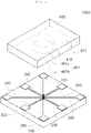
- FIGS. 1 and 2 are respectively an exploded perspective view and a cross-sectional view of an encapsulated structure for a quantum resistance standard according to an embodiment of the present invention.
- an encapsulated structure 1000 for the quantum resistance standard includes a base 100, an object 200, a conductive line 300, a cap 400, and an adhesive layer 500.
- the structure 1000 is used to measure a quantum Hall resistance under environment conditions of a temperature of about 1K and a magnetic field.
- the base 100 is a means supporting the object 200 providing a measurement value of the quantum Hall resistance and a plurality of conductive lines 300 connected to the object 200.
- the base 100 corresponds to a substrate formed of silicon carbide (SiC).
- the object 200 should be capable of providing the measurement value of the quantum Hall resistance by the quantum Hall effect in order to realize a quantum resistance standard.
- grapheme which may exhibit the quantum Hall effect in a measurement environment of the quantum Hall resistance with large and relaxed energy gap between Landau levels, that is, at a relatively high temperature and a low magnetic field compared to the existing measurement object.
- graphene is disposed on the base 100 as the object 200.
- the object 200 is epitaxial graphene grown on the base 100 which is a substrate formed of silicon carbide, and may be settled on the base 100 by being grown on the base 100 by sublimation of silicon atoms on a surface of silicon carbide in a certain environment.
- the plurality of conductive lines 300 are physically connected to the object in one end and electrically connected to a voltage measuring device or a current supplying device on the other end.
- the plurality of conductive lines 300 are metals having a very low resistance and aligned on the base 100.
- the plurality of conductive lines 300 includes at least two or more lines, and eight conductive lines 300 may be radially aligned on the base 100 as in the illustrated embodiment.
- the plurality of conductive lines 300 are formed of palladium (Pd) and gold (Au), where palladium is used as a contact metal directly connected to graphene. This is because when palladium and graphene are electrically connected to each other by contact, the resistance appears very low.
- the cap 400 serves as a protective film that isolates the object 200 from external air and blocks contact with external air, particularly, moisture or oxygen. Accordingly, a change in the quantum Hall resistance of the object 200 due to moisture or oxygen is prevented, and stability of the object 200 in the quantum Hall resistance measurement is maintained for a long time.
- the cap 400 includes a concave portion 410 recessed in a predetermined area 401a of one surface 401 and a flat area 401b excluding the predetermined area 401a on one surface where the concave portion is formed.
- the adhesive layer 500 is interposed between the flat area 401b and the base 100.
- the cap 400 is formed of glass. That is, the cap 400 is a glass cover.
- the adhesive layer 500 is formed of epoxy.
- the adhesive layer 500 is interposed so that penetration of oxygen or water molecules into a space including the inside of the concave portion 410 and the base on which the graphene is placed is blocked.
- the adhesive layer 500 is formed over the entire flat area 401b of the one surface 401 of the cap 400.
- the size of an area where the adhesive layer is formed, that is, the flat area 401b, may be formed as wide as possible in consideration of penetration possibility, the size of the base, and resistance according to lengths of the plurality of conductive lines.
- thermal stress may occur because thermal expansion coefficients of the cap, the base, and the adhesive layer formed of different materials are different from each other. This causes a crack through which water molecules or oxygen molecules may penetrate into the object 200.
- the thickness of the adhesive layer 500 is thickly formed by using a large amount of epoxy, cracks frequently occur during cooling. Accordingly, the adhesive layer 500 is formed to a thickness such that no crack occurs due to the temperature change by controlling the amount of epoxy.
- FIG. 3 is a flowchart of a method of manufacturing an encapsulated structure for a quantum resistance standard according to an embodiment of the present invention.
- the method of manufacturing the encapsulated structure for the quantum resistance standard includes steps of growing graphene on a base, forming a conductive line, and adhering a cap.
- graphene is used as an object for measuring a quantum Hall resistance due to the quantum Hall effect for realizing the quantum resistance standard.
- graphene is grown on a base formed of silicon carbide.
- Graphene is grown on the base heated to 1600°C under a gas pressure of 750 Torr argon by sublimation of silicon atoms on a surface of silicon carbide.
- the quality of the grown graphene was evaluated by atomic force microscopy (AFM) and scanning probe Raman spectroscopy.
- a plurality of conductive lines connected to the graphene are formed on the base to measure the quantum Hall resistance of the graphene.
- One end of the plurality of conductive lines is directly connected to the graphene, and the other end of the plurality of conductive lines is disposed near corners of the base.
- the plurality of conductive lines extend from one end to the other end, and are formed of palladium (Pd) and gold (Au).
- a structure in which the graphene and the plurality of radially extending conductive lines are formed on the base is annealed in a vacuum furnace at 500° C for about 30 minutes. Through an annealing step, organic residues present in the structure are removed while the structure is manufactured, and the graphene exhibits a quantum Hall phenomenon in a lower magnetic field.
- a cap for isolating the graphene from external air is adhered to the base.
- the cap is a cover formed of glass, a concave portion is formed to accommodate the graphene in a lower surface, and an area of the lower surface is flat except for an area where the concave portion is formed.
- an adhesive layer is interposed between the flat area of the lower surface of the cap and an upper surface of the base.
- the adhesive layer is formed as, for example, an epoxy adhesive.
- the measurement stability of the encapsulated structure is evaluated by exposing the encapsulated structure to air with a relative humidity of 90% for 24 hours. It was confirmed that the encapsulated structure hardly changed its electrical properties despite exposure to high humidity.
- a quantum Hall resistance value provided by graphene in a magnetic field equal to or greater than 8T was the same before and after exposure to humidity within a measurement uncertainty of about 3 ⁇ 10 -9 .
Landscapes
- Physics & Mathematics (AREA)
- General Physics & Mathematics (AREA)
- Condensed Matter Physics & Semiconductors (AREA)
- Engineering & Computer Science (AREA)
- Manufacturing & Machinery (AREA)
- Hall/Mr Elements (AREA)
Abstract
An encapsulated structure (1000) for a quantum resistance standard according to an embodiment of the present invention includes a base (100); an object (200) disposed on the base and providing a measurement value of the quantum Hall resistance; two or more conductive lines (300) connected to the object on one end; and a cap (400) isolating the object from outside air.
Description
- The present invention relates to an encapsulated structure for a quantum resistance standard, and more particularly, to an encapsulated structure for a quantum resistance standard having a long-term measurement stability by encapsulating a measurement object of a quantum Hall resistance.
- The quantum Hall effect is a phenomenon in which a Hall resistance has a certain value independent of a material under a specific condition and in which basic physical constant values of electron charge (e) and Planck's constant (h) appear as macroscopic measurement values that are called voltage.
- In the normal Hall effect where electric field (E) is generated in a direction perpendicular to current (i) and magnetic field, a Hall conductivity i/E changes in inverse proportion to the magnetic field. In this regard, when a semiconductor device capable of confining electrons in a two-dimensional surface flows a current (i) to a sample surface at a temperature equal to or lower than 1K and applies a magnetic field perpendicular to a direction of the current, a flat stairs shape is obtained where the Hall conductivity is an integer multiple of

- The quantum Hall effect is related to the fact that if a bunch of electrons quantized to the Landau level by the magnetic field is concentrated in one place due to impurities in a semiconductor, the electrons may not contribute to the current.
- The quantum Hall effect plays a key role in realizing the resistance standard by using a fixed value of a basic constant in the new International System of Units (SI) scheme that came into force in 2019.
- Many metrology institutions realize a quantum ohm based on the quantum Hall resistance (QHR) of

- In contrast, graphene exhibits the quantum Hall effect at a relatively high temperature and low magnetic field because the graphene has a large energy gap between Landau levels. It is useful to measure the quantized Hall resistance of graphene under relaxed experimental conditions, but there is a problem in that when the graphene is exposed to air, the graphene comes into contact with moisture, oxygen, and carbon impurities, and the quantum Hall resistance changes, making it impossible to use as the standard resistance.
- An object of the present invention is to provide an encapsulated structure capable of maintaining stability of a measurement object for a long time in measurement of a quantum Hall resistance for realization of a quantum resistance standard.
- In one general aspect, an encapsulated structure for a quantum resistance standard includes a base;an object disposed on the base and providing a measurement value of the quantum Hall resistance;two or more conductive lines connected to the object on one end; and a cap isolating the object from outside air.
- The object may include graphene.
- The graphene may correspond to epitaxial graphene grown on the base.
- The cap may include a concave portion recessed in a certain area of one surface and a flat area of the one surface except for the certain area in which the concave portion is formed, and an adhesive layer may be interposed between the flat area and the base when the object is accommodated in the concave portion.
- The cap may be formed of glass.
- The adhesive layer may be formed of epoxy.
- The encapsulated structure for the quantum resistance standard according to the present invention maintains the quantum Hall resistance measurement value despite a thermal change between cryogenic and room temperatures according to the quantum Hall resistance measurement and the exposure environment of humidity of 90%, that is, has the same long-term stability within a measurement uncertainty of about 3 in a billion.
- The effects obtainable in the present invention are not limited to the above-mentioned effects, and other effects not mentioned may be clearly understood by those of ordinary skill in the art to which the present invention belongs from the following description.
-
-
FIG. 1 is an exploded perspective view of an encapsulated structure for a quantum resistance standard according to an embodiment of the present invention. -
FIG. 2 is a cross-sectional view of an encapsulated structure for a quantum resistance standard according to an embodiment of the present invention. -
FIG. 3 is a flowchart of a method of manufacturing an encapsulated structure for a quantum resistance standard according to an embodiment of the present invention. - Hereinafter, the present invention will be described in detail with reference to the accompanying drawings.
- The terms used in this specification are terms defined in consideration of the functions of the present invention, which may vary according to the intention or custom of the user or operator. Therefore, definitions of these terms should be made based on the description throughout this specification.
- In addition, the embodiments disclosed below do not limit the scope of the present invention, but are merely exemplary matters of the components presented in the claims of the present invention, and are included in the technical spirit throughout the specification of the present invention and embodiments that are included in the technical spirit throughout the specification of the present invention and that include substitutable components as equivalents in the components of the claims may be included in the scope of the present invention.
- In the embodiments disclosed below, the terms such as 'first', 'second', 'one surface', 'the other surface', etc. are used to distinguish one component from other components, and the componentsare not limited by the terms. Hereinafter, in describing the present invention, detailed descriptions of known technologies that may obscure the subject matter of the present invention will be omitted.
-
FIGS. 1 and2 are respectively an exploded perspective view and a cross-sectional view of an encapsulated structure for a quantum resistance standard according to an embodiment of the present invention. - Referring to
FIGS. 1 and2 , anencapsulated structure 1000 for the quantum resistance standard according to an embodiment of the present invention includes abase 100, anobject 200, aconductive line 300, acap 400, and anadhesive layer 500. Thestructure 1000 is used to measure a quantum Hall resistance under environment conditions of a temperature of about 1K and a magnetic field. - The
base 100 is a means supporting theobject 200 providing a measurement value of the quantum Hall resistance and a plurality ofconductive lines 300 connected to theobject 200. In an embodiment, when theobject 200 corresponds to graphene, thebase 100 corresponds to a substrate formed of silicon carbide (SiC). - The
object 200 should be capable of providing the measurement value of the quantum Hall resistance by the quantum Hall effect in order to realize a quantum resistance standard. As described above, in an embodiment, grapheme which may exhibit the quantum Hall effect in a measurement environment of the quantum Hall resistance with large and relaxed energy gap between Landau levels, that is, at a relatively high temperature and a low magnetic field compared to the existing measurement object. - In an embodiment, graphene is disposed on the
base 100 as theobject 200. In an example, theobject 200 is epitaxial graphene grown on thebase 100 which is a substrate formed of silicon carbide, and may be settled on thebase 100 by being grown on thebase 100 by sublimation of silicon atoms on a surface of silicon carbide in a certain environment. - The plurality of
conductive lines 300 are physically connected to the object in one end and electrically connected to a voltage measuring device or a current supplying device on the other end. The plurality ofconductive lines 300 are metals having a very low resistance and aligned on thebase 100. The plurality ofconductive lines 300 includes at least two or more lines, and eightconductive lines 300 may be radially aligned on thebase 100 as in the illustrated embodiment. - In an example, the plurality of
conductive lines 300 are formed of palladium (Pd) and gold (Au), where palladium is used as a contact metal directly connected to graphene. This is because when palladium and graphene are electrically connected to each other by contact, the resistance appears very low. - The
cap 400 serves as a protective film that isolates theobject 200 from external air and blocks contact with external air, particularly, moisture or oxygen. Accordingly, a change in the quantum Hall resistance of theobject 200 due to moisture or oxygen is prevented, and stability of theobject 200 in the quantum Hall resistance measurement is maintained for a long time. - The
cap 400 includes aconcave portion 410 recessed in apredetermined area 401a of onesurface 401 and aflat area 401b excluding thepredetermined area 401a on one surface where the concave portion is formed. When thecap 400 is disposed on thebase 100 to accommodate theobject 200 in theconcave portion 410, theadhesive layer 500 is interposed between theflat area 401b and thebase 100. - In an embodiment, the
cap 400 is formed of glass. That is, thecap 400 is a glass cover. - In addition, in an embodiment, the
adhesive layer 500 is formed of epoxy. In the illustrated embodiment, when thecap 400 covers the graphene and is disposed on thebase 100, theadhesive layer 500 is interposed so that penetration of oxygen or water molecules into a space including the inside of theconcave portion 410 and the base on which the graphene is placed is blocked. - In order to completely block oxygen or water molecules, because even small holes through which oxygen or water molecules may enter and exit are not allowed, the
adhesive layer 500 is formed over the entireflat area 401b of the onesurface 401 of thecap 400. The size of an area where the adhesive layer is formed, that is, theflat area 401b, may be formed as wide as possible in consideration of penetration possibility, the size of the base, and resistance according to lengths of the plurality of conductive lines. - In addition, when the temperature falls to a cryogenic temperature for measurement of the quantum Hall resistance, thermal stress may occur because thermal expansion coefficients of the cap, the base, and the adhesive layer formed of different materials are different from each other. This causes a crack through which water molecules or oxygen molecules may penetrate into the
object 200. When the thickness of theadhesive layer 500 is thickly formed by using a large amount of epoxy, cracks frequently occur during cooling. Accordingly, theadhesive layer 500 is formed to a thickness such that no crack occurs due to the temperature change by controlling the amount of epoxy. -
FIG. 3 is a flowchart of a method of manufacturing an encapsulated structure for a quantum resistance standard according to an embodiment of the present invention. - Referring to
FIG. 3 , the method of manufacturing the encapsulated structure for the quantum resistance standard according to an embodiment of the present invention includes steps of growing graphene on a base, forming a conductive line, and adhering a cap. - In an embodiment, graphene is used as an object for measuring a quantum Hall resistance due to the quantum Hall effect for realizing the quantum resistance standard. As the object for measuring the quantum Hall resistance, graphene is grown on a base formed of silicon carbide. Graphene is grown on the base heated to 1600°C under a gas pressure of 750 Torr argon by sublimation of silicon atoms on a surface of silicon carbide. The quality of the grown graphene was evaluated by atomic force microscopy (AFM) and scanning probe Raman spectroscopy.
- Next, a plurality of conductive lines connected to the graphene are formed on the base to measure the quantum Hall resistance of the graphene. One end of the plurality of conductive lines is directly connected to the graphene, and the other end of the plurality of conductive lines is disposed near corners of the base. The plurality of conductive lines extend from one end to the other end, and are formed of palladium (Pd) and gold (Au).
- A structure in which the graphene and the plurality of radially extending conductive lines are formed on the base is annealed in a vacuum furnace at 500° C for about 30 minutes. Through an annealing step, organic residues present in the structure are removed while the structure is manufactured, and the graphene exhibits a quantum Hall phenomenon in a lower magnetic field.
- Next, in order to prevent the graphene from being decomposed by oxygen or moisture, a cap for isolating the graphene from external air is adhered to the base. The cap is a cover formed of glass, a concave portion is formed to accommodate the graphene in a lower surface, and an area of the lower surface is flat except for an area where the concave portion is formed.
- When the graphene is accommodated in the concave portion of the cap, an adhesive layer is interposed between the flat area of the lower surface of the cap and an upper surface of the base. The adhesive layer is formed as, for example, an epoxy adhesive. By controlling an amount of epoxy when the cap is adhered to the base, a crack due to a thermal stress difference according to materials between the cap, the base, and the adhesive layer is prevented at a temperature change over 300°C for measurement of the quantum Hall resistance measurement. Crack prevention ensures long-term stability of measurement of the quantum Hall resistance of graphene.
- Finally, the measurement stability of the encapsulated structure is evaluated by exposing the encapsulated structure to air with a relative humidity of 90% for 24 hours. It was confirmed that the encapsulated structure hardly changed its electrical properties despite exposure to high humidity. A quantum Hall resistance value provided by graphene in a magnetic field equal to or greater than 8T was the same before and after exposure to humidity within a measurement uncertainty of about 3×10⁻⁹.
-
- 1000
- encapsulated structure for quantum resistance standard
- 100
- base
- 200
- object
- 300
- conductive line
- 400
- cap
- 500
- adhesive layer
Claims (6)
- An encapsulated structure for a quantum resistance standard comprising:a base;an object disposed on the base and providing a measurement value of the quantum Hall resistance;two or more conductive lines connected to the object on one end; anda cap isolating the object from outside air.
- The encapsulated structure for the quantum resistance standard of claim 1,
wherein the object includes graphene. - The encapsulated structure for the quantum resistance standard of claim 2,
wherein the graphene corresponds to epitaxial graphene grown on the base. - The encapsulated structure for the quantum resistance standard of claim 1,wherein the cap includes a concave portion recessed in a certain area of one surface and a flat area of the one surface except for the certain area in which the concave portion is formed, andan adhesive layer is interposed between the flat area and the base when the object is accommodated in the concave portion.
- The encapsulated structure for the quantum resistance standard of claim 4,
wherein the cap is formed of glass. - The encapsulated structure for the quantum resistance standard of claim 4,
wherein the adhesive layer is formed of epoxy.
Applications Claiming Priority (1)
| Application Number | Priority Date | Filing Date | Title |
|---|---|---|---|
| KR1020210019796A KR102263568B1 (en) | 2021-02-15 | 2021-02-15 | Encapsulated constructure for quantum resistance standard |
Publications (1)
| Publication Number | Publication Date |
|---|---|
| EP4047381A1 true EP4047381A1 (en) | 2022-08-24 |
Family
ID=76376355
Family Applications (1)
| Application Number | Title | Priority Date | Filing Date |
|---|---|---|---|
| EP22156496.6A Withdrawn EP4047381A1 (en) | 2021-02-15 | 2022-02-14 | Encapsulated structure for quantum resistance standard |
Country Status (3)
| Country | Link |
|---|---|
| US (1) | US20220263015A1 (en) |
| EP (1) | EP4047381A1 (en) |
| KR (1) | KR102263568B1 (en) |
Families Citing this family (2)
| Publication number | Priority date | Publication date | Assignee | Title |
|---|---|---|---|---|
| CN115792381B (en) * | 2022-11-24 | 2023-06-23 | 中国计量科学研究院 | Device and method for precise measurement of load factor using combined quantum Hall resistance |
| EP4589308A1 (en) * | 2024-01-16 | 2025-07-23 | Physikalisch-Technische Bundesanstalt Braunschweig und Berlin | Measuring device for measuring an electrical resistance |
Citations (4)
| Publication number | Priority date | Publication date | Assignee | Title |
|---|---|---|---|---|
| US20130050227A1 (en) * | 2011-08-30 | 2013-02-28 | Qualcomm Mems Technologies, Inc. | Glass as a substrate material and a final package for mems and ic devices |
| US20150102807A1 (en) * | 2013-10-16 | 2015-04-16 | Infineon Technologies Ag | Hall effect sensor with graphene detection layer |
| US20200028031A1 (en) * | 2018-07-23 | 2020-01-23 | Shin-Etsu Chemical Co., Ltd. | Synthetic quartz glass cavity member, synthetic quartz glass cavity lid, optical device package, and making methods |
| WO2020180977A1 (en) * | 2019-03-04 | 2020-09-10 | University Of Maryland, College Park | Systems, devices, and methods for resistance metrology using graphene with superconducting components |
Family Cites Families (9)
| Publication number | Priority date | Publication date | Assignee | Title |
|---|---|---|---|---|
| DE4012081A1 (en) * | 1990-04-14 | 1991-10-17 | Bosch Gmbh Robert | METHOD AND ARRANGEMENT FOR MEASURING AIR AMOUNTS |
| US7127949B2 (en) * | 2003-07-08 | 2006-10-31 | National University Of Singapore | Contact pressure sensor and method for manufacturing the same |
| JP4496918B2 (en) * | 2004-10-26 | 2010-07-07 | 株式会社デンソー | Semiconductor device |
| DE102008047964A1 (en) * | 2008-09-18 | 2010-03-25 | Tesa Se | Method for encapsulating an electronic device |
| DE112011102705A5 (en) * | 2010-08-13 | 2013-05-29 | Tesa Se | Method for encapsulating an electronic device |
| KR20150116209A (en) * | 2014-04-07 | 2015-10-15 | 주식회사 이노칩테크놀로지 | Senser device |
| US10900927B2 (en) * | 2018-03-21 | 2021-01-26 | University Of South Carolina | Graphene field effect transistors for detection of ions |
| KR102214491B1 (en) * | 2019-08-13 | 2021-02-08 | 민남기 | Strain gauge chip and manufacturing method thereof, strain gauge sensor including the strain gauge chip and method of manufacturing the same |
| CN114200373B (en) * | 2021-12-09 | 2022-12-09 | 中国科学院上海微系统与信息技术研究所 | Small quantum resistance standard |
-
2021
- 2021-02-15 KR KR1020210019796A patent/KR102263568B1/en active Active
-
2022
- 2022-02-14 EP EP22156496.6A patent/EP4047381A1/en not_active Withdrawn
- 2022-02-14 US US17/670,781 patent/US20220263015A1/en not_active Abandoned
Patent Citations (4)
| Publication number | Priority date | Publication date | Assignee | Title |
|---|---|---|---|---|
| US20130050227A1 (en) * | 2011-08-30 | 2013-02-28 | Qualcomm Mems Technologies, Inc. | Glass as a substrate material and a final package for mems and ic devices |
| US20150102807A1 (en) * | 2013-10-16 | 2015-04-16 | Infineon Technologies Ag | Hall effect sensor with graphene detection layer |
| US20200028031A1 (en) * | 2018-07-23 | 2020-01-23 | Shin-Etsu Chemical Co., Ltd. | Synthetic quartz glass cavity member, synthetic quartz glass cavity lid, optical device package, and making methods |
| WO2020180977A1 (en) * | 2019-03-04 | 2020-09-10 | University Of Maryland, College Park | Systems, devices, and methods for resistance metrology using graphene with superconducting components |
Non-Patent Citations (2)
| Title |
|---|
| HANS HE ET AL: "Polymer-encapsulated molecular doped epigraphene for quantum resistance metrology", METROLOGIA, INSTITUTE OF PHYSICS PUBLISHING, BRISTOL, GB, vol. 56, no. 4, 28 June 2019 (2019-06-28), pages 45004, XP020341631, ISSN: 0026-1394, [retrieved on 20190628], DOI: 10.1088/1681-7575/AB2807 * |
| JARRETT DEAN G ET AL: "Transport of NIST Graphene Quantized Hall Devices and Comparison with AIST Gallium-Arsenide Quantized Hall Devices", 2018 CONFERENCE ON PRECISION ELECTROMAGNETIC MEASUREMENTS (CPEM 2018), IEEE, 8 July 2018 (2018-07-08), pages 1 - 2, XP033424385, DOI: 10.1109/CPEM.2018.8501079 * |
Also Published As
| Publication number | Publication date |
|---|---|
| KR102263568B1 (en) | 2021-06-11 |
| US20220263015A1 (en) | 2022-08-18 |
Similar Documents
| Publication | Publication Date | Title |
|---|---|---|
| JP4754995B2 (en) | Thermally conductive material and method for producing the same | |
| KR101341471B1 (en) | One hundred millimeter high purity semi-insulating single crystal silicon carbide wafer | |
| US20220263015A1 (en) | Encapsulated constructure for quantum resistance standard | |
| Yang et al. | Low carrier density epitaxial graphene devices on SiC | |
| Radermacher et al. | Optical and electrical properties of buried semiconducting ß-FeSL | |
| CN101521146B (en) | Substrate heating apparatus, semiconductor device manufacturing method, and semiconductor device | |
| Haque et al. | On-chip deposition of carbon nanotubes using CMOS microhotplates | |
| US6917021B2 (en) | Heating apparatus with electrostatic attraction function | |
| JP4523733B2 (en) | Method for producing silicon carbide single crystal ingot and method for mounting seed crystal for growing silicon carbide single crystal | |
| Elzinga et al. | Thermal transport properties of Sb Cl 5 graphite | |
| Haque et al. | Stability of electron field emission in Q-carbon | |
| EP2458355A2 (en) | Method of measuring the temperature of a sample carrier in a charged particle-optical apparatus | |
| CN119488009A (en) | Thermally stable graphene-containing laminates | |
| Li et al. | Measurement of the substitutional nitrogen activation energy in diamond films | |
| Anthopoulos et al. | Junction properties of nickel phthalocyanine thin sandwich film structures using dissimilar electrodes | |
| Koslowski et al. | Are protons involved in the hydrogen-induced surface conductivity of diamond (001)? | |
| US4140989A (en) | Temperature sensors | |
| Kopecek et al. | Structural and electrical properties of silicon epitaxial layers grown by LPE on highly resistive monocrystalline substrates | |
| Kalkan et al. | Epitaxial graphene thermistor for cryogenic temperatures | |
| Avigal et al. | The nature of ion-implanted contacts to polycrystalline diamond films | |
| US20090294776A1 (en) | Highly Oxygen-Sensitive Silicon Layer and Method for Obtaining Same | |
| CA2726986C (en) | Annealing of semi-insulating cdznte crystals | |
| CN116686429A (en) | Graphene Hall sensor and its manufacture and use | |
| Faggio et al. | Structural characterisation of ionising-radiation detectors based on CVD diamond films | |
| Foresi et al. | Piezoresistance and Quantum Confinement in Microcrystalline Silicon |
Legal Events
| Date | Code | Title | Description |
|---|---|---|---|
| PUAI | Public reference made under article 153(3) epc to a published international application that has entered the european phase |
Free format text: ORIGINAL CODE: 0009012 |
|
| STAA | Information on the status of an ep patent application or granted ep patent |
Free format text: STATUS: REQUEST FOR EXAMINATION WAS MADE |
|
| 17P | Request for examination filed |
Effective date: 20220214 |
|
| AK | Designated contracting states |
Kind code of ref document: A1 Designated state(s): AL AT BE BG CH CY CZ DE DK EE ES FI FR GB GR HR HU IE IS IT LI LT LU LV MC MK MT NL NO PL PT RO RS SE SI SK SM TR |
|
| STAA | Information on the status of an ep patent application or granted ep patent |
Free format text: STATUS: THE APPLICATION IS DEEMED TO BE WITHDRAWN |
|
| 18D | Application deemed to be withdrawn |
Effective date: 20230225 |