EP4047377A1 - Current detection apparatus, current detection method, current control apparatus, and current control method - Google Patents
Current detection apparatus, current detection method, current control apparatus, and current control method Download PDFInfo
- Publication number
- EP4047377A1 EP4047377A1 EP22156087.3A EP22156087A EP4047377A1 EP 4047377 A1 EP4047377 A1 EP 4047377A1 EP 22156087 A EP22156087 A EP 22156087A EP 4047377 A1 EP4047377 A1 EP 4047377A1
- Authority
- EP
- European Patent Office
- Prior art keywords
- current
- current detection
- current value
- distribution
- probability distribution
- Prior art date
- Legal status (The legal status is an assumption and is not a legal conclusion. Google has not performed a legal analysis and makes no representation as to the accuracy of the status listed.)
- Granted
Links
Images


Classifications
-
- G—PHYSICS
- G01—MEASURING; TESTING
- G01R—MEASURING ELECTRIC VARIABLES; MEASURING MAGNETIC VARIABLES
- G01R19/00—Arrangements for measuring currents or voltages or for indicating presence or sign thereof
- G01R19/0092—Measuring current only
-
- G—PHYSICS
- G01—MEASURING; TESTING
- G01R—MEASURING ELECTRIC VARIABLES; MEASURING MAGNETIC VARIABLES
- G01R15/00—Details of measuring arrangements of the types provided for in groups G01R17/00 - G01R29/00, G01R33/00 - G01R33/26 or G01R35/00
- G01R15/14—Adaptations providing voltage or current isolation, e.g. for high-voltage or high-current networks
- G01R15/146—Measuring arrangements for current not covered by other subgroups of G01R15/14, e.g. using current dividers, shunts, or measuring a voltage drop
-
- G—PHYSICS
- G01—MEASURING; TESTING
- G01R—MEASURING ELECTRIC VARIABLES; MEASURING MAGNETIC VARIABLES
- G01R15/00—Details of measuring arrangements of the types provided for in groups G01R17/00 - G01R29/00, G01R33/00 - G01R33/26 or G01R35/00
- G01R15/14—Adaptations providing voltage or current isolation, e.g. for high-voltage or high-current networks
- G01R15/20—Adaptations providing voltage or current isolation, e.g. for high-voltage or high-current networks using galvano-magnetic devices, e.g. Hall-effect devices, i.e. measuring a magnetic field via the interaction between a current and a magnetic field, e.g. magneto resistive or Hall effect devices
- G01R15/202—Adaptations providing voltage or current isolation, e.g. for high-voltage or high-current networks using galvano-magnetic devices, e.g. Hall-effect devices, i.e. measuring a magnetic field via the interaction between a current and a magnetic field, e.g. magneto resistive or Hall effect devices using Hall-effect devices
-
- G—PHYSICS
- G01—MEASURING; TESTING
- G01R—MEASURING ELECTRIC VARIABLES; MEASURING MAGNETIC VARIABLES
- G01R19/00—Arrangements for measuring currents or voltages or for indicating presence or sign thereof
- G01R19/25—Arrangements for measuring currents or voltages or for indicating presence or sign thereof using digital measurement techniques
- G01R19/2506—Arrangements for conditioning or analysing measured signals, e.g. for indicating peak values ; Details concerning sampling, digitizing or waveform capturing
-
- G—PHYSICS
- G05—CONTROLLING; REGULATING
- G05F—SYSTEMS FOR REGULATING ELECTRIC OR MAGNETIC VARIABLES
- G05F1/00—Automatic systems in which deviations of an electric quantity from one or more predetermined values are detected at the output of the system and fed back to a device within the system to restore the detected quantity to its predetermined value or values, i.e. retroactive systems
- G05F1/10—Regulating voltage or current
- G05F1/625—Regulating voltage or current wherein it is irrelevant whether the variable actually regulated is AC or DC
-
- G—PHYSICS
- G06—COMPUTING OR CALCULATING; COUNTING
- G06N—COMPUTING ARRANGEMENTS BASED ON SPECIFIC COMPUTATIONAL MODELS
- G06N7/00—Computing arrangements based on specific mathematical models
- G06N7/01—Probabilistic graphical models, e.g. probabilistic networks
-
- G—PHYSICS
- G01—MEASURING; TESTING
- G01R—MEASURING ELECTRIC VARIABLES; MEASURING MAGNETIC VARIABLES
- G01R1/00—Details of instruments or arrangements of the types included in groups G01R5/00 - G01R13/00 and G01R31/00
- G01R1/20—Modifications of basic electric elements for use in electric measuring instruments; Structural combinations of such elements with such instruments
- G01R1/203—Resistors used for electric measuring, e.g. decade resistors standards, resistors for comparators, series resistors, shunts
Definitions
- the disclosed embodiments relate to a current detection apparatus, a current detection method, a current control apparatus, and a current control method.
- a current detection apparatus that detects a current using a shunt resistor and a current detection apparatus that detects a current using a Hall element are known.
- a current control apparatus that controls an output current by using a current detected by the current detection apparatus as a feedback value is also known.
- Japanese Patent Application Laid-Open No. 2009-281774 shows a current detection apparatus including both the shunt resistor and the Hall element has also been proposed.
- a current detection apparatus includes a first current detection unit configured to detect a current flowing through a conductive wire with a shunt resistor connected to the conductive wire to obtain a first detected current value; a second current detection unit configured to detect the current with a Hall element to obtain a second detected current value; a storage unit configured to store a first probability distribution information indicating uncertainty of a detected current value detected by the first current detection unit and a second probability distribution information indicating uncertainty of a detected current value detected by the second current detection unit; a synthesis unit configured to convert the first detected current value into a first probability distribution based on the first probability distribution information, to convert the second detected current value into a second probability distribution based on the second probability distribution information, and to synthesize the first probability distribution and the second probability distribution to obtain a synthesized distribution; and an estimation unit configured to obtain an estimated current value via a maximum likelihood estimation based on the synthesized distribution.
- a current detection method includes detecting a current flowing through a conductive wire with a shunt resistor connected to the conductive wire to obtain a first detected current value, detecting the current with a Hall element to obtain a second detected current value, storing a first probability distribution information indicating uncertainty of a detected current value detected with the shunt resistor and a second probability distribution information indicating uncertainty of a detected current value detected with the Hall element, converting the first detected current value into a first probability distribution based on the first probability distribution information, converting the second detected current value into a second probability distribution based on the second probability distribution information, synthesizing the first probability distribution and the second probability distribution to obtain a synthesized distribution, and obtaining an estimated current value via a maximum likelihood estimation based on the synthesized distribution.
- the first detected current value regarding the shunt resistor and the second detected current value regarding the Hall element are handled as probability distributions, and the current value is estimated from the synthesized distribution obtained by synthesizing both distributions. That is, since the maximum likelihood (estimation of the most likely current value) in the current axis direction is performed on the probability distribution, the accuracy of current detection can be improved.
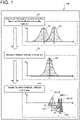
- FIG. 1 is a schematic diagram illustrating an overview of a current detection apparatus according to an embodiment. A specific configuration of the current detection apparatus will be described later with reference to FIGS. 2 and 3 .
- the current detection apparatus respectively detects a current flowing through a conductive wire to be targeted for detection by a first element and a second element having different characteristics.
- the first element is, for example, a shunt resistor
- the second element is, for example, a Hall element.
- the shunt resistor measures a voltage difference between both ends of the resistor and detects a current in accordance with Ohm's law, but has a defect that an output is multiplied by noise due to an ambient temperature or self-heating.
- the Hall element measures a magnetomotive force generated around an electric current and detects the electric current in a non-contact manner according to Ampere's law, but has a drawback that an output is multiplied by surrounding electromagnetic noise.
- the shunt resistor and the Hall element have the above-described disadvantages, when each of them is used alone, it cannot be said that the current detection accuracy is sufficiently high, and there is room for improvement from the viewpoint of the detection accuracy.
- the current flowing through the conductive wire is detected by the first element and the second element having different characteristics, and the detected value is treated as the probability distribution D. Then, the maximum likelihood estimation of the current is performed based on the synthesized distribution obtained by synthesizing the probability distributions.
- the first element and the second element it is preferable to use a combination of elements having different causes of accuracy deterioration, such as a combination of a shunt resistor and a Hall element.
- a combination of elements having different causes of accuracy deterioration such as a combination of a shunt resistor and a Hall element.
- the above-described "probability distribution” corresponds to a statistical distribution in which a current value measured via each element is an average ( ⁇ ) and a normal distribution having a variation of a standard deviation ( ⁇ ) is set. That is, it can be said that the probability distribution indicates the uncertainty of each of the detected values by each element.
- the standard deviation ( ⁇ ) of the current value measured via each element can be obtained from a catalog value of each element or can be obtained based on an experiment.
- the probability distribution may be referred to as a "probability distribution function".
- the maximum likelihood estimation of the current is performed based on an updated distribution obtained by Bayesian updating of the current synthesized distribution with the past synthesized distribution.
- the current detection apparatus regards each of the detected values of the current by the first element and the second element as probability distributions D (step S1). To be more specific, it is assumed that the current value detected by the first element is "i1" as indicated by a broken line frame in "step S1". In this case, the current detection apparatus treats the detected value by the first element as a "probability distribution D1" in which the i1 is an average ( ⁇ )and a standard deviation ( ⁇ ) corresponding to the first element.
- the current detection apparatus 100 treats the detected value by the second element as a "probability distribution D2" in which the i2 is an average ( ⁇ ) and a standard deviation ( ⁇ ) corresponding to the second element.
- the detected values of the elements can be combined in a statistically valid form by treating the detected values as not simple values but as a probabilistic distribution representing the uncertainty of each of the detected values.
- the current detection apparatus 100 generates a synthesized distribution SD for the current axis (I-axis) (step S2).
- the probability distributions D1 indicated in the step S1 are synthesized with the probability distributions D2, that is, the probability distributions D1 and D2 are synthesized on the probability axes (P-axes) to generate the synthesized distribution SD.
- the average ( ⁇ ) of the synthesized distribution SD is defined as "i3".
- the current detection apparatus 100 may use "i3" as the output value.
- the current detection apparatus performs Bayesian update of the synthesized distribution SD on the time base (T-axis) (step S3).
- updated distributions MDs are sequentially generated by Bayesian updating of the current synthesized distribution SD with the past synthesized distribution SD.
- the current detection apparatus 100 outputs a current value which is an average ( ⁇ ) of the updated distribution MD which is a result of the Bayesian update.
- Bayesian Updating refers to a known method of increasing the accuracy of estimation by updating an estimated value in accordance with information when the information is updated at any time.
- Bayesian update may be referred to as sequential Bayesian estimation.
- the current time is exemplified as t0
- the previous time is exemplified as t1
- the time before last is exemplified as t2.
- the synthesized distribution MD in t2 is the synthesized distribution MD (t2)
- the synthesized distribution MD in t1 is the synthesized distribution MD (t1)
- the synthesized distribution MD in t0 is the synthesized distribution MD (t0).
- the output value in t2 is i (t2)
- the output value in t1 is i (t1)
- the output value in t0 is i (t0).
- step S3 the standard deviation ( ⁇ ) in each synthesized distribution MD decreases as the Bayesian update is repeated, that is, the spread of the normal distribution in the direction of the current axis (I-axis) decreases, so that the accuracy of current detection can be increased. In this way, by performing maximum likelihood in the direction of the time axis, it is possible to further increase the accuracy of current detection.
- FIG. 2 is a schematic diagram showing a configuration example of a circuit.
- a shunt resistor 30 is provided on a conductive wire 5 as a current detection target, and a Hall element 40 is provided so as to be in non-contact with the conductive wire 5.
- the shunt resistor 30 and the Hall element 40 are disposed close to each other. With this arrangement, the size of the current detection apparatus 100 can be reduced.
- the Hall element 40 is not necessarily disposed in the vicinity of the shunt resistor 30. That is, since both elements can acquire the same current value as long as they are provided along the conductive wire 5 to be targeted for detection, the shunt resistor 30 and the Hall element 40 may be apparently separated from each other.
- the Hall element 40 is an IC type Hall element 40 and can detect not only an alternating current but also a direct current.
- An isolation amplifier 31a, a first phase shifter (an example of "first phase shifting circuitry") 31b, and an AD converter 31c are provided in order from the upstream side on a first output line 31 which is an output line of the shunt resistor 30.
- the isolation amplifier 31a is an amplifier that electrically isolates analog input signals and output signals from each other, and amplifies a voltage difference between both ends of the shunt resistor 30.
- the first phase shifter 3 1b delays the phase of the output waveform of the isolation amplifier 41a by an arbitrary time in order to match the phase of the output waveform of the amplifier 31a of the second output line 41.
- the AD converter 31c converts analog input signals into digital output signals.
- the second output line 41 which is an output line of the Hall element 40, is provided with an amplifier 41a, a second phase shifter (an example of "second phase shifting circuitry") 41b, and an AD converter 41c in this order from the upstream side.
- the amplifier 41a amplifies an output value of the Hall element 40.
- the second phase shifter 41b delays the phase of the output of the amplifier 41a by an arbitrary time in order to match the phase of the output waveform of the isolation amplifier 31a of the first output line 31.
- the AD converter 41c converts analog input signals into digital output signals.
- the phase shifters are provided in both the first output line 31 corresponding to the shunt resistor 30 and the second output line 41 corresponding to the Hall element 40. Therefore, even if either the system of the shunt resistor 30 or the system of the Hall element 40 is phase-delayed, phase matching can be performed, so that the present invention can be applied to not only DC current detection but also AC current detection without any problem.
- the detection target is a direct current
- the phase shifter of one of the first output line 31 and the second output line 41 may be omitted.
- the first output line 31 and the second output line 41 merge on the downstream side, and a CPU (Central Processing Unit) 10 and a memory 20 are provided at the merging destination.
- the output value generated by the CPU10 is output to the outside.
- the CPU10 and the memory 20 correspond to a control unit 10 and a storage unit 20 in FIG. 3 described later, respectively.
- each of the first output line 31 and the second output line 41 does not include a noise filter. This is because, as described above, the current detection apparatus 100 performs maximum likelihood estimation of the output value by combining the probability distributions of the two systems, and thus it is possible to suppress the influence of noise. In this way, by omitting the noise filter, it is possible to reduce the cost and size of the current detection apparatus 100.
- FIG. 3 is a block diagram showing a configuration of the current detection apparatus 100.
- the first output line 31 and the second output line 41 shown in FIG. 2 are not shown.
- the current detection apparatus 100 includes a control unit 10, a storage unit 20, a shunt resistor 30, and a Hall element 40. Since the shunt resistor 30 and the Hall element 40 have already been described with reference to FIG. 2 , the description thereof is omitted here.
- the control unit 10 includes a first current detection unit (an example of "first current detection circuitry") 11, a second current detection unit (an example of “second current detection circuitry”) 12, a synthesis unit (an example of "synthesis circuitry") 13, an estimation unit (an example of “estimation circuitry”) 14, a prediction unit (an example of "prediction circuitry”) 15, and an output unit 16.
- the storage unit (an example of “storage”) 20 stores probability distribution information 21 and learning information 22.
- control unit 10 includes, for example, a computer having a central processing unit (CPU), a read only memory (ROM), a random access memory (RAM), a hard disk drive (HDD), an input/output port, and the like, and various circuits.
- CPU central processing unit
- ROM read only memory
- RAM random access memory
- HDD hard disk drive
- the CPU of the computer functions as the first current detection unit 11, the second current detection unit 12, the synthesis unit 13, the estimation unit 14, the prediction unit 15, and the output unit 16 of the control unit 10 by reading and executing a program stored in the ROM.
- At least one or all of the first current detection unit 11, the second current detection unit 12, the synthesis unit 13, the estimation unit 14, the prediction unit 15, and the output unit 16 of the control unit 10 may be configured by hardware such as an application specific integrated circuit (ASIC) or a field programmable gate array (FPGA).
- ASIC application specific integrated circuit
- FPGA field programmable gate array
- the storage unit 20 corresponds to, for example, a RAM or an HDD.
- the RAM or the HDD can store the probability distribution information 21 and the learning information 22.
- the control unit 10 may acquire the above-described programs and various types of information via another computer or portable recording medium connected via a wired or wireless network.
- the first current detecting unit 11 outputs the current value of the system of the shunt resistor 30 to the synthesis unit 13. Further, the second current detection unit 12 outputs the current value of the system of the Hall element 40 to the synthesis unit 13. Note that the shunt resistor 30 and the Hall element 40 may be in any positional relationship with each other as long as the shunt resistor 30 and the Hall element 40 are located on the conductive wire 5 as a current detection target.
- the synthesis unit 13 Based on the probability distribution information 21 of the storage unit 20, the synthesis unit 13 converts the current value of the system of the shunt resistor 30 into a probability distribution and converts the current value of the system of the Hall element 40 into a probability distribution. Then, the synthesis unit 13 generates a synthesized distribution by synthesizing the probability distributions, and outputs the generated synthesized distribution to the estimation unit 14. Note that more specific processing contents of the synthesis unit 13 will be described later using FIG. 4A and FIG. 4B .
- the estimation unit 14 performs maximum likelihood estimation of current based on the synthesized distribution obtained by the synthesis unit. Specifically, the estimation unit 14 generates a maximum likelihood distribution by combining the predicted distribution obtained by the prediction unit 15 and the synthesized distribution received from the synthesis unit 13. Then, the estimation unit 14 outputs the average ( ⁇ ) of the generated maximum likelihood distribution to the output unit 16 as an estimated current (an estimated current value), and stores the generated maximum likelihood distribution in the storage unit 20 as the learning information 22 in association with time information.
- the prediction unit 15 generates a predicted synthesized distribution obtained by predicting the current synthesized distribution based on the learning information 22, and outputs the generated predicted distribution to the estimation unit 14. More specific processing contents of the estimation unit 14 and the prediction unit 15 will be described later with reference to FIG. 5 . Further, the output unit 16 outputs the estimated current received from the estimation unit 14 to the outside.
- the probability distribution information 21 is information including a variance ( ⁇ ) of current values measured via the shunt resistor 30 and a variance ( ⁇ ) of current values measured via the Hall element 40.
- the probability distribution information 21 may be simply referred to as "probability distribution 21".
- the learning information 22 is information in which a maximum likelihood distribution generated in the past by the estimation unit 14 is associated with time. Note that the learning information 22 may be only information of the maximum likelihood distribution generated immediately before or may include information of a plurality of maximum likelihood distributions in time series.
- FIG. 4A and FIG. 4B are schematic diagrams 1 and 2 showing the processing contents of the synthesis unit 13.
- the synthesis unit 13 when the current value detected by the system of the shunt resistor 30 is i1, the synthesis unit 13 generates a probability distribution Ds which is a normal distribution in which i1 is an average ( ⁇ ) and a standard deviation ( ⁇ ) corresponding to the shunt resistor 30 in the probability distribution information 21.
- the synthesis unit 13 generates a probability distribution Dh that is a normal distribution in which the i2 is an average ( ⁇ ) and a standard deviation ( ⁇ ) corresponding to the Hall elements 40 in the probability distribution information 21 is a standard deviation.
- the synthesis unit 13 generates a synthesized distribution SD for the current axis (I-axis).
- the probability distributions Ds and Dh shown in the FIG. 4A are combined on the probability axis (P-axis) to generate the synthesized distribution SD.
- the synthesis unit 13 outputs the generated synthesized distribution SD to the estimation unit 14. 13, which is the average ( ⁇ ) of the synthesized distribution SD, may be used as the output value of the current detection apparatus 100.
- FIG. 5 is a schematic diagram illustrating processing contents of the estimation unit 14 and the prediction unit 15.
- the synthesized distribution SD illustrated in FIG. 5 is the current synthesized distribution SD received by the estimation unit 14 from the synthesis unit 13.
- the predicted distribution PD illustrated in FIG. 5 is the current predicted distribution PD received from the prediction unit 15.
- the estimation unit 14 generates the maximum likelihood distribution MD by synthesizing the synthesized distribution SD received from the synthesis unit 13 and the predicted distribution PD received from the prediction unit 15 with respect to the probability axis (P axis). Then, the estimation unit 14 stores the generated maximum likelihood distribution MD in the storage unit 20 as the learning information 22, and outputs im, which is the average ( ⁇ ) of the maximum likelihood distribution MD, to the output unit 16.
- the estimation unit 14 synthesizes the synthesized distribution SD corresponding to the current value and the predicted distribution PD corresponding to the current value prediction predicted from the past synthesized distribution SD, it is possible to obtain the most likely current value reflecting the variation history from the past.
- FIG. 6 is a flowchart illustrating a processing procedure executed by the current detection apparatus 100.
- the current detection apparatus 100 repeats the processing procedure illustrated in FIG. 6 at each sampling timing.
- the current detection apparatus 100 detects a current via the shunt resistor 30 (step S101) and converts a detected value into a probability distribution based on the probability distribution information 21 (step S102). Further, the current detection apparatus 100 detects a current via the Hall element 40 (step S103), and converts the detected value into a probability distribution based on the probability distribution information 21 (step S104). Note that step S101 to step S102 and step S103 to step S104 are executed in parallel.
- the synthesis unit 13 generates the current synthesized distribution by synthesizing the probability distributions of the step S102 and the step S104 (step S105).
- the prediction unit 15 generates a predicted distribution based on the learning information 22 (step S106).
- the estimation unit 14 generates a maximum likelihood distribution by synthesizing the current synthesized distribution in step S105 and the predicted distribution in step S106 (step S107).
- the estimation unit 14 stores the maximum likelihood distribution in the step S107 in the learning information 22 (step S108), and the output unit 16 outputs a current value based on the maximum likelihood distribution in the step S107 (step S 109), and ends the process.
- the current detection apparatus 100 detects a current by a combination of the shunt resistor and the Hall element.
- different combinations of detection elements may be used.
- FIG. 7 is a diagram showing an example of combination of detection elements.
- the combination illustrated in Example 1 of FIG. 7 is a combination corresponding to the current detection apparatus 100 described in FIGS. 2 to 6 .
- Example 1 is a case where the shunt resistor is used as the first detection element and the Hall element is used as the second detection element.
- current detection targets are an alternating current and a direct current.
- the performance such as responsiveness and accuracy is good.
- Example 2 is an example in which a "current transformer” is used instead of the Hall element of Example 1. That is, the shunt resistor is used as the first detection element, and the current transformer is used as the second detection element.
- the detection target is limited to alternating current, unlike the case of Example 1. The performances such as responsiveness and accuracy are good as in Example 1.
- Example 3 is an example in which a "current transformer" is used instead of the shunt resistor of Example 1. That is, the current transformer is used as the first detection element and the Hall element is used as the second detection element.
- the detection target is limited to alternating current as in the case of Example 2.
- the performance such as responsiveness and accuracy is inferior to those of Example 1 and Example 2 because both elements are of a type affected by electromagnetic noise.
- a current control apparatus 200 including the current detection apparatus 100 described above may be configured.
- a current control apparatus 200 including the current detection apparatus 100 will be described below with reference to FIGS. 8 and 9.
- FIG. 8 is a block diagram showing a configuration of the current control apparatus 200
- FIG. 9 is a flowchart showing a processing procedure executed by the current control apparatus 200.
- the current control apparatus 200 includes the current detection apparatus 100 and an output control unit 210. Since the configuration of the current detection apparatus 100 has been described with reference to FIG. 3 and the like, the description thereof is omitted here.
- the output control unit 210 controls the output current based on the current output from the current detection apparatus 100.
- the output control unit 210 uses the current value detected by the current detection apparatus 100 as a feedback value to perform control for bringing the output current close to the target current.
- the output control unit 210 performs PI (proportional integral) control.
- P (proportional) control or PID (proportional-integral-derivative) control may be performed instead of the PI control.
- FIG. 8 illustrates a case where one current detection apparatus is provided, the current control apparatus 200 may include a plurality of current detection apparatuses 100.
- the current control apparatus 200 executes the processing procedure of the current detection apparatus 100 (see step S101 to step S109 in FIG. 6 ) (step S201). Subsequently, the output control unit 210 performs output control using the output value of the current detection apparatus 100 as a feedback value (step S202), and ends the processing.
- the current detection apparatus 100 includes the first current detection unit 11, the second current detection unit 12, the storage unit 20, the synthesis unit 13, the estimation unit 14, and the output unit 16.
- the first current detection unit 11 detects a current flowing through the conductive wire 5 to be targeted for detection by the shunt resistor 30.
- the second current detection unit 12 detects a current by the Hall element 40.
- the storage unit 20 stores a probability distribution indicating uncertainty of each detected value detected by the first current detection unit 11 and the second current detection unit 12.
- the synthesis unit synthesizes probability distributions respectively corresponding to the detected values.
- the estimation unit 14 performs maximum likelihood estimation of current based on the synthesized distribution obtained by the synthesis unit 13.
- the output unit 16 outputs the current estimated by maximum likelihood method.
- the detected value by the shunt resistor 30 and the detected value by the Hall element 40 are handled as probability distributions, and the current value is estimated from the synthesized distribution obtained by synthesizing both distributions. That is, since the maximum likelihood (estimation of the most likely current value) in the current axis direction is performed on the probability distribution, the accuracy of current detection can be improved.
- the current control apparatus 200 includes the current detection apparatus 100 and the output control unit 210.
- the output control unit 210 controls the output current based on the current output from the current detection apparatus 100.
- the accuracy of the current control can be improved.
- the number of shunt resistors 30 or the number of Hall elements 40 are one.
- the current detection apparatus 100 or the current control apparatus 200 including a plurality of shunt resistors 30 or a plurality of Hall elements 40 may be configured.
- a component suffixed with a term such as "member”, “portion”, “part”, “element”, “body”, and “structure” is intended to mean that there is a single such component or a plurality of such components.
- ordinal terms such as “first” and “second” are merely used for distinguishing purposes and there is no other intention (such as to connote a particular order) in using ordinal terms.
- first element does not connote the existence of “second element”; otherwise, the mere use of "second element” does not connote the existence of "first element”.
- approximating language such as “approximately”, “about”, and “substantially” may be applied to modify any quantitative representation that could permissibly vary without a significant change in the final result obtained. All of the quantitative representations recited in the present application shall be construed to be modified by approximating language such as “approximately”, “about”, and “substantially”.
Landscapes
- Physics & Mathematics (AREA)
- General Physics & Mathematics (AREA)
- Engineering & Computer Science (AREA)
- Theoretical Computer Science (AREA)
- Mathematical Optimization (AREA)
- General Engineering & Computer Science (AREA)
- Data Mining & Analysis (AREA)
- Evolutionary Computation (AREA)
- Artificial Intelligence (AREA)
- Mathematical Analysis (AREA)
- Algebra (AREA)
- Pure & Applied Mathematics (AREA)
- Computing Systems (AREA)
- Computational Mathematics (AREA)
- Mathematical Physics (AREA)
- Software Systems (AREA)
- Probability & Statistics with Applications (AREA)
- Power Engineering (AREA)
- Electromagnetism (AREA)
- Radar, Positioning & Navigation (AREA)
- Automation & Control Theory (AREA)
- Measurement Of Current Or Voltage (AREA)
- Measuring Instrument Details And Bridges, And Automatic Balancing Devices (AREA)
Abstract
Description
- The disclosed embodiments relate to a current detection apparatus, a current detection method, a current control apparatus, and a current control method.
- Conventionally, a current detection apparatus that detects a current using a shunt resistor and a current detection apparatus that detects a current using a Hall element are known. A current control apparatus that controls an output current by using a current detected by the current detection apparatus as a feedback value is also known.
-
Japanese Patent Application Laid-Open No. 2009-281774 - According to a first aspect of the present invention, a current detection apparatus includes a first current detection unit configured to detect a current flowing through a conductive wire with a shunt resistor connected to the conductive wire to obtain a first detected current value; a second current detection unit configured to detect the current with a Hall element to obtain a second detected current value; a storage unit configured to store a first probability distribution information indicating uncertainty of a detected current value detected by the first current detection unit and a second probability distribution information indicating uncertainty of a detected current value detected by the second current detection unit; a synthesis unit configured to convert the first detected current value into a first probability distribution based on the first probability distribution information, to convert the second detected current value into a second probability distribution based on the second probability distribution information, and to synthesize the first probability distribution and the second probability distribution to obtain a synthesized distribution; and an estimation unit configured to obtain an estimated current value via a maximum likelihood estimation based on the synthesized distribution.
- According to a second aspect of the present invention, a current detection method includes detecting a current flowing through a conductive wire with a shunt resistor connected to the conductive wire to obtain a first detected current value, detecting the current with a Hall element to obtain a second detected current value, storing a first probability distribution information indicating uncertainty of a detected current value detected with the shunt resistor and a second probability distribution information indicating uncertainty of a detected current value detected with the Hall element, converting the first detected current value into a first probability distribution based on the first probability distribution information, converting the second detected current value into a second probability distribution based on the second probability distribution information, synthesizing the first probability distribution and the second probability distribution to obtain a synthesized distribution, and obtaining an estimated current value via a maximum likelihood estimation based on the synthesized distribution.
- According to the first and second aspects, the first detected current value regarding the shunt resistor and the second detected current value regarding the Hall element are handled as probability distributions, and the current value is estimated from the synthesized distribution obtained by synthesizing both distributions. That is, since the maximum likelihood (estimation of the most likely current value) in the current axis direction is performed on the probability distribution, the accuracy of current detection can be improved.
- A more complete appreciation of the present disclosure and many of the attendant advantages thereof will be readily obtained as the same becomes better understood by reference to the following detailed description when considered in connection with the accompanying drawings.
-
FIG. 1 is a schematic diagram illustrating an overview of a current detection apparatus according to an embodiment. -
FIG. 2 is a schematic diagram showing a configuration example of a circuit. -
FIG. 3 is a block diagram showing a configuration of the current detection apparatus. -
FIG. 4A is a diagram 1 illustrating processing contents of the synthesis unit. -
FIG. 4B is a second diagram schematically illustrating the processing contents of the synthesis unit. -
FIG. 5 is a schematic diagram showing processing contents of the estimation unit and the prediction unit. -
FIG. 6 is a flowchart showing a processing procedure executed by the current detection apparatus. -
FIG. 7 is a diagram showing an example of a combination of detection elements. -
FIG. 8 is a block diagram showing a configuration of the current control apparatus. -
FIG. 9 is a flowchart showing a processing procedure executed by the current control apparatus. - Hereinafter, embodiments of a current detection apparatus, a current detection method, a current control apparatus, and a current control method disclosed in the present application will be described in detail with reference to the accompanying drawings. Note that the present invention is not limited to the embodiments described below.
- First, a current detection apparatus according to an embodiment will be described with reference to
FIG. 1. FIG. 1 is a schematic diagram illustrating an overview of a current detection apparatus according to an embodiment. A specific configuration of the current detection apparatus will be described later with reference toFIGS. 2 and3 . - As shown in
FIG. 1 , the current detection apparatus respectively detects a current flowing through a conductive wire to be targeted for detection by a first element and a second element having different characteristics. The first element is, for example, a shunt resistor, and the second element is, for example, a Hall element. Note that the horizontal axis of each graph indicated by a broken line frame in each step (step S1, step S2, and step S3) inFIG. 1 represents current (I), and the vertical axis represents probability (P). - Here, the shunt resistor measures a voltage difference between both ends of the resistor and detects a current in accordance with Ohm's law, but has a defect that an output is multiplied by noise due to an ambient temperature or self-heating. The Hall element measures a magnetomotive force generated around an electric current and detects the electric current in a non-contact manner according to Ampere's law, but has a drawback that an output is multiplied by surrounding electromagnetic noise.
- As described above, since the shunt resistor and the Hall element have the above-described disadvantages, when each of them is used alone, it cannot be said that the current detection accuracy is sufficiently high, and there is room for improvement from the viewpoint of the detection accuracy.
- Therefore, in the current detection apparatus according to the embodiment, the current flowing through the conductive wire is detected by the first element and the second element having different characteristics, and the detected value is treated as the probability distribution D. Then, the maximum likelihood estimation of the current is performed based on the synthesized distribution obtained by synthesizing the probability distributions.
- Here, as the first element and the second element, it is preferable to use a combination of elements having different causes of accuracy deterioration, such as a combination of a shunt resistor and a Hall element. By using elements having different characteristics as described above, defects can be compensated for each other, and detection accuracy can be easily improved.
- In addition, the above-described "probability distribution" corresponds to a statistical distribution in which a current value measured via each element is an average (µ) and a normal distribution having a variation of a standard deviation (σ) is set. That is, it can be said that the probability distribution indicates the uncertainty of each of the detected values by each element. The standard deviation (σ) of the current value measured via each element can be obtained from a catalog value of each element or can be obtained based on an experiment. The probability distribution may be referred to as a "probability distribution function".
- Further, in the
current detection apparatus 100 according to the embodiment, in addition to the maximum likelihood estimation of the current based on the synthesized distribution, the maximum likelihood estimation of the current is performed based on an updated distribution obtained by Bayesian updating of the current synthesized distribution with the past synthesized distribution. - Hereinafter, the above-described processing contents will be specifically described. First, the current detection apparatus regards each of the detected values of the current by the first element and the second element as probability distributions D (step S1). To be more specific, it is assumed that the current value detected by the first element is "i1" as indicated by a broken line frame in "step S1". In this case, the current detection apparatus treats the detected value by the first element as a "probability distribution D1" in which the i1 is an average (µ)and a standard deviation (σ) corresponding to the first element.
- Similarly, it is assumed that the current value detected by the second element is "i2". In this case, the
current detection apparatus 100 treats the detected value by the second element as a "probability distribution D2" in which the i2 is an average (µ) and a standard deviation (σ) corresponding to the second element. In this way, the detected values of the elements can be combined in a statistically valid form by treating the detected values as not simple values but as a probabilistic distribution representing the uncertainty of each of the detected values. - Next, the
current detection apparatus 100 generates a synthesized distribution SD for the current axis (I-axis) (step S2). To be more specific, as indicated by broken line frame in "step S2", the probability distributions D1 indicated in the step S1 are synthesized with the probability distributions D2, that is, the probability distributions D1 and D2 are synthesized on the probability axes (P-axes) to generate the synthesized distribution SD. Here, the average (µ) of the synthesized distribution SD is defined as "i3". Thecurrent detection apparatus 100 may use "i3" as the output value. - Subsequently, the current detection apparatus performs Bayesian update of the synthesized distribution SD on the time base (T-axis) (step S3). To be specific, as indicated by a broken line frame in "Step S3", updated distributions MDs are sequentially generated by Bayesian updating of the current synthesized distribution SD with the past synthesized distribution SD. Then, the
current detection apparatus 100 outputs a current value which is an average (µ) of the updated distribution MD which is a result of the Bayesian update. - Here, Bayesian Updating refers to a known method of increasing the accuracy of estimation by updating an estimated value in accordance with information when the information is updated at any time. Bayesian update may be referred to as sequential Bayesian estimation.
- In the step S3, the current time is exemplified as t0, the previous time is exemplified as t1, and the time before last is exemplified as t2. Describing in time series, the synthesized distribution MD in t2 is the synthesized distribution MD (t2), the synthesized distribution MD in t1 is the synthesized distribution MD (t1), and the synthesized distribution MD in t0 is the synthesized distribution MD (t0). Further, the output value in t2 is i (t2), the output value in t1 is i (t1), and the output value in t0 is i (t0).
- As shown in step S3, the standard deviation (σ) in each synthesized distribution MD decreases as the Bayesian update is repeated, that is, the spread of the normal distribution in the direction of the current axis (I-axis) decreases, so that the accuracy of current detection can be increased. In this way, by performing maximum likelihood in the direction of the time axis, it is possible to further increase the accuracy of current detection.
- Next, an example of a circuit configuration of the
current detection apparatus 100 shown inFIG. 1 will be described with reference toFIG. 2. FIG. 2 is a schematic diagram showing a configuration example of a circuit. As shown inFIG. 2 , ashunt resistor 30 is provided on aconductive wire 5 as a current detection target, and aHall element 40 is provided so as to be in non-contact with theconductive wire 5. In the case shown inFIG. 2 , theshunt resistor 30 and theHall element 40 are disposed close to each other. With this arrangement, the size of thecurrent detection apparatus 100 can be reduced. - The
Hall element 40 is not necessarily disposed in the vicinity of theshunt resistor 30. That is, since both elements can acquire the same current value as long as they are provided along theconductive wire 5 to be targeted for detection, theshunt resistor 30 and theHall element 40 may be apparently separated from each other. Here, theHall element 40 is an ICtype Hall element 40 and can detect not only an alternating current but also a direct current. - An
isolation amplifier 31a, a first phase shifter (an example of "first phase shifting circuitry") 31b, and anAD converter 31c are provided in order from the upstream side on afirst output line 31 which is an output line of theshunt resistor 30. Theisolation amplifier 31a is an amplifier that electrically isolates analog input signals and output signals from each other, and amplifies a voltage difference between both ends of theshunt resistor 30. - The
first phase shifter 3 1b delays the phase of the output waveform of theisolation amplifier 41a by an arbitrary time in order to match the phase of the output waveform of theamplifier 31a of thesecond output line 41. TheAD converter 31c converts analog input signals into digital output signals. - The
second output line 41, which is an output line of theHall element 40, is provided with anamplifier 41a, a second phase shifter (an example of "second phase shifting circuitry") 41b, and anAD converter 41c in this order from the upstream side. Theamplifier 41a amplifies an output value of theHall element 40. Thesecond phase shifter 41b delays the phase of the output of theamplifier 41a by an arbitrary time in order to match the phase of the output waveform of theisolation amplifier 31a of thefirst output line 31. TheAD converter 41c converts analog input signals into digital output signals. - As described above, in the
current detection apparatus 100, the phase shifters are provided in both thefirst output line 31 corresponding to theshunt resistor 30 and thesecond output line 41 corresponding to theHall element 40. Therefore, even if either the system of theshunt resistor 30 or the system of theHall element 40 is phase-delayed, phase matching can be performed, so that the present invention can be applied to not only DC current detection but also AC current detection without any problem. When the detection target is a direct current, the phase shifter of one of thefirst output line 31 and thesecond output line 41 may be omitted. - Further, as shown in
FIG. 2 , thefirst output line 31 and thesecond output line 41 merge on the downstream side, and a CPU (Central Processing Unit) 10 and amemory 20 are provided at the merging destination. The output value generated by the CPU10 is output to the outside. The CPU10 and thememory 20 correspond to acontrol unit 10 and astorage unit 20 inFIG. 3 described later, respectively. - As shown in
FIG. 2 , each of thefirst output line 31 and thesecond output line 41 does not include a noise filter. This is because, as described above, thecurrent detection apparatus 100 performs maximum likelihood estimation of the output value by combining the probability distributions of the two systems, and thus it is possible to suppress the influence of noise. In this way, by omitting the noise filter, it is possible to reduce the cost and size of thecurrent detection apparatus 100. - Next, a configuration of the
current detection apparatus 100 will be described with reference toFIG. 3. FIG. 3 is a block diagram showing a configuration of thecurrent detection apparatus 100. InFIG. 3 , thefirst output line 31 and thesecond output line 41 shown inFIG. 2 are not shown. - As shown in
FIG. 3 , thecurrent detection apparatus 100 includes acontrol unit 10, astorage unit 20, ashunt resistor 30, and aHall element 40. Since theshunt resistor 30 and theHall element 40 have already been described with reference toFIG. 2 , the description thereof is omitted here. - The
control unit 10 includes a first current detection unit (an example of "first current detection circuitry") 11, a second current detection unit (an example of "second current detection circuitry") 12, a synthesis unit (an example of "synthesis circuitry") 13, an estimation unit (an example of "estimation circuitry") 14, a prediction unit (an example of "prediction circuitry") 15, and anoutput unit 16. The storage unit (an example of "storage") 20 storesprobability distribution information 21 and learninginformation 22. - Here, the
control unit 10 includes, for example, a computer having a central processing unit (CPU), a read only memory (ROM), a random access memory (RAM), a hard disk drive (HDD), an input/output port, and the like, and various circuits. - For example, the CPU of the computer functions as the first
current detection unit 11, the secondcurrent detection unit 12, thesynthesis unit 13, theestimation unit 14, theprediction unit 15, and theoutput unit 16 of thecontrol unit 10 by reading and executing a program stored in the ROM. - Further, at least one or all of the first
current detection unit 11, the secondcurrent detection unit 12, thesynthesis unit 13, theestimation unit 14, theprediction unit 15, and theoutput unit 16 of thecontrol unit 10 may be configured by hardware such as an application specific integrated circuit (ASIC) or a field programmable gate array (FPGA). - The
storage unit 20 corresponds to, for example, a RAM or an HDD. The RAM or the HDD can store theprobability distribution information 21 and the learninginformation 22. Note that thecontrol unit 10 may acquire the above-described programs and various types of information via another computer or portable recording medium connected via a wired or wireless network. - The first current detecting
unit 11 outputs the current value of the system of theshunt resistor 30 to thesynthesis unit 13. Further, the secondcurrent detection unit 12 outputs the current value of the system of theHall element 40 to thesynthesis unit 13. Note that theshunt resistor 30 and theHall element 40 may be in any positional relationship with each other as long as theshunt resistor 30 and theHall element 40 are located on theconductive wire 5 as a current detection target. - Based on the
probability distribution information 21 of thestorage unit 20, thesynthesis unit 13 converts the current value of the system of theshunt resistor 30 into a probability distribution and converts the current value of the system of theHall element 40 into a probability distribution. Then, thesynthesis unit 13 generates a synthesized distribution by synthesizing the probability distributions, and outputs the generated synthesized distribution to theestimation unit 14. Note that more specific processing contents of thesynthesis unit 13 will be described later usingFIG. 4A and FIG. 4B . - The
estimation unit 14 performs maximum likelihood estimation of current based on the synthesized distribution obtained by the synthesis unit. Specifically, theestimation unit 14 generates a maximum likelihood distribution by combining the predicted distribution obtained by theprediction unit 15 and the synthesized distribution received from thesynthesis unit 13. Then, theestimation unit 14 outputs the average (µ) of the generated maximum likelihood distribution to theoutput unit 16 as an estimated current (an estimated current value), and stores the generated maximum likelihood distribution in thestorage unit 20 as the learninginformation 22 in association with time information. - The
prediction unit 15 generates a predicted synthesized distribution obtained by predicting the current synthesized distribution based on the learninginformation 22, and outputs the generated predicted distribution to theestimation unit 14. More specific processing contents of theestimation unit 14 and theprediction unit 15 will be described later with reference toFIG. 5 . Further, theoutput unit 16 outputs the estimated current received from theestimation unit 14 to the outside. - The
probability distribution information 21 is information including a variance (σ) of current values measured via theshunt resistor 30 and a variance (σ) of current values measured via theHall element 40. Here, theprobability distribution information 21 may be simply referred to as "probability distribution 21". Further, the learninginformation 22 is information in which a maximum likelihood distribution generated in the past by theestimation unit 14 is associated with time. Note that the learninginformation 22 may be only information of the maximum likelihood distribution generated immediately before or may include information of a plurality of maximum likelihood distributions in time series. - Next, the processing contents of the
synthesis unit 13 shown inFIG. 3 will be described with reference toFIGS. 4A and 4B. FIG. 4A and FIG. 4B are schematic diagrams 1 and 2 showing the processing contents of thesynthesis unit 13. - As illustrated in
FIG. 4A , when the current value detected by the system of theshunt resistor 30 is i1, thesynthesis unit 13 generates a probability distribution Ds which is a normal distribution in which i1 is an average (µ) and a standard deviation (σ) corresponding to theshunt resistor 30 in theprobability distribution information 21. - In addition, in a case where the current detected by the system of the
Hall elements 40 is a i2, thesynthesis unit 13 generates a probability distribution Dh that is a normal distribution in which the i2 is an average (µ) and a standard deviation (σ) corresponding to theHall elements 40 in theprobability distribution information 21 is a standard deviation. - Subsequently, as illustrated in
FIG. 4B , thesynthesis unit 13 generates a synthesized distribution SD for the current axis (I-axis). To be specific, the probability distributions Ds and Dh shown in theFIG. 4A are combined on the probability axis (P-axis) to generate the synthesized distribution SD. Then, thesynthesis unit 13 outputs the generated synthesized distribution SD to theestimation unit 14. 13, which is the average (µ) of the synthesized distribution SD, may be used as the output value of thecurrent detection apparatus 100. - Next, processing contents of the
estimation unit 14 and theprediction unit 15 shown inFIG. 3 will be described with reference toFIG. 5. FIG. 5 is a schematic diagram illustrating processing contents of theestimation unit 14 and theprediction unit 15. The synthesized distribution SD illustrated inFIG. 5 is the current synthesized distribution SD received by theestimation unit 14 from thesynthesis unit 13. The predicted distribution PD illustrated inFIG. 5 is the current predicted distribution PD received from theprediction unit 15. - The
estimation unit 14 generates the maximum likelihood distribution MD by synthesizing the synthesized distribution SD received from thesynthesis unit 13 and the predicted distribution PD received from theprediction unit 15 with respect to the probability axis (P axis). Then, theestimation unit 14 stores the generated maximum likelihood distribution MD in thestorage unit 20 as the learninginformation 22, and outputs im, which is the average (µ) of the maximum likelihood distribution MD, to theoutput unit 16. - As described above, since the
estimation unit 14 synthesizes the synthesized distribution SD corresponding to the current value and the predicted distribution PD corresponding to the current value prediction predicted from the past synthesized distribution SD, it is possible to obtain the most likely current value reflecting the variation history from the past. - Next, a processing procedure executed by the
current detection apparatus 100 will be described with reference toFIG. 6. FIG. 6 is a flowchart illustrating a processing procedure executed by thecurrent detection apparatus 100. Thecurrent detection apparatus 100 repeats the processing procedure illustrated inFIG. 6 at each sampling timing. - As illustrated in
FIG. 6 , thecurrent detection apparatus 100 detects a current via the shunt resistor 30 (step S101) and converts a detected value into a probability distribution based on the probability distribution information 21 (step S102). Further, thecurrent detection apparatus 100 detects a current via the Hall element 40 (step S103), and converts the detected value into a probability distribution based on the probability distribution information 21 (step S104). Note that step S101 to step S102 and step S103 to step S104 are executed in parallel. - Subsequently, the
synthesis unit 13 generates the current synthesized distribution by synthesizing the probability distributions of the step S102 and the step S104 (step S105). Then, theprediction unit 15 generates a predicted distribution based on the learning information 22 (step S106). Further, theestimation unit 14 generates a maximum likelihood distribution by synthesizing the current synthesized distribution in step S105 and the predicted distribution in step S106 (step S107). - In addition, the
estimation unit 14 stores the maximum likelihood distribution in the step S107 in the learning information 22 (step S108), and theoutput unit 16 outputs a current value based on the maximum likelihood distribution in the step S107 (step S 109), and ends the process. - Although the case where the
current detection apparatus 100 detects a current by a combination of the shunt resistor and the Hall element has been described above, different combinations of detection elements may be used. - In the following, variations of combinations of detection elements will be described with reference to
FIG. 7. FIG. 7 is a diagram showing an example of combination of detection elements. The combination illustrated in Example 1 ofFIG. 7 is a combination corresponding to thecurrent detection apparatus 100 described inFIGS. 2 to 6 . - As shown in
FIG. 7 , "Example 1" is a case where the shunt resistor is used as the first detection element and the Hall element is used as the second detection element. In the case of the combination of Example 1, as described above, current detection targets are an alternating current and a direct current. In addition, the performance such as responsiveness and accuracy is good. - Example 2 is an example in which a "current transformer" is used instead of the Hall element of Example 1. That is, the shunt resistor is used as the first detection element, and the current transformer is used as the second detection element. In the case of the combination of Example 2, the detection target is limited to alternating current, unlike the case of Example 1. The performances such as responsiveness and accuracy are good as in Example 1.
- Example 3 is an example in which a "current transformer" is used instead of the shunt resistor of Example 1. That is, the current transformer is used as the first detection element and the Hall element is used as the second detection element. In the case of the combination of Example 3, the detection target is limited to alternating current as in the case of Example 2. In addition, the performance such as responsiveness and accuracy is inferior to those of Example 1 and Example 2 because both elements are of a type affected by electromagnetic noise.
- A
current control apparatus 200 including thecurrent detection apparatus 100 described above may be configured. Acurrent control apparatus 200 including thecurrent detection apparatus 100 will be described below with reference toFIGS. 8 and 9. FIG. 8 is a block diagram showing a configuration of thecurrent control apparatus 200, andFIG. 9 is a flowchart showing a processing procedure executed by thecurrent control apparatus 200. - As illustrated in
FIG. 8 , thecurrent control apparatus 200 includes thecurrent detection apparatus 100 and anoutput control unit 210. Since the configuration of thecurrent detection apparatus 100 has been described with reference toFIG. 3 and the like, the description thereof is omitted here. Theoutput control unit 210 controls the output current based on the current output from thecurrent detection apparatus 100. - For example, the
output control unit 210 uses the current value detected by thecurrent detection apparatus 100 as a feedback value to perform control for bringing the output current close to the target current. Here, it is assumed that theoutput control unit 210 performs PI (proportional integral) control. P (proportional) control or PID (proportional-integral-derivative) control may be performed instead of the PI control. - In this way, since the
current control apparatus 200 performs current control using the current detected by thecurrent detection apparatus 100 having high current detection accuracy, it is possible to increase the accuracy of current control. AlthoughFIG. 8 illustrates a case where one current detection apparatus is provided, thecurrent control apparatus 200 may include a plurality ofcurrent detection apparatuses 100. - As shown in
FIG. 9 , thecurrent control apparatus 200 executes the processing procedure of the current detection apparatus 100 (see step S101 to step S109 inFIG. 6 ) (step S201). Subsequently, theoutput control unit 210 performs output control using the output value of thecurrent detection apparatus 100 as a feedback value (step S202), and ends the processing. - As described above, the
current detection apparatus 100 according to the embodiment includes the firstcurrent detection unit 11, the secondcurrent detection unit 12, thestorage unit 20, thesynthesis unit 13, theestimation unit 14, and theoutput unit 16. The firstcurrent detection unit 11 detects a current flowing through theconductive wire 5 to be targeted for detection by theshunt resistor 30. The secondcurrent detection unit 12 detects a current by theHall element 40. Thestorage unit 20 stores a probability distribution indicating uncertainty of each detected value detected by the firstcurrent detection unit 11 and the secondcurrent detection unit 12. The synthesis unit synthesizes probability distributions respectively corresponding to the detected values. Theestimation unit 14 performs maximum likelihood estimation of current based on the synthesized distribution obtained by thesynthesis unit 13. Theoutput unit 16 outputs the current estimated by maximum likelihood method. - As described above, according to the
current detection apparatus 100 of the embodiment, the detected value by theshunt resistor 30 and the detected value by theHall element 40 are handled as probability distributions, and the current value is estimated from the synthesized distribution obtained by synthesizing both distributions. That is, since the maximum likelihood (estimation of the most likely current value) in the current axis direction is performed on the probability distribution, the accuracy of current detection can be improved. - The
current control apparatus 200 according to the embodiment includes thecurrent detection apparatus 100 and theoutput control unit 210. Theoutput control unit 210 controls the output current based on the current output from thecurrent detection apparatus 100. As described above, according to thecurrent control apparatus 200 of the embodiment, since the output current is controlled based on the current output from thecurrent detection apparatus 100, the accuracy of the current control can be improved. - In the above-described embodiment, the number of
shunt resistors 30 or the number ofHall elements 40 are one. However, thecurrent detection apparatus 100 or thecurrent control apparatus 200 including a plurality ofshunt resistors 30 or a plurality ofHall elements 40 may be configured. - Further effects and modifications can be easily derived by those skilled in the art. Therefore, the broader aspects of the present invention are not limited to the specific details and representative examples shown and described above. Accordingly, various modifications may be made without departing from the spirit or scope of the general inventive concept as defined by the appended claims and their equivalents.
- As used herein, the term "comprise" and its variations are intended to mean openended terms, not excluding any other elements and/or components that are not recited herein. The same applies to the terms "include", "have", and their variations.
- As used herein, a component suffixed with a term such as "member", "portion", "part", "element", "body", and "structure" is intended to mean that there is a single such component or a plurality of such components.
- As used herein, ordinal terms such as "first" and "second" are merely used for distinguishing purposes and there is no other intention (such as to connote a particular order) in using ordinal terms. For example, the mere use of "first element" does not connote the existence of "second element"; otherwise, the mere use of "second element" does not connote the existence of "first element".
- As used herein, approximating language such as "approximately", "about", and "substantially" may be applied to modify any quantitative representation that could permissibly vary without a significant change in the final result obtained. All of the quantitative representations recited in the present application shall be construed to be modified by approximating language such as "approximately", "about", and "substantially".
- As used herein, the phrase "at least one of A and B" is intended to be interpreted as "only A", "only B", or "both A and B".
- Obviously, numerous modifications and variations of the present disclosure are possible in light of the above teachings. It is therefore to be understood that within the scope of the appended claims, the present disclosure may be practiced otherwise than as specifically described herein.
Claims (10)
- A current detection apparatus (100) comprising:a first current detection unit (11) configured to detect a current flowing through a conductive wire (5) with a shunt resistor (30) connected to the conductive wire (5) to obtain a first detected current value;a second current detection unit (12) configured to detect the current with a Hall element (40) to obtain a second detected current value;a storage unit (20) configured to store a first probability distribution information indicating uncertainty of a detected current value detected by the first current detection unit (11) and a second probability distribution information indicating uncertainty of a detected current value detected by the second current detection unit (12);a synthesis unit (13) configured to convert the first detected current value into a first probability distribution based on the first probability distribution information, to convert the second detected current value into a second probability distribution based on the second probability distribution information, and to synthesize the first probability distribution and the second probability distribution to obtain a synthesized distribution (SD); andan estimation unit (14) configured to obtain an estimated current value via a maximum likelihood estimation based on the synthesized distribution (SD).
- The current detection apparatus (100) according to claim 1, wherein the estimation unit (14) is configured to obtain the estimated current value based on an updated synthesized distribution (SD) obtained by updating a current synthesized distribution (SD) with a past synthesized distribution (SD) via Bayesian updating.
- The current detection apparatus (100) according to claim 2, further comprising:a prediction unit (15) configured to predict a predicted distribution based on learning information (22), the storage unit (20) being configured to store the past synthesized distribution (SD) as the learning information (22),wherein the estimation unit (14) is configured to obtain the estimated current value by synthesizing the predicted distribution and the current synthesized distribution (SD).
- The current detection apparatus (100) according to any one of claims 1 to 3, further comprising:a first phase shifter (31b) provided on an output line of the shunt resistor (30); anda second phase shifter (41b) provided on an output line of the Hall element (40).
- The current detection apparatus (100) according to any one of claims 1 to 4,
wherein an output line of the shunt resistor (30) and an output line of the Hall element (40) do not have a noise filter. - The current detection apparatus (100) according to any one of claims 1 to 5, further comprising:
an output unit (16) configured to output the estimated current value. - A current detection method comprising:detecting a current flowing through a conductive wire (5) with a shunt resistor (30) connected to the conductive wire (5) to obtain a first detected current value;detecting the current with a Hall element (40) to obtain a second detected current value;storing a first probability distribution information indicating uncertainty of a detected current value detected with the shunt resistor (30) and a second probability distribution information indicating uncertainty of a detected current value detected with the Hall element (40);converting the first detected current value into a first probability distribution based on the first probability distribution information;converting the second detected current value into a second probability distribution based on the second probability distribution information;synthesizing the first probability distribution and the second probability distribution to obtain a synthesized distribution (SD); andobtaining an estimated current value via a maximum likelihood estimation based on the synthesized distribution (SD).
- A current control apparatus (200) comprising:
the current detection apparatus (100) according to any one of claims 1 to 6; and
an output control unit (210) configured to control an output current based on the estimated current value. - The current detection method according to claim 7, further comprising:
outputting the estimated current value. - A current control method comprising:the current detection method according to claim 7 or claim 9; andcontrolling an output current based on the estimated current value.
Applications Claiming Priority (1)
| Application Number | Priority Date | Filing Date | Title |
|---|---|---|---|
| JP2021026216A JP7173187B2 (en) | 2021-02-22 | 2021-02-22 | Current detection device, current detection method, current control device and current control method |
Publications (2)
| Publication Number | Publication Date |
|---|---|
| EP4047377A1 true EP4047377A1 (en) | 2022-08-24 |
| EP4047377B1 EP4047377B1 (en) | 2024-09-11 |
Family
ID=80446413
Family Applications (1)
| Application Number | Title | Priority Date | Filing Date |
|---|---|---|---|
| EP22156087.3A Active EP4047377B1 (en) | 2021-02-22 | 2022-02-10 | Current detection apparatus, current detection method, current control apparatus, and current control method |
Country Status (4)
| Country | Link |
|---|---|
| US (1) | US11846657B2 (en) |
| EP (1) | EP4047377B1 (en) |
| JP (1) | JP7173187B2 (en) |
| CN (1) | CN114966163B (en) |
Cited By (1)
| Publication number | Priority date | Publication date | Assignee | Title |
|---|---|---|---|---|
| DE102023204637A1 (en) * | 2023-05-17 | 2024-11-21 | Siemens Mobility GmbH | DC measurement directly on a power line of a DC power supply network |
Families Citing this family (2)
| Publication number | Priority date | Publication date | Assignee | Title |
|---|---|---|---|---|
| WO2025197069A1 (en) * | 2024-03-22 | 2025-09-25 | 株式会社オートネットワーク技術研究所 | Sensor device |
| US12618875B2 (en) * | 2024-05-24 | 2026-05-05 | Allegro Microsystems, Llc | Current sensor with magnetic and resistive sensing and shared calibration |
Citations (7)
| Publication number | Priority date | Publication date | Assignee | Title |
|---|---|---|---|---|
| US20080040055A1 (en) * | 2006-08-11 | 2008-02-14 | John Gregory Dorsey | Methods and apparatuses for calibrating sensors |
| JP2009281774A (en) | 2008-05-20 | 2009-12-03 | Honda Motor Co Ltd | Current sensor |
| DE102014219238A1 (en) * | 2014-09-24 | 2016-03-24 | Continental Automotive Gmbh | Overcurrent detection in the current sensor with Hall sensor |
| US20170261536A1 (en) * | 2014-04-28 | 2017-09-14 | Tyco Electronics Amp Korea Ltd | Hybrid Current Sensor Assembly |
| US20180252748A1 (en) * | 2011-09-12 | 2018-09-06 | Analog Devices Global | Current measurement |
| WO2019016822A1 (en) * | 2017-07-17 | 2019-01-24 | Maglab Llc | A combination current sensing device |
| EP3480605A1 (en) * | 2017-10-23 | 2019-05-08 | Contemporary Amperex Technology Co., Limited | Current detection system, method and device |
Family Cites Families (7)
| Publication number | Priority date | Publication date | Assignee | Title |
|---|---|---|---|---|
| JP3569326B2 (en) * | 1994-11-18 | 2004-09-22 | 茂男 廣瀬 | Information fusion system and robot guidance system |
| JP2005156324A (en) * | 2003-11-25 | 2005-06-16 | Matsushita Electric Works Ltd | Current detection sensor with over current detection function |
| JP2009281773A (en) | 2008-05-20 | 2009-12-03 | Honda Motor Co Ltd | Current sensor |
| GB2538948B (en) | 2015-05-19 | 2019-05-15 | Cmr Surgical Ltd | Sensing motor current |
| JP6341165B2 (en) * | 2015-09-01 | 2018-06-13 | 株式会社安川電機 | Power conversion device, phase current detection device, and phase current detection method |
| CN105352535A (en) * | 2015-09-29 | 2016-02-24 | 河海大学 | Measurement method on the basis of multi-sensor date fusion |
| KR102258813B1 (en) * | 2018-11-20 | 2021-05-31 | 주식회사 엘지에너지솔루션 | Hybrid type current measuring device |
-
2021
- 2021-02-22 JP JP2021026216A patent/JP7173187B2/en active Active
-
2022
- 2022-02-10 EP EP22156087.3A patent/EP4047377B1/en active Active
- 2022-02-10 US US17/668,383 patent/US11846657B2/en active Active
- 2022-02-22 CN CN202210161406.2A patent/CN114966163B/en active Active
Patent Citations (7)
| Publication number | Priority date | Publication date | Assignee | Title |
|---|---|---|---|---|
| US20080040055A1 (en) * | 2006-08-11 | 2008-02-14 | John Gregory Dorsey | Methods and apparatuses for calibrating sensors |
| JP2009281774A (en) | 2008-05-20 | 2009-12-03 | Honda Motor Co Ltd | Current sensor |
| US20180252748A1 (en) * | 2011-09-12 | 2018-09-06 | Analog Devices Global | Current measurement |
| US20170261536A1 (en) * | 2014-04-28 | 2017-09-14 | Tyco Electronics Amp Korea Ltd | Hybrid Current Sensor Assembly |
| DE102014219238A1 (en) * | 2014-09-24 | 2016-03-24 | Continental Automotive Gmbh | Overcurrent detection in the current sensor with Hall sensor |
| WO2019016822A1 (en) * | 2017-07-17 | 2019-01-24 | Maglab Llc | A combination current sensing device |
| EP3480605A1 (en) * | 2017-10-23 | 2019-05-08 | Contemporary Amperex Technology Co., Limited | Current detection system, method and device |
Cited By (1)
| Publication number | Priority date | Publication date | Assignee | Title |
|---|---|---|---|---|
| DE102023204637A1 (en) * | 2023-05-17 | 2024-11-21 | Siemens Mobility GmbH | DC measurement directly on a power line of a DC power supply network |
Also Published As
| Publication number | Publication date |
|---|---|
| JP2022127957A (en) | 2022-09-01 |
| JP7173187B2 (en) | 2022-11-16 |
| US20220268814A1 (en) | 2022-08-25 |
| CN114966163A (en) | 2022-08-30 |
| US11846657B2 (en) | 2023-12-19 |
| CN114966163B (en) | 2025-05-30 |
| EP4047377B1 (en) | 2024-09-11 |
Similar Documents
| Publication | Publication Date | Title |
|---|---|---|
| EP4047377B1 (en) | Current detection apparatus, current detection method, current control apparatus, and current control method | |
| JP2021503091A (en) | Integrated circuit margin measurement and failure prediction device | |
| US20150370300A1 (en) | Methods and systems for calibration of voltage regulator systems with multiple types of power stages | |
| CN113614550B (en) | Device for analyzing the current in an electrical consumer and electrical consumer having such a device | |
| US11736072B2 (en) | Power amplifier fault detector | |
| WO2012020363A1 (en) | Switched-mode power supply apparatus and method | |
| US8330295B2 (en) | Uninterruptible power supply and method for selective tripping thereof | |
| CN116388513A (en) | System level bias calibration for multi-phase voltage regulators | |
| US9754744B2 (en) | Self-learning relay turn-off control system and method | |
| US11295198B2 (en) | Implementation model of self-organizing reservoir based on lorentzian nonlinearity | |
| CN107851056B (en) | Vehicle control device, vehicle integrated circuit | |
| WO2016103909A1 (en) | Diagnosis device for electric motor | |
| US10742202B1 (en) | Autozero to an offset value for a slope detector for voltage droop monitoring | |
| US12265001B2 (en) | Method of status monitoring | |
| Parhizgar et al. | A modified decoupling scheme for receiving antenna arrays with application to DOA estimation | |
| CN117749173A (en) | Analog-digital conversion device | |
| JP5456422B2 (en) | Power electronics system state evaluation method | |
| Huang et al. | A multi-time-scale generalization of recursive identification algorithm for ARMAX systems | |
| US8301929B2 (en) | System and method for dynamic power regulator for power supply output adjustment | |
| CN114487765A (en) | Method for testing an electronic circuit for generating current pulses | |
| Khan et al. | Energy loss prediction in nonoriented materials using machine learning techniques: A novel approach | |
| KR20090067301A (en) | Impedance matching device | |
| US20230177310A1 (en) | Data processing method for recurrent neural network using neural network accelerator based on systolic array and neural network accelerator | |
| WO2019225539A1 (en) | Wireless communication identification device and wireless communication identification method | |
| US20240186888A1 (en) | Real-time Vector-based Open-circuit Fault Diagnosis Scheme for Three-phase Dual Active Bridge Converter |
Legal Events
| Date | Code | Title | Description |
|---|---|---|---|
| PUAI | Public reference made under article 153(3) epc to a published international application that has entered the european phase |
Free format text: ORIGINAL CODE: 0009012 |
|
| STAA | Information on the status of an ep patent application or granted ep patent |
Free format text: STATUS: THE APPLICATION HAS BEEN PUBLISHED |
|
| AK | Designated contracting states |
Kind code of ref document: A1 Designated state(s): AL AT BE BG CH CY CZ DE DK EE ES FI FR GB GR HR HU IE IS IT LI LT LU LV MC MK MT NL NO PL PT RO RS SE SI SK SM TR |
|
| STAA | Information on the status of an ep patent application or granted ep patent |
Free format text: STATUS: REQUEST FOR EXAMINATION WAS MADE |
|
| 17P | Request for examination filed |
Effective date: 20230110 |
|
| RBV | Designated contracting states (corrected) |
Designated state(s): AL AT BE BG CH CY CZ DE DK EE ES FI FR GB GR HR HU IE IS IT LI LT LU LV MC MK MT NL NO PL PT RO RS SE SI SK SM TR |
|
| GRAP | Despatch of communication of intention to grant a patent |
Free format text: ORIGINAL CODE: EPIDOSNIGR1 |
|
| STAA | Information on the status of an ep patent application or granted ep patent |
Free format text: STATUS: GRANT OF PATENT IS INTENDED |
|
| INTG | Intention to grant announced |
Effective date: 20240410 |
|
| GRAS | Grant fee paid |
Free format text: ORIGINAL CODE: EPIDOSNIGR3 |
|
| GRAA | (expected) grant |
Free format text: ORIGINAL CODE: 0009210 |
|
| STAA | Information on the status of an ep patent application or granted ep patent |
Free format text: STATUS: THE PATENT HAS BEEN GRANTED |
|
| AK | Designated contracting states |
Kind code of ref document: B1 Designated state(s): AL AT BE BG CH CY CZ DE DK EE ES FI FR GB GR HR HU IE IS IT LI LT LU LV MC MK MT NL NO PL PT RO RS SE SI SK SM TR |
|
| REG | Reference to a national code |
Ref country code: GB Ref legal event code: FG4D |
|
| REG | Reference to a national code |
Ref country code: CH Ref legal event code: EP |
|
| REG | Reference to a national code |
Ref country code: DE Ref legal event code: R096 Ref document number: 602022005943 Country of ref document: DE |
|
| REG | Reference to a national code |
Ref country code: IE Ref legal event code: FG4D |
|
| REG | Reference to a national code |
Ref country code: LT Ref legal event code: MG9D |
|
| PG25 | Lapsed in a contracting state [announced via postgrant information from national office to epo] |
Ref country code: NO Free format text: LAPSE BECAUSE OF FAILURE TO SUBMIT A TRANSLATION OF THE DESCRIPTION OR TO PAY THE FEE WITHIN THE PRESCRIBED TIME-LIMIT Effective date: 20241211 |
|
| REG | Reference to a national code |
Ref country code: NL Ref legal event code: MP Effective date: 20240911 |
|
| PG25 | Lapsed in a contracting state [announced via postgrant information from national office to epo] |
Ref country code: GR Free format text: LAPSE BECAUSE OF FAILURE TO SUBMIT A TRANSLATION OF THE DESCRIPTION OR TO PAY THE FEE WITHIN THE PRESCRIBED TIME-LIMIT Effective date: 20241212 Ref country code: FI Free format text: LAPSE BECAUSE OF FAILURE TO SUBMIT A TRANSLATION OF THE DESCRIPTION OR TO PAY THE FEE WITHIN THE PRESCRIBED TIME-LIMIT Effective date: 20240911 |
|
| PG25 | Lapsed in a contracting state [announced via postgrant information from national office to epo] |
Ref country code: BG Free format text: LAPSE BECAUSE OF FAILURE TO SUBMIT A TRANSLATION OF THE DESCRIPTION OR TO PAY THE FEE WITHIN THE PRESCRIBED TIME-LIMIT Effective date: 20240911 |
|
| PG25 | Lapsed in a contracting state [announced via postgrant information from national office to epo] |
Ref country code: LV Free format text: LAPSE BECAUSE OF FAILURE TO SUBMIT A TRANSLATION OF THE DESCRIPTION OR TO PAY THE FEE WITHIN THE PRESCRIBED TIME-LIMIT Effective date: 20240911 |
|
| PG25 | Lapsed in a contracting state [announced via postgrant information from national office to epo] |
Ref country code: HR Free format text: LAPSE BECAUSE OF FAILURE TO SUBMIT A TRANSLATION OF THE DESCRIPTION OR TO PAY THE FEE WITHIN THE PRESCRIBED TIME-LIMIT Effective date: 20240911 |
|
| PG25 | Lapsed in a contracting state [announced via postgrant information from national office to epo] |
Ref country code: ES Free format text: LAPSE BECAUSE OF FAILURE TO SUBMIT A TRANSLATION OF THE DESCRIPTION OR TO PAY THE FEE WITHIN THE PRESCRIBED TIME-LIMIT Effective date: 20240911 Ref country code: RS Free format text: LAPSE BECAUSE OF FAILURE TO SUBMIT A TRANSLATION OF THE DESCRIPTION OR TO PAY THE FEE WITHIN THE PRESCRIBED TIME-LIMIT Effective date: 20241211 |
|
| PG25 | Lapsed in a contracting state [announced via postgrant information from national office to epo] |
Ref country code: RS Free format text: LAPSE BECAUSE OF FAILURE TO SUBMIT A TRANSLATION OF THE DESCRIPTION OR TO PAY THE FEE WITHIN THE PRESCRIBED TIME-LIMIT Effective date: 20241211 Ref country code: NO Free format text: LAPSE BECAUSE OF FAILURE TO SUBMIT A TRANSLATION OF THE DESCRIPTION OR TO PAY THE FEE WITHIN THE PRESCRIBED TIME-LIMIT Effective date: 20241211 Ref country code: LV Free format text: LAPSE BECAUSE OF FAILURE TO SUBMIT A TRANSLATION OF THE DESCRIPTION OR TO PAY THE FEE WITHIN THE PRESCRIBED TIME-LIMIT Effective date: 20240911 Ref country code: HR Free format text: LAPSE BECAUSE OF FAILURE TO SUBMIT A TRANSLATION OF THE DESCRIPTION OR TO PAY THE FEE WITHIN THE PRESCRIBED TIME-LIMIT Effective date: 20240911 Ref country code: GR Free format text: LAPSE BECAUSE OF FAILURE TO SUBMIT A TRANSLATION OF THE DESCRIPTION OR TO PAY THE FEE WITHIN THE PRESCRIBED TIME-LIMIT Effective date: 20241212 Ref country code: FI Free format text: LAPSE BECAUSE OF FAILURE TO SUBMIT A TRANSLATION OF THE DESCRIPTION OR TO PAY THE FEE WITHIN THE PRESCRIBED TIME-LIMIT Effective date: 20240911 Ref country code: ES Free format text: LAPSE BECAUSE OF FAILURE TO SUBMIT A TRANSLATION OF THE DESCRIPTION OR TO PAY THE FEE WITHIN THE PRESCRIBED TIME-LIMIT Effective date: 20240911 Ref country code: BG Free format text: LAPSE BECAUSE OF FAILURE TO SUBMIT A TRANSLATION OF THE DESCRIPTION OR TO PAY THE FEE WITHIN THE PRESCRIBED TIME-LIMIT Effective date: 20240911 |
|
| REG | Reference to a national code |
Ref country code: AT Ref legal event code: MK05 Ref document number: 1723146 Country of ref document: AT Kind code of ref document: T Effective date: 20240911 |
|
| PG25 | Lapsed in a contracting state [announced via postgrant information from national office to epo] |
Ref country code: NL Free format text: LAPSE BECAUSE OF FAILURE TO SUBMIT A TRANSLATION OF THE DESCRIPTION OR TO PAY THE FEE WITHIN THE PRESCRIBED TIME-LIMIT Effective date: 20240911 |
|
| PG25 | Lapsed in a contracting state [announced via postgrant information from national office to epo] |
Ref country code: PT Free format text: LAPSE BECAUSE OF FAILURE TO SUBMIT A TRANSLATION OF THE DESCRIPTION OR TO PAY THE FEE WITHIN THE PRESCRIBED TIME-LIMIT Effective date: 20250113 Ref country code: IS Free format text: LAPSE BECAUSE OF FAILURE TO SUBMIT A TRANSLATION OF THE DESCRIPTION OR TO PAY THE FEE WITHIN THE PRESCRIBED TIME-LIMIT Effective date: 20250111 |
|
| PG25 | Lapsed in a contracting state [announced via postgrant information from national office to epo] |
Ref country code: SM Free format text: LAPSE BECAUSE OF FAILURE TO SUBMIT A TRANSLATION OF THE DESCRIPTION OR TO PAY THE FEE WITHIN THE PRESCRIBED TIME-LIMIT Effective date: 20240911 Ref country code: RO Free format text: LAPSE BECAUSE OF FAILURE TO SUBMIT A TRANSLATION OF THE DESCRIPTION OR TO PAY THE FEE WITHIN THE PRESCRIBED TIME-LIMIT Effective date: 20240911 |
|
| PG25 | Lapsed in a contracting state [announced via postgrant information from national office to epo] |
Ref country code: EE Free format text: LAPSE BECAUSE OF FAILURE TO SUBMIT A TRANSLATION OF THE DESCRIPTION OR TO PAY THE FEE WITHIN THE PRESCRIBED TIME-LIMIT Effective date: 20240911 Ref country code: AT Free format text: LAPSE BECAUSE OF FAILURE TO SUBMIT A TRANSLATION OF THE DESCRIPTION OR TO PAY THE FEE WITHIN THE PRESCRIBED TIME-LIMIT Effective date: 20240911 |
|
| PG25 | Lapsed in a contracting state [announced via postgrant information from national office to epo] |
Ref country code: CZ Free format text: LAPSE BECAUSE OF FAILURE TO SUBMIT A TRANSLATION OF THE DESCRIPTION OR TO PAY THE FEE WITHIN THE PRESCRIBED TIME-LIMIT Effective date: 20240911 Ref country code: PL Free format text: LAPSE BECAUSE OF FAILURE TO SUBMIT A TRANSLATION OF THE DESCRIPTION OR TO PAY THE FEE WITHIN THE PRESCRIBED TIME-LIMIT Effective date: 20240911 |
|
| PG25 | Lapsed in a contracting state [announced via postgrant information from national office to epo] |
Ref country code: SK Free format text: LAPSE BECAUSE OF FAILURE TO SUBMIT A TRANSLATION OF THE DESCRIPTION OR TO PAY THE FEE WITHIN THE PRESCRIBED TIME-LIMIT Effective date: 20240911 Ref country code: IT Free format text: LAPSE BECAUSE OF FAILURE TO SUBMIT A TRANSLATION OF THE DESCRIPTION OR TO PAY THE FEE WITHIN THE PRESCRIBED TIME-LIMIT Effective date: 20240911 |
|
| REG | Reference to a national code |
Ref country code: DE Ref legal event code: R097 Ref document number: 602022005943 Country of ref document: DE |
|
| PG25 | Lapsed in a contracting state [announced via postgrant information from national office to epo] |
Ref country code: DK Free format text: LAPSE BECAUSE OF FAILURE TO SUBMIT A TRANSLATION OF THE DESCRIPTION OR TO PAY THE FEE WITHIN THE PRESCRIBED TIME-LIMIT Effective date: 20240911 |
|
| PLBE | No opposition filed within time limit |
Free format text: ORIGINAL CODE: 0009261 |
|
| STAA | Information on the status of an ep patent application or granted ep patent |
Free format text: STATUS: NO OPPOSITION FILED WITHIN TIME LIMIT |
|
| 26N | No opposition filed |
Effective date: 20250612 |
|
| PG25 | Lapsed in a contracting state [announced via postgrant information from national office to epo] |
Ref country code: SE Free format text: LAPSE BECAUSE OF FAILURE TO SUBMIT A TRANSLATION OF THE DESCRIPTION OR TO PAY THE FEE WITHIN THE PRESCRIBED TIME-LIMIT Effective date: 20240911 |
|
| PG25 | Lapsed in a contracting state [announced via postgrant information from national office to epo] |
Ref country code: MC Free format text: LAPSE BECAUSE OF FAILURE TO SUBMIT A TRANSLATION OF THE DESCRIPTION OR TO PAY THE FEE WITHIN THE PRESCRIBED TIME-LIMIT Effective date: 20240911 |
|
| REG | Reference to a national code |
Ref country code: CH Ref legal event code: PL |
|
| PG25 | Lapsed in a contracting state [announced via postgrant information from national office to epo] |
Ref country code: LU Free format text: LAPSE BECAUSE OF NON-PAYMENT OF DUE FEES Effective date: 20250210 |
|
| PG25 | Lapsed in a contracting state [announced via postgrant information from national office to epo] |
Ref country code: CH Free format text: LAPSE BECAUSE OF NON-PAYMENT OF DUE FEES Effective date: 20250228 |
|
| REG | Reference to a national code |
Ref country code: BE Ref legal event code: MM Effective date: 20250228 |
|
| PG25 | Lapsed in a contracting state [announced via postgrant information from national office to epo] |
Ref country code: FR Free format text: LAPSE BECAUSE OF NON-PAYMENT OF DUE FEES Effective date: 20250228 |
|
| PG25 | Lapsed in a contracting state [announced via postgrant information from national office to epo] |
Ref country code: BE Free format text: LAPSE BECAUSE OF NON-PAYMENT OF DUE FEES Effective date: 20250228 |
|
| PG25 | Lapsed in a contracting state [announced via postgrant information from national office to epo] |
Ref country code: IE Free format text: LAPSE BECAUSE OF NON-PAYMENT OF DUE FEES Effective date: 20250210 |
|
| PGFP | Annual fee paid to national office [announced via postgrant information from national office to epo] |
Ref country code: DE Payment date: 20251230 Year of fee payment: 5 |