EP4045878B1 - Sensor mit induktivitätsänderung infolge einer änderung einer messgrösse - Google Patents
Sensor mit induktivitätsänderung infolge einer änderung einer messgrösse Download PDFInfo
- Publication number
- EP4045878B1 EP4045878B1 EP20789615.0A EP20789615A EP4045878B1 EP 4045878 B1 EP4045878 B1 EP 4045878B1 EP 20789615 A EP20789615 A EP 20789615A EP 4045878 B1 EP4045878 B1 EP 4045878B1
- Authority
- EP
- European Patent Office
- Prior art keywords
- pattern
- measurand
- inductance
- turns
- spiral
- Prior art date
- Legal status (The legal status is an assumption and is not a legal conclusion. Google has not performed a legal analysis and makes no representation as to the accuracy of the status listed.)
- Active
Links
Images



Classifications
-
- G—PHYSICS
- G01—MEASURING; TESTING
- G01D—MEASURING NOT SPECIALLY ADAPTED FOR A SPECIFIC VARIABLE; ARRANGEMENTS FOR MEASURING TWO OR MORE VARIABLES NOT COVERED IN A SINGLE OTHER SUBCLASS; TARIFF METERING APPARATUS; MEASURING OR TESTING NOT OTHERWISE PROVIDED FOR
- G01D21/00—Measuring or testing not otherwise provided for
-
- G—PHYSICS
- G01—MEASURING; TESTING
- G01R—MEASURING ELECTRIC VARIABLES; MEASURING MAGNETIC VARIABLES
- G01R27/00—Arrangements for measuring resistance, reactance, impedance, or electric characteristics derived therefrom
- G01R27/02—Measuring real or complex resistance, reactance, impedance, or other two-pole characteristics derived therefrom, e.g. time constant
- G01R27/26—Measuring inductance or capacitance; Measuring quality factor, e.g. by using the resonance method; Measuring loss factor; Measuring dielectric constants ; Measuring impedance or related variables
- G01R27/2611—Measuring inductance
-
- G—PHYSICS
- G01—MEASURING; TESTING
- G01J—MEASUREMENT OF INTENSITY, VELOCITY, SPECTRAL CONTENT, POLARISATION, PHASE OR PULSE CHARACTERISTICS OF INFRARED, VISIBLE OR ULTRAVIOLET LIGHT; COLORIMETRY; RADIATION PYROMETRY
- G01J5/00—Radiation pyrometry, e.g. infrared or optical thermometry
- G01J5/10—Radiation pyrometry, e.g. infrared or optical thermometry using electric radiation detectors
- G01J5/20—Radiation pyrometry, e.g. infrared or optical thermometry using electric radiation detectors using resistors, thermistors or semiconductors sensitive to radiation, e.g. photoconductive devices
-
- G—PHYSICS
- G01—MEASURING; TESTING
- G01J—MEASUREMENT OF INTENSITY, VELOCITY, SPECTRAL CONTENT, POLARISATION, PHASE OR PULSE CHARACTERISTICS OF INFRARED, VISIBLE OR ULTRAVIOLET LIGHT; COLORIMETRY; RADIATION PYROMETRY
- G01J5/00—Radiation pyrometry, e.g. infrared or optical thermometry
- G01J5/10—Radiation pyrometry, e.g. infrared or optical thermometry using electric radiation detectors
- G01J5/34—Radiation pyrometry, e.g. infrared or optical thermometry using electric radiation detectors using capacitors, e.g. pyroelectric capacitors
-
- G—PHYSICS
- G01—MEASURING; TESTING
- G01K—MEASURING TEMPERATURE; MEASURING QUANTITY OF HEAT; THERMALLY-SENSITIVE ELEMENTS NOT OTHERWISE PROVIDED FOR
- G01K7/00—Measuring temperature based on the use of electric or magnetic elements directly sensitive to heat ; Power supply therefor, e.g. using thermoelectric elements
- G01K7/16—Measuring temperature based on the use of electric or magnetic elements directly sensitive to heat ; Power supply therefor, e.g. using thermoelectric elements using resistive elements
-
- G—PHYSICS
- G01—MEASURING; TESTING
- G01K—MEASURING TEMPERATURE; MEASURING QUANTITY OF HEAT; THERMALLY-SENSITIVE ELEMENTS NOT OTHERWISE PROVIDED FOR
- G01K7/00—Measuring temperature based on the use of electric or magnetic elements directly sensitive to heat ; Power supply therefor, e.g. using thermoelectric elements
- G01K7/36—Measuring temperature based on the use of electric or magnetic elements directly sensitive to heat ; Power supply therefor, e.g. using thermoelectric elements using magnetic elements, e.g. magnets, coils
-
- G—PHYSICS
- G01—MEASURING; TESTING
- G01L—MEASURING FORCE, STRESS, TORQUE, WORK, MECHANICAL POWER, MECHANICAL EFFICIENCY, OR FLUID PRESSURE
- G01L1/00—Measuring force or stress, in general
- G01L1/14—Measuring force or stress, in general by measuring variations in capacitance or inductance of electrical elements, e.g. by measuring variations of frequency of electrical oscillators
-
- G—PHYSICS
- G01—MEASURING; TESTING
- G01L—MEASURING FORCE, STRESS, TORQUE, WORK, MECHANICAL POWER, MECHANICAL EFFICIENCY, OR FLUID PRESSURE
- G01L9/00—Measuring steady of quasi-steady pressure of fluid or fluent solid material by electric or magnetic pressure-sensitive elements; Transmitting or indicating the displacement of mechanical pressure-sensitive elements, used to measure the steady or quasi-steady pressure of a fluid or fluent solid material, by electric or magnetic means
- G01L9/0001—Transmitting or indicating the displacement of elastically deformable gauges by electric, electro-mechanical, magnetic or electro-magnetic means
- G01L9/0004—Transmitting or indicating the displacement of elastically deformable gauges by electric, electro-mechanical, magnetic or electro-magnetic means using variations in inductance
-
- G—PHYSICS
- G01—MEASURING; TESTING
- G01L—MEASURING FORCE, STRESS, TORQUE, WORK, MECHANICAL POWER, MECHANICAL EFFICIENCY, OR FLUID PRESSURE
- G01L9/00—Measuring steady of quasi-steady pressure of fluid or fluent solid material by electric or magnetic pressure-sensitive elements; Transmitting or indicating the displacement of mechanical pressure-sensitive elements, used to measure the steady or quasi-steady pressure of a fluid or fluent solid material, by electric or magnetic means
- G01L9/0041—Transmitting or indicating the displacement of flexible diaphragms
- G01L9/007—Transmitting or indicating the displacement of flexible diaphragms using variations in inductance
-
- G—PHYSICS
- G01—MEASURING; TESTING
- G01D—MEASURING NOT SPECIALLY ADAPTED FOR A SPECIFIC VARIABLE; ARRANGEMENTS FOR MEASURING TWO OR MORE VARIABLES NOT COVERED IN A SINGLE OTHER SUBCLASS; TARIFF METERING APPARATUS; MEASURING OR TESTING NOT OTHERWISE PROVIDED FOR
- G01D5/00—Mechanical means for transferring the output of a sensing member; Means for converting the output of a sensing member to another variable where the form or nature of the sensing member does not constrain the means for converting; Transducers not specially adapted for a specific variable
- G01D5/12—Mechanical means for transferring the output of a sensing member; Means for converting the output of a sensing member to another variable where the form or nature of the sensing member does not constrain the means for converting; Transducers not specially adapted for a specific variable using electric or magnetic means
-
- G—PHYSICS
- G01—MEASURING; TESTING
- G01N—INVESTIGATING OR ANALYSING MATERIALS BY DETERMINING THEIR CHEMICAL OR PHYSICAL PROPERTIES
- G01N27/00—Investigating or analysing materials by the use of electric, electrochemical, or magnetic means
- G01N27/02—Investigating or analysing materials by the use of electric, electrochemical, or magnetic means by investigating impedance
- G01N27/22—Investigating or analysing materials by the use of electric, electrochemical, or magnetic means by investigating impedance by investigating capacitance
- G01N27/221—Investigating or analysing materials by the use of electric, electrochemical, or magnetic means by investigating impedance by investigating capacitance by investigating the dielectric properties
- G01N2027/222—Investigating or analysing materials by the use of electric, electrochemical, or magnetic means by investigating impedance by investigating capacitance by investigating the dielectric properties for analysing gases
Definitions
- the invention relates to the field of devices for determining a measurand and relates in particular to an impedance variation sensor.
- the invention relates in particular to a device for determining a measurand comprising a first pattern made of a first conductive material, a second pattern made of a second material and a means for determining the impedance between the ends of the first pattern.
- the invention relates more specifically to a device for measuring the inductance which is dependent on the measurand.
- Some sensors are devices sensitive to a measurand, a physical or chemical quantity of interest, and transform this physical or chemical quantity of interest into an electrical quantity.
- the measurand can for example be temperature, pressure or a gas.
- Some sensors comprising a conductive strip, i.e. capable of conducting electricity, are configured to respond to the discrete or continuous variation of a measurand by a dimensional change, i.e. a change in the shape of the sensor.
- a dimensional change of the sensor may be presented by the displacement of a conductive element of the sensor relative to another conductive element of the sensor, the elements of the sensor being movable between them.
- sensors are for example configured in such a way that the dimensional modification of the sensor results in a variation of the impedance of the conductive strip of the circuit.
- Impedance is the electrical characteristic of a circuit that defines the opposition that a current encounters to flow in a circuit.
- a measurement of the impedance between each end of the conductive strip before, during and after the variation of the measurand makes it possible to detect or measure a discrete or continuous variation of the impedance.
- This variation of impedance is relative to the variation of the measurand and a calibration of this variation of impedance thus makes it possible to obtain a sensor of variation of a measurand.
- the patent application US20080007384 discloses a variable inductor for high-frequency circuits comprising a first fixed substrate with a fixed conductive metal strip and a conductive sheet arranged on a second movable substrate.
- the second substrate is configured such that it moves relative to the first substrate and allows a dimensional modification of the sensor to be carried out.
- the movement of the second substrate also moves the conductive sheet so as to modify the geometry of the fixed conductive metal strip, which has the consequence of modifying the value of the inductance and therefore the value of the impedance generated at the terminals of the inductor.
- the second movable substrate thus allows the inductance generated to be modified by a modification of the relative positioning in space of the second substrate relative to the fixed conductive metal strip arranged on the first substrate.
- the patent application WO2008011260 discloses an inductive sensor responsive to a parameter of interest and comprising conductive loops mechanically connected by at least one hinge.
- the inductive sensor is configured to respond to a parameter of interest by a dimensional modification of the shape of the sensor, the conductive loops rotating about the hinges when the parameter of interest varies. More specifically, when the parameter of interest varies, the relative positions of the conductive loops will be modified by the rotation of the conductive loops about the hinges, resulting in a modification of the inductance of the sensor.
- the sensor according to the patent application WO200811260 comprises conductive loops arranged on a flexible substrate whose hinges are formed by folds of the flexible substrate. When the parameter of interest varies, the relative positions of the conductive loops will be modified by the rotation of the conductive loops around the hinges for example by moving closer together, implying a change in angle between the loops and therefore a modification of the inductance.
- State-of-the-art devices exhibit a variation in a circuit parameter, such as impedance or inductance, depending on a dimensional modification of the device or depending on a modification of the relative positioning of the different elements of the device.
- a circuit parameter such as impedance or inductance
- Such devices are sensitive to mechanical stresses that could move or deform the elements of the device and would have the consequence of varying a circuit parameter such as impedance or inductance without the measurand having varied.
- such devices require mechanical packaging that provides an environment and sufficient space for implementing the device and particularly for the dimensional modification. Indeed, for example when the substrate is flexible, the multiplication of dimensional modifications, for example folds and/or curvatures, affects the durability of such devices.
- the present invention relates to a device as defined in claim 1.
- measurand we mean a quantity of interest to be measured.
- a measurand can be a gas concentration, a humidity level, a vapor level, a concentration of volatile organic compounds, a pressure, a temperature, etc.
- pattern is meant a configuration diagram of a conductive circuit.
- the device according to the present invention makes it possible to determine a measurand or the evolution of a measurand.
- determining a measurand or the evolution of a measurand is meant that the device makes it possible to determine a measurand in a qualitative and/or quantitative manner.
- determining a measurement qualitatively is meant that the device makes it possible to determine whether a measurand is present or absent.
- metonymy when it is for example indicated that the measurand is a gas, is meant that the device according to the present invention makes it possible to determine whether a gas is present or absent, that is to say whether the concentration of this gas is sufficient or insufficient to allow its detection by the device.
- determining a measurand quantitatively is meant that the device makes it possible to determine a measurand, for example a gas concentration.
- a first pattern may comprise a strip, bar, helix, spiral or layer and corresponds to an elongated surface or volume between a first end and a second end spaced from the first end.
- the device according to the invention comprises a first pattern made of a first conductive material, i.e. a first material which does not oppose or very little opposes the flow of current in a circuit.
- the first pattern has a first impedance, defining the opposition encountered by a current to flow in the first pattern.
- the second pattern may comprise a strip, a bar, a helix, a spiral or a layer and corresponds to an elongated surface or volume between at least two ends, the second pattern being at least arranged between the first end and the second end of the first pattern.
- the second pattern is circumscribed to the first pattern.
- the second pattern is at least arranged in the plane or volume delimited by the first pattern.
- the second pattern is nested parallel to the first pattern, that is to say that the second pattern is arranged along the first pattern at at least one first electrical contact, at least in the plane or volume delimited by the first pattern, and extending to at least one second electrical contact with the first pattern.
- in electrical contact is meant that the second pattern is intimately and electrically connected to the first pattern.
- in electrical contact is also meant that the second pattern is adapted to establish an electrical connection between at least two points of the first pattern.
- the second pattern may be arranged between the turns in such a way that it forms an electrical contact between at least one turn and the consecutive turn, i.e. the second pattern occupies all or part of the inter-turn space.
- the second pattern may extend beyond the inter-turn space and cover all or part of the turns of the first pattern.
- the first conductive material comprises a material selected from copper, platinum, iron, steel, aluminum, silver, gold, zinc, lead, tin, graphite, tungsten or a combination of these materials. Even more preferably, the first conductive material comprises a material selected from copper, platinum, aluminum, silver, gold and tungsten or a combination of these materials.
- the first conductive material is insensitive to the variation of the measurand.
- “insensitive to the variation of the measurand” is meant that the first conductive material does not oppose the current in a variable manner depending on the evolution of the measurand.
- the variation of the inductance of the assembly formed by the first pattern and the second pattern thus depends only on the variation of the inductance of the second pattern which evolves depending on the measurand. This avoids in particular calculations of discrimination between the variations.
- the first conductive material is insensitive to any variation of physical quantity.
- the variation of the impedance or inductance of the assembly formed by the first pattern and the second pattern does not depend on the influence of the environment on the impedance of the first pattern.
- the choice of the first conductive material depends on the intended application of the device and its operating environment.
- the first conductive material is preferably at least slightly sensitive or insensitive to variation in brightness and the measurand.
- the choice of the second material depends on the intended application of the device and its environment.
- a second material is a material whose conductivity changes continuously as a function of the measurand.
- the second material in a luminous environment in which the measurand is a gas, the second material is at least slightly sensitive or insensitive to the variation of the luminosity and is sensitive to the variation of the measurand.
- the sensitivity to the variation of the measurand is related to the nature and/or the concentration of the measurand, in this example the gas.
- the second material may comprise a selection of a material from a group of materials comprising tungsten trioxide WO 3 , zinc oxide ZnO, copper oxide CuO, tin dioxide SnO 2 , nickel oxide NiO, titanium dioxide TiO 2 , and a combination thereof.
- the second material may be doped with particles such as gold, aluminum, silver, palladium, or platinum particles. Doping the second material with particles makes it possible to improve the performance of the sensor. For example, doping makes it possible to improve the sensitivity and/or selectivity of the second material to the measurand and therefore to improve the performance of the sensor comprising the device of the invention.
- the second material makes it possible to detect in particular gases or vapors and Volatile Organic Compounds (VOCs) such as ozone, nitrogen oxides, ammonia, carbon monoxide, carbon dioxide, benzene, toluene, ethylbenzene, xylene, acetaldehydes, formaldehydes, isobutylene, ethanol, acetone.
- VOCs Volatile Organic Compounds
- Such second materials, doped or not can be used in the device for indoor and outdoor air quality monitoring applications, for example by detecting a gas in the air.
- Such second materials, doped or not can also be used for applications in the medical field.
- such second materials, doped or not can be used in the device in order to determine a measurand or the evolution of a measurand such as a gas of interest, a liquid of interest or a molecule of interest in a biological liquid such as sweat, saliva or blood, or in the breath.
- Another example of application in the medical field is the determination of a measurand or the evolution of a measurand released by sensible or insensible perspiration.
- Insensible perspiration corresponds to respiratory exchanges via the pulmonary alveoli and by evaporation through the skin without sweating.
- Sensible perspiration corresponds to the evaporation of water on the surface of the skin, from the sweat that has accumulated there.
- the device can be included in particular in a patch or a dressing. Such applications allow punctual or continuous and real-time monitoring of a measurand.
- the second material may comprise a selection of a material from a group of materials comprising polycrystalline or monocrystalline homogeneous semiconductor materials, intrinsic (pure) or extrinsic (doped), and a combination thereof.
- polycrystalline semiconductor materials may be: CdS, CdSe, CdTe, PbS, PbSe, PbTe.
- monocrystalline semiconductor materials may be: Sbln, Asln, Pln, CdHgTe and Au, Cu, Sb, Zn doped silicon and germanium.
- Such second materials may be used in the device to determine a measurand, said measurand being visible light or radiation at wavelengths in the infrared or ultraviolet range for applications as optical sensors.
- the second material may comprise photoconductive cells which, thanks to the physical phenomenon of photoconduction, have a conductivity which varies as a function of visible light or radiation in the infrared or ultraviolet range.
- the second material may comprise a selection of a material from a group of materials including metals such as copper, nickel, platinum and tungsten, and polycrystalline semiconductor metal oxides such as MgO, MgAl 2 O 4 , Mn 2 O 3 , Fe 3 O 4 , CO 2 O 3 , NiO, ZnTiO 4 , and a combination of these elements.
- metals such as copper, nickel, platinum and tungsten
- polycrystalline semiconductor metal oxides such as MgO, MgAl 2 O 4 , Mn 2 O 3 , Fe 3 O 4 , CO 2 O 3 , NiO, ZnTiO 4 , and a combination of these elements.
- Such second materials can be used in the device to measure temperature for any type of applications.
- the second material may include a material whose conductivity increases as the value of the measurand increases.
- the second material may include a material whose conductivity decreases as the value of the measurand increases.
- the second pattern may have an impedance whose real part and imaginary part each evolve in opposite ways.
- the real part of the impedance of the second pattern may decrease while the imaginary part may increase and vice versa.
- the assembly formed by the first pattern and the second pattern of the device is essentially two-dimensional.
- Such a device has a general planar arrangement.
- the first pattern and the second pattern can in particular form two spirals extending mainly in the plane and nested one inside the other.
- the assembly formed by the first pattern and the second pattern of the device is essentially three-dimensional.
- Such a device has a general volumetric arrangement.
- the second pattern is in the form of a hollow cylinder defining an outer surface and an inner surface, the first pattern being wrapped around and/or inside the second pattern such that the first pattern is in contact with the outer surface of the second pattern and/or the inner surface of the second pattern and/or is at least partially within the thickness of the second pattern.
- the first pattern may be configured to form a hollow cylinder of a first conductive material and the second pattern may be configured to form a strip or wire, in contact with the hollow cylinder.
- the second pattern may for example be helically wound around and/or inside the first pattern such that the first pattern is in contact with the outer surface of the first pattern and/or the inner surface of the first pattern and/or is at least partially within the thickness of the first pattern.
- the hollow cylinder may then be adapted to allow the passage of a gas, liquid or solid or a mixture thereof.
- the second pattern may be configured to form a hollow cylinder of a second material and the first pattern may be configured to form a strip or wire, in contact with the hollow cylinder.
- the first pattern may be helically wound around and/or within the second pattern such that the first pattern is in contact with the outer surface of the second pattern and/or the inner surface of the second pattern and/or is at least partially within the thickness of the second pattern.
- the hollow cylinder can then be adapted to allow the passage of a gas, liquid or solid or a mixture of these.
- the first and second patterns can also be arranged in the form of two nested helices so as to form a hollow cylinder.
- cylinder is meant any surface whose generating lines are parallel and not only right circular cylinders.
- the first pattern is in the form of a spiral with n turns or has meanders.
- the second pattern is in the form of a spiral with m turns with m ⁇ n, or has meanders.
- n corresponds to a decimal number strictly greater than 1.
- spiral-shaped or meandering patterns can be adapted in a substantially two-dimensional embodiment and also in a substantially three-dimensional embodiment.
- spiral should be understood in the common sense, so that a spiral pattern is a winding pattern.
- the wound shape can be circular, square, rectangular, hexagonal. Other shapes are possible to adapt the device to its final use.
- the spiral may consist of coaxial and/or coplanar turns.
- the turns of the first pattern and/or the second pattern are preferably arranged in a planar manner.
- the turns of the first pattern and/or the second pattern are preferably arranged in a coaxial manner.
- Meanders are defined as a sinuous curve consisting of a plurality of consecutive loops whose curvatures are alternately clockwise and counterclockwise (or vice versa).
- self-inductance we mean an induction coil, that is, a component formed of several turns in which a magnetic field is induced by the current flowing in the turns.
- the second pattern is in electrical contact with the first pattern such that if the first pattern is arranged in a spiral shape, the second pattern is arranged between consecutive turns of the first pattern so as to electrically connect these consecutive turns, i.e. in all or part of the inter-turn space.
- the second pattern may comprise a first portion between the outermost turn and the second outermost turn as well as a second portion between the innermost turn and the second innermost turn.
- the signal processing implemented can be more robust because the device can be inserted into a conditioning circuit whose signal frequency is the image of the measurand whereas in the case of a resistive sensor it is the amplitude of the signal which contains the information relating to the measurand. This allows the noise immunity to be greater and/or the extraction of useful information within the noisy overall signal to be easier than using a resistive sensor.
- the device according to the invention can easily be placed in a wireless communication system that can transmit information without contact and be remotely powered. Indeed, it is possible to associate an inductive element with the inductance variation sensor. There is then an inductive coupling between the inductance variation sensor and the inductive element if they are placed sufficiently close to each other. The mutual inductance between the inductance variation sensor and the inductive element then follows the inductance variations of the inductance variation sensor. A transfer of information (the inductance variation being the image of the measurand) is carried out from the inductance variation sensor to the inductive element without them being in contact.
- the device according to the invention comprises a substrate forming a support for the first pattern and the second pattern.
- substrate is meant a material on the surface of which is arranged a circuit comprising the first pattern and the second pattern.
- the substrate may be an insulating or passivated substrate.
- insulating is meant that the substrate comprises a material which does not allow the passage of an electric current.
- the first pattern and the second pattern are fixedly arranged on the substrate, i.e. they are not movable relative to each other.
- the substrate is comprised of a material selected from a group of materials including silicon, epoxy, ceramics, glass, paper, plastics, elastomers, and a combination thereof.
- the measurand is a gas or gas concentration, a humidity or humidity level, a vapor, a volatile organic compound (VOC) or a concentration of a VOC, a force or pressure, a temperature, radiation in the visible, infrared or ultraviolet, a molecule of interest or a concentration of a molecule of interest.
- VOC volatile organic compound
- the means for determining the inductance comprises an impedance meter, an inductance meter or a network vector analyzer.
- the device comprises at least a third pattern in electrical contact at least with the first pattern, the third pattern being made of a third material and having a third impedance which evolves continuously as a function of a second measurand.
- the device according to the invention may have dynamic or static operation.
- dynamic operation it is meant that the device according to the invention requires a differential measurement between a first value of the measurand and a second value of the measurand.
- static operation it is meant that the device according to the invention makes it possible to determine a measurand by a single measurement.
- a calibration of the device is preferable beforehand before using the device operating statically.
- the difference in inductance measured between an instant t 0 where the measurand, for example a gas, is at a concentration x 0 and an instant t 1 where the measurand is at a concentration x 1 different from x 0 makes it possible to determine an evolution of the measurand.
- an impedance measured at a time t 0 makes it possible to determine the measurand, for example the presence or absence of a gas and/or its concentration via the measured inductance.
- the means for determining the inductance comprises an inductance meter.
- the shape of the first pattern and that of the second pattern is to be adapted according to the environment in which the device is located and according to the measurand that the device aims to determine.
- the first pattern and the second pattern are organized in such a way that the physical distance to be traveled for a current between a first electrical contact point between the first pattern and the second pattern and a second electrical contact point between the first pattern and the second pattern is shorter via the second pattern only than via the first pattern only.
- the assembly formed by the first pattern and the second pattern of the device is essentially two-dimensional, that is to say that the height of the device is minimal compared to the length or the width of the device, the height of the device corresponding to the thickness of the first pattern.
- a device can in particular present the general planar arrangement corresponding to the variants of realizations set out in the Figures 1 to 7 .
- the second pattern is preferably at least circumscribed to the first pattern, that is to say at least arranged in the plane delimited by the first pattern.
- the plane delimited by the first pattern of the essentially two-dimensional device corresponds to a plane of the same length and width as the first pattern.
- the assembly formed by the first pattern and the second pattern of the device is in three dimensions.
- the second pattern is preferably at least circumscribed to the first pattern, that is to say at least arranged in the volume delimited by the first pattern.
- the volume delimited by a first pattern in three dimensions corresponds to a volume of the same height, length and width as the first pattern.
- the assembly formed by the first pattern and the second pattern of the device forms a cylinder.
- a device is particularly represented in the Figures 8 And 9 .
- the second pattern is preferably at least circumscribed to the first pattern, that is to say at least arranged in the volume delimited by the first pattern.
- the volume delimited by the first pattern of the figure 8 or of the figure 9 , the first pattern forming a winding corresponds to a volume of the same external radius as the winding and of the same length as this winding, the second pattern being at least circumscribed to the first pattern, that is to say at least arranged in the volume delimited by the first pattern.
- ⁇ 0 is the vacuum permeability
- n the number of turns of the spiral, d in the internal diameter and d out the external diameter of the inductance.
- the value of the inductance L is thus proportional to the square of the number of turns of the spiral.
- first pattern in the form of a ten-turn spiral whose nominal value of the inductance is L 0 and we consider a second pattern in the form of a one-turn spiral and arranged in electrical contact with the two outermost consecutive turns of the first pattern, then the assembly formed by the first pattern and the second pattern has approximately 9 turns when the measurand is such that the second pattern is electrically conductive.
- the second pattern is considered to become electrically conductive in a manner equivalent to the first pattern.
- the value of the inductance is therefore reduced by a factor of 100/81 and the inductance is then L 0 /(100/81).
- first pattern in the form of a ten-turn spiral whose nominal inductance value is L 0 and we consider a second pattern arranged in the form of a two-turn spiral electrically in contact with the outermost consecutive turns of the first pattern, then the assembly formed by the first pattern and the second pattern has approximately 8 turns when the measurand is such that the second pattern is electrically conductive.
- the second pattern becomes electrically conductive in a manner equivalent to the first pattern.
- the inductance value is therefore reduced by a factor of 100/64 and the inductance is L 0 /(100/64).
- FIG. 1 illustrates a first variant of device 10 which corresponds to the first embodiment.
- the device comprises a first pattern 11 made of a first conductive material and a second pattern 12 made of a second material whose conductivity is sensitive to the measurand.
- the first pattern and the second pattern are arranged on a substrate 19.
- the first pattern 11 comprises a first end 11A and a second end 11B.
- the device 10 also comprises a determination means 13 configured to measure the inductance between the first end 11A and the second end 11B of the first pattern 11.
- the first pattern 11 is configured in a 3.5-turn spiral and forms a self-inductance.
- the second pattern 12 is in electrical contact with the first pattern 11.
- the second pattern 12 is arranged between the turns of the first pattern 11 in such a way that the turns formed by the first pattern 11 are intimately and electrically linked together by the second pattern 12.
- “linked” is meant that the second pattern 12 forms at least one connection between two consecutive turns of the first pattern 11.
- the second pattern 12 is in electrical contact with the consecutive coplanar turns of the first pattern 11, such that the second pattern forms two coplanar turns.
- FIG. 2A illustrates in hatching the conductive part of the circuit of the device 10 according to this first variant when the second material is not electrically conductive.
- the flow of current occurs according to the geometric shape of the first pattern 11.
- FIG. 2B illustrates in hatching the conductive part of the circuit of the device 10 according to this first variant when the second material is electrically conductive.
- the flow of current occurs according to the geometric shape of the first pattern 11 and the second pattern 12.
- the impedance of the second pattern 12 changes continuously as a function of the measurand.
- the impedance of the assembly formed by the first pattern and the second pattern, measured between the first end 11A and the second end 11B, changes continuously as a function of the impedance of the first pattern 11 and the second pattern 12.
- the first pattern 11 is made of a conductive material that is substantially insensitive to the variation of the measurand, that is to say that its impedance varies substantially little as a function of the measurand
- the impedance measured between the first end 11A and the second end 11B varies essentially as a function of the impedance of the second pattern 12.
- the inductance measured between the first end 11A and the second end 11B changes as a function of the variation of the measurand.
- the device 20 comprises a first pattern 11 having a first impedance and a first end 11A and a second end 11B.
- the first pattern 11 is arranged in the form of a square spiral of 3.5 turns and a second pattern 22 is in electrical contact with the first pattern 11 along a portion of the first pattern 11 which corresponds to the outermost turn of the first pattern and the second outermost turn of the first pattern.
- the second pattern 22 is thus arranged in the form of a square spiral of one turn, between the two consecutive outermost turns of the first pattern 11 and allowing the junction of these two consecutive turns by means of the second pattern.
- the device 20 comprises a means 13 for determining the inductance, arranged between a first end 11A and a second end 11B of the first pattern 11.
- the determination means makes it possible to measure the value of the impedance presented by the assembly formed by the first pattern 11 and the second pattern 22.
- FIG. 4A illustrates the conductive part of the circuit of the device 20 according to this second variant when the second material is not conductive.
- the flow of current occurs according to the geometric shape of the first pattern 11, that is to say according to the spiral consisting of 3.5 turns of consecutive coils of the first pattern 11.
- An impedance or an inductance generated can be measured between the first end 11A and the second end 11B.
- FIG. 4B illustrates the conductive part of the circuit of the device 20 according to this second variant 20 when the second material is electrically conductive.
- the flow of current occurs according to the geometric shape of the first pattern 11 and the second pattern 22.
- the device 30 comprises a first pattern 11 arranged in the shape of a square spiral of 3.5 turns and a second pattern 32 electrically in contact with the first pattern 11, the second pattern being arranged between the outermost turn and the second outermost turn of the first pattern 11.
- the device 40 comprises a first pattern 61 arranged in the shape of a square spiral of 2.5 turns, the first pattern having a first end 61A and a second end 61B distant from the first end, and a second pattern 62 electrically in contact with the first pattern 61 and arranged in the shape of a square spiral of 1.5 turns.
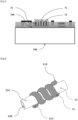
- FIG 7 illustrates a cross-sectional view of an example of integration of the device in a technology of the "Complementary Metal Oxide Semiconductor” (CMOS) type.
- CMOS Complementary Metal Oxide Semiconductor
- the device according to the invention is integrated in Above IC (Integrated Circuit), that is to say above a passivation layer 79A and a silicon substrate 79B.
- Above IC Integrated Circuit
- the device according to the invention can be integrated above the passivation layer 79A so that the device can be in contact with the air, therefore for example in contact with a gas or a volatile organic compound present in the air.
- the first pattern 71 is a spiral inductance made above a passivation layer 79A.
- the second pattern 72 is arranged between the turns of the spiral inductance of the first pattern 71 and is in electrical contact with them.
- the spiral inductance of the first pattern 71 may be square, hexagonal, octagonal or circular in shape.
- the second pattern 72 may be of a shape similar to that of the first pattern.
- the device can be produced with a first and a second pattern in the form of circular spirals.
- These patterns can be produced using printing technologies on flexible or even stretchable supports, typically by screen printing or inkjet, for example with silver ink.
- the device comprises an insulating substrate, on which the patterns rest, having low relative permittivities ⁇ r , in particular less than 5 and thicknesses ranging from a few micrometers to several hundred micrometers.
- the insulating substrate is for example of the paper, plastic or elastomer type.
- the second pattern comprises a second material sensitive to pressure or mechanical stress and whose resistivity changes depending on the force (pressure or stress) applied.
- piezoresistive materials and in particular semiconductors can be used. Such a device could be used as a force or pressure sensor.
- Such a device can be advantageously used to produce a sensor for gases, vapors or VOCs, for which the reactions take place on the surface rather than in volume, and for which large silicon surfaces are not suitable because they are expensive, rigid and heavy.
- Such a device comprising patterns on a flexible support is flexible, conformable and light in addition to being inexpensive.
- FIG 8 illustrates a three-dimensional view of a first variant of a second embodiment comprising a first pattern 81 having a first end 81A and a second end 81B and corresponding to a winding or coil around a second pattern 82 in the form of a right and hollow circular cylinder, the second pattern defining an exterior surface 82A and an interior surface 82B.
- the second pattern defines an interior space which allows the passage of a liquid, gas or solid or a mixture thereof from one end of the second pattern to an opposite end of the second pattern.
- This first variant of a second embodiment also comprises a means for determining (not shown) the inductance of the assembly formed by the first pattern and the second pattern.
- a liquid may pass through the interior space of the second pattern, from a first end to an opposite end.
- the impedance of the second pattern will evolve continuously as a function of the concentration of this specific gas when it comes into contact with the second pattern.
- the inductance of the assembly formed by the first pattern and the second pattern therefore evolves continuously as a function of the measurand.
- the device makes it possible, for example, to monitor pollution of a liquid by a gas inside the hollow cylinder.
- the first pattern is arranged in such a manner that a liquid, solid or gas passing from a first end of the second pattern to an opposite end of the second pattern contacts the second pattern but does not contact the first pattern.
- the device can be adapted such that the first pattern can be in contact with the solid, liquid or gas passing from one end of the second pattern to an opposite end of the second pattern.
- FIG 9 illustrates a three-dimensional view of a second variant of the second embodiment comprising a first pattern 91 having a first end 91A and a second end 91B and a second pattern 92 having a first end 92A and a second end 92B.
- the assembly formed by the first pattern and the second pattern corresponds to a cylinder for connecting a first cylinder 93 to a second cylinder 94.
- This second variant of a second embodiment also comprises a means of determination (not shown) of the inductance of the assembly formed by the first pattern and the second pattern.
- the first pattern and the second pattern are arranged such that a liquid, solid or gas passing from a first end of the first pattern to an opposite end of the first pattern comes into contact with the first pattern and the second pattern.
Landscapes
- Physics & Mathematics (AREA)
- General Physics & Mathematics (AREA)
- Spectroscopy & Molecular Physics (AREA)
- Engineering & Computer Science (AREA)
- Power Engineering (AREA)
- Investigating Or Analyzing Materials By The Use Of Electric Means (AREA)
- Measuring Instrument Details And Bridges, And Automatic Balancing Devices (AREA)
Claims (14)
- Vorrichtung zum Bestimmen einer Messgröße, Folgendes umfassend:- ein erstes Muster (11, 61, 71, 81, 91), das aus einem ersten leitfähigen Material besteht, wobei das erste Muster eine erste Impedanz aufweist und ein erstes Ende (11A, 61A, 81A, 91A) und ein zweites Ende (11B, 61B, 81B, 91B), das von dem ersten Ende entfernt ist, aufweist,- ein zweites Muster (12, 62, 72, 82, 92), das mindestens zwischen dem ersten Ende und dem zweiten Ende angeordnet ist und das erste Muster umschreibt, wobei das zweite Muster derart in elektrischem Kontakt mit dem ersten Muster steht, dass eine elektrische Verbindung zwischen mindestens zwei Punkten des ersten Musters hergestellt wird, wobei das zweite Muster aus einem zweiten Material besteht und eine zweite Impedanz aufweist, die sich kontinuierlich in Abhängigkeit von der Messgröße ändert, sodass sich die Induktivität der von der ersten Muster und dem zweiten Muster gebildeten Anordnung kontinuierlich in Abhängigkeit von der Messgröße ändert,- ein Mittel zum Bestimmen (13) der Induktivität der von dem ersten Muster und dem zweiten Muster gebildeten Anordnung.
- Vorrichtung nach dem vorhergehenden Anspruch, wobei das erste leitfähige Material gegenüber der Änderung der Messgröße nicht empfindlich oder wenig empfindlich ist.
- Vorrichtung nach einem der vorhergehenden Ansprüche, wobei das zweite Material ein Material ist, das eine Leitfähigkeit aufweist, die sich kontinuierlich in Abhängigkeit von der Messgröße ändert.
- Vorrichtung nach Anspruch 3, wobei das zweite Material ein Material ist, dessen Leitfähigkeit zunimmt, wenn der Wert der Messgröße zunimmt.
- Vorrichtung nach Anspruch 3, wobei das zweite Material ein Material ist, dessen Leitfähigkeit abnimmt, wenn der Wert der Messgröße zunimmt.
- Vorrichtung nach einem der vorhergehenden Ansprüche, wobei die von dem ersten Muster und dem zweiten Muster gebildete Anordnung im Wesentlichen zweidimensional ist.
- Vorrichtung nach einem der Ansprüche 1 bis 5, wobei die von dem ersten Muster und dem zweiten Muster gebildete Anordnung im Wesentlichen dreidimensional ist.
- Vorrichtung nach Anspruch 7, wobei das zweite Muster die Form eines Hohlzylinders aufweist, der eine Außenfläche (82A) und eine Innenfläche (82B) definiert,
wobei das erste Muster um das zweite Muster oder zusätzlich innerhalb des zweiten Musters derart gewickelt ist, dass das erste Muster in Kontakt mit der Außenfläche des zweiten Musters oder zusätzlich mit der Innenfläche des zweiten Musters steht und/oder in der Dicke des zweiten Musters liegt. - Vorrichtung nach einem der vorhergehenden Ansprüche, wobei das erste Muster die Form einer Spirale mit n Windungen hat oder Mäander aufweist.
- Vorrichtung nach Anspruch 9, wobei das zweite Muster die Form einer Spirale mit m Windungen, wobei m ≤ n, hat oder Mäander aufweist.
- Vorrichtung nach einem der vorhergehenden Ansprüche, umfassend ein Substrat (19, 79), das einen Träger des ersten Musters und des zweiten Musters bildet.
- Vorrichtung nach einem der vorhergehenden Ansprüche, wobei die Messgröße aus einer Liste ausgewählt ist, die Folgendes umfasst: ein Gas oder eine Gaskonzentration, eine Feuchtigkeit oder einen Feuchtigkeitsgehalt, einen Dampf, eine flüchtige organische Verbindung, VOC, oder eine Konzentration einer VOC, eine Kraft oder einen Druck, eine Temperatur, eine sichtbare, Infrarot- oder Ultraviolett-Strahlung, ein Molekül von Interesse oder eine Konzentration eines Moleküls von Interesse.
- Vorrichtung nach einem der vorhergehenden Ansprüche, wobei das Mittel zum Bestimmen der Induktivität ein Induktivitätsmessgerät oder einen Vektor-Netzwerkanalysator umfassen kann.
- Vorrichtung nach Anspruch 13, wobei das Mittel zum Bestimmen (13) der Induktivität ein Induktivitätsmessgerät umfasst.
Applications Claiming Priority (2)
| Application Number | Priority Date | Filing Date | Title |
|---|---|---|---|
| FR1911713A FR3102242B1 (fr) | 2019-10-18 | 2019-10-18 | Capteur a variation d’impedance ou d’inductance consecutive a une variation d’un mesurande |
| PCT/EP2020/078850 WO2021074193A1 (fr) | 2019-10-18 | 2020-10-14 | Capteur a variation d'impedance ou d'inductance consecutive a une variation d'un mesurande |
Publications (2)
| Publication Number | Publication Date |
|---|---|
| EP4045878A1 EP4045878A1 (de) | 2022-08-24 |
| EP4045878B1 true EP4045878B1 (de) | 2024-11-06 |
Family
ID=69468775
Family Applications (1)
| Application Number | Title | Priority Date | Filing Date |
|---|---|---|---|
| EP20789615.0A Active EP4045878B1 (de) | 2019-10-18 | 2020-10-14 | Sensor mit induktivitätsänderung infolge einer änderung einer messgrösse |
Country Status (4)
| Country | Link |
|---|---|
| US (1) | US11892489B2 (de) |
| EP (1) | EP4045878B1 (de) |
| FR (1) | FR3102242B1 (de) |
| WO (1) | WO2021074193A1 (de) |
Families Citing this family (1)
| Publication number | Priority date | Publication date | Assignee | Title |
|---|---|---|---|---|
| US20230375492A1 (en) * | 2022-02-09 | 2023-11-23 | Purdue Research Foundation | Methods and apparatus for sensing volatile organic compounds and gases released from electrochemical cells |
Citations (6)
| Publication number | Priority date | Publication date | Assignee | Title |
|---|---|---|---|---|
| DE3638286A1 (de) * | 1986-11-10 | 1988-05-11 | Siemens Ag | Elektrisches bauelement aus keramik mit mehrlagenmetallisierung und verfahren zu seiner herstellung |
| US20050284231A1 (en) * | 2002-08-06 | 2005-12-29 | Werner Zimmerman | Stress/extension-measuring sensor and method for measuring stress/expansion |
| EP2084521A2 (de) * | 2006-11-21 | 2009-08-05 | Amersham Biosciences Corp. | Zusammenbau und nutzung von rfid-sensoren in behältern |
| US20140019067A1 (en) * | 2010-12-23 | 2014-01-16 | General Electric Company | Temperature-independent chemical and biological sensors |
| US20140028327A1 (en) * | 2012-07-26 | 2014-01-30 | General Electric Company | Method for sensor reader calibration |
| WO2019119981A1 (zh) * | 2017-12-20 | 2019-06-27 | 广东爱晟电子科技有限公司 | 一种复合热敏电阻芯片及其制备方法 |
Family Cites Families (8)
| Publication number | Priority date | Publication date | Assignee | Title |
|---|---|---|---|---|
| CN1251255C (zh) | 2004-05-10 | 2006-04-12 | 阎跃军 | 可调电感器 |
| US7498802B2 (en) | 2006-07-10 | 2009-03-03 | 3M Innovative Properties Company | Flexible inductive sensor |
| US8159347B2 (en) * | 2008-09-25 | 2012-04-17 | General Electric Company | Sensors having gap based sensing devices and methods of making and using the same |
| CN106160268B (zh) * | 2015-05-15 | 2020-11-06 | 松下知识产权经营株式会社 | 异物检测装置、无线送电装置以及无线电力传送系统 |
| US10725117B2 (en) * | 2018-05-30 | 2020-07-28 | Landis+Gyr Technologies, Llc | Component leak detection apparatuses and methods |
| US20200012008A1 (en) * | 2018-07-08 | 2020-01-09 | Wayne State University | Parity-time (pt)-symmetric wireless telemetric sensors and systems |
| US10846494B2 (en) * | 2019-01-03 | 2020-11-24 | The Boeing Company | Radio-frequency identification device for indicating a temperature history of a composite structure |
| US10812145B1 (en) * | 2019-06-21 | 2020-10-20 | eTEP Inc. | Packaging system with detection of environmental conditions |
-
2019
- 2019-10-18 FR FR1911713A patent/FR3102242B1/fr active Active
-
2020
- 2020-10-14 WO PCT/EP2020/078850 patent/WO2021074193A1/fr not_active Ceased
- 2020-10-14 US US17/765,426 patent/US11892489B2/en active Active
- 2020-10-14 EP EP20789615.0A patent/EP4045878B1/de active Active
Patent Citations (6)
| Publication number | Priority date | Publication date | Assignee | Title |
|---|---|---|---|---|
| DE3638286A1 (de) * | 1986-11-10 | 1988-05-11 | Siemens Ag | Elektrisches bauelement aus keramik mit mehrlagenmetallisierung und verfahren zu seiner herstellung |
| US20050284231A1 (en) * | 2002-08-06 | 2005-12-29 | Werner Zimmerman | Stress/extension-measuring sensor and method for measuring stress/expansion |
| EP2084521A2 (de) * | 2006-11-21 | 2009-08-05 | Amersham Biosciences Corp. | Zusammenbau und nutzung von rfid-sensoren in behältern |
| US20140019067A1 (en) * | 2010-12-23 | 2014-01-16 | General Electric Company | Temperature-independent chemical and biological sensors |
| US20140028327A1 (en) * | 2012-07-26 | 2014-01-30 | General Electric Company | Method for sensor reader calibration |
| WO2019119981A1 (zh) * | 2017-12-20 | 2019-06-27 | 广东爱晟电子科技有限公司 | 一种复合热敏电阻芯片及其制备方法 |
Also Published As
| Publication number | Publication date |
|---|---|
| FR3102242B1 (fr) | 2021-11-05 |
| WO2021074193A1 (fr) | 2021-04-22 |
| FR3102242A1 (fr) | 2021-04-23 |
| US20220357381A1 (en) | 2022-11-10 |
| EP4045878A1 (de) | 2022-08-24 |
| US11892489B2 (en) | 2024-02-06 |
Similar Documents
| Publication | Publication Date | Title |
|---|---|---|
| US8990025B2 (en) | Temperature-independent chemical and biological sensors | |
| EP2602598B1 (de) | Bolometrischer Detektor für elektromagnetische Strahlung im Spektralbereich von Terahertz und Matrix, die solche Detektoren umfasst | |
| US9037418B2 (en) | Highly selective chemical and biological sensors | |
| US10634637B2 (en) | Highly selective chemical and biological sensors | |
| Briand et al. | Making environmental sensors on plastic foil | |
| Mc Gee et al. | A review of chipless remote sensing solutions based on RFID technology | |
| EP2338030B1 (de) | Magnetpositionssensor mit feldrichtungsmessung und flusskollektor | |
| JP5596692B2 (ja) | ギャップ式感知装置を有するセンサ | |
| CN101842689B (zh) | 基于暴露材料的渐进腐蚀的湿度传感器 | |
| US8456620B2 (en) | Enabling spectrometry on IR sensors using metamaterials | |
| US20100176822A1 (en) | Nanowire sensor | |
| EP2013612A1 (de) | Mikroheizplatten-halbleiter-gassensor | |
| EP4184125B1 (de) | Vorrichtung zur messung mindestens einer physikalischen grösse und verfahren zur bestimmung davon | |
| EP4045878A1 (de) | Sensor mit impedanz- oder induktivitätsänderung nach einer änderung einer messgrösse | |
| Bhattacharyya et al. | Resistive and capacitive measurement of nano-structured gas sensors | |
| EP1963779B1 (de) | Vorrichtung zur aufnahme einer lagerung mit einem system zur erkennung der auf die lagerung gelegten last. | |
| US10846584B2 (en) | Printed electronic film for dust sensing on PV cells and reporting via RFID tags | |
| US7514693B2 (en) | Multidirectional ultraviolet sensor | |
| US20250292053A1 (en) | Systems and methods for relative damping of antennas for sensing and tuning in the frequency domain | |
| JP5442648B2 (ja) | 赤外線センサ | |
| Mutinati et al. | CMOS-integrable ultrathin SnO2 layer for smart gas sensor devices | |
| EP2435798B1 (de) | Messgerät mit einem elektromagnetischen diffusor | |
| Li et al. | Design and Implementation of CMOS-MEMS Schottky Gas Sensor With Asymmetric Metal Contacts for Performance Enhancement at Room Temperature | |
| Buzanovskii | Gas chemical nanosensors with sensing elements based on tungsten oxides | |
| EP4248067A1 (de) | Verbundteil, insbesondere für ein flugzeugturbinentriebwerk |
Legal Events
| Date | Code | Title | Description |
|---|---|---|---|
| STAA | Information on the status of an ep patent application or granted ep patent |
Free format text: STATUS: UNKNOWN |
|
| STAA | Information on the status of an ep patent application or granted ep patent |
Free format text: STATUS: THE INTERNATIONAL PUBLICATION HAS BEEN MADE |
|
| PUAI | Public reference made under article 153(3) epc to a published international application that has entered the european phase |
Free format text: ORIGINAL CODE: 0009012 |
|
| STAA | Information on the status of an ep patent application or granted ep patent |
Free format text: STATUS: REQUEST FOR EXAMINATION WAS MADE |
|
| 17P | Request for examination filed |
Effective date: 20220503 |
|
| AK | Designated contracting states |
Kind code of ref document: A1 Designated state(s): AL AT BE BG CH CY CZ DE DK EE ES FI FR GB GR HR HU IE IS IT LI LT LU LV MC MK MT NL NO PL PT RO RS SE SI SK SM TR |
|
| DAV | Request for validation of the european patent (deleted) | ||
| DAX | Request for extension of the european patent (deleted) | ||
| GRAP | Despatch of communication of intention to grant a patent |
Free format text: ORIGINAL CODE: EPIDOSNIGR1 |
|
| STAA | Information on the status of an ep patent application or granted ep patent |
Free format text: STATUS: GRANT OF PATENT IS INTENDED |
|
| RIC1 | Information provided on ipc code assigned before grant |
Ipc: G01N 27/22 20060101ALN20240508BHEP Ipc: G01D 5/12 20060101ALN20240508BHEP Ipc: G01L 9/00 20060101ALI20240508BHEP Ipc: G01K 7/36 20060101ALI20240508BHEP Ipc: G01L 1/14 20060101ALI20240508BHEP Ipc: G01K 7/16 20060101ALI20240508BHEP Ipc: G01J 5/34 20060101ALI20240508BHEP Ipc: G01J 5/20 20060101ALI20240508BHEP Ipc: G01D 21/00 20060101AFI20240508BHEP |
|
| INTG | Intention to grant announced |
Effective date: 20240528 |
|
| GRAJ | Information related to disapproval of communication of intention to grant by the applicant or resumption of examination proceedings by the epo deleted |
Free format text: ORIGINAL CODE: EPIDOSDIGR1 |
|
| STAA | Information on the status of an ep patent application or granted ep patent |
Free format text: STATUS: REQUEST FOR EXAMINATION WAS MADE |
|
| GRAP | Despatch of communication of intention to grant a patent |
Free format text: ORIGINAL CODE: EPIDOSNIGR1 |
|
| STAA | Information on the status of an ep patent application or granted ep patent |
Free format text: STATUS: GRANT OF PATENT IS INTENDED |
|
| INTC | Intention to grant announced (deleted) | ||
| INTG | Intention to grant announced |
Effective date: 20240812 |
|
| RIC1 | Information provided on ipc code assigned before grant |
Ipc: G01N 27/22 20060101ALN20240802BHEP Ipc: G01D 5/12 20060101ALN20240802BHEP Ipc: G01L 9/00 20060101ALI20240802BHEP Ipc: G01K 7/36 20060101ALI20240802BHEP Ipc: G01L 1/14 20060101ALI20240802BHEP Ipc: G01K 7/16 20060101ALI20240802BHEP Ipc: G01J 5/34 20220101ALI20240802BHEP Ipc: G01J 5/20 20060101ALI20240802BHEP Ipc: G01D 21/00 20060101AFI20240802BHEP |
|
| GRAS | Grant fee paid |
Free format text: ORIGINAL CODE: EPIDOSNIGR3 |
|
| GRAA | (expected) grant |
Free format text: ORIGINAL CODE: 0009210 |
|
| STAA | Information on the status of an ep patent application or granted ep patent |
Free format text: STATUS: THE PATENT HAS BEEN GRANTED |
|
| AK | Designated contracting states |
Kind code of ref document: B1 Designated state(s): AL AT BE BG CH CY CZ DE DK EE ES FI FR GB GR HR HU IE IS IT LI LT LU LV MC MK MT NL NO PL PT RO RS SE SI SK SM TR |
|
| REG | Reference to a national code |
Ref country code: GB Ref legal event code: FG4D Free format text: NOT ENGLISH |
|
| REG | Reference to a national code |
Ref country code: CH Ref legal event code: EP |
|
| REG | Reference to a national code |
Ref country code: DE Ref legal event code: R096 Ref document number: 602020040926 Country of ref document: DE |
|
| REG | Reference to a national code |
Ref country code: IE Ref legal event code: FG4D Free format text: LANGUAGE OF EP DOCUMENT: FRENCH |
|
| REG | Reference to a national code |
Ref country code: LT Ref legal event code: MG9D |
|
| REG | Reference to a national code |
Ref country code: NL Ref legal event code: MP Effective date: 20241106 |
|
| PG25 | Lapsed in a contracting state [announced via postgrant information from national office to epo] |
Ref country code: PT Free format text: LAPSE BECAUSE OF FAILURE TO SUBMIT A TRANSLATION OF THE DESCRIPTION OR TO PAY THE FEE WITHIN THE PRESCRIBED TIME-LIMIT Effective date: 20250306 Ref country code: HR Free format text: LAPSE BECAUSE OF FAILURE TO SUBMIT A TRANSLATION OF THE DESCRIPTION OR TO PAY THE FEE WITHIN THE PRESCRIBED TIME-LIMIT Effective date: 20241106 Ref country code: IS Free format text: LAPSE BECAUSE OF FAILURE TO SUBMIT A TRANSLATION OF THE DESCRIPTION OR TO PAY THE FEE WITHIN THE PRESCRIBED TIME-LIMIT Effective date: 20250306 |
|
| PG25 | Lapsed in a contracting state [announced via postgrant information from national office to epo] |
Ref country code: NL Free format text: LAPSE BECAUSE OF FAILURE TO SUBMIT A TRANSLATION OF THE DESCRIPTION OR TO PAY THE FEE WITHIN THE PRESCRIBED TIME-LIMIT Effective date: 20241106 Ref country code: FI Free format text: LAPSE BECAUSE OF FAILURE TO SUBMIT A TRANSLATION OF THE DESCRIPTION OR TO PAY THE FEE WITHIN THE PRESCRIBED TIME-LIMIT Effective date: 20241106 |
|
| REG | Reference to a national code |
Ref country code: AT Ref legal event code: MK05 Ref document number: 1739796 Country of ref document: AT Kind code of ref document: T Effective date: 20241106 |
|
| PG25 | Lapsed in a contracting state [announced via postgrant information from national office to epo] |
Ref country code: BG Free format text: LAPSE BECAUSE OF FAILURE TO SUBMIT A TRANSLATION OF THE DESCRIPTION OR TO PAY THE FEE WITHIN THE PRESCRIBED TIME-LIMIT Effective date: 20241106 |
|
| PG25 | Lapsed in a contracting state [announced via postgrant information from national office to epo] |
Ref country code: ES Free format text: LAPSE BECAUSE OF FAILURE TO SUBMIT A TRANSLATION OF THE DESCRIPTION OR TO PAY THE FEE WITHIN THE PRESCRIBED TIME-LIMIT Effective date: 20241106 |
|
| PG25 | Lapsed in a contracting state [announced via postgrant information from national office to epo] |
Ref country code: NO Free format text: LAPSE BECAUSE OF FAILURE TO SUBMIT A TRANSLATION OF THE DESCRIPTION OR TO PAY THE FEE WITHIN THE PRESCRIBED TIME-LIMIT Effective date: 20250206 |
|
| PG25 | Lapsed in a contracting state [announced via postgrant information from national office to epo] |
Ref country code: GR Free format text: LAPSE BECAUSE OF FAILURE TO SUBMIT A TRANSLATION OF THE DESCRIPTION OR TO PAY THE FEE WITHIN THE PRESCRIBED TIME-LIMIT Effective date: 20250207 Ref country code: LV Free format text: LAPSE BECAUSE OF FAILURE TO SUBMIT A TRANSLATION OF THE DESCRIPTION OR TO PAY THE FEE WITHIN THE PRESCRIBED TIME-LIMIT Effective date: 20241106 Ref country code: AT Free format text: LAPSE BECAUSE OF FAILURE TO SUBMIT A TRANSLATION OF THE DESCRIPTION OR TO PAY THE FEE WITHIN THE PRESCRIBED TIME-LIMIT Effective date: 20241106 |
|
| PG25 | Lapsed in a contracting state [announced via postgrant information from national office to epo] |
Ref country code: PL Free format text: LAPSE BECAUSE OF FAILURE TO SUBMIT A TRANSLATION OF THE DESCRIPTION OR TO PAY THE FEE WITHIN THE PRESCRIBED TIME-LIMIT Effective date: 20241106 |
|
| PG25 | Lapsed in a contracting state [announced via postgrant information from national office to epo] |
Ref country code: RS Free format text: LAPSE BECAUSE OF FAILURE TO SUBMIT A TRANSLATION OF THE DESCRIPTION OR TO PAY THE FEE WITHIN THE PRESCRIBED TIME-LIMIT Effective date: 20250206 |
|
| PG25 | Lapsed in a contracting state [announced via postgrant information from national office to epo] |
Ref country code: SM Free format text: LAPSE BECAUSE OF FAILURE TO SUBMIT A TRANSLATION OF THE DESCRIPTION OR TO PAY THE FEE WITHIN THE PRESCRIBED TIME-LIMIT Effective date: 20241106 |
|
| PG25 | Lapsed in a contracting state [announced via postgrant information from national office to epo] |
Ref country code: DK Free format text: LAPSE BECAUSE OF FAILURE TO SUBMIT A TRANSLATION OF THE DESCRIPTION OR TO PAY THE FEE WITHIN THE PRESCRIBED TIME-LIMIT Effective date: 20241106 |
|
| PG25 | Lapsed in a contracting state [announced via postgrant information from national office to epo] |
Ref country code: EE Free format text: LAPSE BECAUSE OF FAILURE TO SUBMIT A TRANSLATION OF THE DESCRIPTION OR TO PAY THE FEE WITHIN THE PRESCRIBED TIME-LIMIT Effective date: 20241106 |
|
| PG25 | Lapsed in a contracting state [announced via postgrant information from national office to epo] |
Ref country code: RO Free format text: LAPSE BECAUSE OF FAILURE TO SUBMIT A TRANSLATION OF THE DESCRIPTION OR TO PAY THE FEE WITHIN THE PRESCRIBED TIME-LIMIT Effective date: 20241106 |
|
| PG25 | Lapsed in a contracting state [announced via postgrant information from national office to epo] |
Ref country code: SK Free format text: LAPSE BECAUSE OF FAILURE TO SUBMIT A TRANSLATION OF THE DESCRIPTION OR TO PAY THE FEE WITHIN THE PRESCRIBED TIME-LIMIT Effective date: 20241106 |
|
| PG25 | Lapsed in a contracting state [announced via postgrant information from national office to epo] |
Ref country code: CZ Free format text: LAPSE BECAUSE OF FAILURE TO SUBMIT A TRANSLATION OF THE DESCRIPTION OR TO PAY THE FEE WITHIN THE PRESCRIBED TIME-LIMIT Effective date: 20241106 |
|
| PG25 | Lapsed in a contracting state [announced via postgrant information from national office to epo] |
Ref country code: IT Free format text: LAPSE BECAUSE OF FAILURE TO SUBMIT A TRANSLATION OF THE DESCRIPTION OR TO PAY THE FEE WITHIN THE PRESCRIBED TIME-LIMIT Effective date: 20241106 |
|
| REG | Reference to a national code |
Ref country code: DE Ref legal event code: R097 Ref document number: 602020040926 Country of ref document: DE |
|
| PG25 | Lapsed in a contracting state [announced via postgrant information from national office to epo] |
Ref country code: SE Free format text: LAPSE BECAUSE OF FAILURE TO SUBMIT A TRANSLATION OF THE DESCRIPTION OR TO PAY THE FEE WITHIN THE PRESCRIBED TIME-LIMIT Effective date: 20241106 |
|
| PLBE | No opposition filed within time limit |
Free format text: ORIGINAL CODE: 0009261 |
|
| STAA | Information on the status of an ep patent application or granted ep patent |
Free format text: STATUS: NO OPPOSITION FILED WITHIN TIME LIMIT |
|
| 26N | No opposition filed |
Effective date: 20250807 |
|
| PGFP | Annual fee paid to national office [announced via postgrant information from national office to epo] |
Ref country code: DE Payment date: 20251126 Year of fee payment: 6 |
|
| PGFP | Annual fee paid to national office [announced via postgrant information from national office to epo] |
Ref country code: GB Payment date: 20251029 Year of fee payment: 6 |
|
| PGFP | Annual fee paid to national office [announced via postgrant information from national office to epo] |
Ref country code: FR Payment date: 20251030 Year of fee payment: 6 |