EP4044432A1 - Semiconductor device having conductive via offset structure, power supply structure, and electronic device - Google Patents
Semiconductor device having conductive via offset structure, power supply structure, and electronic device Download PDFInfo
- Publication number
- EP4044432A1 EP4044432A1 EP20864907.9A EP20864907A EP4044432A1 EP 4044432 A1 EP4044432 A1 EP 4044432A1 EP 20864907 A EP20864907 A EP 20864907A EP 4044432 A1 EP4044432 A1 EP 4044432A1
- Authority
- EP
- European Patent Office
- Prior art keywords
- substrate
- protrusion
- semiconductor device
- conductive via
- electrically connected
- Prior art date
- Legal status (The legal status is an assumption and is not a legal conclusion. Google has not performed a legal analysis and makes no representation as to the accuracy of the status listed.)
- Granted
Links
Images






Classifications
-
- H—ELECTRICITY
- H03—ELECTRONIC CIRCUITRY
- H03H—IMPEDANCE NETWORKS, e.g. RESONANT CIRCUITS; RESONATORS
- H03H9/00—Networks comprising electromechanical or electro-acoustic elements; Electromechanical resonators
- H03H9/02—Details
- H03H9/05—Holders or supports
- H03H9/10—Mounting in enclosures
- H03H9/1007—Mounting in enclosures for bulk acoustic wave [BAW] devices
- H03H9/1014—Mounting in enclosures for bulk acoustic wave [BAW] devices the enclosure being defined by a frame built on a substrate and a cap, the frame having no mechanical contact with the BAW device
-
- H—ELECTRICITY
- H10—SEMICONDUCTOR DEVICES; ELECTRIC SOLID-STATE DEVICES NOT OTHERWISE PROVIDED FOR
- H10W—GENERIC PACKAGES, INTERCONNECTIONS, CONNECTORS OR OTHER CONSTRUCTIONAL DETAILS OF DEVICES COVERED BY CLASS H10
- H10W74/00—Encapsulations, e.g. protective coatings
- H10W74/10—Encapsulations, e.g. protective coatings characterised by their shape or disposition
- H10W74/111—Encapsulations, e.g. protective coatings characterised by their shape or disposition the semiconductor body being completely enclosed
-
- H—ELECTRICITY
- H03—ELECTRONIC CIRCUITRY
- H03H—IMPEDANCE NETWORKS, e.g. RESONANT CIRCUITS; RESONATORS
- H03H9/00—Networks comprising electromechanical or electro-acoustic elements; Electromechanical resonators
- H03H9/02—Details
- H03H9/05—Holders or supports
- H03H9/0504—Holders or supports for bulk acoustic wave devices
- H03H9/0514—Holders or supports for bulk acoustic wave devices consisting of mounting pads or bumps
-
- H—ELECTRICITY
- H03—ELECTRONIC CIRCUITRY
- H03H—IMPEDANCE NETWORKS, e.g. RESONANT CIRCUITS; RESONATORS
- H03H9/00—Networks comprising electromechanical or electro-acoustic elements; Electromechanical resonators
- H03H9/46—Filters
- H03H9/54—Filters comprising resonators of piezoelectric or electrostrictive material
- H03H9/56—Monolithic crystal filters
- H03H9/564—Monolithic crystal filters implemented with thin-film techniques
-
- H—ELECTRICITY
- H03—ELECTRONIC CIRCUITRY
- H03H—IMPEDANCE NETWORKS, e.g. RESONANT CIRCUITS; RESONATORS
- H03H9/00—Networks comprising electromechanical or electro-acoustic elements; Electromechanical resonators
- H03H9/46—Filters
- H03H9/54—Filters comprising resonators of piezoelectric or electrostrictive material
- H03H9/56—Monolithic crystal filters
- H03H9/566—Electric coupling means therefor
- H03H9/568—Electric coupling means therefor consisting of a ladder configuration
-
- H—ELECTRICITY
- H10—SEMICONDUCTOR DEVICES; ELECTRIC SOLID-STATE DEVICES NOT OTHERWISE PROVIDED FOR
- H10N—ELECTRIC SOLID-STATE DEVICES NOT OTHERWISE PROVIDED FOR
- H10N30/00—Piezoelectric or electrostrictive devices
-
- H—ELECTRICITY
- H10—SEMICONDUCTOR DEVICES; ELECTRIC SOLID-STATE DEVICES NOT OTHERWISE PROVIDED FOR
- H10N—ELECTRIC SOLID-STATE DEVICES NOT OTHERWISE PROVIDED FOR
- H10N30/00—Piezoelectric or electrostrictive devices
- H10N30/80—Constructional details
- H10N30/88—Mounts; Supports; Enclosures; Casings
-
- H—ELECTRICITY
- H10—SEMICONDUCTOR DEVICES; ELECTRIC SOLID-STATE DEVICES NOT OTHERWISE PROVIDED FOR
- H10W—GENERIC PACKAGES, INTERCONNECTIONS, CONNECTORS OR OTHER CONSTRUCTIONAL DETAILS OF DEVICES COVERED BY CLASS H10
- H10W70/00—Package substrates; Interposers; Redistribution layers [RDL]
- H10W70/60—Insulating or insulated package substrates; Interposers; Redistribution layers
- H10W70/62—Insulating or insulated package substrates; Interposers; Redistribution layers characterised by their interconnections
- H10W70/63—Vias, e.g. via plugs
- H10W70/635—Through-vias
-
- H—ELECTRICITY
- H10—SEMICONDUCTOR DEVICES; ELECTRIC SOLID-STATE DEVICES NOT OTHERWISE PROVIDED FOR
- H10W—GENERIC PACKAGES, INTERCONNECTIONS, CONNECTORS OR OTHER CONSTRUCTIONAL DETAILS OF DEVICES COVERED BY CLASS H10
- H10W72/00—Interconnections or connectors in packages
- H10W72/01—Manufacture or treatment
- H10W72/012—Manufacture or treatment of bump connectors, dummy bumps or thermal bumps
Definitions
- Embodiments of the present disclosure relate to the field of semiconductors, and in particular, to a semiconductor device, a power supply structure of a semiconductor device, and an electronic device having the semiconductor device or the power supply structure.
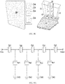
- FIG. 9A is an abstract circuit diagram of a filter with bulk acoustic wave resonators.
- the resonators includes five series resonators Rs1-5 and four parallel resonators Rp1-4.
- the filter further includes an input terminal Input, an output terminal Output, and four ground terminals GND
- FIG. 9B is a top view of a conventional packaging structure of the filter shown in FIG. 9A .
- FIG. 9C is a sectional view of the packaging structure along line M-M' in FIG. 9B , and shows a part of the packaging structure above a line N-N' in FIG. 9B .
- the packaging structure shown in FIGS. 9B and 9C includes:
- FIG. 9D also shows a perspective view of the second substrate 20 (including the first protrusion 21 and the second protrusions 22 located thereon).
- the packaging structure is hardly decreased in dimension in a lateral direction.
- the present disclosure is provided to offset a via in a second substrate towards an inner side to reduce a dimension of a second protrusion, so that a packaging structure can be reduced in dimension in a lateral direction.
- a semiconductor device includes: a first substrate and a second substrate opposite to each other, an accommodation space being formed between the first substrate and the second substrate; a semiconductor element provided in the accommodation space and arranged on the first substrate, the semiconductor element having a pin for electrical connection; an annular support protrusion provided between the first substrate and the second substrate, the annular support protrusion, a first side of the first substrate and a first side of the second substrate defining the accommodation space; at least one second protrusion provided within the accommodation space and arranged at an inner side of the annular support protrusion; a conductor layer provided on a surface of the at least one second protrusion, the conductor layer including a first connection portion and a via connection portion electrically connected to each other, the first connection portion being arranged at an end surface of the at least one second protrusion and electrically connected with the pin, and the via connection portion extending along the first side of the second substrate; and a conductive via provided at the second substrate
- the conductive via is located at an inner side of a corresponding one of the at least one second protrusion or is spaced apart from a corresponding one of the at least one second protrusion, or the conductive via does not coincide with an end surface of a corresponding one of the at least one second protrusion.
- the semiconductor device further includes a bonding layer arranged on a surface of the annular support protrusion.
- the bonding layer is electrically isolated from the conductor layer.
- the at least one second protrusion includes a plurality of second protrusions spaced apart from each other, and at least one of the plurality of second protrusions is integrally formed with the annular support protrusion.
- At least one pin corresponding to the at least one second protrusion has an L-shaped contact surface
- the L-shaped contact surface has a shortest side with a length not greater than 50 ⁇ m
- all sides of the L-shaped contact surface have lengths not less than 5 ⁇ m.
- At least one pin corresponding to the at least one second protrusion has a rectangular contact surface, the rectangular contact surface has a shortest side with a length not greater than 50 ⁇ m, and all sides of the rectangular contact surface have lengths not less than 5 ⁇ m.
- at least one of the at least one second protrusion includes a plurality of sub-protrusions spaced apart from each other.
- the semiconductor device further includes a pad and a solder ball arranged on a second side of the second substrate and electrically connected to each other.
- the pad is electrically connected to the conductive via.
- the conductive via passes throughout the second substrate in a thickness of the second substrate.
- a protective layer is provided at a side or sides where either or both ends of the conductive via are located.
- the second substrate is provided with a recessed portion on the second side, and the recessed portion corresponds to the conductive via.
- the recessed portion has a horizontal bottom portion and inclined sidewalls.
- the conductive via has an upper end located at the horizontal bottom portion. The conductive material in the conductive via is in contact with a conductive material layer of the pad formed on the horizontal bottom portion and the inclined sidewalls of the recessed portion.
- a stepped portion is provided on the inclined sidewalls.
- a protective layer is provided at a side where a lower end of the conductive via is located.
- solder ball is located within the recessed portion.
- the recessed portion has a depth greater than half of a thickness of the second substrate.
- the semiconductor device is a filter.
- the semiconductor element includes at least one bulk acoustic wave resonator.
- the at least one bulk acoustic wave resonator includes a bottom electrode, a piezoelectric layer, and a top electrode, and an electrode of a corresponding one of the at least one bulk acoustic wave resonator is electrically connected to the pin.
- a power supply structure for a semiconductor device.
- the power supply structure includes: a protrusion arranged between a first substrate and a second substrate opposite to each other, the protrusion protruding from the second substrate towards the first substrate; and a conductor layer provided on a surface of the protrusion.
- a portion of the conductor layer located on an end surface of the protrusion is electrically connected to a pin, and the pin is configured to supply power to a semiconductor element.
- the conductor layer has an extension portion extending inwardly along the second substrate, the second substrate is provided with a conductive via therein, and the conductive via is electrically connected to the extension portion of the conductor layer.
- the conductive via is located at an inner side of the protrusion or is spaced apart from the protrusion, or the conductive via does not coincide with the end surfaces of the protrusion.
- the protrusion comprises at least one second protrusion
- the power supply structure further includes an annular packaging protrusion as a first protrusion.
- the first protrusion is arranged between the first substrate and the second substrate to form an accommodation space therebetween, and the at least one second protrusion is located at an inner side of the first protrusion.
- the at least one second protrusion includes a plurality of protrusions spaced apart from each other, and at least one of the at least one second protrusion is integrally formed with the first protrusion.
- an electronic device including the semiconductor device or the power supply structure as described above.
- a method for manufacturing a semiconductor device includes: providing a first substrate and a second substrate opposite to each other and providing an annular support protrusion between the first substrate and the second substrate, the annular support protrusion, a first side of the first substrate and a first side of the second substrate defining an accommodation space; providing a semiconductor element in the accommodation space, the semiconductor element being arranged on the first substrate and having a pin for electrical connection; providing at least one second protrusion within the accommodation space, the at least one second protrusion being arranged at an inner side of the annular support protrusion; providing a conductor layer on a surface of the at least one second protrusion, the conductor layer including a first connection portion and a via connection portion electrically connected to each other, the first connection portion being arranged at an end surface of the at least one second protrusion and electrically connected with the pin, and the via connection portion extending along the first side of the second substrate; and providing a conductive via in the second
- the conductive via is located at an inner side of a corresponding one of the at least one second protrusion or is spaced apart from a corresponding one of the at least one second protrusion, or the conductive via does not coincide with an end surface of a corresponding one of the at least one second protrusion.
- the providing a conductive via in the second substrate includes: processing a blind hole on the first side of the second substrate, the blind hole having a depth not less than half of a thickness of the second substrate; filling the conductive material in the blind hole; processing a recessed portion on a second side of the second substrate, the recessed portion having a depth not less than half of the thickness of the second substrate, and the second side of the second substrate being opposite to the first side of the second substrate; and providing a conductive material layer within the recessed portion, the conductive material layer being electrically connected to the conductive material in the blind hole.
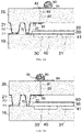
- FIG. 1 is a schematic partial sectional view of a packaging structure with an offset conductive via according to an exemplary embodiment A100 of the present disclosure.
- the packaging structure includes:
- the conductive via 23 is arranged to be spaced from the second protrusion 22, rather than being arranged therein. In this way, the conductive via 23, the pad 81 and the solder ball 90 are translated towards a resonator side. Meanwhile, the conductor layer 72 also extends towards the resonator side along a lower surface of the substrate 20. Since the second protrusion 22 is not provided with a conductive via therein in this case, the second protrusion 22 has a lateral dimension which is significantly reduced, such that the first protrusion 21 is translated inwardly. Therefore, the packaging structure has a smaller lateral dimension than that of the conventional packaging structure.
- the conductive via 23 is located at an inner side of the second protrusion 22 or is spaced apart from the second protrusion 22. Alternatively, the conductive via 23 does not coincide with a corresponding pin, such as a pin C3 in FIG. 5 .
- FIG. 2 is a schematic partial sectional view of a packaging structure with an offset conductive via according to another exemplary embodiment A200 of the present disclosure.
- the first protrusion 21 moves further inwardly, and is combined with the second protrusion 22 to integrally form a protrusion 24.
- the conductor layer 72 is ensured to be spaced apart from the bonding layer 73 by a predetermined gap, i.e., an electrical isolation, thereby forming the structure shown in FIG. 2 .
- the packaging structure shown in FIG. 2 has a lateral dimension which is further reduced. As shown in FIG.
- the bonding layer 73 is arranged at a left side of an end surface of the protrusion 24, the conductor layer 72 is arranged at a right side of an end surface of the protrusion 24, and the bonding layer 73 is electrically isolated from the conductor layer 72.
- the conductive via 23 is provided with a protective layer or protection layer(s) 82/83 arranged at an upper end and/or a lower end thereof.
- the protective layer 82/83 is a protective layer configured to prevent moisture from entering the conductive via 23. Further, in addition to the position shown in FIGS.
- the protective layer 82 may be located above the pad 81, and the protective layer 83 may be located below the conductor layer 72.
- the protective layer may be made of a metal such as chromium, gold, titanium in a case of electrical conduction, or may be made of a non-metal such as silicon dioxide, silicon carbide, aluminum oxide, aluminum nitride, or other dielectric materials without the electrical conduction.
- a protective layer is provided at the lower end of the conductive via.
- a solder ball 91 is provided within a recessed portion formed at the upper end of the conductive via, or the solder ball 90 is moved to a position of the solder ball 91, which can also function as the protective layer.
- the protective layer or the protection layer can enhance sealing performance of the conductive via.
- the protective layer may have the same coating area as that of the conductor layer, or the protective layer may have a different coating area from that of the conductor layer, which is not limited thereto.
- the conductive via 23 is blocked at an end of a bonding interface and thus blocked by the conductor layer, the lower electrode located below the conductor layer, and the first substrate. Accordingly, the conductor metal 80 filled in the conductive via 23 cannot leak out.
- the packaging structures shown in the embodiment A100 of FIG. 1 and the embodiment A200 of FIG. 2 since only one layer of the conductor metal or conductor layer 72 is arranged at an opening of the conductive via 23 at the lower surface of the second substrate 20, the conductor metal 80 filled in the conductive via 23 may not being blocked by the conductor layer 72, which may result in leakage.
- the conductive via 23 since passing throughout the second substrate 20, the conductive via 23 has a relatively long length, which tends to generate a filling defect during filling the conductor metal 80 into the conductive via 23. Accordingly, an impedance of the conductor becomes large or even generates a break, thereby significantly affecting performance and yield of a filter or other electronic devices.
- a funnel-shaped via structure is provided in the packaging structure of the embodiment A100 shown in FIG. 1 or embodiment A200 shown in FIG. 2 .
- the funnel-shaped via structure is formed with a horizontal bottom portion and inclined sidewalls in a region 25 to increase a contact area of the conductor metal 80 and the second substrate 20, thereby increasing the attachment stability of the conductor metal 80.
- the funnel-shaped via structure in the embodiment shown in FIG. 4 .
- the funnel-shaped via structure is additionally provided with a stepped structure on sidewalls thereof, respectively, to further increase the contact area of the metal layer or conductor layer and the second substrate 20.
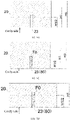
- a method for manufacturing the via structure with the recessed portion shown in FIG. 4 is illustratively described below with reference to FIGS. 5A to 5E .
- FIG. 5A schematically shows a pre-grinding thickness HO, a target grinding thickness HI, and a half-target thickness H1/2 of a packaged wafer.
- FIG 5B shows a step of forming a blind hole on a cavity side of the second substrate.
- the blind hole 23 is formed on the cavity side of the second substrate 20 through deep silicon etching (DSI) or other processes, and the blind hole has a depth not less than H1/2.
- DSI deep silicon etching
- FIG. 5C shows a step of filling the blind hole with the conductor metal.
- the blind hole 23 is filled with the conductor metal 80 by processes such as sputtering and electroplating.
- a filling defect F0 is generally formed at a blind end of the blind hole 23.
- FIG. 5D shows a step of grinding and processing an opposite side opposite to the cavity side of the second substrate to achieve the target thickness HI.
- FIG. 5E shows a step of processing a cavity on the opposite side opposite to the cavity side of the second substrate.
- the opposite side of the second substrate 20 is etched to form a trapezoidal hole with a depth greater than H1/2, and the metal filling defect F0 containing a small section of the conductor metal 80 therebelow is also removed during the etching.
- the blind hole 23 is formed to be a through hole, and there is no meal filling defect in the remaining section of the conductor metal.
- FIG. 5F shows a step of depositing a metal layer within the cavity.
- a metal layer 81 is deposited additionally on a surface of the opposite side opposite to the cavity side of the second substrate 20 and an inner surface of the trapezoidal hole.
- the trapezoidal hole has inclined sidewalls and a bottom portion and the bottom portion has a diameter granter than the opening of the conductive via 23. In this way, a good contact of the metal layer 81 and the conductive via 23 can be ensured, and the metal layer 81 can be uniformly deposited on the inner surface of the trapezoidal hole.
- the target grinding thickness H1 is in a range of 20 ⁇ m to 300 ⁇ m
- each of the protrusions 21 and 22 has a height in a range of 3 ⁇ m to 50 ⁇ m
- each of the bonding layers 71, 73 and the conductor layers 70, 72 has a thickness in a range of 0.5 ⁇ m to 2 ⁇ m.
- FIG. 7 illustrates two sectional views of a conductive via according to an exemplary embodiment of the present disclosure.
- the conductive via 23 has a rectangular or circular shape or other shapes, such as a rectangle or a polygon with chamfered or rounded corners in a top view of the conductive via 23.
- the conductive via with a too large or too small dimension may adversely affect integrity of the metal filled thereof, and thus the dimension of the conductive via is limited.
- the conductive via in the rectangular shape may have a shortest side with a length w2 in a range of 1 ⁇ m to 10 ⁇ m, preferably in a range of 1 ⁇ m to 3 ⁇ m, or the conductive via in the circular shape may have a diameter d in a range of 1 ⁇ m to 10 ⁇ m, preferably in a range of 1 ⁇ m to 3 ⁇ m.
- the conductive via in the rectangular shape or a polygonal shape may have a longest side w1 with a length not greater than 50 ⁇ m.
- the second protrusion 22 with the reduced dimension may have a variable shape, and thus has more freedom in position than the conventional packaging structure.
- FIGS. 8A to 8C illustratively show these modifications.
- FIG. 8A is a schematic view showing a shape of a second protrusion according to an exemplary embodiment of the present disclosure.
- the second protrusion has a prism shape, and is in contact with a pin C2 by a rectangular pin contact surface D2.
- FIG. 8B is a schematic view showing a shape of a second protrusion according to another exemplary embodiment of the present disclosure.
- the second protrusion is an L-shaped prism and is in contact with the pin PC by an L-shaped pin contact surface D3.
- Each of the pin contact surfaces shown in FIGS. 8A and 8B has a shortest side with a length L min not greater than 50 ⁇ m, and all sides of each of the pin contact surfaces have lengths not less than 5 ⁇ m.
- FIG. 8C is a schematic view showing a shape of the second protrusion according to a further another embodiment of the present disclosure.
- second protrusions 22 may be a plurality of sub-protrusions spaced apart from each other.
- the second protrusions 22 are formed by three prisms spaced apart from each other. In this way, the conductor layer can be deposited on a surface of each of the prisms as well as between two adjacent surfaces of the prisms (i.e., in a gap between the two adjacent surfaces of the prisms), such that the impedance of the conductor is reduced by increasing an area of the conductor layer.
- a filter having a bulk acoustic wave resonator is provided to describe the semiconductor device as an example, it should be understood for those skilled in the art that the semiconductor device of the present disclosure is not limited to the filter, and all semiconductor devices with the conductive via offset structure as described in claim 1 shall fall within the scope of the present disclosure.
- the conductive via is shifted such that in the top view of the semiconductor device, the conductive via is located at the inner side of the second protrusion or spaced apart from the second protrusion, or the conductive via does not coincide with an end surface of the corresponding second protrusion.
- an inner side refers to a side close to a center of the packaging space
- an outer side refers to a side away from the center of the packaging space or away from the packaging space.
- the conductive via is arranged in the second protrusion, and the end of the second protrusion abuts against the pin, so that at least part of the conductive via coincides with the pin in the top view.
- the conductive via is arranged outside the second protrusion, so that the conductive via does not coincide with the pin or and the corresponding end surface of the second protrusion in the top view.
- the power supply structure may include the first protrusion 21 and the second protrusion 22, or may include only one protrusion, as long as the one protrusion abuts against an electrical connection portion (or an electrical connection pin of the semiconductor device) on the other side.
Landscapes
- Physics & Mathematics (AREA)
- Acoustics & Sound (AREA)
- Chemical & Material Sciences (AREA)
- Crystallography & Structural Chemistry (AREA)
- Internal Circuitry In Semiconductor Integrated Circuit Devices (AREA)
Abstract
Description
- Embodiments of the present disclosure relate to the field of semiconductors, and in particular, to a semiconductor device, a power supply structure of a semiconductor device, and an electronic device having the semiconductor device or the power supply structure.
-
FIG. 9A is an abstract circuit diagram of a filter with bulk acoustic wave resonators. The resonators includes five series resonators Rs1-5 and four parallel resonators Rp1-4. In addition, the filter further includes an input terminal Input, an output terminal Output, and four ground terminals GND -
FIG. 9B is a top view of a conventional packaging structure of the filter shown inFIG. 9A .FIG. 9C is a sectional view of the packaging structure along line M-M' inFIG. 9B , and shows a part of the packaging structure above a line N-N' inFIG. 9B . - The packaging structure shown in
FIGS. 9B and 9C includes: - a
first substrate 10 configured to carry an acoustic device and package a bonding layer, and the first substrate being made of a material selected from monocrystalline silicon, gallium arsenide, quartz, sapphire or the like; - a
second substrate 20 configured to carry the bonding layer, pads, and solder balls, and the second substrate being provided with a via structure therein; - a
first protrusion 21 configured to provide an attachment surface for the bonding layer, a cavity being provided in a packaging structure formed by thefirst substrate 10 and thesecond substrate 20 by means of the first protrusion, and the first protrusion being an annular protrusion; -
second protrusions 22 configured to provide an attachment surface for a conductor metal, the second protrusion each further including a via, a part of which is configured to accommodate the conductor metal; -
vias 23 configured to be filled with the conductor metal; - an
acoustic mirror 30 being an air cavity in this example, the acoustic mirror additionally be a Bragg reflection layer or other similar acoustic wave reflection structures; - lower electrodes (bottom electrodes) 40, 41 made of a material selected from at least one of molybdenum, ruthenium, gold, aluminum, magnesium, tungsten, copper, titanium, iridium, osmium, chromium, or composite or alloy thereof;
- a
piezoelectric layer film 50 made of a material selected from aluminum nitride, zinc oxide, PZT, or a rare earth element doped material thereof; - an upper electrode (a top electrode) 60 made of the same material as the
lower electrodes -
conductor layer metals - bonding
layer metals - a
conductor metal 80 located in the via and mainly made of copper, and the conductor metal being configured to connect the pad and theconductor layers - the
pads 81 configured to carry the solder balls; and - the
solder balls 90 mainly made of tin or indium. - In addition,
FIG. 9D also shows a perspective view of the second substrate 20 (including thefirst protrusion 21 and thesecond protrusions 22 located thereon). - Since the second protrusions in the conventional structure each have a via such that the second protrusions cannot be further reduced in dimension. Hence, the packaging structure is hardly decreased in dimension in a lateral direction.
- The present disclosure is provided to offset a via in a second substrate towards an inner side to reduce a dimension of a second protrusion, so that a packaging structure can be reduced in dimension in a lateral direction.
- According to one aspect of embodiments of the present disclosure, there is provided a semiconductor device. The semiconductor device includes: a first substrate and a second substrate opposite to each other, an accommodation space being formed between the first substrate and the second substrate; a semiconductor element provided in the accommodation space and arranged on the first substrate, the semiconductor element having a pin for electrical connection; an annular support protrusion provided between the first substrate and the second substrate, the annular support protrusion, a first side of the first substrate and a first side of the second substrate defining the accommodation space; at least one second protrusion provided within the accommodation space and arranged at an inner side of the annular support protrusion; a conductor layer provided on a surface of the at least one second protrusion, the conductor layer including a first connection portion and a via connection portion electrically connected to each other, the first connection portion being arranged at an end surface of the at least one second protrusion and electrically connected with the pin, and the via connection portion extending along the first side of the second substrate; and a conductive via provided at the second substrate, the conductive via being provided with a conductive material therein and electrically connected to the via connection portion. In a top view of the semiconductor device, the conductive via is located at an inner side of a corresponding one of the at least one second protrusion or is spaced apart from a corresponding one of the at least one second protrusion, or the conductive via does not coincide with an end surface of a corresponding one of the at least one second protrusion.
- Alternatively, the semiconductor device further includes a bonding layer arranged on a surface of the annular support protrusion. The bonding layer is electrically isolated from the conductor layer.
- Alternatively, the at least one second protrusion includes a plurality of second protrusions spaced apart from each other, and at least one of the plurality of second protrusions is integrally formed with the annular support protrusion.
- Alternatively, at least one pin corresponding to the at least one second protrusion has an L-shaped contact surface, the L-shaped contact surface has a shortest side with a length not greater than 50 µm, and all sides of the L-shaped contact surface have lengths not less than 5 µm.
- Alternatively, at least one pin corresponding to the at least one second protrusion has a rectangular contact surface, the rectangular contact surface has a shortest side with a length not greater than 50 µm, and all sides of the rectangular contact surface have lengths not less than 5 µm. Alternatively, at least one of the at least one second protrusion includes a plurality of sub-protrusions spaced apart from each other.
- Alternatively, the semiconductor device further includes a pad and a solder ball arranged on a second side of the second substrate and electrically connected to each other. The pad is electrically connected to the conductive via.
- Alternatively, the conductive via passes throughout the second substrate in a thickness of the second substrate.
- Alternatively, a protective layer is provided at a side or sides where either or both ends of the conductive via are located.
- Alternatively, the second substrate is provided with a recessed portion on the second side, and the recessed portion corresponds to the conductive via. The recessed portion has a horizontal bottom portion and inclined sidewalls. The conductive via has an upper end located at the horizontal bottom portion. The conductive material in the conductive via is in contact with a conductive material layer of the pad formed on the horizontal bottom portion and the inclined sidewalls of the recessed portion.
- Alternatively, a stepped portion is provided on the inclined sidewalls.
- Alternatively, a protective layer is provided at a side where a lower end of the conductive via is located.
- Alternatively, the solder ball is located within the recessed portion.
- Alternatively, the recessed portion has a depth greater than half of a thickness of the second substrate.
- Alternatively, the semiconductor device is a filter. The semiconductor element includes at least one bulk acoustic wave resonator. The at least one bulk acoustic wave resonator includes a bottom electrode, a piezoelectric layer, and a top electrode, and an electrode of a corresponding one of the at least one bulk acoustic wave resonator is electrically connected to the pin.
- According to another aspect of embodiments of the present disclosure, there is provided a power supply structure for a semiconductor device. The power supply structure includes: a protrusion arranged between a first substrate and a second substrate opposite to each other, the protrusion protruding from the second substrate towards the first substrate; and a conductor layer provided on a surface of the protrusion. A portion of the conductor layer located on an end surface of the protrusion is electrically connected to a pin, and the pin is configured to supply power to a semiconductor element. The conductor layer has an extension portion extending inwardly along the second substrate, the second substrate is provided with a conductive via therein, and the conductive via is electrically connected to the extension portion of the conductor layer. In a top view of the semiconductor device, the conductive via is located at an inner side of the protrusion or is spaced apart from the protrusion, or the conductive via does not coincide with the end surfaces of the protrusion.
- Alternatively, the protrusion comprises at least one second protrusion, and the power supply structure further includes an annular packaging protrusion as a first protrusion. The first protrusion is arranged between the first substrate and the second substrate to form an accommodation space therebetween, and the at least one second protrusion is located at an inner side of the first protrusion.
- Alternatively, the at least one second protrusion includes a plurality of protrusions spaced apart from each other, and at least one of the at least one second protrusion is integrally formed with the first protrusion.
- According to a further another aspect of embodiments of the present disclosure, there is provided an electronic device including the semiconductor device or the power supply structure as described above.
- According to a still another aspect of the present disclosure, there is provided a method for manufacturing a semiconductor device. The method includes: providing a first substrate and a second substrate opposite to each other and providing an annular support protrusion between the first substrate and the second substrate, the annular support protrusion, a first side of the first substrate and a first side of the second substrate defining an accommodation space; providing a semiconductor element in the accommodation space, the semiconductor element being arranged on the first substrate and having a pin for electrical connection; providing at least one second protrusion within the accommodation space, the at least one second protrusion being arranged at an inner side of the annular support protrusion; providing a conductor layer on a surface of the at least one second protrusion, the conductor layer including a first connection portion and a via connection portion electrically connected to each other, the first connection portion being arranged at an end surface of the at least one second protrusion and electrically connected with the pin, and the via connection portion extending along the first side of the second substrate; and providing a conductive via in the second substrate, the conductive via being provided with a conductive material therein and electrically connected to the via connection portion. In a top view of the semiconductor device, the conductive via is located at an inner side of a corresponding one of the at least one second protrusion or is spaced apart from a corresponding one of the at least one second protrusion, or the conductive via does not coincide with an end surface of a corresponding one of the at least one second protrusion.
- Alternatively, the providing a conductive via in the second substrate includes: processing a blind hole on the first side of the second substrate, the blind hole having a depth not less than half of a thickness of the second substrate; filling the conductive material in the blind hole; processing a recessed portion on a second side of the second substrate, the recessed portion having a depth not less than half of the thickness of the second substrate, and the second side of the second substrate being opposite to the first side of the second substrate; and providing a conductive material layer within the recessed portion, the conductive material layer being electrically connected to the conductive material in the blind hole.
- The following description and drawings can facilitate to understand these and other features and advantages in various embodiments disclosed in the present disclosure. The same reference signs in the drawings always indicate the same components, wherein:
-
FIG. 1 is a schematic partial sectional view of a packaging structure with an offset conductive via according to an exemplary embodiment of the present disclosure; -
FIG. 2 is a schematic partial sectional view of a packaging structure with an offset conductive via according to an exemplary embodiment of the present disclosure, in which a second protrusion is integrally formed with a corresponding annular support protrusion; -
FIG. 3A is a schematic partial sectional view of a packaging structure with an offset conductive via according to an exemplary embodiment of the present disclosure, in which a second protrusion and an annular support protrusion corresponding to each other are radially spaced apart from each other; -
FIG. 3B is a schematic partial sectional view of a packaging structure with an offset conductive via according to an exemplary embodiment of the present disclosure, in which a second protrusion and an annular support protrusion corresponding to each other are radially spaced apart from each other, and the conductive via is provided with protective layers arranged at upper and lower ends thereof; -
FIG. 4 is a schematic partial sectional view of a packaging structure with an offset conductive via according to an exemplary embodiment of the present disclosure, in which a second protrusion and annular support protrusions corresponding to each other are radially spaced apart from each other, the conductive via is provided with a protective layer arranged at an upper end thereof and a recessed portion arranged at a lower end thereof; -
FIGS. 5A to 5F schematically show process steps of forming a conductive via with a recessed portion at an upper portion thereof on a substrate, in whichFIG. 5A schematically shows a pre-grinding thickness, a target grinding thickness, and a half-target thickness of a packaged wafer,FIG. 5B shows a step of forming a blind hole on a cavity side of the substrate,FIG. 5C shows a step of filling the blind hole with a conductor metal,FIG. 5D shows a step of grinding and processing an opposite side of the substrate opposite to the cavity side to achieve the target thickness,FIG. 5E shows a step of processing a cavity on the opposite side of the substrate, andFIG. 5F shows a step of depositing a metal layer within the cavity; -
FIG 6 is a schematic view of a recessed portion at an upper portion of a conductive via, in which the recessed portion has a funnel-shaped structure; -
FIG. 7 is two sectional views of a conductive via according to an exemplary embodiment of the present disclosure; -
FIG. 8A is a schematic view of a shape of a second protrusion according to an exemplary embodiment of the present disclosure; -
FIG. 8B is a schematic view of a shape of a second protrusion according to another exemplary embodiment of the present disclosure; -
FIG. 8C is a schematic view of a shape of a second protrusion according to a further another embodiment of the present disclosure. -
FIG. 9A is an abstract circuit diagram of a filter with a bulk acoustic wave resonator in the related art; -
FIG. 9B is a top view of a conventional packaging structure of the filter shown inFIG. 9A ; -
FIG. 9C is a sectional view of the packaging structure along line M-M' inFIG. 9B , and illustrates a part of the packaging structure above line N-N' shown inFIG. 9B ; and -
FIG. 9D is a schematic perspective view of a second substrate. - The technical solutions of the present disclosure will be further described below in detail through embodiments and in conjunction with the drawings. The same or similar reference signs indicate the same or similar components throughout the description. The following description of embodiments of the present disclosure with reference to the drawings is intended to explain the general inventive concept of the present disclosure, and should not be construed as a limitation to the present disclosure.
-
FIG. 1 is a schematic partial sectional view of a packaging structure with an offset conductive via according to an exemplary embodiment A100 of the present disclosure. - As shown in
FIG. 1 , the packaging structure includes: - a
first substrate 10 configured to carry an acoustic device and package a bonding layer, thefirst substrate 10 being made of a material selected from monocrystalline silicon, gallium arsenide, quartz, sapphire or the like, and the first substrate having a thickness in a range of 10 µm to 1000 µm; - a
second substrate 20 configured to carry the bonding layer, a pad, and a solder ball, thesecond substrate 20 being provided with a via structure formed therein, and the second substrate having a thickness in a range of 10 µm to 1000 µm; - a
first protrusion 21 configured to provide an attachment surface for the bonding layer, a cavity being provided in a packaging structure formed by thefirst substrate 10 and thesecond substrate 20 through the first protrusion, and the first protrusion being an annular protrusion and having a height in a range of 3 µm to 50 µm; - a
second protrusion 22 configured to provide an attachment surface for a conductor metal, the second protrusion further including a conductive via, a part of which is configured to accommodate the conductor metal; - the conductive via 23 configured to be filled with the conductor metal;
- an
acoustic mirror 30 which is an air cavity in this embodiment, or the acoustic mirror being a Bragg reflection layer or other similar acoustic wave reflection structures; - lower electrodes (bottom electrodes) 40, 41 made of a material selected from at least one of molybdenum, ruthenium, gold, aluminum, magnesium, tungsten, copper, titanium, iridium, osmium, chromium, or composite or alloy thereof;
- a
piezoelectric layer film 50 made of a material selected from aluminum nitride, zinc oxide, PZT, or a rare earth element doped material thereof; - an upper electrode (a top electrode) 60 made of the same material as the
lower electrodes -
conductor layer metals -
bonding layer metals - a
conductor metal 80 located in the conductive via and mainly made of copper, and theconductor metal 80 being configured to connect the pad and the conductor layers 70,72; - the
pad 81 configured to carry the solder ball; and - the
solder ball 90 mainly made of tin or indium. - As shown in
FIG. 1 , the conductive via 23 is arranged to be spaced from thesecond protrusion 22, rather than being arranged therein. In this way, the conductive via 23, thepad 81 and thesolder ball 90 are translated towards a resonator side. Meanwhile, theconductor layer 72 also extends towards the resonator side along a lower surface of thesubstrate 20. Since thesecond protrusion 22 is not provided with a conductive via therein in this case, thesecond protrusion 22 has a lateral dimension which is significantly reduced, such that thefirst protrusion 21 is translated inwardly. Therefore, the packaging structure has a smaller lateral dimension than that of the conventional packaging structure. - Based on the structure shown in
FIG. 1 , in a top view of the packaging structure, the conductive via 23 is located at an inner side of thesecond protrusion 22 or is spaced apart from thesecond protrusion 22. Alternatively, the conductive via 23 does not coincide with a corresponding pin, such as a pin C3 inFIG. 5 . -
FIG. 2 is a schematic partial sectional view of a packaging structure with an offset conductive via according to another exemplary embodiment A200 of the present disclosure. As shown inFIG. 2 , thefirst protrusion 21 moves further inwardly, and is combined with thesecond protrusion 22 to integrally form a protrusion 24. Meanwhile, theconductor layer 72 is ensured to be spaced apart from thebonding layer 73 by a predetermined gap, i.e., an electrical isolation, thereby forming the structure shown inFIG. 2 . Compared to the packaging structure shown inFIG. 1 , the packaging structure shown inFIG. 2 has a lateral dimension which is further reduced. As shown inFIG. 2 , thebonding layer 73 is arranged at a left side of an end surface of the protrusion 24, theconductor layer 72 is arranged at a right side of an end surface of the protrusion 24, and thebonding layer 73 is electrically isolated from theconductor layer 72. In embodiments shown inFIGS. 3A and 3B , the conductive via 23 is provided with a protective layer or protection layer(s) 82/83 arranged at an upper end and/or a lower end thereof. Theprotective layer 82/83 is a protective layer configured to prevent moisture from entering the conductive via 23. Further, in addition to the position shown inFIGS. 3A and 3B , theprotective layer 82 may be located above thepad 81, and theprotective layer 83 may be located below theconductor layer 72. The protective layer may be made of a metal such as chromium, gold, titanium in a case of electrical conduction, or may be made of a non-metal such as silicon dioxide, silicon carbide, aluminum oxide, aluminum nitride, or other dielectric materials without the electrical conduction. - In an embodiment shown in
FIG. 4 , a protective layer is provided at the lower end of the conductive via. - In the embodiment shown in
FIG. 4 , asolder ball 91 is provided within a recessed portion formed at the upper end of the conductive via, or thesolder ball 90 is moved to a position of thesolder ball 91, which can also function as the protective layer. - The protective layer or the protection layer can enhance sealing performance of the conductive via.
- In the embodiments of the present disclosure, the protective layer may have the same coating area as that of the conductor layer, or the protective layer may have a different coating area from that of the conductor layer, which is not limited thereto.
- In the conventional packaging structure shown in
FIG. 9C , the conductive via 23 is blocked at an end of a bonding interface and thus blocked by the conductor layer, the lower electrode located below the conductor layer, and the first substrate. Accordingly, theconductor metal 80 filled in the conductive via 23 cannot leak out. However, in the packaging structures shown in the embodiment A100 ofFIG. 1 and the embodiment A200 ofFIG. 2 , since only one layer of the conductor metal orconductor layer 72 is arranged at an opening of the conductive via 23 at the lower surface of thesecond substrate 20, theconductor metal 80 filled in the conductive via 23 may not being blocked by theconductor layer 72, which may result in leakage. In addition, in the embodiments shown inFIGS. 1, 2 ,3A and 3B , since passing throughout thesecond substrate 20, the conductive via 23 has a relatively long length, which tends to generate a filling defect during filling theconductor metal 80 into the conductive via 23. Accordingly, an impedance of the conductor becomes large or even generates a break, thereby significantly affecting performance and yield of a filter or other electronic devices. - In order to solve this problem, in a further embodiment of the present disclosure, a funnel-shaped via structure is provided in the packaging structure of the embodiment A100 shown in
FIG. 1 or embodiment A200 shown inFIG. 2 . Referring toFIG 4 , the funnel-shaped via structure is formed with a horizontal bottom portion and inclined sidewalls in aregion 25 to increase a contact area of theconductor metal 80 and thesecond substrate 20, thereby increasing the attachment stability of theconductor metal 80. - In addition, some modification may be made to the funnel-shaped via structure in the embodiment shown in
FIG. 4 . As shown inFIG. 6 , the funnel-shaped via structure is additionally provided with a stepped structure on sidewalls thereof, respectively, to further increase the contact area of the metal layer or conductor layer and thesecond substrate 20. - A method for manufacturing the via structure with the recessed portion shown in
FIG. 4 is illustratively described below with reference toFIGS. 5A to 5E . -
FIG. 5A schematically shows a pre-grinding thickness HO, a target grinding thickness HI, and a half-target thickness H1/2 of a packaged wafer. -
FIG 5B shows a step of forming a blind hole on a cavity side of the second substrate. Theblind hole 23 is formed on the cavity side of thesecond substrate 20 through deep silicon etching (DSI) or other processes, and the blind hole has a depth not less than H1/2. -
FIG. 5C shows a step of filling the blind hole with the conductor metal. InFIG. 5C , theblind hole 23 is filled with theconductor metal 80 by processes such as sputtering and electroplating. A filling defect F0 is generally formed at a blind end of theblind hole 23. -
FIG. 5D shows a step of grinding and processing an opposite side opposite to the cavity side of the second substrate to achieve the target thickness HI. -
FIG. 5E shows a step of processing a cavity on the opposite side opposite to the cavity side of the second substrate. Specifically, the opposite side of thesecond substrate 20 is etched to form a trapezoidal hole with a depth greater than H1/2, and the metal filling defect F0 containing a small section of theconductor metal 80 therebelow is also removed during the etching. Meanwhile, theblind hole 23 is formed to be a through hole, and there is no meal filling defect in the remaining section of the conductor metal. -
FIG. 5F shows a step of depositing a metal layer within the cavity. Ametal layer 81 is deposited additionally on a surface of the opposite side opposite to the cavity side of thesecond substrate 20 and an inner surface of the trapezoidal hole. The trapezoidal hole has inclined sidewalls and a bottom portion and the bottom portion has a diameter granter than the opening of the conductive via 23. In this way, a good contact of themetal layer 81 and the conductive via 23 can be ensured, and themetal layer 81 can be uniformly deposited on the inner surface of the trapezoidal hole. - In the exemplary embodiment of the present disclosure, the target grinding thickness H1 is in a range of 20 µm to 300 µm, each of the
protrusions -
FIG. 7 illustrates two sectional views of a conductive via according to an exemplary embodiment of the present disclosure. As shown inFIG. 7 , the conductive via 23 has a rectangular or circular shape or other shapes, such as a rectangle or a polygon with chamfered or rounded corners in a top view of the conductive via 23. The conductive via with a too large or too small dimension may adversely affect integrity of the metal filled thereof, and thus the dimension of the conductive via is limited. For example, the conductive via in the rectangular shape may have a shortest side with a length w2 in a range of 1 µm to 10 µm, preferably in a range of 1 µm to 3 µm, or the conductive via in the circular shape may have a diameter d in a range of 1 µm to 10 µm, preferably in a range of 1 µm to 3 µm. Further, the conductive via in the rectangular shape or a polygonal shape may have a longest side w1 with a length not greater than 50 µm. - The
second protrusion 22 with the reduced dimension may have a variable shape, and thus has more freedom in position than the conventional packaging structure.FIGS. 8A to 8C illustratively show these modifications. -
FIG. 8A is a schematic view showing a shape of a second protrusion according to an exemplary embodiment of the present disclosure. As shown inFIG. 8A , the second protrusion has a prism shape, and is in contact with a pin C2 by a rectangular pin contact surface D2.FIG. 8B is a schematic view showing a shape of a second protrusion according to another exemplary embodiment of the present disclosure. As shown inFIG. 8B , the second protrusion is an L-shaped prism and is in contact with the pin PC by an L-shaped pin contact surface D3. Each of the pin contact surfaces shown inFIGS. 8A and 8B has a shortest side with a length Lmin not greater than 50 µm, and all sides of each of the pin contact surfaces have lengths not less than 5 µm. -
FIG. 8C is a schematic view showing a shape of the second protrusion according to a further another embodiment of the present disclosure. As shown inFIG. 8C ,second protrusions 22 may be a plurality of sub-protrusions spaced apart from each other. InFIG. 8C , thesecond protrusions 22 are formed by three prisms spaced apart from each other. In this way, the conductor layer can be deposited on a surface of each of the prisms as well as between two adjacent surfaces of the prisms (i.e., in a gap between the two adjacent surfaces of the prisms), such that the impedance of the conductor is reduced by increasing an area of the conductor layer. - In the present disclosure, although a filter having a bulk acoustic wave resonator is provided to describe the semiconductor device as an example, it should be understood for those skilled in the art that the semiconductor device of the present disclosure is not limited to the filter, and all semiconductor devices with the conductive via offset structure as described in
claim 1 shall fall within the scope of the present disclosure. - In the present disclosure, the conductive via is shifted such that in the top view of the semiconductor device, the conductive via is located at the inner side of the second protrusion or spaced apart from the second protrusion, or the conductive via does not coincide with an end surface of the corresponding second protrusion.
- In the present disclosure, for a packaging space of the semiconductor, an inner side refers to a side close to a center of the packaging space, and an outer side refers to a side away from the center of the packaging space or away from the packaging space. Compared to the related art in which the conductive via is arranged in the protrusion (corresponding to the second protrusion in the second embodiment of the present disclosure), the conductive via is shifted towards the inner side to be spaced apart from the protrusion or located at the inner side of the protrusion in the top view in the present disclosure.
- In the related art, the conductive via is arranged in the second protrusion, and the end of the second protrusion abuts against the pin, so that at least part of the conductive via coincides with the pin in the top view. However, in the present disclosure, the conductive via is arranged outside the second protrusion, so that the conductive via does not coincide with the pin or and the corresponding end surface of the second protrusion in the top view.
- In the illustrated embodiment of the present disclosure, although the packaging structure is described, it should be understood for those skilled in the art that there is also provided a power supply structure for the semiconductor device with reference to the accompanying drawings of the present disclosure. The power supply structure may include the
first protrusion 21 and thesecond protrusion 22, or may include only one protrusion, as long as the one protrusion abuts against an electrical connection portion (or an electrical connection pin of the semiconductor device) on the other side. - In view of the above description, the present disclosure provides the following technical solutions.
- 1. A semiconductor device includes:
- a first substrate and a second substrate opposite to each other, an accommodation space being provided between the first substrate and the second substrate;
- a semiconductor element provided in the accommodation space and arranged on the first substrate, the semiconductor element having a pin for electrical connection;
- an annular support protrusion provided between the first substrate and the second substrate, the accommodation space being defined by the annular support protrusion, a first side of the first substrate, and a first side of the second substrate;
- at least one second protrusion provided at an inner side of the annular support protrusion and arranged within the accommodation space;
- a conductor layer provided on a surface of the at least one second protrusion, the conductor layer including a first connection portion and a via connection portion electrically connected to each other, the first connection portion being arranged at an end surface of the at least one second protrusion and electrically connected with the pin, and the via connection portion extending along the first side of the second substrate; and
- a conductive via provided at the second substrate, the conductive via being provided with a conductive material therein and being electrically connected to the via connection portion,
- wherein in a top view of the semiconductor device, the conductive via is located inside a corresponding one of the at least one second protrusion or is spaced apart from a corresponding one of the at least one second protrusion, or the conductive via does not coincide with an end surface of a corresponding one of the at least one second protrusion.
Alternatively, the semiconductor device is a filter, the semiconductor element includes at least one bulk acoustic wave resonator having a bottom electrode, a piezoelectric layer, and a top electrode, and the electrode of a corresponding one of the at least one bulk acoustic wave resonator is connected to the pin. - 2. A power supply structure for a semiconductor device includes:
- a protrusion provided between a first substrate and a second substrate opposite to each other, the protrusion protruding from the second substrate towards the first substrate; and
- a conductor layer provided on a surface of the protrusion,
- wherein the conductor layer is electrically connected to a pin at a portion thereof located on an end surface of the protrusion, and the pin is configured to supply power to a semiconductor element;
- wherein the conductor layer is provided with an extension portion extending inwardly along the second substrate, the second substrate is provided with a conductive via therein, and the conductive via is electrically connected to the extension portion of the conductor layer; and
- wherein in a top view of the semiconductor device, the conductive via is located at an inner side of the protrusion or is spaced apart from the protrusion, or the conductive via does not coincide with the end surface of the protrusion.
- 3. An electronic device includes the semiconductor device or the power supply structure as described above. It should be noted that the electronic device herein includes, but is not limited to intermediate products such as RF front-end, filter and amplifier modules, and terminal products such as mobile phones, WIFI, and drones.
- 4. A method for manufacturing a semiconductor device includes:
- providing a first substrate and a second substrate opposite to each other and providing an annular support protrusion between the first substrate and the second substrate, the annular support protrusion, a first side of the first substrate and a first side of the second substrate an accommodation space being defining an accommodation space;
- providing a semiconductor element in the accommodation space, the semiconductor element being arranged on the first substrate and provided with a pin for electrical connection;
- providing at least one second protrusion at an inner side of the annular support protrusion, the at least one second protrusion being arranged within the accommodation space;
- providing a conductor layer on a surface of the at least one second protrusion, the conductor layer including a first connection portion and a via connection portion electrically connected to each other, the first connection portion being arranged at an end surface of the at least one second protrusion and electrically connected with the pin, and the via connection portion extending along the first side of the second substrate; and
- providing a conductive via in the second substrate, the conductive via being provided with a conductive material therein and being electrically connected to the via connection portion,
- wherein in a top view of the semiconductor device, the conductive via is located at an inner side of a corresponding one of the at least one second protrusion or is spaced apart from a corresponding one of the at least one second protrusion, or the conductive via does not coincide with an end surface of a corresponding one of the at least one second protrusion.
- Although the embodiments of the present disclosure have been shown and described, it should be understood for those skilled in the art that modifications may be made to these embodiments without departing from the principle and spirit of the present disclosure, and the scope thereof is defined by the appended claims and their equivalents.
Claims (21)
- A semiconductor device, comprising:a first substrate;a second substrate opposite to the first substrate, an accommodation space being provided between the first substrate and the second substrate;a semiconductor element provided in the accommodation space and arranged on the first substrate, the semiconductor element is provided with a pin for electrical connection;an annular support protrusion provided between the first substrate and the second substrate, the annular support protrusion, a first side of the first substrate and a first side of the second substrate defining the accommodation space;at least one second protrusion provided at an inner side of the annular support protrusion and arranged within the accommodation space;a conductor layer provided on a surface of the at least one second protrusion, the conductor layer comprising a first connection portion and a via connection portion electrically connected to each other, the first connection portion being arranged at an end surface of the at least one second protrusion and electrically connected with the pin, and the via connection portion extending along the first side of the second substrate; anda conductive via provided at the second substrate, the conductive via being provided with a conductive material therein and being electrically connected to the via connection portion,wherein in a top view of the semiconductor device, the conductive via is located at an inner side of a corresponding one of the at least one second protrusion or is spaced apart from a corresponding one of the at least one second protrusion, or the conductive via does not coincide with an end surface of a corresponding one of the at least one second protrusion.
- The semiconductor device according to claim 1, characterized in that the semiconductor device further comprises:
a bonding layer provided on a surface of the annular support protrusion, the bonding layer being electrically isolated from the conductor layer. - The semiconductor device according to claim 1 or 2, characterized in that the at least one second protrusion comprises a plurality of second protrusions space apart from each other, and at least one of the plurality of second protrusions is integrally formed with the annular support protrusion.
- The semiconductor device according to claim 1 or 2, characterized in that at least one pin corresponding to the at least one second protrusion has an L-shaped contact surface, the L-shaped contact surface has a shortest side with a length not greater than 50 µm, and all sides of the L-shaped contact surface have lengths not less than 5 µm.
- The semiconductor device according to claim 1 or 2, characterized in that at least one pin corresponding to the at least one second protrusion has a rectangular contact surface, the rectangular contact surface has a shortest side with a length not greater than 50 µm, and all sides of the rectangular contact surface have lengths not less than 5 µm.
- The semiconductor device according to claim 1 or 2, characterized in that at least one of the at least one second protrusion comprises a plurality of sub-protrusions spaced apart from each other.
- The semiconductor device according to any one of claims 1 to 6, characterized in that the semiconductor device further comprises a pad and a solder ball provided on a second side of the second substrate, the pad and the solder ball are electrically connected to each other, and the pad is electrically connected to the conductive via.
- The semiconductor device according to claim 7, characterized in that the conductive via passes throughout the second substrate in a thickness direction of the second substrate.
- The semiconductor device according to claim 8, characterized in that a protective layer is provided at a side or sides of the conductive via where either or both ends of the conductive via are located.
- The semiconductor device according to claim 7, characterized in that the second substrate is provided with a recessed portion corresponding to the conductive via on the second side of the second substrate, the recessed portion is provided with a horizontal bottom portion and inclined sidewalls, the conductive via is provided with an upper end at the horizontal bottom portion, and the conductive material in the conductive via is in contact with a conductive material layer of the pad provided on the horizontal bottom portion and the inclined sidewalls of the recessed portion.
- The semiconductor device according to claim 10, characterized in that the inclined sidewalls are provided with a stepped portion.
- The semiconductor device according to claim 10, characterized in that a protective layer is provided at a side where a lower end of the conductive via is located.
- The semiconductor device according to claim 10, characterized in that the solder ball is located within the recessed portion.
- The semiconductor device according to claim 10, characterized in that the recessed portion has a depth greater than half of a thickness of the second substrate.
- The semiconductor device according to any one of claims 1 to 14, characterized in that the semiconductor device is a filter, the semiconductor element comprises at least one bulk acoustic wave resonator, the at least one bulk acoustic wave resonator comprises a bottom electrode, a piezoelectric layer, and a top electrode, and the electrode of a corresponding one of the at least one bulk acoustic wave resonator is electrically connected to the pin.
- A power supply structure for a semiconductor device, comprising:a protrusion provided between a first substrate and a second substrate and protruding from the second substrate towards the first substrate, the first substrate and the second substrate being opposite to each other; anda conductor layer provided on a surface of the protrusion,wherein a portion of the conductor layer located on an end surface of the protrusion is electrically connected to a pin, and the pin is configured to supply power to a semiconductor element;wherein the conductor layer has an extension portion extending inwardly along the second substrate, the second substrate is provided with a conductive via, and the conductive via is electrically connected to the extension portion of the conductor layer; andwherein in a top view of the semiconductor device, the conductive via is located at an inner side of the protrusion or is spaced apart from the protrusion, or the conductive via does not coincide with the end surface of the protrusion.
- The power supply structure according to claim 16, characterized in that the protrusion comprises at least one second protrusion; and
the power supply structure further comprises an annular packaging protrusion, the annular packaging protrusion is a first protrusion, the first protrusion is arranged between the first substrate and the second substrate to form an accommodation space therebetween, and the at least one second protrusion is located at an inner side of the first protrusion. - The power supply structure according to claim 17, characterized in that the at least one second protrusion comprises a plurality of second protrusions spaced apart from each other, and at least one of the plurality of second protrusions is integrally formed with the first protrusion.
- An electronic device, comprising the semiconductor device according to any one of claims 1 to 15 or the power supply structure according to any one of claims 16 to 18.
- A method for manufacturing a semiconductor device, comprising:providing a first substrate and a second substrate opposite to each other and providing an annular support protrusion between the first substrate and the second substrate, the annular support protrusion, a first side of the first substrate and a first side of the second substrate defining an accommodation space;providing a semiconductor element in the accommodation space, the semiconductor element being arranged on the first substrate and provided with a pin for electrical connection;providing at least one second protrusion within the accommodation space, the at least one second protrusion being arranged at an inner side of the annular support protrusion;providing a conductor layer on a surface of the at least one second protrusion, the conductor layer comprising a first connection portion and a via connection portion electrically connected to each other, the first connection portion being arranged at an end surface of the at least one second protrusion and electrically connected with the pin, and the via connection portion extending along the first side of the second substrate; andproviding a conductive via at the second substrate, the conductive via being provided with a conductive material therein and electrically connected to the via connection portion,wherein in a top view of the semiconductor device, the conductive via is located at an inner side of a corresponding one of the at least one second protrusion or is spaced apart from a corresponding one of the at least one second protrusion, or the conductive via does not coincide with an end surface of a corresponding one of the at least one second protrusion.
- The method according to claim 20, characterized in that the providing the conductive via in the second substrate comprises:processing a blind hole on the first side of the second substrate, the blind hole having a depth not less than half of a thickness of the second substrate;filling the conductive material in the blind hole;processing a recessed portion on a second side of the second substrate, the recessed portion having a depth not less than half of the thickness of the second substrate, and the second side of the second substrate being opposite to the first side of the second substrate; andproviding a conductive material layer within the recessed portion, the conductive material layer being electrically connected to the conductive material in the blind hole.
Applications Claiming Priority (2)
| Application Number | Priority Date | Filing Date | Title |
|---|---|---|---|
| CN201910890692.4A CN111312667B (en) | 2019-09-20 | 2019-09-20 | Semiconductor device with conductive via offset structure, power supply structure, and electronic apparatus |
| PCT/CN2020/086560 WO2021051811A1 (en) | 2019-09-20 | 2020-04-24 | Semiconductor device having conductive via offset structure, power supply structure, and electronic device |
Publications (3)
| Publication Number | Publication Date |
|---|---|
| EP4044432A1 true EP4044432A1 (en) | 2022-08-17 |
| EP4044432A4 EP4044432A4 (en) | 2022-11-30 |
| EP4044432B1 EP4044432B1 (en) | 2026-04-01 |
Family
ID=71161780
Family Applications (1)
| Application Number | Title | Priority Date | Filing Date |
|---|---|---|---|
| EP20864907.9A Active EP4044432B1 (en) | 2019-09-20 | 2020-04-24 | Semiconductor device having conductive via offset structure, power supply structure, and electronic device |
Country Status (3)
| Country | Link |
|---|---|
| EP (1) | EP4044432B1 (en) |
| CN (1) | CN111312667B (en) |
| WO (1) | WO2021051811A1 (en) |
Families Citing this family (1)
| Publication number | Priority date | Publication date | Assignee | Title |
|---|---|---|---|---|
| WO2023145483A1 (en) * | 2022-01-26 | 2023-08-03 | 株式会社大真空 | Piezoelectric oscillator and piezoelectric oscillation device |
Family Cites Families (17)
| Publication number | Priority date | Publication date | Assignee | Title |
|---|---|---|---|---|
| US6483328B1 (en) * | 1995-11-09 | 2002-11-19 | Formfactor, Inc. | Probe card for probing wafers with raised contact elements |
| US6114240A (en) * | 1997-12-18 | 2000-09-05 | Micron Technology, Inc. | Method for fabricating semiconductor components using focused laser beam |
| US7615833B2 (en) * | 2004-07-13 | 2009-11-10 | Avago Technologies Wireless Ip (Singapore) Pte. Ltd. | Film bulk acoustic resonator package and method of fabricating same |
| WO2006008940A1 (en) * | 2004-07-20 | 2006-01-26 | Murata Manufacturing Co., Ltd. | Piezoelectric filter |
| JP4049160B2 (en) * | 2005-03-16 | 2008-02-20 | ヤマハ株式会社 | Lid frame, semiconductor device, and manufacturing method thereof |
| EP2501039B1 (en) * | 2006-01-18 | 2015-04-15 | Murata Manufacturing Co., Ltd. | Surface acoustic wave device and boundary acoustic wave device |
| KR101206030B1 (en) * | 2006-01-25 | 2012-11-28 | 삼성전자주식회사 | RF module, multi RF module, and method of fabricating thereof |
| JP5198322B2 (en) * | 2009-02-24 | 2013-05-15 | 株式会社東芝 | MEMS element and method for manufacturing MEMS element |
| JP5129284B2 (en) * | 2010-03-09 | 2013-01-30 | 日本電波工業株式会社 | Piezoelectric vibrator and method for manufacturing the piezoelectric vibrator |
| JP5514898B2 (en) * | 2010-04-27 | 2014-06-04 | 京セラ株式会社 | Elastic wave device and manufacturing method thereof |
| US8836449B2 (en) * | 2010-08-27 | 2014-09-16 | Wei Pang | Vertically integrated module in a wafer level package |
| CN102111116A (en) * | 2010-11-24 | 2011-06-29 | 张�浩 | Integrated wafer level package |
| TWI420810B (en) * | 2010-12-17 | 2013-12-21 | Ind Tech Res Inst | Crystal oscillator and method for manufacturing the same |
| KR101761818B1 (en) * | 2011-08-23 | 2017-08-04 | 삼성전자주식회사 | Electro-acoustic trasnducer and method of manufacturing the same |
| CN103413795B (en) * | 2013-08-28 | 2016-12-28 | 天津大学 | The encapsulating structure of semiconductor device and the packaging technology flow process of semiconductor device |
| CN103560763B (en) * | 2013-11-08 | 2017-08-01 | 诺思(天津)微系统有限公司 | On-chip integrated bulk wave resonator and manufacturing method thereof |
| JP6743830B2 (en) * | 2015-12-11 | 2020-08-19 | 株式会社村田製作所 | Elastic wave device |
-
2019
- 2019-09-20 CN CN201910890692.4A patent/CN111312667B/en active Active
-
2020
- 2020-04-24 EP EP20864907.9A patent/EP4044432B1/en active Active
- 2020-04-24 WO PCT/CN2020/086560 patent/WO2021051811A1/en not_active Ceased
Also Published As
| Publication number | Publication date |
|---|---|
| EP4044432B1 (en) | 2026-04-01 |
| EP4044432A4 (en) | 2022-11-30 |
| CN111312667A (en) | 2020-06-19 |
| CN111312667B (en) | 2023-04-18 |
| WO2021051811A1 (en) | 2021-03-25 |
Similar Documents
| Publication | Publication Date | Title |
|---|---|---|
| US9876483B2 (en) | Acoustic resonator device including trench for providing stress relief | |
| US9444428B2 (en) | Film bulk acoustic resonators comprising backside vias | |
| US12506458B2 (en) | Packaging module and packaging method of BAW resonator | |
| US20230336149A1 (en) | Mems device and fabrication method thereof | |
| US10985120B1 (en) | Chip packaging method and chip packaging structure | |
| US12028042B2 (en) | Piezoelectric resonator device having a through hole and through electrode for conduction with an external electrode terminal | |
| KR102460753B1 (en) | Element package and manufacturing method for the same | |
| JP2002278558A (en) | Bulk acoustic wave resonator with conductive mirror | |
| CN101290934B (en) | Semiconductor device | |
| KR20030074813A (en) | Surface acoustic wave device, electronic component using the device, and composite module | |
| CN111130493B (en) | Semiconductor structure with stacked units, manufacturing method and electronic equipment | |
| CN110676244B (en) | Chip packaging method and packaging structure | |
| CN113300689B (en) | Quartz resonator with reinforced structure, forming method thereof and electronic equipment | |
| EP4044432B1 (en) | Semiconductor device having conductive via offset structure, power supply structure, and electronic device | |
| US20200382096A1 (en) | Piezoelectric resonator device | |
| JP5263528B2 (en) | Capacitor structure and manufacturing method thereof | |
| US20070044296A1 (en) | Method of manufacturing film bulk acoustic wave resonator | |
| KR20210029644A (en) | Bulk-acoustic wave resonator | |
| US20250166997A1 (en) | Edge structure of semiconductor wafer and manufacturing method thereof | |
| CN100594567C (en) | Electronic component | |
| WO2021135011A1 (en) | Semiconductor structure with stacked unit and manufacturing method, and electronic device | |
| KR20220168425A (en) | Bulk-acoustic wave filter device | |
| JP2004357131A (en) | Piezoelectric vibrator | |
| CN220273653U (en) | Resonator | |
| US20250364969A1 (en) | Elastic wave device |
Legal Events
| Date | Code | Title | Description |
|---|---|---|---|
| STAA | Information on the status of an ep patent application or granted ep patent |
Free format text: STATUS: THE INTERNATIONAL PUBLICATION HAS BEEN MADE |
|
| PUAI | Public reference made under article 153(3) epc to a published international application that has entered the european phase |
Free format text: ORIGINAL CODE: 0009012 |
|
| STAA | Information on the status of an ep patent application or granted ep patent |
Free format text: STATUS: REQUEST FOR EXAMINATION WAS MADE |
|
| 17P | Request for examination filed |
Effective date: 20220420 |
|
| AK | Designated contracting states |
Kind code of ref document: A1 Designated state(s): AL AT BE BG CH CY CZ DE DK EE ES FI FR GB GR HR HU IE IS IT LI LT LU LV MC MK MT NL NO PL PT RO RS SE SI SK SM TR |
|
| REG | Reference to a national code |
Ref country code: DE Ref legal event code: R079 Free format text: PREVIOUS MAIN CLASS: H03H0009020000 Ipc: H03H0009100000 Ref document number: 602020069767 Country of ref document: DE |
|
| A4 | Supplementary search report drawn up and despatched |
Effective date: 20221102 |
|
| RIC1 | Information provided on ipc code assigned before grant |
Ipc: H01L 41/053 20060101ALI20221026BHEP Ipc: H03H 9/56 20060101ALI20221026BHEP Ipc: H03H 9/05 20060101ALI20221026BHEP Ipc: H03H 9/10 20060101AFI20221026BHEP |
|
| DAV | Request for validation of the european patent (deleted) | ||
| DAX | Request for extension of the european patent (deleted) | ||
| GRAP | Despatch of communication of intention to grant a patent |
Free format text: ORIGINAL CODE: EPIDOSNIGR1 |
|
| STAA | Information on the status of an ep patent application or granted ep patent |
Free format text: STATUS: GRANT OF PATENT IS INTENDED |
|
| RIC1 | Information provided on ipc code assigned before grant |
Ipc: H03H 9/10 20060101AFI20251015BHEP Ipc: H03H 9/05 20060101ALI20251015BHEP Ipc: H03H 9/56 20060101ALI20251015BHEP |
|
| INTG | Intention to grant announced |
Effective date: 20251024 |
|
| GRAS | Grant fee paid |
Free format text: ORIGINAL CODE: EPIDOSNIGR3 |
|
| GRAA | (expected) grant |
Free format text: ORIGINAL CODE: 0009210 |
|
| STAA | Information on the status of an ep patent application or granted ep patent |
Free format text: STATUS: THE PATENT HAS BEEN GRANTED |
|
| AK | Designated contracting states |
Kind code of ref document: B1 Designated state(s): AL AT BE BG CH CY CZ DE DK EE ES FI FR GB GR HR HU IE IS IT LI LT LU LV MC MK MT NL NO PL PT RO RS SE SI SK SM TR |
|
| REG | Reference to a national code |
Ref country code: CH Ref legal event code: F10 Free format text: ST27 STATUS EVENT CODE: U-0-0-F10-F00 (AS PROVIDED BY THE NATIONAL OFFICE) Effective date: 20260401 Ref country code: GB Ref legal event code: FG4D |
|
| REG | Reference to a national code |
Ref country code: IE Ref legal event code: FG4D |
|
| REG | Reference to a national code |
Ref country code: DE Ref legal event code: R096 Ref document number: 602020069767 Country of ref document: DE |