EP4044429A1 - Power amplifier system - Google Patents
Power amplifier system Download PDFInfo
- Publication number
- EP4044429A1 EP4044429A1 EP22153526.3A EP22153526A EP4044429A1 EP 4044429 A1 EP4044429 A1 EP 4044429A1 EP 22153526 A EP22153526 A EP 22153526A EP 4044429 A1 EP4044429 A1 EP 4044429A1
- Authority
- EP
- European Patent Office
- Prior art keywords
- amplifier
- peaking
- supply node
- tracking
- carrier
- Prior art date
- Legal status (The legal status is an assumption and is not a legal conclusion. Google has not performed a legal analysis and makes no representation as to the accuracy of the status listed.)
- Pending
Links
Images


Classifications
-
- H—ELECTRICITY
- H03—ELECTRONIC CIRCUITRY
- H03F—AMPLIFIERS
- H03F1/00—Details of amplifiers with only discharge tubes, only semiconductor devices or only unspecified devices as amplifying elements
- H03F1/02—Modifications of amplifiers to raise the efficiency, e.g. gliding Class A stages, use of an auxiliary oscillation
- H03F1/0205—Modifications of amplifiers to raise the efficiency, e.g. gliding Class A stages, use of an auxiliary oscillation in transistor amplifiers
- H03F1/0288—Modifications of amplifiers to raise the efficiency, e.g. gliding Class A stages, use of an auxiliary oscillation in transistor amplifiers using a main and one or several auxiliary peaking amplifiers whereby the load is connected to the main amplifier using an impedance inverter, e.g. Doherty amplifiers
-
- H—ELECTRICITY
- H03—ELECTRONIC CIRCUITRY
- H03F—AMPLIFIERS
- H03F1/00—Details of amplifiers with only discharge tubes, only semiconductor devices or only unspecified devices as amplifying elements
- H03F1/02—Modifications of amplifiers to raise the efficiency, e.g. gliding Class A stages, use of an auxiliary oscillation
- H03F1/0205—Modifications of amplifiers to raise the efficiency, e.g. gliding Class A stages, use of an auxiliary oscillation in transistor amplifiers
- H03F1/0211—Modifications of amplifiers to raise the efficiency, e.g. gliding Class A stages, use of an auxiliary oscillation in transistor amplifiers with control of the supply voltage or current
- H03F1/0216—Continuous control
- H03F1/0233—Continuous control by using a signal derived from the output signal, e.g. bootstrapping the voltage supply
-
- H—ELECTRICITY
- H03—ELECTRONIC CIRCUITRY
- H03F—AMPLIFIERS
- H03F1/00—Details of amplifiers with only discharge tubes, only semiconductor devices or only unspecified devices as amplifying elements
- H03F1/02—Modifications of amplifiers to raise the efficiency, e.g. gliding Class A stages, use of an auxiliary oscillation
- H03F1/0205—Modifications of amplifiers to raise the efficiency, e.g. gliding Class A stages, use of an auxiliary oscillation in transistor amplifiers
- H03F1/0211—Modifications of amplifiers to raise the efficiency, e.g. gliding Class A stages, use of an auxiliary oscillation in transistor amplifiers with control of the supply voltage or current
- H03F1/0216—Continuous control
- H03F1/0222—Continuous control by using a signal derived from the input signal
-
- H—ELECTRICITY
- H03—ELECTRONIC CIRCUITRY
- H03F—AMPLIFIERS
- H03F1/00—Details of amplifiers with only discharge tubes, only semiconductor devices or only unspecified devices as amplifying elements
- H03F1/02—Modifications of amplifiers to raise the efficiency, e.g. gliding Class A stages, use of an auxiliary oscillation
- H03F1/0205—Modifications of amplifiers to raise the efficiency, e.g. gliding Class A stages, use of an auxiliary oscillation in transistor amplifiers
- H03F1/0211—Modifications of amplifiers to raise the efficiency, e.g. gliding Class A stages, use of an auxiliary oscillation in transistor amplifiers with control of the supply voltage or current
- H03F1/0216—Continuous control
- H03F1/0222—Continuous control by using a signal derived from the input signal
- H03F1/0227—Continuous control by using a signal derived from the input signal using supply converters
-
- H—ELECTRICITY
- H03—ELECTRONIC CIRCUITRY
- H03F—AMPLIFIERS
- H03F1/00—Details of amplifiers with only discharge tubes, only semiconductor devices or only unspecified devices as amplifying elements
- H03F1/02—Modifications of amplifiers to raise the efficiency, e.g. gliding Class A stages, use of an auxiliary oscillation
- H03F1/0205—Modifications of amplifiers to raise the efficiency, e.g. gliding Class A stages, use of an auxiliary oscillation in transistor amplifiers
- H03F1/0261—Modifications of amplifiers to raise the efficiency, e.g. gliding Class A stages, use of an auxiliary oscillation in transistor amplifiers with control of the polarisation voltage or current, e.g. gliding Class A
- H03F1/0266—Modifications of amplifiers to raise the efficiency, e.g. gliding Class A stages, use of an auxiliary oscillation in transistor amplifiers with control of the polarisation voltage or current, e.g. gliding Class A by using a signal derived from the input signal
-
- H—ELECTRICITY
- H03—ELECTRONIC CIRCUITRY
- H03F—AMPLIFIERS
- H03F1/00—Details of amplifiers with only discharge tubes, only semiconductor devices or only unspecified devices as amplifying elements
- H03F1/56—Modifications of input or output impedances, not otherwise provided for
- H03F1/565—Modifications of input or output impedances, not otherwise provided for using inductive elements
-
- H—ELECTRICITY
- H03—ELECTRONIC CIRCUITRY
- H03F—AMPLIFIERS
- H03F3/00—Amplifiers with only discharge tubes or only semiconductor devices as amplifying elements
- H03F3/189—High-frequency amplifiers, e.g. radio frequency amplifiers
- H03F3/19—High-frequency amplifiers, e.g. radio frequency amplifiers with semiconductor devices only
-
- H—ELECTRICITY
- H03—ELECTRONIC CIRCUITRY
- H03F—AMPLIFIERS
- H03F3/00—Amplifiers with only discharge tubes or only semiconductor devices as amplifying elements
- H03F3/20—Power amplifiers, e.g. Class B amplifiers, Class C amplifiers
-
- H—ELECTRICITY
- H03—ELECTRONIC CIRCUITRY
- H03F—AMPLIFIERS
- H03F3/00—Amplifiers with only discharge tubes or only semiconductor devices as amplifying elements
- H03F3/20—Power amplifiers, e.g. Class B amplifiers, Class C amplifiers
- H03F3/21—Power amplifiers, e.g. Class B amplifiers, Class C amplifiers with semiconductor devices only
-
- H—ELECTRICITY
- H03—ELECTRONIC CIRCUITRY
- H03F—AMPLIFIERS
- H03F3/00—Amplifiers with only discharge tubes or only semiconductor devices as amplifying elements
- H03F3/68—Combinations of amplifiers, e.g. multi-channel amplifiers for stereophonics
-
- H—ELECTRICITY
- H03—ELECTRONIC CIRCUITRY
- H03F—AMPLIFIERS
- H03F2200/00—Indexing scheme relating to amplifiers
- H03F2200/102—A non-specified detector of a signal envelope being used in an amplifying circuit
-
- H—ELECTRICITY
- H03—ELECTRONIC CIRCUITRY
- H03F—AMPLIFIERS
- H03F2200/00—Indexing scheme relating to amplifiers
- H03F2200/105—A non-specified detector of the power of a signal being used in an amplifying circuit
-
- H—ELECTRICITY
- H03—ELECTRONIC CIRCUITRY
- H03F—AMPLIFIERS
- H03F2200/00—Indexing scheme relating to amplifiers
- H03F2200/451—Indexing scheme relating to amplifiers the amplifier being a radio frequency amplifier
-
- H—ELECTRICITY
- H03—ELECTRONIC CIRCUITRY
- H03F—AMPLIFIERS
- H03F2200/00—Indexing scheme relating to amplifiers
- H03F2200/471—Indexing scheme relating to amplifiers the voltage being sensed
Definitions
- the present disclosure relates generally to radio frequency transmitters and, more particularly, to envelope tracking circuits that control Doherty-type power amplifiers within radio frequency transmitters.
- Mobile communication devices have become increasingly common in current society for providing wireless communication services.
- the prevalence of these mobile communication devices is driven in part by the many functions that are now enabled on such devices.
- Increased processing capabilities in such devices means that mobile communication devices have evolved from being pure communication tools into sophisticated mobile multimedia centers that enable enhanced user experiences.
- Wi-Fi wireless fidelity
- LTE long-term evolution
- 5G-NR fifth-generation new-radio
- RF radio frequency
- Various power amplifier arrangements have been proposed and implemented in transmitter chains within the mobile communication devices to provide the desired output power while also meeting the power level control requirements of 5G-NR.
- One such power amplifier arrangement is the Doherty amplifier, which uses a carrier amplifier to operate at voltages up to the average power and uses the carrier amplifier and a peaking amplifier to operate at voltages between the average power and a peak power. While the Doherty amplifier provides options for providing power amplification, there remains room for improved energy efficiency and linearity during power amplification.
- a power amplifier system having a carrier amplifier having a first supply node, a peaking amplifier having a second supply node, and envelope tracking (ET) circuitry is disclosed.
- the ET circuitry has a first tracking amplifier that generates a first voltage signal at the first supply node, a second tracking amplifier that generates a second voltage signal at the second supply node, and a transistor coupled between the first supply node and the second supply node and a control input terminal.
- the first tracking amplifier and the second tracking amplifiers may also be referred to as parallel amplifiers.
- a control circuit has a first input coupled to an output of both or either of the first tracking amplifier and the second tracking amplifier and a control output terminal coupled to a control input terminal of the transistor, wherein the control circuit is configured to progressively turn on the transistor to pass current from the first supply node to the second supply node as the peaking amplifier progressively becomes active.
- the ET circuitry is integrated into an ET integrated circuit, (ETIC).
- ETIC ET integrated circuit
- the transistor is a field-effect transistor.
- This disclosure relates to envelope tracking operation with barely Doherty power amplifiers for additional enhanced transmitter efficiency, where a barely Doherty amplifier shows an increase of about 5% extra power-added efficiency versus average power tracking amplifiers, and where the combined barely Doherty with envelope tracking shows about +18% extra power-added efficiency versus average power tracking amplifiers.
- any of the foregoing aspects individually or together, and/or various separate aspects and features as described herein, may be combined for additional advantage. Any of the various features and elements as disclosed herein may be combined with one or more other disclosed features and elements unless indicated to the contrary herein.
- Embodiments are described herein with reference to schematic illustrations of embodiments of the disclosure. As such, the actual dimensions of the layers and elements can be different, and variations from the shapes of the illustrations as a result, for example, of manufacturing techniques and/or tolerances, are expected. For example, a region illustrated or described as square or rectangular can have rounded or curved features, and regions shown as straight lines may have some irregularity. Thus, the regions illustrated in the figures are schematic and their shapes are not intended to illustrate the precise shape of a region of a device and are not intended to limit the scope of the disclosure. Additionally, sizes of structures or regions may be exaggerated relative to other structures or regions for illustrative purposes and, thus, are provided to illustrate the general structures of the present subject matter and may or may not be drawn to scale. Common elements between figures may be shown herein with common element numbers and may not be subsequently re-described.
- the present disclosure relates to envelope tracking integrated circuits (ETICs) with an approach referred to as DiVeRT, which stands for D ual i nstantaneous V oltage e nhanced R apid T racking, which creates two simultaneous modulated power supply voltages from a single tracker circuit and thus enables new power amplifier topologies of modulating the collector of power amplifiers.
- ETICs envelope tracking integrated circuits
- Separately modulating the driver stage from the final output stages of power amplifiers allows wide modulation bandwidth ET such as ET 200 MHz, where the modulation of the first driver stage has the corresponding Vcc time-aligned to the radio frequency (RF) envelope and where the modulation of the final stages has the corresponding Vcc time-aligned to the RF envelope, which usually is slightly delayed by interstage networks.
- ET such as ET 200 MHz
- D 2 E which stands for Doherty and dual ET method in accordance with the present disclosure.
- Modulating two power amplifiers used in transmit (TX) diversity transmitting at either similar power or at different power levels the same RF modulation signal allows operation with a traditional approach of modulating both driver and final output stages of power amplifiers in different modes of ET, such as ProET (progressive Voffset (e) envelope tracking) or normal ET, or of average power tracking (APT), or APeT, which stands for operating in ET while using the APT controller with a tracking amplifier disabled.
- ProET progressive Voffset (e) envelope tracking
- APT average power tracking
- APeT average power tracking
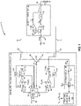
- FIG. 1 is a schematic diagram of a power amplifier system 10 that in accordance with the present disclosure includes a Doherty power amplifier (PA) 12 and envelope tracking (ET) circuitry 14.
- PA Doherty power amplifier
- ET envelope tracking circuitry 14
- the envelope tracking circuitry 14 is in the form of an ETIC.
- the Doherty PA 12 has a carrier amplifier 16 having a first supply node 18 and a peaking amplifier 20 having a second supply node 22.
- the Doherty PA 12 has a radio frequency (RF) signal input 24 that couples an RF signal 26 to the carrier amplifier 16 and the peaking amplifier 20.
- the RF signal 26 passes through a first impedance inverter 28 denoted "Ka" before reaching the peaking amplifier 20.
- the carrier amplifier 16 generates a main current signal I M that passes through a second impedance inverter 30 before reaching an RF output 32.
- the peaking amplifier 20 generates a peaking current signal j*lp that combines in-phase with the main current signal I M before being output through the RF output 32.
- a load R L is coupled between the RF output 32 and a fixed voltage node such as ground.
- the load R L is typically an antenna through which an amplified version of the RF signal 26 is transmitted.
- a single tracker circuit 34 of the ET circuitry 14 supplies power to the Doherty amplifier 12.
- the single tracker circuit 34 is configured to generate two modulated Vcc supply voltages, Vcc and Vccaux.
- a micro-charge-pump (MCP) 36 has an output coupled to a first supply output 38 through a power inductor 40.
- the MCP 36 is energized by a battery voltage V BAT .
- the first supply node 18 is coupled to the first supply output 38 to supply power the carrier amplifier 16.
- the ET circuitry 14 also includes a first tracking amplifier 42 coupled to the first supply output 38 by way of a relatively large capacitance ( ⁇ 2.2 ⁇ F) of a first offset capacitor 44.
- a first offset voltage V OFFA is present across the first offset capacitor 44 during operation.
- a first feedback (FB) network 46 is coupled between the first supply output 38 and a first tracking input 48 of the first tracking amplifier 42.
- the ET circuitry 14 also includes a second tracking amplifier 50 coupled to a second supply output 52 by way of a relatively small capacitance ( ⁇ 10 nF) of a second offset capacitor 54.
- a second offset voltage V OFFB is present across the second offset capacitor 54 during operation.
- a second feedback (FB) network 56 is coupled between the second supply output 52 and a second tracking input 58 of the second tracking amplifier 50.
- the second supply node 22 is coupled to the second supply output 52 to supply power the peaking amplifier 20.
- a tracking amplifiers supply 60 generates a first tracking amplifier supply voltage V SUPA that energizes the first tracking amplifier 42.
- the tracking amplifiers supply 60 also generates a second tracking amplifier supply voltage V SUPB that energizes the second tracking amplifier 50.
- the MCP 36 may supply a direct current voltage that the tracking amplifiers supply 60 uses to generate the first tracking amplifier supply voltage V SUPA and second tracking amplifier supply voltage V SUPB .
- a field effect transistor (FET) 62 has a first current terminal 64 coupled to the first supply node 18 through the first output 38.
- the FET 62 also has a second current terminal 66 coupled to the second supply node 22 through the second supply output 52.
- a control terminal 68 is used to control the FET 62.
- a control circuit 70 has a control output 72 coupled to the control terminal 68, wherein the control circuit 70 is configured to control the FET 62 to behave as a current source in a linear mode or as a closed switch or as an open switch.
- the control circuit 70 includes a digital processor configured to read values from look-up tables, apply the values to digital-to-analog converters, and read signal values from analog-to-digital converters.
- the control circuit 70 has a first sense input 74 coupled to a tracking output 76 of the second tracking amplifier 50 and a second sense input 78 coupled to the second supply output 52.
- a differential sensed voltage between the first sense input 74 and the second sense input 78 is equal to the second offset voltage V OFFB .
- An external transceiver produces a target Vramp modulation signal V TGT(t) that is received at a Vramp input 80 of the control circuit 70.
- the control circuit 70 is configured to respond to the target Vramp modulation signal V TGT(t) by simultaneously generating a first target signal V TGTA(t) at a first target signal output 82 and a second target signal V TGTB(t) at a second target signal output 84.
- the first target signal V TGTA(t) and the second target V TGTB(t) can have different amplitude shapes and different time alignment relative to each other.
- the first target signal output 82 is coupled to a first target signal input 86 of the first tracking amplifier 42.
- the first tracking amplifier 42 In response, the first tracking amplifier 42 generates a first tracking amplifier signal V AMPA(t) .
- the second target signal output 84 is coupled to a second target signal input 88 of the second tracking amplifier 50.
- the second tracking amplifier 50 generates a second tracking amplifier signal V AMPB(t) .
- Both the first supply voltage Vcc and the second supply voltage Vccaux track the first tracking amplifier signal V AMPA(t) and the second tracking amplifier signal V AMPB(t) .
- the envelope of the RF voltage across the carrier amplifier 16 is called Vm and the associated current is denoted I M .
- the envelope of the RF voltage across the peaking amplifier is called Vp and the associated current is denoted j*lp, where j is the imaginary component showing a 90 degree phase difference between the peaking current Ip and the main current I M .
- j is the imaginary component showing a 90 degree phase difference between the peaking current Ip and the main current I M .
- Figures 2A and 2B show various currents and voltages in the case of the Doherty amplifier 12 being in operation using the D 2 E method in which the peaking amplifier 20 is activated much lower than the -6 dB point relative to the peak envelope; that is, the Doherty operation of load-line modulation terminates or expires well below the peak envelope power and then both the carrier and peaking amplifiers each deliver half of the power between point B and point C.
- the average point of the modulation does not necessary fall at point A but can fall in between where the load modulation already has reduced the maximum impedance seen by the carrier amplifier at point A', thus reducing the load modulation efficiency enhancement and thus taking advantage of having envelope tracking on the carrier amplifier 16 to recover efficiency versus an ideal Doherty amplifier.
- the peaking amplifier 20 sees different modulation RF voltages when it is activated and can therefore take advantage of having a separate ET modulation on the peaking amplifier 20.
- the voltage seen by the peaking amplifier 20 at point A is equal to about one half of the voltage seen by the carrier amplifier 16 at point A, and the voltage seen by the peaking amplifier 20 at point B is equal to the same voltage seen by the carrier amplifier 16 at point B, which is twice the voltage at the peaking amplifier 20 at point A.
- Voltage seen by the carrier amplifier 16 from point B to point C is similar to the voltage seen by the carrier amplifier 20 at these points.
- Figure 3 shows the modulated Vcc voltages for the carrier amplifier 16 and peaking amplifier 20, where the modulation voltage swing of Vcc_peaking expected by the peaking amplifier is about Vccmax/2 to Vccmax.
- the Doherty amplifier 12 being operated as a barely Doherty power amplifier, the modulation voltages change since the load modulation is activated early in time and expires before the peak envelope of the RF modulation is reached.
- the modulation of the supply voltage Vcc on the peaking amplifier 20 has a lower dynamic range versus the modulation of the supply voltage Vcc of the carrier amplifier 16. This is because the minimum voltage is roughly a voltage equal to Vccm0/2 depicted in Figure 4 .
- the second offset capacitor 54 can be pre-charged to a value near Vccm0/2 to supply the second tracking amplifier 50 that drives the supply of the peaking amplifier 20 from a lower voltage supply for improved efficiency.
- Two separate Vcc modulation voltages Vcc_carrier(t) ⁇ Vcc_peaking(t) allow different load-line conversions and/or two different impedance inverter ratios on each of the carrier amplifier 16 and the peaking amplifier 20. As a result of this flexibility, power efficiency may be maximized.
- the carrier supply modulation Vcc_carrier(t) can be adjusted in proportion to values stored in an envelope tracking look-up table (ET-LUT) that provides isometric gain operation of the carrier amplifier 16.
- E-LUT envelope tracking look-up table
- the peaking supply modulation Vcc_peaking(t) can have another ET-LUT relation relative to the carrier supply modulation Vcc_carrier that allows isometric gain operation of the peaking amplifier 20, such that the overall gain of the Doherty amplifier 12 is linearized by taking advantage of the available two modulated supplies.
- Vcc_peaking ET-LUT change relative to the ET-LUT relation vs Vcc_carrier can be implemented inside the ET circuitry 14 directly, which uses the input modulated Vramp signal that is used by the Vcc_carrier as target and modifies this via a built-in mapping change to create another target signal for the Vcc_peaking, as shown in Figure 1 .
- Figure 5 illustrates the efficiency improvements expected, below point A, between the two peaking points A and B, and above point B.
- the efficiency of the carrier amplifier 16 is good, given the high load line seen in point A and still some good efficiency at point A', although the load line had dropped at point A' due to the barely operation but is improved due to the modulated supply ET operation of the Vcc_carrier between point A and point C to keep operating near compression.
- the efficiency of the peaking amplifier 20 is good, but the difference between (Vm(t) - Vp(t)), which represents the voltage across the FET element between Vcc(t) and Vccaux(t) of the ETIC, is dissipating the power for the modulated peaking current that flows through this FET, thus providing the equivalent of having the peaking amplifier supplied from Vccm0 voltage all the time between point A and point B.
- the peaking amplifier 20 is biased with a lower supply Vccmin_peaking at the start, where the peaking amplifier is activated and the control of the Vcc_peaking voltage allows better control the RF performances of the peaking amplifier 20 and assigns better bias control at the gate/base and the collector (not shown) versus only bias control on the gate/base of the RF transistors (not shown).
- the minimum Vcc for the Vcc_peaking can be different from the minimum Vcc_carrier if this helps to better optimize the behavior of the peaking amplifier 20 when it starts or stops to source RF current.
- the minimum Vcc can also be around half of the Vcc_carrier voltage at the transition point where the peaking amplifier 20 is engaged given that Vp envelope is one half of the Vm envelope. Indirectly, the carrier amplifier 16 and the peaking amplifier 20 can be linearized since each has its own modulated Vcc waveforms that are adjust by values from each ET-LUT.
- the carrier amplifier modulated supply voltage Vcc_carrier (t) is always greater than or equal to the peaking amplifier modulated supply voltage Vcc_peaking (t).
- the embodiments of the present disclosure are configured for the DiVeRT approach where Vcc(t) ⁇ Vccaux(t) is required.
- the carrier amplifier modulated supply voltage Vcc_carrier (t) has a low peak-to-average ratio and a lower peak-to-minimum voltage ratio.
- the tracker amplifier supply voltage V SUPA for the first tracking amplifier 42 may be lower, which increases the energy efficiency of the envelope tracker circuitry 14.
- the peaking amplifier modulated supply voltage Vcc_peaking (t) for the peaking amplifier 20 has a reduced peak-to-mininum voltage ratio swing. The presence of two different voltages V SUPA less than V SUPB used to differently supply the the first tracking amplifier 42 and the second tracking amplifier 20, respectively, provides for the maximum energy efficiency for the ET circuitry 14.
- Each power amplifier stage can be biased in class-AB and take advantage of ET amplitude modulation-amplitude modulation linearization of each amplifier via the respective supply path.
Landscapes
- Engineering & Computer Science (AREA)
- Power Engineering (AREA)
- Amplifiers (AREA)
Abstract
Description
- The present disclosure relates generally to radio frequency transmitters and, more particularly, to envelope tracking circuits that control Doherty-type power amplifiers within radio frequency transmitters.
- Mobile communication devices have become increasingly common in current society for providing wireless communication services. The prevalence of these mobile communication devices is driven in part by the many functions that are now enabled on such devices. Increased processing capabilities in such devices means that mobile communication devices have evolved from being pure communication tools into sophisticated mobile multimedia centers that enable enhanced user experiences.
- The redefined user experience requires higher data rates offered by wireless communication technologies, such as wireless fidelity (Wi-Fi), long-term evolution (LTE), and fifth-generation new-radio (5G-NR). To achieve the higher data rates in mobile communication devices, sophisticated power amplifiers may be employed to increase output power of radio frequency (RF) signals (e.g., maintaining sufficient energy per bit) communicated by mobile communication devices.
- Various power amplifier arrangements have been proposed and implemented in transmitter chains within the mobile communication devices to provide the desired output power while also meeting the power level control requirements of 5G-NR. One such power amplifier arrangement is the Doherty amplifier, which uses a carrier amplifier to operate at voltages up to the average power and uses the carrier amplifier and a peaking amplifier to operate at voltages between the average power and a peak power. While the Doherty amplifier provides options for providing power amplification, there remains room for improved energy efficiency and linearity during power amplification.
- A power amplifier system having a carrier amplifier having a first supply node, a peaking amplifier having a second supply node, and envelope tracking (ET) circuitry is disclosed. The ET circuitry has a first tracking amplifier that generates a first voltage signal at the first supply node, a second tracking amplifier that generates a second voltage signal at the second supply node, and a transistor coupled between the first supply node and the second supply node and a control input terminal. The first tracking amplifier and the second tracking amplifiers may also be referred to as parallel amplifiers. A control circuit has a first input coupled to an output of both or either of the first tracking amplifier and the second tracking amplifier and a control output terminal coupled to a control input terminal of the transistor, wherein the control circuit is configured to progressively turn on the transistor to pass current from the first supply node to the second supply node as the peaking amplifier progressively becomes active.
- Preferably, the ET circuitry is integrated into an ET integrated circuit, (ETIC).
- Preferably, the transistor is a field-effect transistor.
- This disclosure relates to envelope tracking operation with barely Doherty power amplifiers for additional enhanced transmitter efficiency, where a barely Doherty amplifier shows an increase of about 5% extra power-added efficiency versus average power tracking amplifiers, and where the combined barely Doherty with envelope tracking shows about +18% extra power-added efficiency versus average power tracking amplifiers.
- In another aspect, any of the foregoing aspects individually or together, and/or various separate aspects and features as described herein, may be combined for additional advantage. Any of the various features and elements as disclosed herein may be combined with one or more other disclosed features and elements unless indicated to the contrary herein.
- Those skilled in the art will appreciate the scope of the present disclosure and realize additional aspects thereof after reading the following detailed description of the preferred embodiments in association with the accompanying drawing figures.
- The accompanying drawing figures incorporated in and forming a part of this specification illustrate several aspects of the disclosure and, together with the description, serve to explain the principles of the disclosure.
-
Figure 1 is a schematic diagram of a power amplifier system that includes envelope tracking circuitry that is configured in accordance with the present disclosure to generate two modulated supply voltages from a single tracker circuit that energizes a Doherty power amplifier. -
Figure 2A is a graph showing peaking current of the peaking amplifier versus main current of the carrier amplifier for the Doherty amplifier ofFigure 1 . -
Figure 2B is a graph showing voltages for the peaking amplifier and the carrier amplifier versus carrier amplifier current for the Doherty amplifier ofFigure 1 . -
Figure 3 is a graph showing power supply voltage (Vcc) carrier and Vcc peaking swings for an Ideal Doherty amplifier. -
Figure 4 is a graph showing Vcc carrier and Vcc peaking swings for the Doherty amplifier ofFigure 1 . -
FIG. 5 is a graph illustrating efficiency improvements provided by the power amplifier system of the present disclosure. - The embodiments set forth below represent the necessary information to enable those skilled in the art to practice the embodiments and illustrate the best mode of practicing the embodiments. Upon reading the following description in light of the accompanying drawing figures, those skilled in the art will understand the concepts of the disclosure and will recognize applications of these concepts not particularly addressed herein. It should be understood that these concepts and applications fall within the scope of the disclosure and the accompanying claims.
- It will be understood that, although the terms first, second, etc. may be used herein to describe various elements, these elements should not be limited by these terms. These terms are only used to distinguish one element from another. For example, a first element could be termed a second element, and, similarly, a second element could be termed a first element, without departing from the scope of the present disclosure. As used herein, the term "and/or" includes any and all combinations of one or more of the associated listed items.
- It will be understood that when an element such as a layer, region, or substrate is referred to as being "on" or extending "onto" another element, it can be directly on or extend directly onto the other element or intervening elements may also be present. In contrast, when an element is referred to as being "directly on" or extending "directly onto" another element, there are no intervening elements present. Likewise, it will be understood that when an element such as a layer, region, or substrate is referred to as being "over" or extending "over" another element, it can be directly over or extend directly over the other element or intervening elements may also be present. In contrast, when an element is referred to as being "directly over" or extending "directly over" another element, there are no intervening elements present. It will also be understood that when an element is referred to as being "connected" or "coupled" to another element, it can be directly connected or coupled to the other element or intervening elements may be present. In contrast, when an element is referred to as being "directly connected" or "directly coupled" to another element, there are no intervening elements present.
- Relative terms such as "below" or "above" or "upper" or "lower" or "horizontal" or "vertical" may be used herein to describe a relationship of one element, layer, or region to another element, layer, or region as illustrated in the Figures. It will be understood that these terms and those discussed above are intended to encompass different orientations of the device in addition to the orientation depicted in the Figures.
- The terminology used herein is for the purpose of describing particular embodiments only and is not intended to be limiting of the disclosure. As used herein, the singular forms "a," "an," and "the" are intended to include the plural forms as well, unless the context clearly indicates otherwise. It will be further understood that the terms "comprises," "comprising," "includes," and/or "including" when used herein specify the presence of stated features, integers, steps, operations, elements, and/or components, but do not preclude the presence or addition of one or more other features, integers, steps, operations, elements, components, and/or groups thereof.
- Unless otherwise defined, all terms (including technical and scientific terms) used herein have the same meaning as commonly understood by one of ordinary skill in the art to which this disclosure belongs. It will be further understood that terms used herein should be interpreted as having a meaning that is consistent with their meaning in the context of this specification and the relevant art and will not be interpreted in an idealized or overly formal sense unless expressly so defined herein.
- Embodiments are described herein with reference to schematic illustrations of embodiments of the disclosure. As such, the actual dimensions of the layers and elements can be different, and variations from the shapes of the illustrations as a result, for example, of manufacturing techniques and/or tolerances, are expected. For example, a region illustrated or described as square or rectangular can have rounded or curved features, and regions shown as straight lines may have some irregularity. Thus, the regions illustrated in the figures are schematic and their shapes are not intended to illustrate the precise shape of a region of a device and are not intended to limit the scope of the disclosure. Additionally, sizes of structures or regions may be exaggerated relative to other structures or regions for illustrative purposes and, thus, are provided to illustrate the general structures of the present subject matter and may or may not be drawn to scale. Common elements between figures may be shown herein with common element numbers and may not be subsequently re-described.
- The present disclosure relates to envelope tracking integrated circuits (ETICs) with an approach referred to as DiVeRT, which stands for Dual instantaneous Voltage enhanced Rapid Tracking, which creates two simultaneous modulated power supply voltages from a single tracker circuit and thus enables new power amplifier topologies of modulating the collector of power amplifiers.
- Separately modulating the driver stage from the final output stages of power amplifiers allows wide modulation bandwidth ET such as ET 200 MHz, where the modulation of the first driver stage has the corresponding Vcc time-aligned to the radio frequency (RF) envelope and where the modulation of the final stages has the corresponding Vcc time-aligned to the RF envelope, which usually is slightly delayed by interstage networks.
- Separately modulating the carrier amplifier stages and the peaking amplifier stages for a barely Doherty (or load modulation) power amplifier, that is, the separate envelope tracking of carrier and peaking amplifiers, enables additional bias control of these two amplifier stages almost for free and minimizes degradation due to turn-on or turn-off of the peaking amplifier and enhances efficiency in addition to the load modulation itself and recovers the efficiency drop due to the use of barely Doherty approach. This is called D2E, which stands for Doherty and dual ET method in accordance with the present disclosure.
- Modulating two power amplifiers used in transmit (TX) diversity transmitting at either similar power or at different power levels the same RF modulation signal allows operation with a traditional approach of modulating both driver and final output stages of power amplifiers in different modes of ET, such as ProET (progressive Voffset (e) envelope tracking) or normal ET, or of average power tracking (APT), or APeT, which stands for operating in ET while using the APT controller with a tracking amplifier disabled.
-
Figure 1 is a schematic diagram of apower amplifier system 10 that in accordance with the present disclosure includes a Doherty power amplifier (PA) 12 and envelope tracking (ET)circuitry 14. In the exemplary embodiment ofFigure 1 , theenvelope tracking circuitry 14 is in the form of an ETIC. - The Doherty PA 12 has a
carrier amplifier 16 having afirst supply node 18 and a peakingamplifier 20 having asecond supply node 22. TheDoherty PA 12 has a radio frequency (RF)signal input 24 that couples anRF signal 26 to thecarrier amplifier 16 and the peakingamplifier 20. However, theRF signal 26 passes through afirst impedance inverter 28 denoted "Ka" before reaching the peakingamplifier 20. In operation, thecarrier amplifier 16 generates a main current signal IM that passes through asecond impedance inverter 30 before reaching anRF output 32. The peakingamplifier 20 generates a peaking current signal j*lp that combines in-phase with the main current signal IM before being output through theRF output 32. A load RL is coupled between theRF output 32 and a fixed voltage node such as ground. The load RL is typically an antenna through which an amplified version of theRF signal 26 is transmitted. - A
single tracker circuit 34 of theET circuitry 14 supplies power to theDoherty amplifier 12. Thesingle tracker circuit 34 is configured to generate two modulated Vcc supply voltages, Vcc and Vccaux. A micro-charge-pump (MCP) 36 has an output coupled to afirst supply output 38 through apower inductor 40. TheMCP 36 is energized by a battery voltage VBAT. Thefirst supply node 18 is coupled to thefirst supply output 38 to supply power thecarrier amplifier 16. - The
ET circuitry 14 also includes afirst tracking amplifier 42 coupled to thefirst supply output 38 by way of a relatively large capacitance (∼ 2.2 µF) of a first offsetcapacitor 44. A first offset voltage VOFFA is present across the first offsetcapacitor 44 during operation. A first feedback (FB)network 46 is coupled between thefirst supply output 38 and afirst tracking input 48 of thefirst tracking amplifier 42. - The
ET circuitry 14 also includes asecond tracking amplifier 50 coupled to asecond supply output 52 by way of a relatively small capacitance (∼ 10 nF) of a second offsetcapacitor 54. A second offset voltage VOFFB is present across the second offsetcapacitor 54 during operation. A second feedback (FB)network 56 is coupled between thesecond supply output 52 and asecond tracking input 58 of thesecond tracking amplifier 50. Thesecond supply node 22 is coupled to thesecond supply output 52 to supply power the peakingamplifier 20. - A tracking
amplifiers supply 60 generates a first tracking amplifier supply voltage VSUPA that energizes thefirst tracking amplifier 42. The trackingamplifiers supply 60 also generates a second tracking amplifier supply voltage VSUPB that energizes thesecond tracking amplifier 50. In some embodiments, theMCP 36 may supply a direct current voltage that the trackingamplifiers supply 60 uses to generate the first tracking amplifier supply voltage VSUPA and second tracking amplifier supply voltage VSUPB. - A field effect transistor (FET) 62 has a first
current terminal 64 coupled to thefirst supply node 18 through thefirst output 38. TheFET 62 also has a secondcurrent terminal 66 coupled to thesecond supply node 22 through thesecond supply output 52. Acontrol terminal 68 is used to control theFET 62. Acontrol circuit 70 has acontrol output 72 coupled to thecontrol terminal 68, wherein thecontrol circuit 70 is configured to control theFET 62 to behave as a current source in a linear mode or as a closed switch or as an open switch. In at least some embodiments, thecontrol circuit 70 includes a digital processor configured to read values from look-up tables, apply the values to digital-to-analog converters, and read signal values from analog-to-digital converters. In the exemplary embodiment ofFigure 1 , thecontrol circuit 70 has afirst sense input 74 coupled to a trackingoutput 76 of thesecond tracking amplifier 50 and asecond sense input 78 coupled to thesecond supply output 52. A differential sensed voltage between thefirst sense input 74 and thesecond sense input 78 is equal to the second offset voltage VOFFB. - An external transceiver produces a target Vramp modulation signal VTGT(t) that is received at a
Vramp input 80 of thecontrol circuit 70. Thecontrol circuit 70 is configured to respond to the target Vramp modulation signal VTGT(t) by simultaneously generating a first target signal VTGTA(t) at a firsttarget signal output 82 and a second target signal VTGTB(t) at a secondtarget signal output 84. The first target signal VTGTA(t) and the second target VTGTB(t) can have different amplitude shapes and different time alignment relative to each other. The firsttarget signal output 82 is coupled to a firsttarget signal input 86 of thefirst tracking amplifier 42. In response, thefirst tracking amplifier 42 generates a first tracking amplifier signal VAMPA(t). The secondtarget signal output 84 is coupled to a secondtarget signal input 88 of thesecond tracking amplifier 50. In response, thesecond tracking amplifier 50 generates a second tracking amplifier signal VAMPB(t). Both the first supply voltage Vcc and the second supply voltage Vccaux track the first tracking amplifier signal VAMPA(t) and the second tracking amplifier signal VAMPB(t). - During operation of the
Doherty amplifier 12, the envelope of the RF voltage across thecarrier amplifier 16 is called Vm and the associated current is denoted IM. The envelope of the RF voltage across the peaking amplifier is called Vp and the associated current is denoted j*lp, where j is the imaginary component showing a 90 degree phase difference between the peaking current Ip and the main current IM. Moreover, for theDoherty amplifier 12 is operated as a barely Doherty power amplifier with assumptions that the load-line transformations are not necessarily the same between the two amplifier stages. -
Figures 2A and2B show various currents and voltages in the case of theDoherty amplifier 12 being in operation using the D2E method in which the peakingamplifier 20 is activated much lower than the -6 dB point relative to the peak envelope; that is, the Doherty operation of load-line modulation terminates or expires well below the peak envelope power and then both the carrier and peaking amplifiers each deliver half of the power between point B and point C. - The average point of the modulation does not necessary fall at point A but can fall in between where the load modulation already has reduced the maximum impedance seen by the carrier amplifier at point A', thus reducing the load modulation efficiency enhancement and thus taking advantage of having envelope tracking on the
carrier amplifier 16 to recover efficiency versus an ideal Doherty amplifier. - The peaking
amplifier 20 sees different modulation RF voltages when it is activated and can therefore take advantage of having a separate ET modulation on the peakingamplifier 20. The voltage seen by the peakingamplifier 20 at point A is equal to about one half of the voltage seen by thecarrier amplifier 16 at point A, and the voltage seen by the peakingamplifier 20 at point B is equal to the same voltage seen by thecarrier amplifier 16 at point B, which is twice the voltage at the peakingamplifier 20 at point A. Voltage seen by thecarrier amplifier 16 from point B to point C is similar to the voltage seen by thecarrier amplifier 20 at these points. - In the case of a modulation signal of peak-to-average ratio of 6 dB and an ideal Doherty case,
Figure 3 shows the modulated Vcc voltages for thecarrier amplifier 16 and peakingamplifier 20, where the modulation voltage swing of Vcc_peaking expected by the peaking amplifier is about Vccmax/2 to Vccmax. In the case of theDoherty amplifier 12 being operated as a barely Doherty power amplifier, the modulation voltages change since the load modulation is activated early in time and expires before the peak envelope of the RF modulation is reached. - As shown in
Figure 4 , the modulation of the supply voltage Vcc on the peakingamplifier 20 has a lower dynamic range versus the modulation of the supply voltage Vcc of thecarrier amplifier 16. This is because the minimum voltage is roughly a voltage equal to Vccm0/2 depicted inFigure 4 . Thus, the second offsetcapacitor 54 can be pre-charged to a value near Vccm0/2 to supply thesecond tracking amplifier 50 that drives the supply of the peakingamplifier 20 from a lower voltage supply for improved efficiency. Two separate Vcc modulation voltages Vcc_carrier(t) ≥ Vcc_peaking(t) allow different load-line conversions and/or two different impedance inverter ratios on each of thecarrier amplifier 16 and the peakingamplifier 20. As a result of this flexibility, power efficiency may be maximized. - There may be different linearizations by way of the different supply voltages for the
carrier amplifier 16 and the peakingamplifier 20 to maximize the overall linearity of theDoherty amplifier 12. For example, the carrier supply modulation Vcc_carrier(t) can be adjusted in proportion to values stored in an envelope tracking look-up table (ET-LUT) that provides isometric gain operation of thecarrier amplifier 16. the peaking supply modulation Vcc_peaking(t) can have another ET-LUT relation relative to the carrier supply modulation Vcc_carrier that allows isometric gain operation of the peakingamplifier 20, such that the overall gain of theDoherty amplifier 12 is linearized by taking advantage of the available two modulated supplies. The Vcc_peaking ET-LUT change relative to the ET-LUT relation vs Vcc_carrier can be implemented inside theET circuitry 14 directly, which uses the input modulated Vramp signal that is used by the Vcc_carrier as target and modifies this via a built-in mapping change to create another target signal for the Vcc_peaking, as shown inFigure 1 . -
Figure 5 illustrates the efficiency improvements expected, below point A, between the two peaking points A and B, and above point B. The efficiency of thecarrier amplifier 16 is good, given the high load line seen in point A and still some good efficiency at point A', although the load line had dropped at point A' due to the barely operation but is improved due to the modulated supply ET operation of the Vcc_carrier between point A and point C to keep operating near compression. - The efficiency of the peaking
amplifier 20 is good, but the difference between (Vm(t) - Vp(t)), which represents the voltage across the FET element between Vcc(t) and Vccaux(t) of the ETIC, is dissipating the power for the modulated peaking current that flows through this FET, thus providing the equivalent of having the peaking amplifier supplied from Vccm0 voltage all the time between point A and point B. - The peaking
amplifier 20 is biased with a lower supply Vccmin_peaking at the start, where the peaking amplifier is activated and the control of the Vcc_peaking voltage allows better control the RF performances of the peakingamplifier 20 and assigns better bias control at the gate/base and the collector (not shown) versus only bias control on the gate/base of the RF transistors (not shown). The minimum Vcc for the Vcc_peaking can be different from the minimum Vcc_carrier if this helps to better optimize the behavior of the peakingamplifier 20 when it starts or stops to source RF current. The minimum Vcc can also be around half of the Vcc_carrier voltage at the transition point where the peakingamplifier 20 is engaged given that Vp envelope is one half of the Vm envelope. Indirectly, thecarrier amplifier 16 and the peakingamplifier 20 can be linearized since each has its own modulated Vcc waveforms that are adjust by values from each ET-LUT. - Note that in embodiments of the present disclosure, the carrier amplifier modulated supply voltage Vcc_carrier (t) is always greater than or equal to the peaking amplifier modulated supply voltage Vcc_peaking (t). Thus, the embodiments of the present disclosure are configured for the DiVeRT approach where Vcc(t) ≥ Vccaux(t) is required.
- Furthermore, the the carrier amplifier modulated supply voltage Vcc_carrier (t) has a low peak-to-average ratio and a lower peak-to-minimum voltage ratio. Thus, the tracker amplifier supply voltage VSUPA for the
first tracking amplifier 42 may be lower, which increases the energy efficiency of theenvelope tracker circuitry 14. Moreover, the peaking amplifier modulated supply voltage Vcc_peaking (t) for the peakingamplifier 20 has a reduced peak-to-mininum voltage ratio swing. The presence of two different voltages VSUPA less than VSUPB used to differently supply the thefirst tracking amplifier 42 and thesecond tracking amplifier 20, respectively, provides for the maximum energy efficiency for theET circuitry 14. - There may be a mix and match of different power amplifier topologies using Vcc and Vccaux supply voltages. Further, there may be different time alignment between the Vcc_carrier(t) and Vcc_peaking(t), if there is any mismatch in time between the two RF envelopes at each power amplifier. Each power amplifier stage can be biased in class-AB and take advantage of ET amplitude modulation-amplitude modulation linearization of each amplifier via the respective supply path.
- It is contemplated that any of the foregoing aspects, and/or various separate aspects and features as described herein, may be combined for additional advantage. Any of the various embodiments as disclosed herein may be combined with one or more other disclosed embodiments unless indicated to the contrary herein.
Claims (15)
- A power amplifier system comprising:a carrier amplifier having a first supply node;a peaking amplifier having a second supply node; and
envelope tracking, ET, circuitry comprising:a first tracking amplifier configured to generate a first voltage signal at the first supply node;a second tracking amplifier configured to generate a second voltage signal at the second supply node;a transistor having a first current terminal coupled the first supply node and a second current terminal coupled to the second supply node; anda control circuit having a first input coupled to an output of both or either of the first tracking amplifier and the second tracking amplifier and a control output terminal coupled to a control input terminal of the transistor, wherein the control circuit is configured to progressively turn on the transistor to pass current from the first supply node to the second supply node as the peaking amplifier progressively becomes active. - The power amplifier system of claim 1 wherein the control circuit determines that the peaking amplifier is becoming increasingly active by monitoring a tracking output voltage at the first input of the control circuit.
- The power amplifier system of claim 2 wherein the control circuit has a second input coupled to the second node to monitor voltage at the second node.
- The power amplifier system of claim 3 wherein the control circuit is configured to monitor a differential voltage between the first input and the second input and in response progressively turn on the transistor to pass current from the first supply node to the second node as the peaking amplifier progressively becomes active.
- The power amplifier system of claim 1 wherein the first supply signal has a first amplitude modulation that follows the envelope of a radio frequency signal received by the ET circuitry and the second supply signal has a second amplitude modulation that follows the envelope of the radio frequency signal received by the ET circuitry.
- The power amplifier system of claim 1 wherein the control circuit is configured to cause a rate of change of peaking current supplying the peaking amplifier with to be greater than a rate of change of carrier current supplying the carrier amplifier until the carrier current and the peaking current are substantially equal, and wherein the rate of change of peaking current supplying the peaking amplifier preferably has a slope that is at least twice a slope of the rate of change of the carrier current supplying the carrier amplifier.
- The power amplifier system of claim 1 wherein the ET circuitry is configured to ensure that a voltage at the first supply node supplying the carrier amplifier is remains greater than or equal to the voltage at the second supply node supplying the peaking amplifier.
- The power amplifier system of claim 1 wherein the ET circuitry further comprises a tracker circuit having a micro-charge-pump with an output coupled to the first supply node through a power inductor.
- The power amplifier system of claim 1 wherein the carrier amplifier and the peaking amplifier are coupled in a Doherty amplifier configuration.
- The power amplifier system of claim 9 further comprising a first impedance inverter coupled between a signal output of the carrier amplifier and a signal output of the peaking amplifier.
- The power amplifier system of claim 10 further comprising a second impedance inverter coupled between a signal input of the carrier amplifier and a signal input of the peaking amplifier, and wherein the first impedance inverter and the second impedance inverter preferably have substantially different impedance inverter ratios.
- The power amplifier system of claim 1 further comprising a first capacitor is coupled between an output of first tracking amplifier and the first supply node.
- The power amplifier system of claim 12 further comprising a second capacitor coupled between an output of the second tracking amplifier and the second supply node, wherein capacitance of the second capacitor preferably is an order of magnitude less than capacitance of the first capacitor.
- The power amplifier system of claim 1 wherein the control circuit is further configured to adjust a supply voltage at the first supply node based on values stored in a first envelope tracking look-up table, ET-LUT, to provide isometric gain operation of the carrier amplifier.
- The power amplifier system of claim 1 or 14 wherein the control circuit is further configured to adjust a supply voltage at the second supply node based on values stored in a second ET-LUT to provide isometric gain operation of the peaking amplifier.
Applications Claiming Priority (2)
| Application Number | Priority Date | Filing Date | Title |
|---|---|---|---|
| US202163149556P | 2021-02-15 | 2021-02-15 | |
| US17/579,796 US12267046B2 (en) | 2021-02-15 | 2022-01-20 | Power amplifier system |
Publications (1)
| Publication Number | Publication Date |
|---|---|
| EP4044429A1 true EP4044429A1 (en) | 2022-08-17 |
Family
ID=80034922
Family Applications (1)
| Application Number | Title | Priority Date | Filing Date |
|---|---|---|---|
| EP22153526.3A Pending EP4044429A1 (en) | 2021-02-15 | 2022-01-26 | Power amplifier system |
Country Status (5)
| Country | Link |
|---|---|
| US (2) | US12267046B2 (en) |
| EP (1) | EP4044429A1 (en) |
| JP (1) | JP2022124466A (en) |
| KR (1) | KR20220117144A (en) |
| CN (1) | CN114944818A (en) |
Families Citing this family (6)
| Publication number | Priority date | Publication date | Assignee | Title |
|---|---|---|---|---|
| US11909385B2 (en) | 2020-10-19 | 2024-02-20 | Qorvo Us, Inc. | Fast-switching power management circuit and related apparatus |
| CN116458058A (en) | 2020-11-16 | 2023-07-18 | Qorvo美国公司 | Envelope tracking integrated circuit operable across wide modulation bandwidths |
| WO2022103496A1 (en) | 2020-11-16 | 2022-05-19 | Qorvo Us, Inc. | Power management circuit operable with multiple supply voltages |
| US12265442B2 (en) | 2020-12-04 | 2025-04-01 | Qorvo Us, Inc. | Power management integrated circuit |
| EP4475434A3 (en) | 2020-12-22 | 2025-03-05 | Qorvo US, Inc. | Power management apparatus operable with multiple configurations |
| US12063018B2 (en) | 2021-06-10 | 2024-08-13 | Qorvo Us, Inc. | Envelope tracking integrated circuit operable with multiple types of power amplifiers |
Citations (6)
| Publication number | Priority date | Publication date | Assignee | Title |
|---|---|---|---|---|
| US20060055458A1 (en) * | 2003-01-09 | 2006-03-16 | Nec Corporation | Doherty amplifier |
| US20080231358A1 (en) * | 2007-03-23 | 2008-09-25 | Mitsubishi Electric Corporation | Power amplifier circuit |
| US20170005619A1 (en) * | 2015-07-01 | 2017-01-05 | Qorvo Us, Inc. | Envelope tracking power converter circuitry |
| DE102019220150A1 (en) * | 2018-12-19 | 2020-06-25 | Qorvo Us, Inc. | Envelope tracking integrated circuit and related device |
| US20200321848A1 (en) * | 2019-04-02 | 2020-10-08 | Qorvo Us, Inc. | Dual-modulation power management circuit |
| WO2021016350A1 (en) * | 2019-07-25 | 2021-01-28 | Qorvo Us, Inc. | Multi-mode power management apparatus |
Family Cites Families (318)
| Publication number | Priority date | Publication date | Assignee | Title |
|---|---|---|---|---|
| FR2558317B1 (en) | 1984-01-13 | 1989-05-05 | Thomson Csf | HIGH PRECISION TUNABLE OSCILLATOR AND RADAR COMPRISING SUCH AN OSCILLATOR |
| US5266936A (en) | 1989-05-09 | 1993-11-30 | Nec Corporation | Driving circuit for liquid crystal display |
| JPH0654877B2 (en) | 1989-09-19 | 1994-07-20 | 日本電信電話株式会社 | Linear transmitter |
| CA2109755C (en) | 1993-11-23 | 2004-11-02 | John Barry French | Composite bridge amplifier with output overload and thermal protection |
| US5838732A (en) | 1994-10-31 | 1998-11-17 | Airnet Communications Corp. | Reducing peak-to-average variance of a composite transmitted signal generated by a digital combiner via carrier phase offset |
| US6107862A (en) | 1997-02-28 | 2000-08-22 | Seiko Instruments Inc. | Charge pump circuit |
| US6141541A (en) | 1997-12-31 | 2000-10-31 | Motorola, Inc. | Method, device, phone and base station for providing envelope-following for variable envelope radio frequency signals |
| US6141377A (en) | 1998-07-30 | 2000-10-31 | Cisco Technology, Inc. | Method and apparatus for voice frequency noise reduction in splitterless ADSL |
| JP3630228B2 (en) | 2000-08-16 | 2005-03-16 | インターナショナル・ビジネス・マシーンズ・コーポレーション | POWER SUPPLY DEVICE, BATTERY, ELECTRIC DEVICE, AND MEMORY EFFECT DETECTION METHOD |
| US6411531B1 (en) | 2000-11-21 | 2002-06-25 | Linear Technology Corporation | Charge pump DC/DC converters with reduced input noise |
| US7009858B2 (en) | 2001-01-29 | 2006-03-07 | Seiko Epson Corporation | Adjustable current consumption power supply apparatus |
| JP2002304434A (en) | 2001-04-06 | 2002-10-18 | Nec Corp | Method, apparatus and program for creating power supply model of semiconductor integrated circuit for EMI simulation |
| EP1310959B1 (en) | 2001-11-09 | 2008-06-18 | STMicroelectronics S.r.l. | Low power charge pump circuit |
| US7583754B2 (en) | 2002-10-31 | 2009-09-01 | Zte Corporation | Method and system for broadband predistortion linearization |
| US7432614B2 (en) | 2003-01-17 | 2008-10-07 | Hong Kong University Of Science And Technology | Single-inductor multiple-output switching converters in PCCM with freewheel switching |
| GB2398648B (en) | 2003-02-19 | 2005-11-09 | Nujira Ltd | Power supply stage for an amplifier |
| US6985033B1 (en) | 2003-05-15 | 2006-01-10 | Marvell International Ltd. | Circuits and methods for adjusting power amplifier predistortion, and power amplifiers and other devices including the same |
| US7043213B2 (en) | 2003-06-24 | 2006-05-09 | Northrop Grumman Corporation | Multi-mode amplifier system |
| US20050088160A1 (en) | 2003-09-19 | 2005-04-28 | Matsushita Electric Industrial Co., Ltd. | Multi output DC-DC converter |
| US7421254B2 (en) | 2003-10-23 | 2008-09-02 | Broadcom Corporation | High linearity, high efficiency power amplifier with DSP assisted linearity optimization |
| US7333582B2 (en) | 2004-03-02 | 2008-02-19 | Matsushita Electric Industrial Co., Ltd. | Two-point frequency modulation apparatus, wireless transmitting apparatus, and wireless receiving apparatus |
| US20050227646A1 (en) | 2004-03-18 | 2005-10-13 | Ryo Yamazaki | Detecting and maintaining linearity in a power amplifier system through comparing peak and RMS power levels |
| US7193467B2 (en) | 2004-03-30 | 2007-03-20 | Rambus Inc. | Differential amplifiers and methods of using same |
| US20060199553A1 (en) | 2005-03-07 | 2006-09-07 | Andrew Corporation | Integrated transceiver with envelope tracking |
| US7456621B2 (en) | 2005-05-06 | 2008-11-25 | Silicon Laboratories Inc. | Digital controller based power factor correction circuit |
| US20070053217A1 (en) | 2005-09-02 | 2007-03-08 | Lear Corporation | Converter for automotive use |
| JP2007074121A (en) | 2005-09-05 | 2007-03-22 | Fujitsu Ltd | Amplifier and mutual conductance control method |
| US7519336B2 (en) | 2006-05-05 | 2009-04-14 | Nokia Corporation | Method and arrangement for optimizing efficiency of a power amplifier |
| US7570931B2 (en) | 2006-06-02 | 2009-08-04 | Crestcom, Inc. | RF transmitter with variably biased RF power amplifier and method therefor |
| US7518445B2 (en) | 2006-06-04 | 2009-04-14 | Samsung Electro-Mechanics Company, Ltd. | Systems, methods, and apparatuses for linear envelope elimination and restoration transmitters |
| JP4369462B2 (en) | 2006-11-22 | 2009-11-18 | Okiセミコンダクタ株式会社 | Charge pump type DC / DC converter |
| US20080231115A1 (en) | 2007-03-16 | 2008-09-25 | Gyuha Cho | Multiple-Output DC-DC Converter |
| US7696735B2 (en) | 2007-03-30 | 2010-04-13 | Intel Corporation | Switched capacitor converters |
| US7471155B1 (en) | 2007-05-25 | 2008-12-30 | Rf Micro Devices, Inc. | Cancelling switching power supply ripple from a radio frequency signal |
| US7808220B2 (en) | 2007-07-11 | 2010-10-05 | Semtech Corporation | Method and apparatus for a charge pump DC-to-DC converter having parallel operating modes |
| US7949316B2 (en) | 2008-01-29 | 2011-05-24 | Panasonic Corporation | High-efficiency envelope tracking systems and methods for radio frequency power amplifiers |
| US20100019052A1 (en) | 2008-07-28 | 2010-01-28 | Yip Chiu Ming | Line voltage thermostat with energy measurement mechanism |
| US7859454B2 (en) | 2008-08-15 | 2010-12-28 | Broadcom Corporation | Method and system for calibrating group delay errors in a combined GPS and GLONASS receiver |
| WO2010020833A1 (en) | 2008-08-20 | 2010-02-25 | Freescale Semiconductor, Inc. | Wireless communication unit, integrated circuit and method of power control of a power amplifier therefor |
| JP5338262B2 (en) * | 2008-11-05 | 2013-11-13 | 日本電気株式会社 | Power amplifier and amplification method thereof |
| GB2530424B (en) | 2008-11-18 | 2016-05-04 | Nujira Ltd | Power Supply Arrangement For Multi-Stage Amplifier |
| JP6085406B2 (en) | 2008-12-02 | 2017-02-22 | サイプレス セミコンダクター コーポレーション | Output voltage control circuit, electronic device, and output voltage control method |
| US8232834B2 (en) | 2009-05-07 | 2012-07-31 | Analog Devices, Inc. | Boosting xDSL amplifier supply power on-demand |
| US8130042B2 (en) | 2009-06-03 | 2012-03-06 | Peregrine Semiconductor Corporation | Methods and devices for leakage current reduction |
| US8975879B2 (en) | 2009-09-14 | 2015-03-10 | Dialog Semiconductor Gmbh | Switching converter having a plurality N of outputs providing N output signals and at least one inductor and method for controlling such a switching converter |
| TWI422127B (en) | 2009-09-29 | 2014-01-01 | Richtek Technology Corp | Control circuit and method for a buck-boost power converter |
| US8509713B2 (en) | 2009-12-21 | 2013-08-13 | Ubidyne, Inc. | Single envelope tracking system for an active antenna array |
| JP2011172206A (en) | 2010-01-21 | 2011-09-01 | Panasonic Corp | High-frequency power amplifier and wireless communication device including the same |
| US8548398B2 (en) | 2010-02-01 | 2013-10-01 | Rf Micro Devices, Inc. | Envelope power supply calibration of a multi-mode radio frequency power amplifier |
| US7994862B1 (en) | 2010-02-11 | 2011-08-09 | Sige Semiconductor Inc. | Circuit and method of temperature dependent power amplifier biasing |
| GB2479579B (en) | 2010-04-15 | 2017-12-06 | Snaptrack Inc | Timing alignment for modulated supply |
| WO2011133542A1 (en) | 2010-04-19 | 2011-10-27 | Rf Micro Devices, Inc. | Pseudo-envelope following power management system |
| US8519788B2 (en) | 2010-04-19 | 2013-08-27 | Rf Micro Devices, Inc. | Boost charge-pump with fractional ratio and offset loop for supply modulation |
| US9008597B2 (en) | 2010-04-20 | 2015-04-14 | Rf Micro Devices, Inc. | Direct current (DC)-DC converter having a multi-stage output filter |
| US8731498B2 (en) | 2010-04-20 | 2014-05-20 | Rf Micro Devices, Inc. | Temperature correcting an envelope power supply signal for RF PA circuitry |
| US8942651B2 (en) | 2010-04-20 | 2015-01-27 | Rf Micro Devices, Inc. | Cascaded converged power amplifier |
| US8706063B2 (en) | 2010-04-20 | 2014-04-22 | Rf Micro Devices, Inc. | PA envelope power supply undershoot compensation |
| US9900204B2 (en) | 2010-04-20 | 2018-02-20 | Qorvo Us, Inc. | Multiple functional equivalence digital communications interface |
| US8174313B2 (en) | 2010-05-17 | 2012-05-08 | Avago Technologies Wireless Ip (Singapore) Pte. Ltd. | Apparatus and method for controlling power amplifier |
| GB2482738B (en) | 2010-08-13 | 2015-05-13 | Nujira Ltd | Switch mode power supply for envelope tracking |
| WO2012031241A2 (en) | 2010-09-03 | 2012-03-08 | Skyworks Solutions, Inc. | High-voltage tolerant voltage regulator |
| EP2432107B1 (en) | 2010-09-15 | 2013-10-23 | Nxp B.V. | Single-input multi-output DC-DC converter |
| US9172303B2 (en) | 2010-09-30 | 2015-10-27 | Stmicroelectronics International N.V. | Power management unit systems and methods |
| KR101743014B1 (en) | 2010-11-11 | 2017-06-02 | 삼성전자주식회사 | Apparatus and method for increasing output efficiency in mobile communication terminal |
| US8588713B2 (en) | 2011-01-10 | 2013-11-19 | Rf Micro Devices, Inc. | Power management system for multi-carriers transmitter |
| US8461928B2 (en) | 2011-01-25 | 2013-06-11 | Provigent Ltd. | Constant-gain power amplifier |
| US8803605B2 (en) | 2011-02-01 | 2014-08-12 | Mediatek Singapore Pte. Ltd. | Integrated circuit, wireless communication unit and method for providing a power supply |
| US8975960B2 (en) | 2011-02-01 | 2015-03-10 | Mediatek Singapore Pte. Ltd. | Integrated circuit wireless communication unit and method for providing a power supply |
| US9166538B2 (en) | 2011-02-01 | 2015-10-20 | Mediatek Singapore Pte. Ltd. | Integrated circuit wireless communication unit and method for providing a power supply |
| WO2012109161A2 (en) | 2011-02-07 | 2012-08-16 | Skyworks Solutions, Inc. | Apparatus and methods for envelope tracking calibration |
| US8624760B2 (en) | 2011-02-07 | 2014-01-07 | Rf Micro Devices, Inc. | Apparatuses and methods for rate conversion and fractional delay calculation using a coefficient look up table |
| US8723492B2 (en) | 2011-03-22 | 2014-05-13 | Integrated Device Technology, Inc. | Autonomous controlled headroom low dropout regulator for single inductor multiple output power supply |
| US8725218B2 (en) | 2011-03-25 | 2014-05-13 | R2 Semiconductor, Inc. | Multimode operation DC-DC converter |
| US8718188B2 (en) | 2011-04-25 | 2014-05-06 | Skyworks Solutions, Inc. | Apparatus and methods for envelope tracking |
| EP2518878B1 (en) | 2011-04-29 | 2018-10-17 | STMicroelectronics S.r.l. | DC-DC converter, method for operating the DC-DC converter, environmental energy harvesting system comprising the DC-DC converter, and apparatus comprising the energy harvesting system |
| US8774065B2 (en) | 2011-05-02 | 2014-07-08 | Rf Micro Devices, Inc. | Radio front end and power management architecture for LTE-advanced |
| US9246460B2 (en) | 2011-05-05 | 2016-01-26 | Rf Micro Devices, Inc. | Power management architecture for modulated and constant supply operation |
| WO2012151594A2 (en) | 2011-05-05 | 2012-11-08 | Rf Micro Devices, Inc. | Power managent system for pseudo-envelope and average power tracking |
| US9247496B2 (en) | 2011-05-05 | 2016-01-26 | Rf Micro Devices, Inc. | Power loop control based envelope tracking |
| US9379667B2 (en) | 2011-05-05 | 2016-06-28 | Rf Micro Devices, Inc. | Multiple power supply input parallel amplifier based envelope tracking |
| US9099919B2 (en) | 2011-05-09 | 2015-08-04 | The Hong Kong University Of Science And Technology | Single-inductor-multiple-output regulator with synchronized current mode hysteretic control |
| JP5637065B2 (en) | 2011-05-13 | 2014-12-10 | 住友電気工業株式会社 | Amplifier circuit and wireless communication device |
| US8879665B2 (en) | 2011-06-08 | 2014-11-04 | Broadcom Corporation | Controlling a power amplifier based on transmitter output emissions |
| GB2488380B (en) | 2011-06-24 | 2018-04-04 | Snaptrack Inc | Envelope tracking system for mimo |
| US9065334B2 (en) | 2011-06-27 | 2015-06-23 | Mediatek Inc. | Voltage converter having auxiliary switch implemented therein and related voltage converting method thereof |
| US9496828B2 (en) | 2011-07-22 | 2016-11-15 | Texas Instruments Incorporated | System and method for envelope tracking power supply |
| US9018921B2 (en) | 2011-08-17 | 2015-04-28 | National Semiconductor Corporation | Battery charger architecture |
| US8699247B2 (en) | 2011-09-09 | 2014-04-15 | Sandisk Technologies Inc. | Charge pump system dynamically reconfigurable for read and program |
| KR101821294B1 (en) | 2011-09-21 | 2018-01-23 | 삼성전자주식회사 | Apparatus and Method for Reduced Bandwidth Envelope Tracking and Corresponding Digital Pre-Distortion |
| KR20130043425A (en) | 2011-10-20 | 2013-04-30 | 삼성전자주식회사 | Digital pre-distortion method and apparatus for changing memory order according to input level |
| US8786371B2 (en) | 2011-11-18 | 2014-07-22 | Skyworks Solutions, Inc. | Apparatus and methods for voltage converters |
| US8868110B2 (en) | 2011-11-21 | 2014-10-21 | Broadcom Corporation | Wireless communication device capable of efficient network search |
| US9256234B2 (en) | 2011-12-01 | 2016-02-09 | Rf Micro Devices, Inc. | Voltage offset loop for a switching controller |
| US9280163B2 (en) | 2011-12-01 | 2016-03-08 | Rf Micro Devices, Inc. | Average power tracking controller |
| US9041364B2 (en) | 2011-12-01 | 2015-05-26 | Rf Micro Devices, Inc. | RF power converter |
| US8947161B2 (en) | 2011-12-01 | 2015-02-03 | Rf Micro Devices, Inc. | Linear amplifier power supply modulation for envelope tracking |
| US9041365B2 (en) | 2011-12-01 | 2015-05-26 | Rf Micro Devices, Inc. | Multiple mode RF power converter |
| US9490697B2 (en) | 2011-12-05 | 2016-11-08 | Freescale Semiconductor, Inc. | Self-bootstrap driving circuit and DC-DC converter |
| US8988054B2 (en) | 2011-12-27 | 2015-03-24 | St-Ericsson Sa | Single feedback loop for parallel architecture buck converter—LDO regulator |
| US9298198B2 (en) | 2011-12-28 | 2016-03-29 | Rf Micro Devices, Inc. | Noise reduction for envelope tracking |
| US20130176961A1 (en) | 2012-01-09 | 2013-07-11 | Qualcomm Incorporated | Apparatus and methods of unambiguous mac-i pdu formatting |
| GB2498392B (en) | 2012-01-16 | 2016-01-13 | Nujira Ltd | Crest factor reduction applied to shaping table to increase power amplifier efficency of envelope tracking amplifier |
| US8880012B2 (en) | 2012-01-19 | 2014-11-04 | Motorola Mobility Llc | Method and apparatus for resource block based transmitter optimization in wireless communication devices |
| CN104185953B (en) | 2012-02-09 | 2016-08-17 | 天工方案公司 | Apparatus and method for envelope-tracking |
| US9069365B2 (en) | 2012-02-18 | 2015-06-30 | R2 Semiconductor, Inc. | DC-DC converter enabling rapid output voltage changes |
| US9529375B2 (en) | 2012-02-28 | 2016-12-27 | Texas Instruments Deutschland Gmbh | Single inductor-multiple output DC-DC converter, method for operating the same and electronic device comprising the converter |
| KR102037551B1 (en) | 2012-03-04 | 2019-10-28 | 퀀탄스, 인코포레이티드 | Envelope tracking power amplifier system with delay calibration |
| US20130234692A1 (en) | 2012-03-07 | 2013-09-12 | Medtronic, Inc. | Voltage supply and method with two references having differing accuracy and power consumption |
| JP5880239B2 (en) | 2012-04-13 | 2016-03-08 | 株式会社ソシオネクスト | Power supply device and power supply control method |
| US8665016B2 (en) | 2012-04-30 | 2014-03-04 | Broadcom Corporation | Supply tracking |
| US8773200B2 (en) | 2012-07-08 | 2014-07-08 | R2 Semiconductor, Inc. | Decoupling circuits for filtering a voltage supply of multiple power amplifiers |
| US8896374B2 (en) | 2012-07-25 | 2014-11-25 | Qualcomm Incorporated | Energy source sharing |
| US9020451B2 (en) | 2012-07-26 | 2015-04-28 | Rf Micro Devices, Inc. | Programmable RF notch filter for envelope tracking |
| WO2014021318A1 (en) | 2012-08-01 | 2014-02-06 | 独立行政法人産業技術総合研究所 | Spectral envelope and group delay inference system and voice signal synthesis system for voice analysis/synthesis |
| US9473023B2 (en) | 2012-08-10 | 2016-10-18 | Texas Instruments Incorporated | Switched mode assisted linear regulator with seamless transition between power tracking configurations |
| US8884696B2 (en) | 2012-10-15 | 2014-11-11 | Intel Mobile Communications GmbH | Control circuit and method for controlling an operation of a power amplifier |
| EP2909928A1 (en) | 2012-10-19 | 2015-08-26 | Telefonaktiebolaget LM Ericsson (Publ) | Apparatus and method for load modulating an amplifier |
| US9166536B2 (en) | 2012-10-30 | 2015-10-20 | Eta Devices, Inc. | Transmitter architecture and related methods |
| US8818305B1 (en) | 2012-11-14 | 2014-08-26 | Motorola Mobility Llc | Supply transitions in an envelope tracked power amplifier |
| US9107167B2 (en) | 2012-12-03 | 2015-08-11 | Broadcom Corporation | Envelope tracking signal bandwidth control |
| US9167514B2 (en) | 2012-12-03 | 2015-10-20 | Broadcom Corporation | Unequal amplifier gain compression via shaping table |
| US9042848B2 (en) | 2012-12-19 | 2015-05-26 | Mediatek Singapore Pte. Ltd. | Method and apparatus for calibrating an envelope tracking system |
| US9287829B2 (en) | 2012-12-28 | 2016-03-15 | Peregrine Semiconductor Corporation | Control systems and methods for power amplifiers operating in envelope tracking mode |
| US9680434B2 (en) | 2012-12-28 | 2017-06-13 | Mediatek, Inc. | Method and apparatus for calibrating an envelope tracking system |
| US11128261B2 (en) | 2012-12-28 | 2021-09-21 | Psemi Corporation | Constant Vds1 bias control for stacked transistor configuration |
| US20140199949A1 (en) | 2013-01-16 | 2014-07-17 | Motorola Mobility Llc | Method for improving tx gain in envelope tracking systems |
| US9300252B2 (en) | 2013-01-24 | 2016-03-29 | Rf Micro Devices, Inc. | Communications based adjustments of a parallel amplifier power supply |
| US9306520B2 (en) | 2013-01-28 | 2016-04-05 | Qualcomm Incorporated | Reverse current prevention |
| US8824981B2 (en) | 2013-01-31 | 2014-09-02 | Intel Mobile Communications GmbH | Recalibration of envelope tracking transfer function during active transmission |
| GB2510395A (en) | 2013-02-01 | 2014-08-06 | Nujira Ltd | Voltage supply stage for an envelope tracking modulated power supply |
| GB2511733B (en) | 2013-02-01 | 2020-08-19 | Snaptrack Inc | 2G support for 2G and 3G/4G envelope tracking modulator |
| WO2014152903A2 (en) | 2013-03-14 | 2014-09-25 | Rf Micro Devices, Inc | Envelope tracking power supply voltage dynamic range reduction |
| KR102287063B1 (en) | 2013-03-14 | 2021-08-06 | 퀀탄스, 인코포레이티드 | Power supply |
| EP2974005B1 (en) | 2013-03-14 | 2018-06-20 | Quantance, Inc. | Et system with adjustment for noise |
| US9263997B2 (en) | 2013-03-14 | 2016-02-16 | Quantance, Inc. | Self setting power supply using negative output impedance |
| US9270239B2 (en) | 2013-03-15 | 2016-02-23 | Quantance, Inc. | Envelope tracking system with internal power amplifier characterization |
| JP6107358B2 (en) | 2013-04-17 | 2017-04-05 | 富士通株式会社 | Power supply circuit, power supply IC, power amplification device, and wireless communication device |
| GB201309235D0 (en) | 2013-05-22 | 2013-07-03 | Nujira Ltd | Transfer function regulation |
| EP3005542A4 (en) | 2013-05-29 | 2016-11-30 | Nokia Technologies Oy | AMPLIFICATION OF A RADIO FREQUENCY SIGNAL |
| US9837962B2 (en) | 2013-06-06 | 2017-12-05 | Qualcomm Incorporated | Envelope tracker with variable boosted supply voltage |
| US10084376B2 (en) | 2013-06-13 | 2018-09-25 | Silicon Laboratories Inc. | Circuit with multiple output power converter |
| WO2015001851A1 (en) | 2013-07-04 | 2015-01-08 | 株式会社村田製作所 | Power amplification module |
| US9166830B2 (en) | 2013-07-18 | 2015-10-20 | Intel Deutschland Gmbh | Systems and methods utilizing adaptive envelope tracking |
| US9356512B2 (en) | 2013-07-29 | 2016-05-31 | Broadcom Corporation | Envelope tracking power supply with direct connection to power source |
| US9088205B2 (en) | 2013-08-14 | 2015-07-21 | Quantance, Inc. | Stabilizing a power combining power supply system |
| CN104468437B (en) | 2013-09-12 | 2017-11-14 | 富士通株式会社 | Digital predistortion transmitter and its control method |
| KR20150040088A (en) | 2013-10-04 | 2015-04-14 | 삼성전자주식회사 | Apparatus and method for power amplification |
| US9055529B2 (en) | 2013-10-04 | 2015-06-09 | Samsung Electronics Co., Ltd. | System and method for adaptive in-network time alignment for envelope tracking power amplifier |
| US9748845B1 (en) | 2013-11-02 | 2017-08-29 | Sridhar Kotikalapoodi | Method and apparatus for wide bandwidth, efficient power supply |
| US9397711B2 (en) | 2013-11-18 | 2016-07-19 | Qualcomm Incorporated | Pre-distortion in a wireless transmitter |
| US9231527B2 (en) * | 2013-11-22 | 2016-01-05 | Qualcomm Incorporated | Circuits and methods for power amplification with extended high efficiency |
| US9362868B2 (en) | 2013-12-02 | 2016-06-07 | Futurewei Technologies, Inc. | Reduced power amplifier load impact for open loop envelope tracking |
| US9172330B2 (en) | 2013-12-02 | 2015-10-27 | Futurewei Technologies, Inc. | Nonlinear load pre-distortion for open loop envelope tracking |
| US9065509B1 (en) | 2014-01-09 | 2015-06-23 | Mediatek Inc. | Methods and apparatus for envelope tracking system |
| CN105981294B (en) | 2014-02-10 | 2019-04-26 | 克莱尔瓦扬技术有限公司 | Polar Transmitter for RFID Reader |
| US20150236877A1 (en) | 2014-02-14 | 2015-08-20 | Mediatek Inc. | Methods and apparatus for envelope tracking system |
| US9520907B2 (en) | 2014-02-16 | 2016-12-13 | Mediatek Inc. | Methods and apparatus for envelope tracking system |
| US9203347B2 (en) | 2014-02-19 | 2015-12-01 | Futurewei Technologies, Inc. | Envelope tracking apparatus and method |
| KR101467231B1 (en) | 2014-02-19 | 2014-12-01 | 성균관대학교산학협력단 | Multi mode bias modulator operating on envelope tracking mode or average power tracking mode and envelope tracking power amplifier using the same |
| US9203346B2 (en) | 2014-02-24 | 2015-12-01 | Futurewei Technologies, Inc. | Load current sensor for envelope tracking modulator |
| DE102014104371A1 (en) | 2014-03-28 | 2015-10-01 | Intel IP Corporation | An apparatus and method for amplifying a transmit signal or for determining values of a delay control parameter |
| DE102014104364A1 (en) | 2014-03-28 | 2015-10-01 | Intel IP Corporation | An apparatus and method for providing a supply control signal to a supply unit |
| KR20150115622A (en) | 2014-04-04 | 2015-10-14 | 주식회사 엘지화학 | Hetero-cyclic compound and organic light emitting device comprising the same |
| US20150311791A1 (en) | 2014-04-25 | 2015-10-29 | Taiwan Semiconductor Manufacturing Company Limited | Single inductor multiple output dc-dc convertor |
| US10333474B2 (en) | 2014-05-19 | 2019-06-25 | Skyworks Solutions, Inc. | RF transceiver front end module with improved linearity |
| US9768731B2 (en) | 2014-07-23 | 2017-09-19 | Eta Devices, Inc. | Linearity and noise improvement for multilevel power amplifier systems using multi-pulse drain transitions |
| US9831834B2 (en) | 2014-07-29 | 2017-11-28 | Skyworks Solutions, Inc. | Envelope tracking with low frequency loss correction |
| US9445371B2 (en) | 2014-08-13 | 2016-09-13 | Skyworks Solutions, Inc. | Apparatus and methods for wideband envelope tracking systems |
| US9595981B2 (en) | 2014-08-26 | 2017-03-14 | Qorvo Us, Inc. | Reduced bandwidth envelope tracking |
| US9525384B2 (en) | 2014-09-02 | 2016-12-20 | Samsung Electronics Co., Ltd | Method and apparatus for supplying power to a radio frequency power amplifier |
| US9584071B2 (en) | 2014-10-03 | 2017-02-28 | Qorvo Us, Inc. | Envelope tracking with reduced dynamic range |
| TW201621508A (en) | 2014-10-06 | 2016-06-16 | 中心微電子德累斯頓股份公司 | Pulsed linear power converter |
| US9467095B2 (en) | 2014-10-13 | 2016-10-11 | Intel Corporation | Switchable dual core power amplifier |
| US9634620B2 (en) | 2014-12-05 | 2017-04-25 | Qorvo Us, Inc. | Envelope tracking with reduced circuit area and power consumption |
| US9692366B2 (en) | 2014-12-09 | 2017-06-27 | Intel Corporation | Envelope tracking path delay fine tuning and calibration |
| US9461590B2 (en) | 2014-12-12 | 2016-10-04 | Intel Corporation | Envelope tracking in connection with simultaneous transmission in one or more frequency bands |
| US9344304B1 (en) | 2014-12-18 | 2016-05-17 | Intel IP Corporation | Communication device with power supply load variation noise reduction for envelope tracking and method therefor |
| DE102014119625A1 (en) | 2014-12-23 | 2016-06-23 | Intel IP Corporation | Circuit and method for providing a radio frequency signal |
| US9515622B2 (en) | 2014-12-23 | 2016-12-06 | Nokia Technologies Oy | Reconfigurable bias and supply drivers for radio frequency power amplifiers |
| DE102014119479B4 (en) | 2014-12-23 | 2023-11-16 | Intel Corporation | A push-pull driver, a transmitter, a receiver, a transceiver, an integrated circuit, a method of generating a signal at an output |
| CN105739071B (en) | 2014-12-24 | 2018-04-13 | 佳能株式会社 | Zoom lens and the camera device including the zoom lens |
| CN104539246B (en) | 2015-01-04 | 2017-08-29 | 华为技术有限公司 | Digital predistortion system, radio system and method based on envelope-tracking |
| US9998241B2 (en) | 2015-02-19 | 2018-06-12 | Mediatek Inc. | Envelope tracking (ET) closed-loop on-the-fly calibration |
| EP3059858A1 (en) | 2015-02-23 | 2016-08-24 | Nokia Technologies OY | Method and apparatus for supplying power to an amplifier |
| US9595869B2 (en) | 2015-02-27 | 2017-03-14 | Qualcomm Incorporated | Multi-level switching regulator circuits and methods with finite state machine control |
| US9596110B2 (en) | 2015-04-02 | 2017-03-14 | Futurewei Technologies, Inc. | Open loop digital PWM envelope tracking system with dynamic boosting |
| WO2016195859A1 (en) | 2015-05-29 | 2016-12-08 | Rf Micro Devices, Inc. | Linear power amplifier |
| DE102015110238A1 (en) | 2015-06-25 | 2016-12-29 | Intel IP Corporation | A circuit and method for generating a radio frequency signal |
| US9843294B2 (en) | 2015-07-01 | 2017-12-12 | Qorvo Us, Inc. | Dual-mode envelope tracking power converter circuitry |
| US9800274B2 (en) | 2015-07-03 | 2017-10-24 | Mediatek, Inc. | Communication units and methods for power supply control |
| WO2017019803A1 (en) | 2015-07-28 | 2017-02-02 | Skyworks Solutions, Inc. | Power amplification system with programmable load line |
| JP6931347B2 (en) | 2015-09-08 | 2021-09-08 | ボルト テクノロジー リミテッド | Battery with voltage regulator |
| US10103693B2 (en) | 2015-09-30 | 2018-10-16 | Skyworks Solutions, Inc. | Power amplifier linearization system and method |
| US10116470B2 (en) | 2015-10-28 | 2018-10-30 | Futurewei Technologies, Inc. | Combined low and high frequency continuous-time linear equalizers |
| US10250194B2 (en) | 2015-11-13 | 2019-04-02 | Analog Devices Global | Broadband envelope tracking |
| CN106787716B (en) | 2015-11-25 | 2020-09-15 | 恩智浦美国有限公司 | Single-inductor multi-output DC-DC converter |
| US10491003B2 (en) | 2015-12-23 | 2019-11-26 | Intel Corporation | Multiple input single inductor multiple output regulator |
| BR112018012904B1 (en) | 2015-12-24 | 2023-12-19 | Huawei Technologies Co., Ltd | POWER AMPLIFIER CONTROL METHOD AND APPARATUS, POWER AMPLIFIER CONTROL SYSTEM AND COMPUTER READABLE STORAGE MEDIA |
| US9614477B1 (en) | 2016-01-12 | 2017-04-04 | Avago Technologies General Ip (Singapore) Pte. Ltd. | Envelope tracking supply modulators for multiple power amplifiers |
| US10382071B2 (en) | 2016-01-27 | 2019-08-13 | Qorvo Us, Inc. | Bandwidth optimization for power amplifier power supplies |
| KR102468952B1 (en) | 2016-03-07 | 2022-11-22 | 삼성전자주식회사 | Electronic apparatus and method for transceiving signals |
| JP6536466B2 (en) | 2016-04-27 | 2019-07-03 | 株式会社オートネットワーク技術研究所 | Power supply |
| US9906428B2 (en) | 2016-04-28 | 2018-02-27 | Samsung Electronics Co., Ltd. | System and method for frequency-domain weighted least squares |
| US9973147B2 (en) | 2016-05-10 | 2018-05-15 | Qorvo Us, Inc. | Envelope tracking power management circuit |
| US10181820B2 (en) | 2016-05-17 | 2019-01-15 | Skyworks Solutions, Inc. | Power amplification system with envelope-based bias |
| US9948350B2 (en) | 2016-07-06 | 2018-04-17 | Qorvo Us, Inc. | Multi-mode radio frequency circuitry |
| US10069470B2 (en) | 2016-08-12 | 2018-09-04 | Qorvo Us, Inc. | Multi-mode envelope tracking amplifier circuit |
| CN106208974A (en) | 2016-08-30 | 2016-12-07 | 厦门信同信息技术有限公司 | A kind of design method of digital power amplifier based on adaptive digital envelop following technology |
| US10110169B2 (en) | 2016-09-14 | 2018-10-23 | Skyworks Solutions, Inc. | Apparatus and methods for envelope tracking systems with automatic mode selection |
| US9923520B1 (en) | 2016-09-21 | 2018-03-20 | Qualcomm Incorporated | Switching power supply for RF power amplifiers |
| JP6521187B2 (en) | 2016-10-06 | 2019-05-29 | 株式会社村田製作所 | DC-DC converter |
| US10243457B2 (en) | 2016-11-01 | 2019-03-26 | Lion Semiconductor Inc. | Feedback control for efficient high-speed battery charging |
| KR102678308B1 (en) | 2016-11-02 | 2024-06-25 | 삼성전자주식회사 | Supply modulator and communication device including the same |
| US10381983B2 (en) | 2016-11-11 | 2019-08-13 | Skyworks Solutions, Inc. | Envelope tracking for high power amplifiers |
| KR102644277B1 (en) | 2016-11-25 | 2024-03-06 | 삼성전자주식회사 | Supply modulator and communicating device including the same |
| US10003416B1 (en) | 2016-12-16 | 2018-06-19 | Rohde & Schwarz Gmbh & Co. Kg | Method for measuring characteristics of a transmitter unit of a device under test, test system and radio frequency device |
| CN106877824A (en) | 2016-12-29 | 2017-06-20 | 中国电子科技集团公司第五十研究所 | Envelope tracking power supply control system and method based on FPGA signal processing |
| US10090808B1 (en) | 2017-03-30 | 2018-10-02 | Intel IP Corporation | Feed-forward envelope tracking |
| CN110537327B (en) | 2017-03-30 | 2024-09-06 | 英特尔公司 | Distributed Feedforward Envelope Tracking System |
| US10129823B2 (en) | 2017-03-31 | 2018-11-13 | Intel IP Corporation | Adaptive envelope tracking threshold |
| US10181826B2 (en) | 2017-04-25 | 2019-01-15 | Qorvo Us, Inc. | Envelope tracking amplifier circuit |
| US10171037B2 (en) * | 2017-04-25 | 2019-01-01 | Qorvo Us, Inc. | Multi-mode power management system supporting fifth-generation new radio |
| TWI645277B (en) | 2017-06-19 | 2018-12-21 | 瑞昱半導體股份有限公司 | Envelope-tracking power supply modulator |
| US10615757B2 (en) | 2017-06-21 | 2020-04-07 | Skyworks Solutions, Inc. | Wide bandwidth envelope trackers |
| US10516368B2 (en) | 2017-06-21 | 2019-12-24 | Skyworks Solutions, Inc. | Fast envelope tracking systems for power amplifiers |
| US10158329B1 (en) | 2017-07-17 | 2018-12-18 | Qorvo Us, Inc. | Envelope tracking power amplifier circuit |
| US10158330B1 (en) | 2017-07-17 | 2018-12-18 | Qorvo Us, Inc. | Multi-mode envelope tracking amplifier circuit |
| KR102454811B1 (en) | 2017-07-18 | 2022-10-13 | 삼성전기주식회사 | Envelope-tracking current bias circuit with improved offset cancellation |
| US10090809B1 (en) | 2017-08-15 | 2018-10-02 | Qorvo Us, Inc. | Multi-mode mobile power management circuit |
| KR102163063B1 (en) | 2017-08-30 | 2020-10-07 | 한국전자통신연구원 | Dc-dc converter driving device and method for driving dc-dc converter using the same |
| US10326490B2 (en) | 2017-08-31 | 2019-06-18 | Qorvo Us, Inc. | Multi radio access technology power management circuit |
| US10326408B2 (en) | 2017-09-18 | 2019-06-18 | Qorvo Us, Inc. | Envelope tracking power management circuit |
| US20190103766A1 (en) | 2017-10-03 | 2019-04-04 | Qualcomm Incorporated | Multiple input single inductor multiple output (misimo) power conversion for power management circuits |
| US10530305B2 (en) | 2017-10-06 | 2020-01-07 | Qorvo Us, Inc. | Nonlinear bandwidth compression circuitry |
| US10097145B1 (en) | 2017-12-11 | 2018-10-09 | Qorvo Us, Inc. | Multi-mode power management circuit |
| US10361660B2 (en) | 2017-12-13 | 2019-07-23 | Qorvo Us, Inc. | Wide-bandwidth envelope tracking circuit |
| US11121684B2 (en) | 2017-12-15 | 2021-09-14 | Apple Inc. | Method and apparatus for digital envelope tracking with dynamically changing voltage levels for power amplifier |
| US10505454B2 (en) | 2017-12-22 | 2019-12-10 | Cirrus Logic, Inc. | Cross regulation reduction in single inductor multiple output (SIMO) switching DC-DC converters |
| US10439557B2 (en) | 2018-01-15 | 2019-10-08 | Qorvo Us, Inc. | Envelope tracking power management circuit |
| US10637408B2 (en) | 2018-01-18 | 2020-04-28 | Qorvo Us, Inc. | Envelope tracking voltage tracker circuit and related power management circuit |
| US10742170B2 (en) | 2018-02-01 | 2020-08-11 | Qorvo Us, Inc. | Envelope tracking circuit and related power amplifier system |
| KR102049350B1 (en) | 2018-02-09 | 2019-11-27 | 성균관대학교산학협력단 | Dual-output and dual-mode supply modulator, two-stage power amplifier using the same, and supply modulation method therof |
| US10491175B2 (en) | 2018-02-28 | 2019-11-26 | Qorvo Us, Inc. | Power amplifier apparatus supporting reverse intermodulation product cancellation |
| US10361744B1 (en) | 2018-03-05 | 2019-07-23 | Qorvo Us, Inc. | Transceiver circuit and related radio frequency circuit |
| US10873260B2 (en) | 2018-03-12 | 2020-12-22 | Analog Devices International Unlimited Company | Zero-voltage switching hybrid switched-capacitor converter |
| US10476437B2 (en) | 2018-03-15 | 2019-11-12 | Qorvo Us, Inc. | Multimode voltage tracker circuit |
| US11063514B2 (en) | 2018-03-28 | 2021-07-13 | Qualcomm Incorporated | Methods and apparatuses for voltage regulation using predictively charged precharge rails |
| US10637399B2 (en) | 2018-04-17 | 2020-04-28 | Qorvo Us, Inc. | Low modulation bandwidth envelope tracking circuit |
| US10686407B2 (en) | 2018-04-30 | 2020-06-16 | Samsung Electronics Co., Ltd. | Symbol power tracking amplification system and a wireless communication device including the same |
| US10944365B2 (en) | 2018-06-28 | 2021-03-09 | Qorvo Us, Inc. | Envelope tracking amplifier circuit |
| KR20200010830A (en) | 2018-07-23 | 2020-01-31 | 삼성전자주식회사 | Switching regulator for dynamically changing output voltage and power supply circuit including the same |
| US10797650B2 (en) | 2018-07-24 | 2020-10-06 | Qorvo Us, Inc. | Envelope tracking amplifier apparatus |
| US10951183B2 (en) | 2018-09-13 | 2021-03-16 | Qorvo Us, Inc. | PA output memory neutralization using baseband I/O capacitance current compensation |
| US10911001B2 (en) | 2018-10-02 | 2021-02-02 | Qorvo Us, Inc. | Envelope tracking amplifier circuit |
| US10291126B1 (en) | 2018-10-18 | 2019-05-14 | BravoTek Electronics Co., Ltd. | Single-inductor multiple-output DC/DC converters with pulse-skipping mode and deadtime switch control |
| US11088659B2 (en) | 2018-10-19 | 2021-08-10 | Qorvo Us, Inc. | Multi-amplifier envelope tracking circuit and related apparatus |
| US10630375B1 (en) | 2018-10-19 | 2020-04-21 | Qorvo Us, Inc. | Envelope tracking amplifier apparatus |
| US10931248B2 (en) | 2018-10-19 | 2021-02-23 | Qorvo Us, Inc. | Distributed envelope tracking amplifier circuit and related apparatus |
| US11018638B2 (en) | 2018-10-31 | 2021-05-25 | Qorvo Us, Inc. | Multimode envelope tracking circuit and related apparatus |
| US10985702B2 (en) | 2018-10-31 | 2021-04-20 | Qorvo Us, Inc. | Envelope tracking system |
| US10938351B2 (en) | 2018-10-31 | 2021-03-02 | Qorvo Us, Inc. | Envelope tracking system |
| US10680556B2 (en) | 2018-11-05 | 2020-06-09 | Qorvo Us, Inc. | Radio frequency front-end circuit |
| US10931245B2 (en) | 2018-11-12 | 2021-02-23 | Qorvo Us, Inc. | Radio frequency amplifier circuitry |
| US10756675B2 (en) | 2018-11-28 | 2020-08-25 | Qorvo Us, Inc. | Broadband power amplifier circuit |
| US11031909B2 (en) | 2018-12-04 | 2021-06-08 | Qorvo Us, Inc. | Group delay optimization circuit and related apparatus |
| KR102589640B1 (en) | 2018-12-12 | 2023-10-16 | 삼성전자주식회사 | Converter and circuit device including the same |
| US11082007B2 (en) | 2018-12-19 | 2021-08-03 | Qorvo Us, Inc. | Envelope tracking integrated circuit and related apparatus |
| KR102067938B1 (en) | 2019-01-14 | 2020-01-17 | 박천수 | Zero-Force Equalized Vector Synthesis Absolute Encoder Method and its apparatus |
| US11146213B2 (en) | 2019-01-15 | 2021-10-12 | Qorvo Us, Inc. | Multi-radio access technology envelope tracking amplifier apparatus |
| US11025458B2 (en) | 2019-02-07 | 2021-06-01 | Qorvo Us, Inc. | Adaptive frequency equalizer for wide modulation bandwidth envelope tracking |
| US10998859B2 (en) | 2019-02-07 | 2021-05-04 | Qorvo Us, Inc. | Dual-input envelope tracking integrated circuit and related apparatus |
| US11233481B2 (en) | 2019-02-18 | 2022-01-25 | Qorvo Us, Inc. | Modulated power apparatus |
| US11387797B2 (en) | 2019-03-15 | 2022-07-12 | Skyworks Solutions, Inc. | Envelope tracking systems for power amplifiers |
| US10790744B1 (en) | 2019-03-19 | 2020-09-29 | Analog Devices International Unlimited Company | Single inductor multiple output adaptive loop control |
| US11165393B2 (en) * | 2019-03-25 | 2021-11-02 | Skyworks Solutions, Inc. | Envelope tracking for Doherty power amplifiers |
| US10855228B2 (en) | 2019-03-29 | 2020-12-01 | Intel Corporation | Voltage regulation systems and methods with adjustable boost and step-down regulation |
| WO2020206246A1 (en) | 2019-04-03 | 2020-10-08 | Apple Inc. | DIGITAL ENVELOPE TRACKER FOR mmWAVE SYMBOL POWER TRACKING AND DIGITAL ENVELOPE TRACKER FOR MULTIPLE-TX CHANNELS WITH SHARED-RESOURCE VOLTAGE REGULATOR |
| US11082009B2 (en) | 2019-04-12 | 2021-08-03 | Qorvo Us, Inc. | Envelope tracking power amplifier apparatus |
| US10978947B2 (en) | 2019-04-15 | 2021-04-13 | Qualcomm Incorporated | Single-inductor multiple-output (SIMO) power converter with a cross-regulation switch |
| US11018627B2 (en) | 2019-04-17 | 2021-05-25 | Qorvo Us, Inc. | Multi-bandwidth envelope tracking integrated circuit and related apparatus |
| US11424719B2 (en) | 2019-04-18 | 2022-08-23 | Qorvo Us, Inc. | Multi-bandwidth envelope tracking integrated circuit |
| US11031911B2 (en) | 2019-05-02 | 2021-06-08 | Qorvo Us, Inc. | Envelope tracking integrated circuit and related apparatus |
| US10862431B1 (en) | 2019-05-30 | 2020-12-08 | Qorvo Us, Inc. | Envelope tracking amplification architecture |
| US11349436B2 (en) | 2019-05-30 | 2022-05-31 | Qorvo Us, Inc. | Envelope tracking integrated circuit |
| US11038464B2 (en) | 2019-05-30 | 2021-06-15 | Qorvo Us, Inc. | Envelope tracking amplifier apparatus |
| US10622900B1 (en) | 2019-06-20 | 2020-04-14 | BravoTek Electronics Co., Ltd. | Single-inductor multiple-output DC-DC converter |
| KR102751327B1 (en) | 2019-08-01 | 2025-01-07 | 삼성전자주식회사 | Electronic system including a plurality of voltage regulators |
| US11539289B2 (en) | 2019-08-02 | 2022-12-27 | Qorvo Us, Inc. | Multi-level charge pump circuit |
| CN110492738B (en) | 2019-08-08 | 2020-06-19 | 华南理工大学 | Single-inductor multi-output DC-DC buck converter |
| US11637531B1 (en) | 2019-09-05 | 2023-04-25 | Murata Manufacturing Co., Ltd. | Supply generator and associated control methods |
| CN118945029A (en) | 2019-09-06 | 2024-11-12 | 株式会社村田制作所 | Power management control on transmission lines for mmWave chipsets for cellular radios |
| US11223325B2 (en) | 2019-09-27 | 2022-01-11 | Skyworks Solutions, Inc. | Multi-level envelope tracking systems with adjusted voltage steps |
| KR102928617B1 (en) | 2019-11-26 | 2026-02-20 | 삼성전자 주식회사 | Apparatus and method for supplying voltage to amplifier using a plurality of linear regulators |
| US11043959B1 (en) | 2019-12-06 | 2021-06-22 | Cirrus Logic, Inc. | Current digital-to-analog converter with warming of digital-to-analog converter elements |
| US11309922B2 (en) | 2019-12-13 | 2022-04-19 | Qorvo Us, Inc. | Multi-mode power management integrated circuit in a small formfactor wireless apparatus |
| US11271599B2 (en) | 2019-12-19 | 2022-03-08 | Qualcomm Incorporated | Envelope tracking system having fast transition time for a radio frequency (RF) amplifier |
| US11581855B2 (en) | 2019-12-20 | 2023-02-14 | Qorvo Us, Inc. | Power amplifier circuitry |
| US11349513B2 (en) | 2019-12-20 | 2022-05-31 | Qorvo Us, Inc. | Envelope tracking system |
| US11677365B2 (en) | 2020-01-08 | 2023-06-13 | Qorvo Us, Inc. | Envelope tracking power management apparatus incorporating multiple power amplifiers |
| US11539330B2 (en) | 2020-01-17 | 2022-12-27 | Qorvo Us, Inc. | Envelope tracking integrated circuit supporting multiple types of power amplifiers |
| US11716057B2 (en) | 2020-01-28 | 2023-08-01 | Qorvo Us, Inc. | Envelope tracking circuitry |
| US11677356B2 (en) | 2020-02-19 | 2023-06-13 | Samsung Electronics Co., Ltd. | Supply modulator and wireless communication apparatus including the same |
| US11728774B2 (en) | 2020-02-26 | 2023-08-15 | Qorvo Us, Inc. | Average power tracking power management integrated circuit |
| US11545945B2 (en) | 2020-03-04 | 2023-01-03 | Qorvo Us, Inc. | Apparatus and method for calibrating an envelope tracking lookup table |
| US11558016B2 (en) | 2020-03-12 | 2023-01-17 | Qorvo Us, Inc. | Fast-switching average power tracking power management integrated circuit |
| US11196392B2 (en) | 2020-03-30 | 2021-12-07 | Qorvo Us, Inc. | Device and device protection system |
| US11258409B2 (en) | 2020-07-15 | 2022-02-22 | Qualcomm Incorporated | High voltage switch with fast turn-off |
| US12074514B2 (en) | 2020-09-18 | 2024-08-27 | Intel Corporation | Two stage multi-input multi-output regulator |
| US11588449B2 (en) | 2020-09-25 | 2023-02-21 | Qorvo Us, Inc. | Envelope tracking power amplifier apparatus |
| US11909385B2 (en) | 2020-10-19 | 2024-02-20 | Qorvo Us, Inc. | Fast-switching power management circuit and related apparatus |
| JP2022067573A (en) | 2020-10-20 | 2022-05-06 | 株式会社村田製作所 | Power amplifier circuit |
| US20240007054A1 (en) | 2020-11-16 | 2024-01-04 | Qorvo Us, Inc. | Progressive envelope tracking with delay compensation |
| US12088263B2 (en) | 2021-01-08 | 2024-09-10 | Qorvo Us, Inc. | Equalizer circuit and related power management circuit |
| US12068720B2 (en) | 2021-02-26 | 2024-08-20 | Qorvo Us, Inc. | Barely Doherty dual envelope tracking (BD2E) circuit |
| US12212286B2 (en) | 2021-03-05 | 2025-01-28 | Qorvo Us, Inc. | Complementary envelope detector |
| US12126305B2 (en) | 2021-05-27 | 2024-10-22 | Qorvo Us, Inc. | Radio frequency (RF) equalizer in an envelope tracking (ET) circuit |
| US12063018B2 (en) | 2021-06-10 | 2024-08-13 | Qorvo Us, Inc. | Envelope tracking integrated circuit operable with multiple types of power amplifiers |
| US12007799B2 (en) | 2021-10-12 | 2024-06-11 | Everactive, Inc. | Energy operating systems and related techniques |
-
2022
- 2022-01-20 US US17/579,796 patent/US12267046B2/en active Active
- 2022-01-26 EP EP22153526.3A patent/EP4044429A1/en active Pending
- 2022-02-04 JP JP2022016130A patent/JP2022124466A/en active Pending
- 2022-02-08 KR KR1020220016136A patent/KR20220117144A/en active Pending
- 2022-02-10 CN CN202210126931.0A patent/CN114944818A/en active Pending
-
2025
- 2025-02-14 US US19/054,053 patent/US20250192724A1/en active Pending
Patent Citations (6)
| Publication number | Priority date | Publication date | Assignee | Title |
|---|---|---|---|---|
| US20060055458A1 (en) * | 2003-01-09 | 2006-03-16 | Nec Corporation | Doherty amplifier |
| US20080231358A1 (en) * | 2007-03-23 | 2008-09-25 | Mitsubishi Electric Corporation | Power amplifier circuit |
| US20170005619A1 (en) * | 2015-07-01 | 2017-01-05 | Qorvo Us, Inc. | Envelope tracking power converter circuitry |
| DE102019220150A1 (en) * | 2018-12-19 | 2020-06-25 | Qorvo Us, Inc. | Envelope tracking integrated circuit and related device |
| US20200321848A1 (en) * | 2019-04-02 | 2020-10-08 | Qorvo Us, Inc. | Dual-modulation power management circuit |
| WO2021016350A1 (en) * | 2019-07-25 | 2021-01-28 | Qorvo Us, Inc. | Multi-mode power management apparatus |
Also Published As
| Publication number | Publication date |
|---|---|
| US20220263474A1 (en) | 2022-08-18 |
| CN114944818A (en) | 2022-08-26 |
| JP2022124466A (en) | 2022-08-25 |
| KR20220117144A (en) | 2022-08-23 |
| US12267046B2 (en) | 2025-04-01 |
| US20250192724A1 (en) | 2025-06-12 |
Similar Documents
| Publication | Publication Date | Title |
|---|---|---|
| US12267046B2 (en) | Power amplifier system | |
| US10361660B2 (en) | Wide-bandwidth envelope tracking circuit | |
| US10911001B2 (en) | Envelope tracking amplifier circuit | |
| US9065394B2 (en) | Apparatus and method for expanding operation region of power amplifier | |
| US12068720B2 (en) | Barely Doherty dual envelope tracking (BD2E) circuit | |
| US12063018B2 (en) | Envelope tracking integrated circuit operable with multiple types of power amplifiers | |
| US7193470B2 (en) | Method and apparatus for controlling a power amplifier in a mobile communication system | |
| CN101179257B (en) | High-frequency power amplifier improved in size and cost | |
| US7071775B2 (en) | Method and apparatus for an enhanced efficiency power amplifier | |
| US20050248401A1 (en) | Composite power amplifier | |
| US20040198271A1 (en) | Envelope-tracking amplifier for improving gain, Method for improving efficiency thereof, and terminal device of mobile communication applied to the same | |
| EP3340461B1 (en) | Rf power amplifier bias modulation with programmable stages | |
| WO2006135584A1 (en) | Doherty amplifier configuration for a collector controlled power amplifier | |
| EP4220948A1 (en) | Barely doherty et using et vcc modulation for bias control | |
| US8054878B2 (en) | Apparatus and method for amplifying signal power in a communication system | |
| US5990735A (en) | Method and apparatus for high efficiency power amplification | |
| US6317002B1 (en) | Circuit for efficiently producing low-power radio frequency signals | |
| US10148227B2 (en) | RF power amplifier dynamic supply boosting circuit | |
| US7924939B2 (en) | Power transmission apparatus in wireless communication systems | |
| CN104836536B (en) | A Power Amplifier Structure Based on Negative Feedback | |
| JPS62277806A (en) | High frequency amplifier | |
| US20250023521A1 (en) | Doherty amplifier | |
| US20250150046A1 (en) | Hybrid power amplifier circuit | |
| US20120114083A1 (en) | Method for generating modulated radio-frequency signal with high dynamic range | |
| WO2026024380A1 (en) | Controlling a dual-amplifier power amplifier circuit in a power management circuit |
Legal Events
| Date | Code | Title | Description |
|---|---|---|---|
| PUAI | Public reference made under article 153(3) epc to a published international application that has entered the european phase |
Free format text: ORIGINAL CODE: 0009012 |
|
| STAA | Information on the status of an ep patent application or granted ep patent |
Free format text: STATUS: THE APPLICATION HAS BEEN PUBLISHED |
|
| AK | Designated contracting states |
Kind code of ref document: A1 Designated state(s): AL AT BE BG CH CY CZ DE DK EE ES FI FR GB GR HR HU IE IS IT LI LT LU LV MC MK MT NL NO PL PT RO RS SE SI SK SM TR |
|
| STAA | Information on the status of an ep patent application or granted ep patent |
Free format text: STATUS: REQUEST FOR EXAMINATION WAS MADE |
|
| 17P | Request for examination filed |
Effective date: 20230209 |
|
| RBV | Designated contracting states (corrected) |
Designated state(s): AL AT BE BG CH CY CZ DE DK EE ES FI FR GB GR HR HU IE IS IT LI LT LU LV MC MK MT NL NO PL PT RO RS SE SI SK SM TR |
|
| P01 | Opt-out of the competence of the unified patent court (upc) registered |
Effective date: 20230515 |
|
| STAA | Information on the status of an ep patent application or granted ep patent |
Free format text: STATUS: EXAMINATION IS IN PROGRESS |
|
| 17Q | First examination report despatched |
Effective date: 20260108 |