EP4043611A1 - Multilayer body and method for producing same - Google Patents
Multilayer body and method for producing same Download PDFInfo
- Publication number
- EP4043611A1 EP4043611A1 EP20873652.0A EP20873652A EP4043611A1 EP 4043611 A1 EP4043611 A1 EP 4043611A1 EP 20873652 A EP20873652 A EP 20873652A EP 4043611 A1 EP4043611 A1 EP 4043611A1
- Authority
- EP
- European Patent Office
- Prior art keywords
- nickel
- film layer
- plating film
- base material
- gold plating
- Prior art date
- Legal status (The legal status is an assumption and is not a legal conclusion. Google has not performed a legal analysis and makes no representation as to the accuracy of the status listed.)
- Pending
Links
Images
Classifications
-
- C—CHEMISTRY; METALLURGY
- C23—COATING METALLIC MATERIAL; COATING MATERIAL WITH METALLIC MATERIAL; CHEMICAL SURFACE TREATMENT; DIFFUSION TREATMENT OF METALLIC MATERIAL; COATING BY VACUUM EVAPORATION, BY SPUTTERING, BY ION IMPLANTATION OR BY CHEMICAL VAPOUR DEPOSITION, IN GENERAL; INHIBITING CORROSION OF METALLIC MATERIAL OR INCRUSTATION IN GENERAL
- C23C—COATING METALLIC MATERIAL; COATING MATERIAL WITH METALLIC MATERIAL; SURFACE TREATMENT OF METALLIC MATERIAL BY DIFFUSION INTO THE SURFACE, BY CHEMICAL CONVERSION OR SUBSTITUTION; COATING BY VACUUM EVAPORATION, BY SPUTTERING, BY ION IMPLANTATION OR BY CHEMICAL VAPOUR DEPOSITION, IN GENERAL
- C23C28/00—Coating for obtaining at least two superposed coatings either by methods not provided for in a single one of groups C23C2/00 - C23C26/00 or by combinations of methods provided for in subclasses C23C and C25C or C25D
- C23C28/30—Coatings combining at least one metallic layer and at least one inorganic non-metallic layer
- C23C28/32—Coatings combining at least one metallic layer and at least one inorganic non-metallic layer including at least one pure metallic layer
- C23C28/321—Coatings combining at least one metallic layer and at least one inorganic non-metallic layer including at least one pure metallic layer with at least one metal alloy layer
-
- B—PERFORMING OPERATIONS; TRANSPORTING
- B32—LAYERED PRODUCTS
- B32B—LAYERED PRODUCTS, i.e. PRODUCTS BUILT-UP OF STRATA OF FLAT OR NON-FLAT, e.g. CELLULAR OR HONEYCOMB, FORM
- B32B15/00—Layered products comprising a layer of metal
- B32B15/01—Layered products comprising a layer of metal all layers being exclusively metallic
-
- B—PERFORMING OPERATIONS; TRANSPORTING
- B32—LAYERED PRODUCTS
- B32B—LAYERED PRODUCTS, i.e. PRODUCTS BUILT-UP OF STRATA OF FLAT OR NON-FLAT, e.g. CELLULAR OR HONEYCOMB, FORM
- B32B15/00—Layered products comprising a layer of metal
- B32B15/01—Layered products comprising a layer of metal all layers being exclusively metallic
- B32B15/013—Layered products comprising a layer of metal all layers being exclusively metallic one layer being formed of an iron alloy or steel, another layer being formed of a metal other than iron or aluminium
- B32B15/015—Layered products comprising a layer of metal all layers being exclusively metallic one layer being formed of an iron alloy or steel, another layer being formed of a metal other than iron or aluminium the said other metal being copper or nickel or an alloy thereof
-
- C—CHEMISTRY; METALLURGY
- C23—COATING METALLIC MATERIAL; COATING MATERIAL WITH METALLIC MATERIAL; CHEMICAL SURFACE TREATMENT; DIFFUSION TREATMENT OF METALLIC MATERIAL; COATING BY VACUUM EVAPORATION, BY SPUTTERING, BY ION IMPLANTATION OR BY CHEMICAL VAPOUR DEPOSITION, IN GENERAL; INHIBITING CORROSION OF METALLIC MATERIAL OR INCRUSTATION IN GENERAL
- C23C—COATING METALLIC MATERIAL; COATING MATERIAL WITH METALLIC MATERIAL; SURFACE TREATMENT OF METALLIC MATERIAL BY DIFFUSION INTO THE SURFACE, BY CHEMICAL CONVERSION OR SUBSTITUTION; COATING BY VACUUM EVAPORATION, BY SPUTTERING, BY ION IMPLANTATION OR BY CHEMICAL VAPOUR DEPOSITION, IN GENERAL
- C23C18/00—Chemical coating by decomposition of either liquid compounds or solutions of the coating forming compounds, without leaving reaction products of surface material in the coating; Contact plating
- C23C18/16—Chemical coating by decomposition of either liquid compounds or solutions of the coating forming compounds, without leaving reaction products of surface material in the coating; Contact plating by reduction or substitution, e.g. electroless plating
- C23C18/1601—Process or apparatus
- C23C18/1633—Process of electroless plating
- C23C18/1635—Composition of the substrate
- C23C18/1637—Composition of the substrate metallic substrate
-
- C—CHEMISTRY; METALLURGY
- C23—COATING METALLIC MATERIAL; COATING MATERIAL WITH METALLIC MATERIAL; CHEMICAL SURFACE TREATMENT; DIFFUSION TREATMENT OF METALLIC MATERIAL; COATING BY VACUUM EVAPORATION, BY SPUTTERING, BY ION IMPLANTATION OR BY CHEMICAL VAPOUR DEPOSITION, IN GENERAL; INHIBITING CORROSION OF METALLIC MATERIAL OR INCRUSTATION IN GENERAL
- C23C—COATING METALLIC MATERIAL; COATING MATERIAL WITH METALLIC MATERIAL; SURFACE TREATMENT OF METALLIC MATERIAL BY DIFFUSION INTO THE SURFACE, BY CHEMICAL CONVERSION OR SUBSTITUTION; COATING BY VACUUM EVAPORATION, BY SPUTTERING, BY ION IMPLANTATION OR BY CHEMICAL VAPOUR DEPOSITION, IN GENERAL
- C23C18/00—Chemical coating by decomposition of either liquid compounds or solutions of the coating forming compounds, without leaving reaction products of surface material in the coating; Contact plating
- C23C18/16—Chemical coating by decomposition of either liquid compounds or solutions of the coating forming compounds, without leaving reaction products of surface material in the coating; Contact plating by reduction or substitution, e.g. electroless plating
- C23C18/1601—Process or apparatus
- C23C18/1633—Process of electroless plating
- C23C18/1646—Characteristics of the product obtained
- C23C18/165—Multilayered product
- C23C18/1651—Two or more layers only obtained by electroless plating
-
- C—CHEMISTRY; METALLURGY
- C23—COATING METALLIC MATERIAL; COATING MATERIAL WITH METALLIC MATERIAL; CHEMICAL SURFACE TREATMENT; DIFFUSION TREATMENT OF METALLIC MATERIAL; COATING BY VACUUM EVAPORATION, BY SPUTTERING, BY ION IMPLANTATION OR BY CHEMICAL VAPOUR DEPOSITION, IN GENERAL; INHIBITING CORROSION OF METALLIC MATERIAL OR INCRUSTATION IN GENERAL
- C23C—COATING METALLIC MATERIAL; COATING MATERIAL WITH METALLIC MATERIAL; SURFACE TREATMENT OF METALLIC MATERIAL BY DIFFUSION INTO THE SURFACE, BY CHEMICAL CONVERSION OR SUBSTITUTION; COATING BY VACUUM EVAPORATION, BY SPUTTERING, BY ION IMPLANTATION OR BY CHEMICAL VAPOUR DEPOSITION, IN GENERAL
- C23C18/00—Chemical coating by decomposition of either liquid compounds or solutions of the coating forming compounds, without leaving reaction products of surface material in the coating; Contact plating
- C23C18/16—Chemical coating by decomposition of either liquid compounds or solutions of the coating forming compounds, without leaving reaction products of surface material in the coating; Contact plating by reduction or substitution, e.g. electroless plating
- C23C18/1601—Process or apparatus
- C23C18/1633—Process of electroless plating
- C23C18/1646—Characteristics of the product obtained
- C23C18/165—Multilayered product
- C23C18/1653—Two or more layers with at least one layer obtained by electroless plating and one layer obtained by electroplating
-
- C—CHEMISTRY; METALLURGY
- C23—COATING METALLIC MATERIAL; COATING MATERIAL WITH METALLIC MATERIAL; CHEMICAL SURFACE TREATMENT; DIFFUSION TREATMENT OF METALLIC MATERIAL; COATING BY VACUUM EVAPORATION, BY SPUTTERING, BY ION IMPLANTATION OR BY CHEMICAL VAPOUR DEPOSITION, IN GENERAL; INHIBITING CORROSION OF METALLIC MATERIAL OR INCRUSTATION IN GENERAL
- C23C—COATING METALLIC MATERIAL; COATING MATERIAL WITH METALLIC MATERIAL; SURFACE TREATMENT OF METALLIC MATERIAL BY DIFFUSION INTO THE SURFACE, BY CHEMICAL CONVERSION OR SUBSTITUTION; COATING BY VACUUM EVAPORATION, BY SPUTTERING, BY ION IMPLANTATION OR BY CHEMICAL VAPOUR DEPOSITION, IN GENERAL
- C23C18/00—Chemical coating by decomposition of either liquid compounds or solutions of the coating forming compounds, without leaving reaction products of surface material in the coating; Contact plating
- C23C18/16—Chemical coating by decomposition of either liquid compounds or solutions of the coating forming compounds, without leaving reaction products of surface material in the coating; Contact plating by reduction or substitution, e.g. electroless plating
- C23C18/1601—Process or apparatus
- C23C18/1633—Process of electroless plating
- C23C18/1689—After-treatment
-
- C—CHEMISTRY; METALLURGY
- C23—COATING METALLIC MATERIAL; COATING MATERIAL WITH METALLIC MATERIAL; CHEMICAL SURFACE TREATMENT; DIFFUSION TREATMENT OF METALLIC MATERIAL; COATING BY VACUUM EVAPORATION, BY SPUTTERING, BY ION IMPLANTATION OR BY CHEMICAL VAPOUR DEPOSITION, IN GENERAL; INHIBITING CORROSION OF METALLIC MATERIAL OR INCRUSTATION IN GENERAL
- C23C—COATING METALLIC MATERIAL; COATING MATERIAL WITH METALLIC MATERIAL; SURFACE TREATMENT OF METALLIC MATERIAL BY DIFFUSION INTO THE SURFACE, BY CHEMICAL CONVERSION OR SUBSTITUTION; COATING BY VACUUM EVAPORATION, BY SPUTTERING, BY ION IMPLANTATION OR BY CHEMICAL VAPOUR DEPOSITION, IN GENERAL
- C23C18/00—Chemical coating by decomposition of either liquid compounds or solutions of the coating forming compounds, without leaving reaction products of surface material in the coating; Contact plating
- C23C18/16—Chemical coating by decomposition of either liquid compounds or solutions of the coating forming compounds, without leaving reaction products of surface material in the coating; Contact plating by reduction or substitution, e.g. electroless plating
- C23C18/1601—Process or apparatus
- C23C18/1633—Process of electroless plating
- C23C18/1689—After-treatment
- C23C18/1692—Heat-treatment
- C23C18/1696—Control of atmosphere
-
- C—CHEMISTRY; METALLURGY
- C23—COATING METALLIC MATERIAL; COATING MATERIAL WITH METALLIC MATERIAL; CHEMICAL SURFACE TREATMENT; DIFFUSION TREATMENT OF METALLIC MATERIAL; COATING BY VACUUM EVAPORATION, BY SPUTTERING, BY ION IMPLANTATION OR BY CHEMICAL VAPOUR DEPOSITION, IN GENERAL; INHIBITING CORROSION OF METALLIC MATERIAL OR INCRUSTATION IN GENERAL
- C23C—COATING METALLIC MATERIAL; COATING MATERIAL WITH METALLIC MATERIAL; SURFACE TREATMENT OF METALLIC MATERIAL BY DIFFUSION INTO THE SURFACE, BY CHEMICAL CONVERSION OR SUBSTITUTION; COATING BY VACUUM EVAPORATION, BY SPUTTERING, BY ION IMPLANTATION OR BY CHEMICAL VAPOUR DEPOSITION, IN GENERAL
- C23C18/00—Chemical coating by decomposition of either liquid compounds or solutions of the coating forming compounds, without leaving reaction products of surface material in the coating; Contact plating
- C23C18/16—Chemical coating by decomposition of either liquid compounds or solutions of the coating forming compounds, without leaving reaction products of surface material in the coating; Contact plating by reduction or substitution, e.g. electroless plating
- C23C18/18—Pretreatment of the material to be coated
- C23C18/1803—Pretreatment of the material to be coated of metallic material surfaces or of a non-specific material surfaces
- C23C18/1848—Pretreatment of the material to be coated of metallic material surfaces or of a non-specific material surfaces by electrochemical pretreatment
-
- C—CHEMISTRY; METALLURGY
- C23—COATING METALLIC MATERIAL; COATING MATERIAL WITH METALLIC MATERIAL; CHEMICAL SURFACE TREATMENT; DIFFUSION TREATMENT OF METALLIC MATERIAL; COATING BY VACUUM EVAPORATION, BY SPUTTERING, BY ION IMPLANTATION OR BY CHEMICAL VAPOUR DEPOSITION, IN GENERAL; INHIBITING CORROSION OF METALLIC MATERIAL OR INCRUSTATION IN GENERAL
- C23C—COATING METALLIC MATERIAL; COATING MATERIAL WITH METALLIC MATERIAL; SURFACE TREATMENT OF METALLIC MATERIAL BY DIFFUSION INTO THE SURFACE, BY CHEMICAL CONVERSION OR SUBSTITUTION; COATING BY VACUUM EVAPORATION, BY SPUTTERING, BY ION IMPLANTATION OR BY CHEMICAL VAPOUR DEPOSITION, IN GENERAL
- C23C18/00—Chemical coating by decomposition of either liquid compounds or solutions of the coating forming compounds, without leaving reaction products of surface material in the coating; Contact plating
- C23C18/16—Chemical coating by decomposition of either liquid compounds or solutions of the coating forming compounds, without leaving reaction products of surface material in the coating; Contact plating by reduction or substitution, e.g. electroless plating
- C23C18/31—Coating with metals
- C23C18/32—Coating with nickel, cobalt or mixtures thereof with phosphorus or boron
-
- C—CHEMISTRY; METALLURGY
- C23—COATING METALLIC MATERIAL; COATING MATERIAL WITH METALLIC MATERIAL; CHEMICAL SURFACE TREATMENT; DIFFUSION TREATMENT OF METALLIC MATERIAL; COATING BY VACUUM EVAPORATION, BY SPUTTERING, BY ION IMPLANTATION OR BY CHEMICAL VAPOUR DEPOSITION, IN GENERAL; INHIBITING CORROSION OF METALLIC MATERIAL OR INCRUSTATION IN GENERAL
- C23C—COATING METALLIC MATERIAL; COATING MATERIAL WITH METALLIC MATERIAL; SURFACE TREATMENT OF METALLIC MATERIAL BY DIFFUSION INTO THE SURFACE, BY CHEMICAL CONVERSION OR SUBSTITUTION; COATING BY VACUUM EVAPORATION, BY SPUTTERING, BY ION IMPLANTATION OR BY CHEMICAL VAPOUR DEPOSITION, IN GENERAL
- C23C18/00—Chemical coating by decomposition of either liquid compounds or solutions of the coating forming compounds, without leaving reaction products of surface material in the coating; Contact plating
- C23C18/16—Chemical coating by decomposition of either liquid compounds or solutions of the coating forming compounds, without leaving reaction products of surface material in the coating; Contact plating by reduction or substitution, e.g. electroless plating
- C23C18/31—Coating with metals
- C23C18/32—Coating with nickel, cobalt or mixtures thereof with phosphorus or boron
- C23C18/34—Coating with nickel, cobalt or mixtures thereof with phosphorus or boron using reducing agents
- C23C18/36—Coating with nickel, cobalt or mixtures thereof with phosphorus or boron using reducing agents using hypophosphites
-
- C—CHEMISTRY; METALLURGY
- C23—COATING METALLIC MATERIAL; COATING MATERIAL WITH METALLIC MATERIAL; CHEMICAL SURFACE TREATMENT; DIFFUSION TREATMENT OF METALLIC MATERIAL; COATING BY VACUUM EVAPORATION, BY SPUTTERING, BY ION IMPLANTATION OR BY CHEMICAL VAPOUR DEPOSITION, IN GENERAL; INHIBITING CORROSION OF METALLIC MATERIAL OR INCRUSTATION IN GENERAL
- C23C—COATING METALLIC MATERIAL; COATING MATERIAL WITH METALLIC MATERIAL; SURFACE TREATMENT OF METALLIC MATERIAL BY DIFFUSION INTO THE SURFACE, BY CHEMICAL CONVERSION OR SUBSTITUTION; COATING BY VACUUM EVAPORATION, BY SPUTTERING, BY ION IMPLANTATION OR BY CHEMICAL VAPOUR DEPOSITION, IN GENERAL
- C23C18/00—Chemical coating by decomposition of either liquid compounds or solutions of the coating forming compounds, without leaving reaction products of surface material in the coating; Contact plating
- C23C18/16—Chemical coating by decomposition of either liquid compounds or solutions of the coating forming compounds, without leaving reaction products of surface material in the coating; Contact plating by reduction or substitution, e.g. electroless plating
- C23C18/31—Coating with metals
- C23C18/42—Coating with noble metals
-
- C—CHEMISTRY; METALLURGY
- C23—COATING METALLIC MATERIAL; COATING MATERIAL WITH METALLIC MATERIAL; CHEMICAL SURFACE TREATMENT; DIFFUSION TREATMENT OF METALLIC MATERIAL; COATING BY VACUUM EVAPORATION, BY SPUTTERING, BY ION IMPLANTATION OR BY CHEMICAL VAPOUR DEPOSITION, IN GENERAL; INHIBITING CORROSION OF METALLIC MATERIAL OR INCRUSTATION IN GENERAL
- C23C—COATING METALLIC MATERIAL; COATING MATERIAL WITH METALLIC MATERIAL; SURFACE TREATMENT OF METALLIC MATERIAL BY DIFFUSION INTO THE SURFACE, BY CHEMICAL CONVERSION OR SUBSTITUTION; COATING BY VACUUM EVAPORATION, BY SPUTTERING, BY ION IMPLANTATION OR BY CHEMICAL VAPOUR DEPOSITION, IN GENERAL
- C23C18/00—Chemical coating by decomposition of either liquid compounds or solutions of the coating forming compounds, without leaving reaction products of surface material in the coating; Contact plating
- C23C18/16—Chemical coating by decomposition of either liquid compounds or solutions of the coating forming compounds, without leaving reaction products of surface material in the coating; Contact plating by reduction or substitution, e.g. electroless plating
- C23C18/48—Coating with alloys
- C23C18/50—Coating with alloys with alloys based on iron, cobalt or nickel
-
- C—CHEMISTRY; METALLURGY
- C23—COATING METALLIC MATERIAL; COATING MATERIAL WITH METALLIC MATERIAL; CHEMICAL SURFACE TREATMENT; DIFFUSION TREATMENT OF METALLIC MATERIAL; COATING BY VACUUM EVAPORATION, BY SPUTTERING, BY ION IMPLANTATION OR BY CHEMICAL VAPOUR DEPOSITION, IN GENERAL; INHIBITING CORROSION OF METALLIC MATERIAL OR INCRUSTATION IN GENERAL
- C23C—COATING METALLIC MATERIAL; COATING MATERIAL WITH METALLIC MATERIAL; SURFACE TREATMENT OF METALLIC MATERIAL BY DIFFUSION INTO THE SURFACE, BY CHEMICAL CONVERSION OR SUBSTITUTION; COATING BY VACUUM EVAPORATION, BY SPUTTERING, BY ION IMPLANTATION OR BY CHEMICAL VAPOUR DEPOSITION, IN GENERAL
- C23C18/00—Chemical coating by decomposition of either liquid compounds or solutions of the coating forming compounds, without leaving reaction products of surface material in the coating; Contact plating
- C23C18/54—Contact plating, i.e. electroless electrochemical plating
-
- C—CHEMISTRY; METALLURGY
- C23—COATING METALLIC MATERIAL; COATING MATERIAL WITH METALLIC MATERIAL; CHEMICAL SURFACE TREATMENT; DIFFUSION TREATMENT OF METALLIC MATERIAL; COATING BY VACUUM EVAPORATION, BY SPUTTERING, BY ION IMPLANTATION OR BY CHEMICAL VAPOUR DEPOSITION, IN GENERAL; INHIBITING CORROSION OF METALLIC MATERIAL OR INCRUSTATION IN GENERAL
- C23C—COATING METALLIC MATERIAL; COATING MATERIAL WITH METALLIC MATERIAL; SURFACE TREATMENT OF METALLIC MATERIAL BY DIFFUSION INTO THE SURFACE, BY CHEMICAL CONVERSION OR SUBSTITUTION; COATING BY VACUUM EVAPORATION, BY SPUTTERING, BY ION IMPLANTATION OR BY CHEMICAL VAPOUR DEPOSITION, IN GENERAL
- C23C28/00—Coating for obtaining at least two superposed coatings either by methods not provided for in a single one of groups C23C2/00 - C23C26/00 or by combinations of methods provided for in subclasses C23C and C25C or C25D
- C23C28/02—Coating for obtaining at least two superposed coatings either by methods not provided for in a single one of groups C23C2/00 - C23C26/00 or by combinations of methods provided for in subclasses C23C and C25C or C25D only coatings only including layers of metallic material
- C23C28/021—Coating for obtaining at least two superposed coatings either by methods not provided for in a single one of groups C23C2/00 - C23C26/00 or by combinations of methods provided for in subclasses C23C and C25C or C25D only coatings only including layers of metallic material including at least one metal alloy layer
-
- C—CHEMISTRY; METALLURGY
- C23—COATING METALLIC MATERIAL; COATING MATERIAL WITH METALLIC MATERIAL; CHEMICAL SURFACE TREATMENT; DIFFUSION TREATMENT OF METALLIC MATERIAL; COATING BY VACUUM EVAPORATION, BY SPUTTERING, BY ION IMPLANTATION OR BY CHEMICAL VAPOUR DEPOSITION, IN GENERAL; INHIBITING CORROSION OF METALLIC MATERIAL OR INCRUSTATION IN GENERAL
- C23C—COATING METALLIC MATERIAL; COATING MATERIAL WITH METALLIC MATERIAL; SURFACE TREATMENT OF METALLIC MATERIAL BY DIFFUSION INTO THE SURFACE, BY CHEMICAL CONVERSION OR SUBSTITUTION; COATING BY VACUUM EVAPORATION, BY SPUTTERING, BY ION IMPLANTATION OR BY CHEMICAL VAPOUR DEPOSITION, IN GENERAL
- C23C28/00—Coating for obtaining at least two superposed coatings either by methods not provided for in a single one of groups C23C2/00 - C23C26/00 or by combinations of methods provided for in subclasses C23C and C25C or C25D
- C23C28/30—Coatings combining at least one metallic layer and at least one inorganic non-metallic layer
- C23C28/34—Coatings combining at least one metallic layer and at least one inorganic non-metallic layer including at least one inorganic non-metallic material layer, e.g. metal carbide, nitride, boride, silicide layer and their mixtures, enamels, phosphates and sulphates
-
- C—CHEMISTRY; METALLURGY
- C23—COATING METALLIC MATERIAL; COATING MATERIAL WITH METALLIC MATERIAL; CHEMICAL SURFACE TREATMENT; DIFFUSION TREATMENT OF METALLIC MATERIAL; COATING BY VACUUM EVAPORATION, BY SPUTTERING, BY ION IMPLANTATION OR BY CHEMICAL VAPOUR DEPOSITION, IN GENERAL; INHIBITING CORROSION OF METALLIC MATERIAL OR INCRUSTATION IN GENERAL
- C23C—COATING METALLIC MATERIAL; COATING MATERIAL WITH METALLIC MATERIAL; SURFACE TREATMENT OF METALLIC MATERIAL BY DIFFUSION INTO THE SURFACE, BY CHEMICAL CONVERSION OR SUBSTITUTION; COATING BY VACUUM EVAPORATION, BY SPUTTERING, BY ION IMPLANTATION OR BY CHEMICAL VAPOUR DEPOSITION, IN GENERAL
- C23C8/00—Solid state diffusion of only non-metal elements into metallic material surfaces; Chemical surface treatment of metallic material by reaction of the surface with a reactive gas, leaving reaction products of surface material in the coating, e.g. conversion coatings, passivation of metals
- C23C8/06—Solid state diffusion of only non-metal elements into metallic material surfaces; Chemical surface treatment of metallic material by reaction of the surface with a reactive gas, leaving reaction products of surface material in the coating, e.g. conversion coatings, passivation of metals using gases
- C23C8/08—Solid state diffusion of only non-metal elements into metallic material surfaces; Chemical surface treatment of metallic material by reaction of the surface with a reactive gas, leaving reaction products of surface material in the coating, e.g. conversion coatings, passivation of metals using gases only one element being applied
-
- C—CHEMISTRY; METALLURGY
- C25—ELECTROLYTIC OR ELECTROPHORETIC PROCESSES; APPARATUS THEREFOR
- C25D—PROCESSES FOR THE ELECTROLYTIC OR ELECTROPHORETIC PRODUCTION OF COATINGS; ELECTROFORMING; APPARATUS THEREFOR
- C25D3/00—Electroplating: Baths therefor
- C25D3/02—Electroplating: Baths therefor from solutions
- C25D3/12—Electroplating: Baths therefor from solutions of nickel or cobalt
-
- H—ELECTRICITY
- H10—SEMICONDUCTOR DEVICES; ELECTRIC SOLID-STATE DEVICES NOT OTHERWISE PROVIDED FOR
- H10P—GENERIC PROCESSES OR APPARATUS FOR THE MANUFACTURE OR TREATMENT OF DEVICES COVERED BY CLASS H10
- H10P72/00—Handling or holding of wafers, substrates or devices during manufacture or treatment thereof
- H10P72/70—Handling or holding of wafers, substrates or devices during manufacture or treatment thereof for supporting or gripping
- H10P72/76—Handling or holding of wafers, substrates or devices during manufacture or treatment thereof for supporting or gripping using mechanical means, e.g. clamps or pinches
- H10P72/7604—Handling or holding of wafers, substrates or devices during manufacture or treatment thereof for supporting or gripping using mechanical means, e.g. clamps or pinches the wafers being placed on a susceptor, stage or support
- H10P72/7616—Handling or holding of wafers, substrates or devices during manufacture or treatment thereof for supporting or gripping using mechanical means, e.g. clamps or pinches the wafers being placed on a susceptor, stage or support characterised by a coating, a hardness or a material
-
- C—CHEMISTRY; METALLURGY
- C23—COATING METALLIC MATERIAL; COATING MATERIAL WITH METALLIC MATERIAL; CHEMICAL SURFACE TREATMENT; DIFFUSION TREATMENT OF METALLIC MATERIAL; COATING BY VACUUM EVAPORATION, BY SPUTTERING, BY ION IMPLANTATION OR BY CHEMICAL VAPOUR DEPOSITION, IN GENERAL; INHIBITING CORROSION OF METALLIC MATERIAL OR INCRUSTATION IN GENERAL
- C23C—COATING METALLIC MATERIAL; COATING MATERIAL WITH METALLIC MATERIAL; SURFACE TREATMENT OF METALLIC MATERIAL BY DIFFUSION INTO THE SURFACE, BY CHEMICAL CONVERSION OR SUBSTITUTION; COATING BY VACUUM EVAPORATION, BY SPUTTERING, BY ION IMPLANTATION OR BY CHEMICAL VAPOUR DEPOSITION, IN GENERAL
- C23C18/00—Chemical coating by decomposition of either liquid compounds or solutions of the coating forming compounds, without leaving reaction products of surface material in the coating; Contact plating
- C23C18/16—Chemical coating by decomposition of either liquid compounds or solutions of the coating forming compounds, without leaving reaction products of surface material in the coating; Contact plating by reduction or substitution, e.g. electroless plating
- C23C18/31—Coating with metals
- C23C18/32—Coating with nickel, cobalt or mixtures thereof with phosphorus or boron
- C23C18/34—Coating with nickel, cobalt or mixtures thereof with phosphorus or boron using reducing agents
-
- C—CHEMISTRY; METALLURGY
- C23—COATING METALLIC MATERIAL; COATING MATERIAL WITH METALLIC MATERIAL; CHEMICAL SURFACE TREATMENT; DIFFUSION TREATMENT OF METALLIC MATERIAL; COATING BY VACUUM EVAPORATION, BY SPUTTERING, BY ION IMPLANTATION OR BY CHEMICAL VAPOUR DEPOSITION, IN GENERAL; INHIBITING CORROSION OF METALLIC MATERIAL OR INCRUSTATION IN GENERAL
- C23C—COATING METALLIC MATERIAL; COATING MATERIAL WITH METALLIC MATERIAL; SURFACE TREATMENT OF METALLIC MATERIAL BY DIFFUSION INTO THE SURFACE, BY CHEMICAL CONVERSION OR SUBSTITUTION; COATING BY VACUUM EVAPORATION, BY SPUTTERING, BY ION IMPLANTATION OR BY CHEMICAL VAPOUR DEPOSITION, IN GENERAL
- C23C18/00—Chemical coating by decomposition of either liquid compounds or solutions of the coating forming compounds, without leaving reaction products of surface material in the coating; Contact plating
- C23C18/16—Chemical coating by decomposition of either liquid compounds or solutions of the coating forming compounds, without leaving reaction products of surface material in the coating; Contact plating by reduction or substitution, e.g. electroless plating
- C23C18/31—Coating with metals
- C23C18/42—Coating with noble metals
- C23C18/44—Coating with noble metals using reducing agents
-
- C—CHEMISTRY; METALLURGY
- C23—COATING METALLIC MATERIAL; COATING MATERIAL WITH METALLIC MATERIAL; CHEMICAL SURFACE TREATMENT; DIFFUSION TREATMENT OF METALLIC MATERIAL; COATING BY VACUUM EVAPORATION, BY SPUTTERING, BY ION IMPLANTATION OR BY CHEMICAL VAPOUR DEPOSITION, IN GENERAL; INHIBITING CORROSION OF METALLIC MATERIAL OR INCRUSTATION IN GENERAL
- C23G—CLEANING OR DE-GREASING OF METALLIC MATERIAL BY CHEMICAL METHODS OTHER THAN ELECTROLYSIS
- C23G1/00—Cleaning or pickling metallic material with solutions or molten salts
- C23G1/02—Cleaning or pickling metallic material with solutions or molten salts with acid solutions
- C23G1/08—Iron or steel
Definitions
- the present invention relates to a laminate and a method for producing the same. More specifically, the present invention relates to a laminate suitable as a constituent member of devices such as semiconductor production devices, and a method for producing the laminate.
- corrosive gas In a semiconductor production process, special halogen gases which are strongly reactive and corrosive such as fluorine, hydrogen chloride, boron trichloride, nitrogen trifluoride, chlorine trifluoride, and hydrogen bromide (these may be hereinafter referred to as "corrosive gas"), have conventionally been used in a dry etching step and in the cleaning of production devices for example.
- pinholes on a plating surface may also be a reason why corrosion proceeds. There seem to be several factors in causing pinholes, for example, such that hydrogen gas generated by a plating reaction forms bubbles during the formation of a plating film to inhibit film formation, or such that impurities (such as an oxide film, contamination, and oil) remaining on a base material are not eliminated in a pretreatment step, resulting in the inhibition of film formation.
- impurities such as an oxide film, contamination, and oil
- Patent Literature 1 to Patent Literature 3 In order to increase corrosion resistance, methods in which a metallic base material is plated with a nickel-phosphorus alloy to form a fluorinated passive film of nickel have been hitherto performed (see for example Patent Literature 1 to Patent Literature 3). However, the methods are sometimes insufficient.
- the objects of the present invention are to provide a metallic material which can be employed as a constituent member of a semiconductor production device and also excels in corrosion resistance, and to provide a method for producing the metallic material.
- the present invention relates to the following [1] to [12] for example.
- the present invention is capable of providing laminates having excellent corrosion resistance, particularly excellent corrosion resistance to acids.
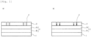
- FIG. 1 Schematic drawings showing a laminate before and after a sealing treatment ((a) before the sealing treatment, (b) after the sealing treatment)
- a laminate of an embodiment of the present invention comprises a metallic base material, a nickel-containing plating film layer formed on the metallic base material, and a gold plating film layer formed on the nickel-containing plating film layer, in which pinholes in the gold plating film layer are sealed with a fluorinated passive film having a thickness of 8 nm or greater.
- a method for producing the laminate of the embodiment of the present invention comprises a step (A) of forming a nickel-containing plating film layer on a metallic base material, a step (B) of forming a gold plating film layer on the nickel-containing plating film layer, and a sealing treatment step (C) of forming a fluorinated passive film having a thickness of 8 nm or greater in pinholes in the gold plating film layer.
- Metallic base materials used in the embodiment of the present invention have at least a surface made up of a metal.
- the metallic base materials are not particularly limited, and examples thereof are metals generally used in constituent members of semiconductor production devices, preferably including stainless steel, iron, aluminum, aluminum alloys, copper, and copper alloys.
- the metallic base materials may be subjected to pretreatment for the step (A) such as degreasing, acid cleaning, or a nickel strike treatment depending on the base materials.
- the nickel strike treatment is a preliminary plating treatment using a nickel-containing plating bath, in which the current density is preferably 5 to 20 A/dm 2 , and more preferably 5 to 10 A/dm 2 .
- the nickel strike treatment time is preferably 5 seconds or longer and 5 minutes or shorter.
- a nickel-containing plating film layer is formed on the metallic base material by the step (A).
- a nickel strike layer is formed between the metallic base material and the nickel plating film layer.
- the nickel-containing plating film layer preferably contains phosphorus, and preferably comprises a nickel-phosphorus alloy plating layer (1) having a phosphorus concentration of 8% by mass or higher and lower than 10% by mass, and a nickel-phosphorus alloy plating layer (2) having a phosphorus concentration of 10% by mass or higher and 12% by mass or lower in this order from the metallic base material.
- the nickel-containing plating film layer has a nickel content of preferably 80% by mass or higher, more preferably 85% to 95% by mass, and particularly preferably 88% to 92% by mass in relation to 100% by mass of the entirety of the nickel-containing plating film layer. Due to a nickel content within the above range, the proportion of phosphorus in the film layer increases, which exhibits excellent corrosion resistance. In addition, when electroless nickel-phosphorus alloy plating films having different phosphorus concentrations are laminated, film formation proceeds while forming pinhole defects in different positions. For this reason, disturbance hardly reaches the base material directly, and increased corrosion resistance is anticipated.
- the nickel-containing plating film layer may be formed on a metallic base material using an electroless plating bath comprising a nickel salt and a phosphorus compound as a reducer.
- nickel salts are nickel sulfate, nickel chloride, nickel acetate, and nickel carbonate.
- phosphorus compounds are sodium hypophosphite and potassium hypophosphite.
- the step (A) preferably comprises a step (a1) of forming the nickel-phosphorus alloy plating layer (1), and a step (a2) of forming the nickel-phosphorus alloy plating layer (2) after the step (a1).
- the film formation rate of the nickel-phosphorus alloy plating layer (1) is preferably 20 to 30 ⁇ m/h (hour), more preferably 22 to 25 ⁇ m/h (hour), and the film formation rate of the nickel-phosphorus alloy plating layer (2) is preferably 10 to 15 ⁇ m/h (hour), more preferably 11 to 13 ⁇ m/h (hour).
- the thus-formed nickel-phosphorus alloy plating layers (1) and (2) allow increased corrosion resistance.
- the nickel-phosphorus alloy plating film layers (1) and (2) each have a film thickness of preferably 5 ⁇ m or greater, and more preferably 7 to 25 ⁇ m. From the viewpoints of film properties of resisting pinhole formation and cost efficiency, the thickness is still more preferably from 10 to 20 ⁇ m.
- the gold plating film layer is formed on the nickel-containing plating film layer by the step (B).
- the gold content in the gold plating film is, relative to 100% by mass of the entirety of the gold plating film layer, preferably 90% by mass or greater, more preferably 99% by mass or greater, and particularly preferably 99.9% by mass or greater. Due to the gold content within the above range, corrosion resistance of the laminate of the embodiment of the present invention is stabilized.
- the gold content is obtained by a method for quantifying impurities, namely by dissolving gold plating in aqua regia to measure the gold content by atomic absorption spectrometry and inductively coupled plasma (ICP) atomic emission spectrometry.
- the thickness of the gold plating film is preferably from 0.1 ⁇ m to 1 ⁇ m, more preferably 0.2 to 0.9 ⁇ m, and particularly preferably 0.3 to 0.8 ⁇ m. It is publicly known based on conventional art that the thicker the precious metal plating film is, the more the number of pinholes is reduced, and high corrosion resistance is expected to be achievable by increasing the thickness of a precious metal plating film. Considering the high price thereof, however, it is preferred to select an appropriate thickness.
- the step (B) preferably comprises a step (b1) of forming a displacement gold plating film layer, and a step (b2) of forming a reduction gold plating film layer after the step (b1).
- nickel is dissolved from a nickel film releasing electrons, which reduce gold ions in the solution, and the reduced gold ions in the solution are deposited as a gold plating film.
- reduction gold plating gold ions in the solution are reduced by electrons released due to an oxidation reaction by a reducer, and thereby a gold plating film is deposited.
- Examples of electroless gold plating solutions are plating baths containing components such as gold potassium cyanide, gold chloride, gold sulfite, and gold thiosulfate.
- Examples of reducers are sodium hydroxide, dimethylamine borane, hexamethylenetetramine, and chain polyamines comprising an alkyl group having 3 or more carbon atoms and multiple amino groups.
- the gold plating film layer may be formed by performing displacement gold plating preferably at a temperature of 50 to 90°C for 3 to 7 minutes, more preferably at a temperature of 65 to 75°C for 3 to 7 minutes, and by performing reduction gold plating preferably at a temperature of 55 to 65°C for 7 to 15 minutes, more preferably at a temperature of 58 to 62°C for 7 to 15 minutes.
- Pinholes in the gold plating film layer are sealed with a fluorinated passive film by subjecting a surface of the gold plating film layer to a fluorination treatment in the step (C).
- the fluorinated passive film is formed only on an exposed surface of the nickel-phosphorus alloy plating layer (2b) in Fig. 1(b) .
- the fluorinated passive film is formed while growing only in a vertical direction of the fluorinated passive film 5, without being formed on a side surface inside a pinhole in the gold plating film layer 3 and without being formed on the outermost surface of the gold plating film layer 3.
- the fluorinated passive film also does not exceed the upper end of the gold plating film layer 3.
- the thickness of the fluorinated passive film is ordinarily 8 nm or greater, preferably 10 to 20 nm, and more preferably 12 to 18 nm. Due to the thickness of the fluorinated passive film within the above range, the properties of the fluorinated passive film such as durability become practically suitable.
- the thickness of the fluorinated passive film herein means the length of an obtained laminate in a lamination direction, which is, for example, equivalent to the vertical length of the fluorinated passive film 5 in Fig. 1(b) .
- a surface of the nickel-containing plating film layer exposed from pinholes in the gold plating film layer that has undergone the steps (A) and (B) is forcibly fluorinated using fluorinated gas to form a fluorinated passive film. Thereby pinholes are subjected to sealing treatment.
- the step (C) is performed in an atmosphere having a fluorinated gas concentration preferably of 8% by volume or higher, and more preferably of 10 to 25% by volume.
- the fluorination temperature is preferably 100 to 150°C, more preferably 105 to 145°C, and furthermore preferably 110 to 140°C.
- Fluorinated gas is a gas used for a fluorination treatment, and is a generic name of at least one type of a gas selected from the group consisting of fluorine (F 2 ), chlorine trifluoride (ClF 3 ), and nitrogen fluoride (NF 3 ), or a gas obtained by diluting the above gas with an inert gas.
- chlorine trifluoride when chlorine trifluoride is used, the chlorine trifluoride is pyrolyzed at a temperature of 60 to 100°C to form fluorine radicals, which are usable in a fluorination reaction.
- nitrogen trifluoride when nitrogen trifluoride is used, the nitrogen trifluoride is decomposed by plasma energy to form fluorine radicals, which are usable in a fluorination reaction.
- dilution gases accompanying the fluorinated gas are inert gases such as nitrogen gas and argon gas, and nitrogen gas is preferred.
- the concentration may be appropriately determined in accordance with reaction conditions.
- usage is preferably with a concentration of approximately 10% when factors such as cost are taken into account.
- the metallic base material is stainless steel
- fluorination is performed at a temperature of preferably 150 to 190°C, more preferably 155 to 175°C
- the metallic base material is an aluminum alloy
- fluorination is performed at a temperature of preferably 140 to 160°C, more preferably 145 to 155°C.
- the film formation temperature within the above range allows well-balanced thermal diffusion between electroless nickel-alloy plating and gold plating.
- Fluorination treatment time varies in accordance with the thickness of a fluorinated passive film to be formed, and the amount of time required for exhibiting excellent corrosion resistance is preferably 20 to 100 hours, and more preferably 30 to 80 hours.
- a surface of stainless steel (SUS316L) that was worked into a test piece having a size of 15 mm (length) x 15 mm (width) x 1 mm (thickness) was subjected to a pretreatment comprising degreasing, acid cleaning, and a nickel strike treatment.
- the acid cleaning was performed using hydrochloric acid as a cleaning agent at room temperature for 25 seconds.
- an electroless nickel-phosphorus alloy plating film layer (1) having a phosphorus content of 8% by mass or greater and less than 10% by mass in the formed film was formed using an electroless nickel-phosphorus plating chemical "NIMUDEN (trade name) NSX" (produced by C.
- an electroless nickel-phosphorus alloy plating film layer (2) having a phosphorus content of 10% by mass or greater to 12% by mass or less in the formed film was formed using an electroless nickel-phosphorus plating chemical "NIMUDEN (trade name) HDX" (produced by C. Uyemura & Co., Ltd.) at a film formation rate of 10 ⁇ m / 50 minutes.
- NIMUDEN electroless nickel-phosphorus plating chemical
- the stainless steel having the nickel-containing plating film layer and the gold plating film layer formed in the steps (A) and (B) was placed inside an atmospheric pressure gas-phase flow reactor, and the temperature inside the reactor was increased to 115°C. Thereafter, the atmosphere was replaced with nitrogen gas, followed by the introduction of 10% by volume of fluorine gas diluted with nitrogen gas to replace the nitrogen gas in the reactor with 10% by volume of fluorine gas. After complete replacement, the state was maintained for 36 hours, and exposed parts of the substrate electroless nickel-phosphorus film, which were exposed due to pinholes formed during the gold plating, were forcibly fluorinated to form a fluorinated passive film.
- the obtained fluorinated passive film was analyzed with W-SEM "JSM-IT200" (produced by JEOL Ltd). It was confirmed that the film thickness of the fluorinated passive film was 10 nm.
- the film thickness of the fluorinated passive film herein means the length of an obtained laminate in a lamination direction, which is, for example, equivalent to the vertical length of the fluorinated passive film 5 in Fig. 1(b) .
- a fluorinated passive film was formed in the same manner as described in Example 1 except for changing the time of the forcible fluorination using 10% by volume of fluorine gas diluted with nitrogen gas in the step (C) described in Example 1 to 72 hours.
- the thickness of the obtained fluorinated passive film was determined in the same manner as described in Example 1. It was confirmed that the film thickness was 13 nm.
- Example 1 An aluminum alloy (A5052) was used instead of the stainless steel (SUS316L) in Example 1, a pretreatment comprising degreasing, activation treatment, acid cleaning, and a zinc replacement treatment was performed, and thereafter the steps (A) and (B) were performed in the same manner as described in Example 1.
- the activation treatment was performed using an acid mixture of ammonium acid fluoride and nitric acid as a treating agent at room temperature for 30 seconds.
- the acid cleaning was performed using nitric acid as a cleaning agent at room temperature for 25 seconds.
- the zinc replacement treatment was performed using a zincate bath as a treating agent at room temperature for 25 seconds. The acid cleaning and the zinc replacement treatment were each performed twice under the above conditions.
- a fluorinated passive film was formed on the gold plating film in the same manner as described in Example 2 except for adjusting the forcible fluorination temperature to 105°C.
- the thickness of the obtained fluorinated passive film was determined in the same manner as described in Example 1. It was confirmed that the film thickness was 10 nm.
- the stainless steel having nickel-containing plating film layers and a gold plating film layer was exposed to the atmosphere to form a natural oxide film.
- the thickness of the obtained natural oxide film was determined in the same manner as described in Example 1. It was confirmed that the film thickness was 7 nm.
- the step (A) described in Example 1 was performed and thereafter the following treatment was performed.
- the stainless steel having a nickel-containing plating film layer was placed inside the atmospheric pressure gas-phase flow reactor, and the temperature inside the reactor was increased to 300°C. Thereafter, the atmosphere was replaced with nitrogen gas, followed by the introduction of 100% by volume of oxygen gas to replace nitrogen gas with oxygen gas. After complete replacement, the state was maintained for 12 hours. Subsequently, 10% by volume of fluorine gas diluted with nitrogen gas was introduced and this state was maintained for 12 hours to form a nickel fluoride (NiF 2 ) film on the nickel-containing plating film layer. Thereafter, nitrogen gas was injected for 12 hours to stabilize the formed film.
- NiF 2 nickel fluoride
- a test piece in a size of 15 mm (length) x 15 mm (width) x 1 mm (thickness) was immersed in a 35% by mass hydrochloric acid solution at a temperature of 25°C for 5 hours. Based on the reduced amount of mass [mg/dm 2 ] before and after the immersion, hydrochloric acid corrosion resistance was evaluated in accordance with the following criteria.
- SUS stainless steel
- Al aluminum alloy
Landscapes
- Chemical & Material Sciences (AREA)
- Organic Chemistry (AREA)
- Metallurgy (AREA)
- Chemical Kinetics & Catalysis (AREA)
- Engineering & Computer Science (AREA)
- Materials Engineering (AREA)
- Mechanical Engineering (AREA)
- General Chemical & Material Sciences (AREA)
- Electrochemistry (AREA)
- Inorganic Chemistry (AREA)
- Chemically Coating (AREA)
- Electroplating Methods And Accessories (AREA)
- Laminated Bodies (AREA)
- Other Surface Treatments For Metallic Materials (AREA)
Abstract
Description
- The present invention relates to a laminate and a method for producing the same. More specifically, the present invention relates to a laminate suitable as a constituent member of devices such as semiconductor production devices, and a method for producing the laminate.
- In a semiconductor production process, special halogen gases which are strongly reactive and corrosive such as fluorine, hydrogen chloride, boron trichloride, nitrogen trifluoride, chlorine trifluoride, and hydrogen bromide (these may be hereinafter referred to as "corrosive gas"), have conventionally been used in a dry etching step and in the cleaning of production devices for example.
- However, when the above corrosive gas reacts with the moisture contained in an atmosphere and is hydrolyzed, products such as hydrogen fluoride, oxalic acid, and hydrogen chloride are generated. The products are problematic since they easily corrode metallic surfaces of constituent members such as valves, couplings, piping, and reaction chambers during the use of the corrosive gas.
- Meanwhile, pinholes on a plating surface may also be a reason why corrosion proceeds. There seem to be several factors in causing pinholes, for example, such that hydrogen gas generated by a plating reaction forms bubbles during the formation of a plating film to inhibit film formation, or such that impurities (such as an oxide film, contamination, and oil) remaining on a base material are not eliminated in a pretreatment step, resulting in the inhibition of film formation.
- In order to increase corrosion resistance, methods in which a metallic base material is plated with a nickel-phosphorus alloy to form a fluorinated passive film of nickel have been hitherto performed (see for
example Patent Literature 1 to Patent Literature 3). However, the methods are sometimes insufficient. - There is also a method in which a metallic base material is plated with a nickel-tungsten alloy and a thick fluorinated passive film of nickel is formed at a low temperature by utilizing the standard enthalpy of formation of WF6 formed by a fluorination reaction. However, the method, which is electroplating, has a restriction such that members to which the method is applicable are limited (see Patent Literature 4).
-
- Patent Literature 1:
JP 2954716 B2 - Patent Literature 2:
JP 3094000 B2 - Patent Literature 3:
JP 2004-360066 A - Patent Literature 4:
JP 2008-056978 A - What is intended by the present invention is to resolve the above problems associated with conventional art. The objects of the present invention are to provide a metallic material which can be employed as a constituent member of a semiconductor production device and also excels in corrosion resistance, and to provide a method for producing the metallic material.
- The present invention relates to the following [1] to [12] for example.
- [1] A laminate comprising a metallic base material, a nickel-containing plating film layer formed on the metallic base material, and a gold plating film layer formed on the nickel-containing plating film layer, in which pinholes in the gold plating film layer are sealed with a fluorinated passive film having a thickness of 8 nm or greater.
- [2] The laminate described in [1], in which the metallic base material comprises at least one metal selected from the group consisting of stainless steel, iron, aluminum, aluminum alloys, copper, and copper alloys.
- [3] The laminate described in [1] or [2], having a nickel strike layer between the metallic base material and the nickel-containing plating film layer.
- [4] The laminate described in any one of [1] to [3], in which the nickel-containing plating film layer comprises a nickel-phosphorus alloy plating layer (1) having a phosphorus concentration of 8% by mass or higher and lower than 10% by mass, and a nickel-phosphorus alloy plating layer (2) having a phosphorus concentration of 10% by mass or higher and 12% by mass or lower in this order from the metallic base material.
- [5] The laminate described in any one of [1] to [4], in which the gold plating film layer comprises a displacement gold plating film layer and a reduction gold plating film layer in this order from the nickel-containing plating film layer.
- [6] A constituent member of a semiconductor production device, which is made up of the laminate described in any one of [1] to [5].
- [7] A method for producing a laminate, comprising a step (A) of forming a nickel-containing plating film layer on a metallic base material, a step (B) of forming a gold plating film layer on the nickel-containing plating film layer, and a sealing treatment step (C) of forming a fluorinated passive film having a thickness of 8 nm or greater in pinholes in the gold plating film layer.
- [8] The method for producing a laminate described in [7], in which the sealing treatment step (C) is performed in an atmosphere having a fluorinated gas concentration of 8% by volume or higher and a temperature of 100 to 150°C.
- [9] The method for producing a laminate described in [7] or [8], in which the metallic base material comprises at least one metal selected from the group consisting of stainless steel, iron, aluminum, aluminum alloys, copper, and copper alloys.
- [10] The method for producing a laminate described in any one of [7] to [9], comprising a step of subjecting the metallic base material to a nickel strike treatment under the condition of a current density being 5 to 20 A/dm2 before the step (A).
- [11] The method for producing a laminate described in any one of [7] to [10], in which the step (A) comprises a step (a1) of forming a nickel-phosphorus alloy plating layer (1) having a phosphorus concentration of 8% by mass or higher and lower than 10% by mass, and after the step (a1), a step (a2) of forming a nickel-phosphorus alloy plating layer (2) having a phosphorus concentration of 10% by mass or higher and 12% by mass or lower.
- [12] The method for producing a laminate described in any one of [7] to [11], in which the step (B) comprises a step (b1) of forming a displacement gold plating film layer, and after the step (b1), a step (b2) of forming a reduction gold plating film layer.
- The present invention is capable of providing laminates having excellent corrosion resistance, particularly excellent corrosion resistance to acids.
- [
Fig. 1 ] Schematic drawings showing a laminate before and after a sealing treatment ((a) before the sealing treatment, (b) after the sealing treatment) - An embodiment of the present invention is specifically described below.
- A laminate of an embodiment of the present invention comprises a metallic base material, a nickel-containing plating film layer formed on the metallic base material, and a gold plating film layer formed on the nickel-containing plating film layer, in which pinholes in the gold plating film layer are sealed with a fluorinated passive film having a thickness of 8 nm or greater.
- A method for producing the laminate of the embodiment of the present invention comprises a step (A) of forming a nickel-containing plating film layer on a metallic base material, a step (B) of forming a gold plating film layer on the nickel-containing plating film layer, and a sealing treatment step (C) of forming a fluorinated passive film having a thickness of 8 nm or greater in pinholes in the gold plating film layer.
- Metallic base materials used in the embodiment of the present invention have at least a surface made up of a metal. The metallic base materials are not particularly limited, and examples thereof are metals generally used in constituent members of semiconductor production devices, preferably including stainless steel, iron, aluminum, aluminum alloys, copper, and copper alloys.
- In order to increase the adhesion to a nickel-containing plating film layer, the metallic base materials may be subjected to pretreatment for the step (A) such as degreasing, acid cleaning, or a nickel strike treatment depending on the base materials. The nickel strike treatment is a preliminary plating treatment using a nickel-containing plating bath, in which the current density is preferably 5 to 20 A/dm2, and more preferably 5 to 10 A/dm2. In addition, the nickel strike treatment time is preferably 5 seconds or longer and 5 minutes or shorter.
- A nickel-containing plating film layer is formed on the metallic base material by the step (A). When the metallic base material is subjected to a nickel strike treatment, a nickel strike layer is formed between the metallic base material and the nickel plating film layer.
- From the viewpoint of increased corrosion resistance, the nickel-containing plating film layer preferably contains phosphorus, and preferably comprises a nickel-phosphorus alloy plating layer (1) having a phosphorus concentration of 8% by mass or higher and lower than 10% by mass, and a nickel-phosphorus alloy plating layer (2) having a phosphorus concentration of 10% by mass or higher and 12% by mass or lower in this order from the metallic base material.
- The nickel-containing plating film layer has a nickel content of preferably 80% by mass or higher, more preferably 85% to 95% by mass, and particularly preferably 88% to 92% by mass in relation to 100% by mass of the entirety of the nickel-containing plating film layer. Due to a nickel content within the above range, the proportion of phosphorus in the film layer increases, which exhibits excellent corrosion resistance. In addition, when electroless nickel-phosphorus alloy plating films having different phosphorus concentrations are laminated, film formation proceeds while forming pinhole defects in different positions. For this reason, disturbance hardly reaches the base material directly, and increased corrosion resistance is anticipated.
- The nickel-containing plating film layer may be formed on a metallic base material using an electroless plating bath comprising a nickel salt and a phosphorus compound as a reducer. Examples of nickel salts are nickel sulfate, nickel chloride, nickel acetate, and nickel carbonate. Examples of phosphorus compounds are sodium hypophosphite and potassium hypophosphite.
- The step (A) preferably comprises a step (a1) of forming the nickel-phosphorus alloy plating layer (1), and a step (a2) of forming the nickel-phosphorus alloy plating layer (2) after the step (a1).
- The film formation rate of the nickel-phosphorus alloy plating layer (1) is preferably 20 to 30 µm/h (hour), more preferably 22 to 25 µm/h (hour), and the film formation rate of the nickel-phosphorus alloy plating layer (2) is preferably 10 to 15 µm/h (hour), more preferably 11 to 13 µm/h (hour). The thus-formed nickel-phosphorus alloy plating layers (1) and (2) allow increased corrosion resistance. The nickel-phosphorus alloy plating film layers (1) and (2) each have a film thickness of preferably 5 µm or greater, and more preferably 7 to 25 µm. From the viewpoints of film properties of resisting pinhole formation and cost efficiency, the thickness is still more preferably from 10 to 20 µm.
- The gold plating film layer is formed on the nickel-containing plating film layer by the step (B).
- The gold content in the gold plating film is, relative to 100% by mass of the entirety of the gold plating film layer, preferably 90% by mass or greater, more preferably 99% by mass or greater, and particularly preferably 99.9% by mass or greater. Due to the gold content within the above range, corrosion resistance of the laminate of the embodiment of the present invention is stabilized. The gold content is obtained by a method for quantifying impurities, namely by dissolving gold plating in aqua regia to measure the gold content by atomic absorption spectrometry and inductively coupled plasma (ICP) atomic emission spectrometry.
- From the viewpoints of film properties of resisting pinhole formation and cost efficiency, the thickness of the gold plating film is preferably from 0.1 µm to 1 µm, more preferably 0.2 to 0.9 µm, and particularly preferably 0.3 to 0.8 µm. It is publicly known based on conventional art that the thicker the precious metal plating film is, the more the number of pinholes is reduced, and high corrosion resistance is expected to be achievable by increasing the thickness of a precious metal plating film. Considering the high price thereof, however, it is preferred to select an appropriate thickness.
- Methods for forming the gold plating film layer are not particularly limited and an electroless gold plating method is preferred. In an electroless gold plating method, it is preferred to perform displacement gold plating and thereafter reduction gold plating. Namely, the step (B) preferably comprises a step (b1) of forming a displacement gold plating film layer, and a step (b2) of forming a reduction gold plating film layer after the step (b1).
- In displacement gold plating, nickel is dissolved from a nickel film releasing electrons, which reduce gold ions in the solution, and the reduced gold ions in the solution are deposited as a gold plating film. In reduction gold plating, gold ions in the solution are reduced by electrons released due to an oxidation reaction by a reducer, and thereby a gold plating film is deposited.
- Examples of electroless gold plating solutions are plating baths containing components such as gold potassium cyanide, gold chloride, gold sulfite, and gold thiosulfate. Examples of reducers are sodium hydroxide, dimethylamine borane, hexamethylenetetramine, and chain polyamines comprising an alkyl group having 3 or more carbon atoms and multiple amino groups.
- The gold plating film layer may be formed by performing displacement gold plating preferably at a temperature of 50 to 90°C for 3 to 7 minutes, more preferably at a temperature of 65 to 75°C for 3 to 7 minutes, and by performing reduction gold plating preferably at a temperature of 55 to 65°C for 7 to 15 minutes, more preferably at a temperature of 58 to 62°C for 7 to 15 minutes.
- Pinholes in the gold plating film layer are sealed with a fluorinated passive film by subjecting a surface of the gold plating film layer to a fluorination treatment in the step (C).
- The fluorinated passive film is formed only on an exposed surface of the nickel-phosphorus alloy plating layer (2b) in
Fig. 1(b) . In other words, the fluorinated passive film is formed while growing only in a vertical direction of the fluorinatedpassive film 5, without being formed on a side surface inside a pinhole in the goldplating film layer 3 and without being formed on the outermost surface of the goldplating film layer 3. The fluorinated passive film also does not exceed the upper end of the goldplating film layer 3. - The thickness of the fluorinated passive film is ordinarily 8 nm or greater, preferably 10 to 20 nm, and more preferably 12 to 18 nm. Due to the thickness of the fluorinated passive film within the above range, the properties of the fluorinated passive film such as durability become practically suitable. The thickness of the fluorinated passive film herein means the length of an obtained laminate in a lamination direction, which is, for example, equivalent to the vertical length of the fluorinated
passive film 5 inFig. 1(b) . - In the step (C), a surface of the nickel-containing plating film layer exposed from pinholes in the gold plating film layer that has undergone the steps (A) and (B) is forcibly fluorinated using fluorinated gas to form a fluorinated passive film. Thereby pinholes are subjected to sealing treatment.
- The step (C) is performed in an atmosphere having a fluorinated gas concentration preferably of 8% by volume or higher, and more preferably of 10 to 25% by volume. The fluorination temperature is preferably 100 to 150°C, more preferably 105 to 145°C, and furthermore preferably 110 to 140°C.
- Fluorinated gas is a gas used for a fluorination treatment, and is a generic name of at least one type of a gas selected from the group consisting of fluorine (F2), chlorine trifluoride (ClF3), and nitrogen fluoride (NF3), or a gas obtained by diluting the above gas with an inert gas.
- For example, when chlorine trifluoride is used, the chlorine trifluoride is pyrolyzed at a temperature of 60 to 100°C to form fluorine radicals, which are usable in a fluorination reaction. In addition, when nitrogen trifluoride is used, the nitrogen trifluoride is decomposed by plasma energy to form fluorine radicals, which are usable in a fluorination reaction.
- Examples of dilution gases accompanying the fluorinated gas are inert gases such as nitrogen gas and argon gas, and nitrogen gas is preferred.
- When the fluorinated gas is diluted for use, the concentration may be appropriately determined in accordance with reaction conditions. In the case of fluorine, for example, usage is preferably with a concentration of approximately 10% when factors such as cost are taken into account.
- When the metallic base material is stainless steel, fluorination is performed at a temperature of preferably 150 to 190°C, more preferably 155 to 175°C, and when the metallic base material is an aluminum alloy, fluorination is performed at a temperature of preferably 140 to 160°C, more preferably 145 to 155°C. The film formation temperature within the above range allows well-balanced thermal diffusion between electroless nickel-alloy plating and gold plating.
- Fluorination treatment time varies in accordance with the thickness of a fluorinated passive film to be formed, and the amount of time required for exhibiting excellent corrosion resistance is preferably 20 to 100 hours, and more preferably 30 to 80 hours.
- The present invention is more specifically described below with reference to, but not limited to, examples.
- A surface of stainless steel (SUS316L) that was worked into a test piece having a size of 15 mm (length) x 15 mm (width) x 1 mm (thickness) was subjected to a pretreatment comprising degreasing, acid cleaning, and a nickel strike treatment. The acid cleaning was performed using hydrochloric acid as a cleaning agent at room temperature for 25 seconds. On a surface of the stainless steel that underwent the nickel strike treatment, an electroless nickel-phosphorus alloy plating film layer (1) having a phosphorus content of 8% by mass or greater and less than 10% by mass in the formed film was formed using an electroless nickel-phosphorus plating chemical "NIMUDEN (trade name) NSX" (produced by C. Uyemura & Co., Ltd.) under the conditions of the plating temperature being 90°C and the pH value being 4.5 to 4.8, at a film formation rate of 10 µm / 25 minutes. Subsequently, an electroless nickel-phosphorus alloy plating film layer (2) having a phosphorus content of 10% by mass or greater to 12% by mass or less in the formed film was formed using an electroless nickel-phosphorus plating chemical "NIMUDEN (trade name) HDX" (produced by C. Uyemura & Co., Ltd.) at a film formation rate of 10 µm / 50 minutes. Thereby a nickel-containing plating film layer having a total thickness of 20 µm was formed on the stainless steel that underwent the nickel strike treatment.
- Two types of electroless gold plating solutions "Flash Gold NC (displacement type)" and "Self Gold OTK-IT (reduction type)" (both produced by Okuno Pharmaceutical Co., Ltd.,) were used in this order. On the nickel-containing plating film layers formed in the step (A), a treatment at a displacement plating temperature of 70°C for 5 minutes and a treatment at a reduction plating temperature of 60°C for 10 minutes were each performed in this order to form gold plating film layers having a total thickness of 0.6 µm.
- The stainless steel having the nickel-containing plating film layer and the gold plating film layer formed in the steps (A) and (B) was placed inside an atmospheric pressure gas-phase flow reactor, and the temperature inside the reactor was increased to 115°C. Thereafter, the atmosphere was replaced with nitrogen gas, followed by the introduction of 10% by volume of fluorine gas diluted with nitrogen gas to replace the nitrogen gas in the reactor with 10% by volume of fluorine gas. After complete replacement, the state was maintained for 36 hours, and exposed parts of the substrate electroless nickel-phosphorus film, which were exposed due to pinholes formed during the gold plating, were forcibly fluorinated to form a fluorinated passive film. The obtained fluorinated passive film was analyzed with W-SEM "JSM-IT200" (produced by JEOL Ltd). It was confirmed that the film thickness of the fluorinated passive film was 10 nm. The film thickness of the fluorinated passive film herein means the length of an obtained laminate in a lamination direction, which is, for example, equivalent to the vertical length of the fluorinated
passive film 5 inFig. 1(b) . - A fluorinated passive film was formed in the same manner as described in Example 1 except for changing the time of the forcible fluorination using 10% by volume of fluorine gas diluted with nitrogen gas in the step (C) described in Example 1 to 72 hours. The thickness of the obtained fluorinated passive film was determined in the same manner as described in Example 1. It was confirmed that the film thickness was 13 nm.
- An aluminum alloy (A5052) was used instead of the stainless steel (SUS316L) in Example 1, a pretreatment comprising degreasing, activation treatment, acid cleaning, and a zinc replacement treatment was performed, and thereafter the steps (A) and (B) were performed in the same manner as described in Example 1.
- The activation treatment was performed using an acid mixture of ammonium acid fluoride and nitric acid as a treating agent at room temperature for 30 seconds. The acid cleaning was performed using nitric acid as a cleaning agent at room temperature for 25 seconds. The zinc replacement treatment was performed using a zincate bath as a treating agent at room temperature for 25 seconds. The acid cleaning and the zinc replacement treatment were each performed twice under the above conditions.
- In the step (C), a fluorinated passive film was formed on the gold plating film in the same manner as described in Example 2 except for adjusting the forcible fluorination temperature to 105°C. The thickness of the obtained fluorinated passive film was determined in the same manner as described in Example 1. It was confirmed that the film thickness was 10 nm.
- By performing only the step (A) described in Example 1, a nickel-containing plating film layer having a total thickness of 20 µm was formed on a surface of stainless steel.
- After performing the steps (A) and (B) described in Example 1, the stainless steel having nickel-containing plating film layers and a gold plating film layer, was exposed to the atmosphere to form a natural oxide film. The thickness of the obtained natural oxide film was determined in the same manner as described in Example 1. It was confirmed that the film thickness was 7 nm.
- The step (A) described in Example 1 was performed and thereafter the following treatment was performed. The stainless steel having a nickel-containing plating film layer was placed inside the atmospheric pressure gas-phase flow reactor, and the temperature inside the reactor was increased to 300°C. Thereafter, the atmosphere was replaced with nitrogen gas, followed by the introduction of 100% by volume of oxygen gas to replace nitrogen gas with oxygen gas. After complete replacement, the state was maintained for 12 hours. Subsequently, 10% by volume of fluorine gas diluted with nitrogen gas was introduced and this state was maintained for 12 hours to form a nickel fluoride (NiF2) film on the nickel-containing plating film layer. Thereafter, nitrogen gas was injected for 12 hours to stabilize the formed film.
- The films on the surfaces of the metallic base materials obtained in the above Examples 1 to 3 and the Comparative Examples 1 to 3 were evaluated by the method below. The evaluation results are summarized in Table 1.
- A test piece in a size of 15 mm (length) x 15 mm (width) x 1 mm (thickness) was immersed in a 35% by mass hydrochloric acid solution at a temperature of 25°C for 5 hours. Based on the reduced amount of mass [mg/dm2] before and after the immersion, hydrochloric acid corrosion resistance was evaluated in accordance with the following criteria.
-
- A: less than 0.1 mg/dm2
- B: 0.1 mg/dm2 or greater and less than 3 mg/dm2
- C: 3 mg/dm2 or greater
-
Table 1 Example 1 Example 2 Example 3 Comparative Example 1 Comparative Example 2 Comparative Example 3 Metallic base material SUS SUS Al SUS SUS SUS Nickel-containing plating film layer Formed Formed Formed Formed Formed Formed Gold plating film layer Formed Formed Formed Not formed Formed Not formed Sealing treatment Performed Performed Performed Not performed Performed Not performed Thickness of fluorinated passive film [nm] 10 13 10 - - - Thickness of natural oxide film [nm] - - - - 7 - NiF2 treatment Not performed Not performed Not performed Not performed Not performed Performed Hydrochloric acid corrosion resistance B A B C C C - In the table, SUS means stainless steel (SUS316L) and Al means an aluminum alloy (A5052).
-
- 1
- Metallic base material
- 2
- Nickel-containing plating film layer
- 2a
- Nickel-phosphorus alloy plating layer (1)
- 2b
- Nickel-phosphorus alloy plating layer (2)
- 3
- Gold plating film layer
- 4
- Pinhole
- 5
- Fluorinated passive film
Claims (12)
- A laminate comprising a metallic base material, a nickel-containing plating film layer formed on the metallic base material, and a gold plating film layer formed on the nickel-containing plating film layer,
wherein pinholes in the gold plating film layer are sealed with a fluorinated passive film having a thickness of 8 nm or greater. - The laminate according to claim 1, wherein the metallic base material comprises at least a metal selected from the group consisting of stainless steel, iron, aluminum, aluminum alloys, copper, and copper alloys.
- The laminate according to claim 1 or 2, having a nickel strike layer between the metallic base material and the nickel-containing plating film layer.
- The laminate according to any one of claims 1 to 3, wherein the nickel-containing plating film layer comprises a nickel-phosphorus alloy plating layer (1) having a phosphorus concentration of 8% by mass or higher and lower than 10% by mass, and a nickel-phosphorus alloy plating layer (2) having a phosphorus concentration of 10% by mass or higher and 12% by mass or lower in this order from the metallic base material.
- The laminate according to any one of claims 1 to 4, wherein the gold plating film layer comprises a displacement gold plating film layer and a reduction gold plating film layer in this order from the nickel-containing plating film layer.
- A constituent member of a semiconductor production device, made up of the laminate according to any one of claims 1 to 5.
- A method for producing a laminate, comprisinga step (A) of forming a nickel-containing plating film layer on a metallic base material,a step (B) of forming a gold plating film layer on the nickel-containing plating film layer, anda sealing treatment step (C) of forming a fluorinated passive film having a thickness of 8 nm or greater in pinholes in the gold plating film layer.
- The method for producing a laminate according to claim 7, wherein the sealing treatment step (C) is performed in an atmosphere in which a fluorinated gas concentration is 8% by volume or higher and a temperature is 100 to 150°C.
- The method for producing a laminate according to claim 7 or 8, wherein the metallic base material comprises at least one metal selected from the group consisting of stainless steel, iron, aluminum, aluminum alloys, copper, and copper alloys.
- The method for producing a laminate according to any one of claims 7 to 9, comprising a step of subjecting the metallic base material to a nickel strike treatment under the condition of a current density of 5 to 20 A/dm2 before the step (A).
- The method for producing a laminate according to any one of claims 7 to 10, wherein the step (A) comprises a step (a1) of forming a nickel-phosphorus alloy plating layer (1) having a phosphorus concentration of 8% by mass or higher and lower than 10% by mass, and a step (a2) of forming a nickel-phosphorus alloy plating layer (2) having a phosphorus concentration of 10% by mass or higher and 12% by mass or lower after the step (a1).
- The method for producing a laminate according to any one of claims 7 to 11, wherein the step (B) comprises a step (b1) of forming a displacement gold plating film layer, and a step (b2) of forming a reduction gold plating film layer after the step (b1).
Applications Claiming Priority (2)
| Application Number | Priority Date | Filing Date | Title |
|---|---|---|---|
| JP2019186772 | 2019-10-10 | ||
| PCT/JP2020/034516 WO2021070561A1 (en) | 2019-10-10 | 2020-09-11 | Multilayer body and method for producing same |
Publications (2)
| Publication Number | Publication Date |
|---|---|
| EP4043611A1 true EP4043611A1 (en) | 2022-08-17 |
| EP4043611A4 EP4043611A4 (en) | 2023-11-01 |
Family
ID=75437872
Family Applications (1)
| Application Number | Title | Priority Date | Filing Date |
|---|---|---|---|
| EP20873652.0A Pending EP4043611A4 (en) | 2019-10-10 | 2020-09-11 | MULTI-LAYER BODY AND PRODUCTION PROCESS THEREOF |
Country Status (8)
| Country | Link |
|---|---|
| US (1) | US12116671B2 (en) |
| EP (1) | EP4043611A4 (en) |
| JP (1) | JP7593324B2 (en) |
| KR (1) | KR102727364B1 (en) |
| CN (2) | CN113874549A (en) |
| SG (1) | SG11202113223VA (en) |
| TW (1) | TWI753581B (en) |
| WO (1) | WO2021070561A1 (en) |
Families Citing this family (2)
| Publication number | Priority date | Publication date | Assignee | Title |
|---|---|---|---|---|
| SG11202112883PA (en) * | 2019-07-31 | 2021-12-30 | Showa Denko Kk | Laminate and method for producing same |
| US20240247379A1 (en) * | 2023-01-20 | 2024-07-25 | Applied Materials, Inc. | Formation of metallic films on electroless metal plating of surfaces |
Family Cites Families (23)
| Publication number | Priority date | Publication date | Assignee | Title |
|---|---|---|---|---|
| JP2954716B2 (en) | 1990-03-08 | 1999-09-27 | 三菱アルミニウム株式会社 | Industrial material having a fluorinated passivation film and method for producing the same |
| JPH06132582A (en) | 1992-10-15 | 1994-05-13 | Komatsu Ltd | Excimer laser device |
| US5373523A (en) | 1992-10-15 | 1994-12-13 | Kabushiki Kaisha Komatsu Seisakusho | Excimer laser apparatus |
| JP3114428B2 (en) | 1993-04-28 | 2000-12-04 | ぺんてる株式会社 | Manufacturing method of precious metal plating |
| US6280597B1 (en) | 1997-09-12 | 2001-08-28 | Showa Denko K.K. | Fluorinated metal having a fluorinated layer and process for its production |
| JP3094000B2 (en) | 1997-09-12 | 2000-10-03 | 昭和電工株式会社 | Metal material or metal film having fluorinated surface layer and fluoridation method |
| JP4168209B2 (en) | 1997-12-02 | 2008-10-22 | 忠弘 大見 | A material in which a fluororesin is formed on the surface of a fluorinated passive film and various devices and parts using the material |
| JP2002241954A (en) | 2001-12-19 | 2002-08-28 | Purotonikusu Kenkyusho:Kk | Composite gold plating film, production method therefor and electric contact having the composite gold plating film |
| JP3094000U (en) | 2002-11-12 | 2003-05-23 | 株式会社金杉工芸 | Eyeglass lens cleaner |
| JP2004360066A (en) | 2003-05-09 | 2004-12-24 | Showa Denko Kk | Corrosion resistant material, and its production method |
| JP2005063991A (en) * | 2003-08-08 | 2005-03-10 | Sumitomo Electric Ind Ltd | Semiconductor manufacturing equipment |
| JP4362599B2 (en) | 2004-03-05 | 2009-11-11 | Dowaメタルテック株式会社 | Metal member and electrical contact using the same |
| JP5000236B2 (en) | 2006-08-30 | 2012-08-15 | 昭和電工株式会社 | Metal material whose outermost layer is a nickel fluoride film and method for producing the same |
| JP2008260646A (en) | 2007-04-10 | 2008-10-30 | Toshiba Mach Co Ltd | Molding die for molding selenium-containing glass and manufacturing method of the same |
| JP2010037603A (en) | 2008-08-05 | 2010-02-18 | Sumitomo Metal Mining Co Ltd | Connection terminal part and method for producing the same |
| JP5612355B2 (en) | 2009-07-15 | 2014-10-22 | 株式会社Kanzacc | Plating structure and method of manufacturing electrical material |
| GB2485419B (en) | 2010-11-15 | 2015-02-25 | Semblant Ltd | Method for reducing creep corrosion |
| US8574722B2 (en) * | 2011-05-09 | 2013-11-05 | Tyco Electronics Corporation | Corrosion resistant electrical conductor |
| CN103668369A (en) | 2014-01-08 | 2014-03-26 | 苏州道蒙恩电子科技有限公司 | Electric plating method capable of improving anti-corrosion performance of metal element |
| JP2016160504A (en) | 2015-03-03 | 2016-09-05 | 学校法人関東学院 | Method for forming electroless Ni / Au plating film and electroless Ni / Au plating film obtained by the method |
| US10982811B2 (en) | 2016-04-05 | 2021-04-20 | Kanto Denka Kogyo, Co., Ltd. | Material, storage container using the material, valve attached to the storage container, method of storing ClF and method of using ClF storage container |
| CN110249074B (en) | 2017-02-15 | 2021-11-02 | 三菱电机株式会社 | Semiconductor element and method of manufacturing the same |
| CN108359966A (en) | 2017-09-30 | 2018-08-03 | 深圳市正天伟科技有限公司 | A kind of half replaces semi-reduction type chemical gold plating liquid and its application process |
-
2020
- 2020-09-11 CN CN202080037980.6A patent/CN113874549A/en active Pending
- 2020-09-11 EP EP20873652.0A patent/EP4043611A4/en active Pending
- 2020-09-11 JP JP2021550540A patent/JP7593324B2/en active Active
- 2020-09-11 SG SG11202113223VA patent/SG11202113223VA/en unknown
- 2020-09-11 US US17/614,222 patent/US12116671B2/en active Active
- 2020-09-11 KR KR1020217038106A patent/KR102727364B1/en active Active
- 2020-09-11 CN CN202510750800.3A patent/CN120575159A/en active Pending
- 2020-09-11 WO PCT/JP2020/034516 patent/WO2021070561A1/en not_active Ceased
- 2020-09-22 TW TW109132667A patent/TWI753581B/en active
Also Published As
| Publication number | Publication date |
|---|---|
| US20220228266A1 (en) | 2022-07-21 |
| EP4043611A4 (en) | 2023-11-01 |
| WO2021070561A1 (en) | 2021-04-15 |
| TW202125594A (en) | 2021-07-01 |
| SG11202113223VA (en) | 2021-12-30 |
| JPWO2021070561A1 (en) | 2021-04-15 |
| CN113874549A (en) | 2021-12-31 |
| KR102727364B1 (en) | 2024-11-08 |
| CN120575159A (en) | 2025-09-02 |
| US12116671B2 (en) | 2024-10-15 |
| JP7593324B2 (en) | 2024-12-03 |
| KR20220004689A (en) | 2022-01-11 |
| TWI753581B (en) | 2022-01-21 |
Similar Documents
| Publication | Publication Date | Title |
|---|---|---|
| EP0902101B1 (en) | Metallic material or film having fluorinated surface layer, and fluorination process | |
| US12116671B2 (en) | Laminate and method for producing same | |
| US12031213B2 (en) | Laminate | |
| US20160108254A1 (en) | Zinc immersion coating solutions, double-zincate method, method of forming a metal plating film, and semiconductor device | |
| US12064937B2 (en) | Laminate and method for producing same | |
| JP2004360066A (en) | Corrosion resistant material, and its production method | |
| JP6501280B2 (en) | Chromium plating solution, electroplating method and manufacturing method of chromium plating solution | |
| EP4177376A1 (en) | Metal displacement solution and corresponding method for surface treatment of aluminum or aluminum alloy | |
| JP6620513B2 (en) | Method for producing stainless steel material, and chemical conversion treatment method for stainless steel material | |
| JP5000236B2 (en) | Metal material whose outermost layer is a nickel fluoride film and method for producing the same | |
| EP4293136A1 (en) | Etchant and method of surface treatment of aluminum or aluminum alloy | |
| EP3378974B1 (en) | Method of forming nickel film and use of nickel solution for the method | |
| JP2006089822A (en) | Member covered by halogen corrosion-resistant film, and method for manufacturing the same | |
| KR20230050875A (en) | Acidic zincate composition for aluminum or aluminum alloy and zincate treatment method using the same | |
| HK1020442A (en) | Metallic material or film having fluorinated surface layer, and fluorination process |
Legal Events
| Date | Code | Title | Description |
|---|---|---|---|
| STAA | Information on the status of an ep patent application or granted ep patent |
Free format text: STATUS: THE INTERNATIONAL PUBLICATION HAS BEEN MADE |
|
| PUAI | Public reference made under article 153(3) epc to a published international application that has entered the european phase |
Free format text: ORIGINAL CODE: 0009012 |
|
| STAA | Information on the status of an ep patent application or granted ep patent |
Free format text: STATUS: REQUEST FOR EXAMINATION WAS MADE |
|
| 17P | Request for examination filed |
Effective date: 20211220 |
|
| AK | Designated contracting states |
Kind code of ref document: A1 Designated state(s): AL AT BE BG CH CY CZ DE DK EE ES FI FR GB GR HR HU IE IS IT LI LT LU LV MC MK MT NL NO PL PT RO RS SE SI SK SM TR |
|
| DAV | Request for validation of the european patent (deleted) | ||
| DAX | Request for extension of the european patent (deleted) | ||
| RAP3 | Party data changed (applicant data changed or rights of an application transferred) |
Owner name: SHOWA DENKO K.K. |
|
| RAP1 | Party data changed (applicant data changed or rights of an application transferred) |
Owner name: RESONAC CORPORATION |
|
| A4 | Supplementary search report drawn up and despatched |
Effective date: 20231004 |
|
| RIC1 | Information provided on ipc code assigned before grant |
Ipc: H01L 21/687 20060101ALI20230927BHEP Ipc: C23G 1/08 20060101ALI20230927BHEP Ipc: C23C 18/54 20060101ALI20230927BHEP Ipc: C23C 18/32 20060101ALI20230927BHEP Ipc: C23C 18/16 20060101ALI20230927BHEP Ipc: C23C 18/52 20060101ALI20230927BHEP Ipc: C23C 18/44 20060101ALI20230927BHEP Ipc: C23C 18/42 20060101ALI20230927BHEP Ipc: C23C 18/34 20060101ALI20230927BHEP Ipc: C23C 8/08 20060101ALI20230927BHEP Ipc: B32B 15/01 20060101ALI20230927BHEP Ipc: C23C 28/00 20060101AFI20230927BHEP |
|
| RAP3 | Party data changed (applicant data changed or rights of an application transferred) |
Owner name: RESONAC CORPORATION |