EP4040678A1 - Regulator circuit, corresponding system and method - Google Patents
Regulator circuit, corresponding system and method Download PDFInfo
- Publication number
- EP4040678A1 EP4040678A1 EP21215447.0A EP21215447A EP4040678A1 EP 4040678 A1 EP4040678 A1 EP 4040678A1 EP 21215447 A EP21215447 A EP 21215447A EP 4040678 A1 EP4040678 A1 EP 4040678A1
- Authority
- EP
- European Patent Office
- Prior art keywords
- voltage
- electronic switch
- mbp
- node
- coupled
- Prior art date
- Legal status (The legal status is an assumption and is not a legal conclusion. Google has not performed a legal analysis and makes no representation as to the accuracy of the status listed.)
- Granted
Links
Images



Classifications
-
- H—ELECTRICITY
- H03—ELECTRONIC CIRCUITRY
- H03K—PULSE TECHNIQUE
- H03K17/00—Electronic switching or gating, i.e. not by contact-making and –breaking
- H03K17/22—Modifications for ensuring a predetermined initial state when the supply voltage has been applied
- H03K17/223—Modifications for ensuring a predetermined initial state when the supply voltage has been applied in field-effect transistor switches
-
- H—ELECTRICITY
- H02—GENERATION; CONVERSION OR DISTRIBUTION OF ELECTRIC POWER
- H02M—APPARATUS FOR CONVERSION BETWEEN AC AND AC, BETWEEN AC AND DC, OR BETWEEN DC AND DC, AND FOR USE WITH MAINS OR SIMILAR POWER SUPPLY SYSTEMS; CONVERSION OF DC OR AC INPUT POWER INTO SURGE OUTPUT POWER; CONTROL OR REGULATION THEREOF
- H02M3/00—Conversion of DC power input into DC power output
- H02M3/02—Conversion of DC power input into DC power output without intermediate conversion into AC
- H02M3/04—Conversion of DC power input into DC power output without intermediate conversion into AC by static converters
- H02M3/10—Conversion of DC power input into DC power output without intermediate conversion into AC by static converters using discharge tubes with control electrode or semiconductor devices with control electrode
- H02M3/145—Conversion of DC power input into DC power output without intermediate conversion into AC by static converters using discharge tubes with control electrode or semiconductor devices with control electrode using devices of a triode or transistor type requiring continuous application of a control signal
- H02M3/155—Conversion of DC power input into DC power output without intermediate conversion into AC by static converters using discharge tubes with control electrode or semiconductor devices with control electrode using devices of a triode or transistor type requiring continuous application of a control signal using semiconductor devices only
- H02M3/156—Conversion of DC power input into DC power output without intermediate conversion into AC by static converters using discharge tubes with control electrode or semiconductor devices with control electrode using devices of a triode or transistor type requiring continuous application of a control signal using semiconductor devices only with automatic control of output voltage or current, e.g. switching regulators
- H02M3/158—Conversion of DC power input into DC power output without intermediate conversion into AC by static converters using discharge tubes with control electrode or semiconductor devices with control electrode using devices of a triode or transistor type requiring continuous application of a control signal using semiconductor devices only with automatic control of output voltage or current, e.g. switching regulators including plural semiconductor devices as final control devices for a single load
-
- G—PHYSICS
- G05—CONTROLLING; REGULATING
- G05F—SYSTEMS FOR REGULATING ELECTRIC OR MAGNETIC VARIABLES
- G05F1/00—Automatic systems in which deviations of an electric quantity from one or more predetermined values are detected at the output of the system and fed back to a device within the system to restore the detected quantity to its predetermined value or values, i.e. retroactive systems
- G05F1/10—Regulating voltage or current
- G05F1/46—Regulating voltage or current wherein the variable actually regulated by the final control device is DC
- G05F1/56—Regulating voltage or current wherein the variable actually regulated by the final control device is DC using semiconductor devices in series with the load as final control devices
-
- G—PHYSICS
- G05—CONTROLLING; REGULATING
- G05F—SYSTEMS FOR REGULATING ELECTRIC OR MAGNETIC VARIABLES
- G05F1/00—Automatic systems in which deviations of an electric quantity from one or more predetermined values are detected at the output of the system and fed back to a device within the system to restore the detected quantity to its predetermined value or values, i.e. retroactive systems
- G05F1/10—Regulating voltage or current
- G05F1/12—Regulating voltage or current wherein the variable actually regulated by the final control device is AC
- G05F1/40—Regulating voltage or current wherein the variable actually regulated by the final control device is AC using discharge tubes or semiconductor devices as final control devices
- G05F1/44—Regulating voltage or current wherein the variable actually regulated by the final control device is AC using discharge tubes or semiconductor devices as final control devices semiconductor devices only
-
- H—ELECTRICITY
- H02—GENERATION; CONVERSION OR DISTRIBUTION OF ELECTRIC POWER
- H02M—APPARATUS FOR CONVERSION BETWEEN AC AND AC, BETWEEN AC AND DC, OR BETWEEN DC AND DC, AND FOR USE WITH MAINS OR SIMILAR POWER SUPPLY SYSTEMS; CONVERSION OF DC OR AC INPUT POWER INTO SURGE OUTPUT POWER; CONTROL OR REGULATION THEREOF
- H02M1/00—Details of apparatus for conversion
- H02M1/0003—Details of control, feedback or regulation circuits
- H02M1/0006—Arrangements for supplying an adequate voltage to the control circuit of converters
-
- H—ELECTRICITY
- H02—GENERATION; CONVERSION OR DISTRIBUTION OF ELECTRIC POWER
- H02M—APPARATUS FOR CONVERSION BETWEEN AC AND AC, BETWEEN AC AND DC, OR BETWEEN DC AND DC, AND FOR USE WITH MAINS OR SIMILAR POWER SUPPLY SYSTEMS; CONVERSION OF DC OR AC INPUT POWER INTO SURGE OUTPUT POWER; CONTROL OR REGULATION THEREOF
- H02M1/00—Details of apparatus for conversion
- H02M1/36—Means for starting or stopping converters
-
- H—ELECTRICITY
- H02—GENERATION; CONVERSION OR DISTRIBUTION OF ELECTRIC POWER
- H02M—APPARATUS FOR CONVERSION BETWEEN AC AND AC, BETWEEN AC AND DC, OR BETWEEN DC AND DC, AND FOR USE WITH MAINS OR SIMILAR POWER SUPPLY SYSTEMS; CONVERSION OF DC OR AC INPUT POWER INTO SURGE OUTPUT POWER; CONTROL OR REGULATION THEREOF
- H02M3/00—Conversion of DC power input into DC power output
- H02M3/22—Conversion of DC power input into DC power output with intermediate conversion into AC
- H02M3/24—Conversion of DC power input into DC power output with intermediate conversion into AC by static converters
- H02M3/28—Conversion of DC power input into DC power output with intermediate conversion into AC by static converters using discharge tubes with control electrode or semiconductor devices with control electrode to produce the intermediate AC
- H02M3/325—Conversion of DC power input into DC power output with intermediate conversion into AC by static converters using discharge tubes with control electrode or semiconductor devices with control electrode to produce the intermediate AC using devices of a triode or a transistor type requiring continuous application of a control signal
- H02M3/335—Conversion of DC power input into DC power output with intermediate conversion into AC by static converters using discharge tubes with control electrode or semiconductor devices with control electrode to produce the intermediate AC using devices of a triode or a transistor type requiring continuous application of a control signal using semiconductor devices only
-
- H—ELECTRICITY
- H03—ELECTRONIC CIRCUITRY
- H03K—PULSE TECHNIQUE
- H03K2217/00—Indexing scheme related to electronic switching or gating, i.e. not by contact-making or -breaking covered by H03K17/00
- H03K2217/0036—Means reducing energy consumption
-
- H—ELECTRICITY
- H03—ELECTRONIC CIRCUITRY
- H03K—PULSE TECHNIQUE
- H03K2217/00—Indexing scheme related to electronic switching or gating, i.e. not by contact-making or -breaking covered by H03K17/00
- H03K2217/0081—Power supply means, e.g. to the switch driver
Definitions
- the description relates to regulator circuits.
- One or more embodiments can be applied to driving bypass field-effect transistors in high-voltage startup regulators as used in a variety of products.
- These products may include, for instance, chargers/adapters, home appliances such as refrigerators or TVs, industrial machinery, telecom apparatus and so on.
- Regulator circuits such as high-voltage startup (HVS) regulators may include a bypass transistor (a MOSFET transistor, for instance), a pull-up resistor used to bias the gate of the bypass transistor, as well as a voltage clamp connected between the gate of the bypass transistor and ground in order to limit the gate voltage range and define a maximum supply voltage output.
- HVS high-voltage startup
- a constraint may be placed on the lowest (minimum) resistance value for the pull-up resistor.
- An object of one or more embodiments is to contribute in addressing the issues discussed in the foregoing.
- One or more embodiments may relate to a corresponding system.
- a switched-mode power supply (SMPS) system may be exemplary of such a system.
- SMPS switched-mode power supply
- One or more embodiments may relate to a corresponding method.
- One or more embodiments may provide a cost-effective solution, primarily in comparison with the use of a dedicated HV-MOS with no gate leakage.
- One or more embodiments may use a charge pump to sustain the gate leakage current.
- a charge pump can be supplied by a transistor source and its activation may thus involve pulling-up the gate of the bypass transistor.
- an (electronic) switch may be interposed between the gate and the pull-up resistor.
- the switch can be closed (that is, made conductive) by a latched comparator in response to the input voltage reaching (that is, rising up to) a comparator threshold.
- the charge stored in a capacitor intermediate (between) the pull-up resistor (RHV) and ground facilitates pulling-up the gate with the capability of providing both supply energy as consumed by the comparator/latch and supporting gate leakage, before charge pump turn-on.
- One or more embodiments can effectively address certain limitations in terms of power consumption, application input range, and cost.
- the possible presence of an embedded charge pump may result in a negative current detected on a high-voltage pin when the high voltage startup regulator is active.
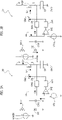
- FIG. 1 reproduces a circuit diagram of a conventional high-voltage startup (HVS) regulator designated 10 as a whole.
- HVS high-voltage startup
- Such a regulator is intended to provide a low voltage supply to a low-voltage section LV from a high voltage source VHVIN. It is noted that in various types of high-voltage power converters, such a high-voltage startup regulator may be used only during a power-on phase to be subsequently replaced by a more efficient supply source.
- a high-voltage startup regulator 10 as illustrated in Figure 1 comprises a "bypass" electronic switch MBP (a MOSFET transistor, for instance) able to withstand a high voltage applied across it.
- MBP a MOSFET transistor, for instance
- a MOSFET transistor is referred to herein as the switch MBP merely by way of example: other types of electronic switches (for instance, JFET, BJT, GaN) may be used as the switch MBP.
- the switch MBP is arranged with the current path therethrough (source-drain, in the case of a field-effect transistor such as a MOSFET) coupled intermediate an input node to which a high voltage VHVIN can be applied and the low-voltage section LV, which can be assumed to be referred to ground GND.
- source-drain in the case of a field-effect transistor such as a MOSFET
- the drain D of the MOSFET transistor MBP is connected to the high-voltage input node at VHVIN while the source S of the MOSFET transistor MBP supplies the low-voltage circuitry LV.
- a pull-up resistor RHV is used to bias the control node G (gate, in the case of a field-effect transistor such as a MOSFET) of the bypass switch MBP.
- the pull-up resistor RHV is arranged between the high-voltage input node at VHVIN and the gate G of MBP.
- a voltage clamp DZ (a zener diode, for instance) is arranged between the gate G of MBP and ground GND in order to limit the gate voltage range of MBP and define a highest (maximum) supply voltage for the low-voltage section LV.
- the input voltage is selected above the DZ voltage clamp.
- VHVIN MIN the lowest (minimum) input voltage
- MBP is a component having a gate bias current (I GATE )
- I GATE gate bias current
- a component "with leakage” may be an attractive option in monolithic or System in Package (SiP) arrangements: for instance, a high-voltage component with non-zero gate current may represent the only component available in a certain technological process and/or may represent an advanteous choice in view of specific design characteristics.
- SiP System in Package
- gallium-nitride (GaN) technology may be selected for the main switch in a converter in view of its improved static and dynamic performance in comparison with silicon-based power MOS transistors.
- Adding a dedicated component may be more expensive and complex.
- Using a bypass component MBP with a gate bias current I GATE forced to flow through RHV and then into the gate of MBP may provide a solution which is cost-effective and attractive (for instance, resulting in a monolithic solution with only one component available).
- Such an approach may otherwise exhibit various drawbacks: for instance, it may be hardly suited for use in very-low standby applications and/or may end up by providing undesirably expensive and complex solutions.
- One or more embodiments may address these issues adopting the approach illustrated in Figure 2 .
- circuitry designated 100 as a whole is coupled intermediate:
- the circuitry 100 comprises an electronic switch SW1 (a MOSFET transistor, for instance) with the current path therethrough (source-drain, in the case of a field-effect transistor such as a MOSFET) configured to connect - in response to the switch SW1 being "on", that is, conductive - the control node G of the "main” switch MBP to the node HV, and thus to the pull-up resistor RHV.
- SW1 a MOSFET transistor, for instance
- source-drain in the case of a field-effect transistor such as a MOSFET
- the circuitry 100 also comprises:
- Figures 3A and 3B are exemplary of possible operation of a regulator 10 as exemplified in Figure 2 .
- Figures 3A and 3B are exemplary of possible current flows in a regulator 10 as per the embodiments exemplified in Figure 2 :
- SW1 is assumed to be open (nonconductive) and no current I GATE can flow through RHV towards the node G and the voltage at the node HV follows VHVIN.
- the related information is stored by the latch 104 and SW1 is closed (that is, made conductive) via a signal SW1_ON being asserted.
- the charging of the capacitor CHV is used to pull-up the gate G of the switch MBP (exploiting the intrinsic gate-source capacitance, for instance) and a current I GATE is provided towards the node G.
- the charge pump 106 starts to supply current towards the node HV, drawing current from the source S of MBP (see Figure 3B ).
- the charge pump 106 thus provides the current I GATE and a current in excess of I GATE used to charge the capacitor CHV up to the voltage clamp of HV.
- the resistor RHV does not contribute appreciably to supplying the current I GATE and the voltage drop across RHV does not limit the lowest (minimum) input voltage, which is independent both of the resistance value of RHV value and of the intensity of I GATE .
- Figure 4 is a transistor-level diagram exemplary of a of a possible embodiment of the layout illustrated in Figure 2 based on a latched current comparator 1024, which is configured to facilitate having a current IHVtrig through the resistor RHV such that IHVtrig ⁇ I GATE .
- the latched comparator 1024 is based on a current mirror M3 including two transistors Q1 (in a diode-like configuration) and Q2 having current flow paths therethrough (emitter-collector, in the case of bipolar transistors as exemplified herein) that define respective current flow lines:
- the mutually connected bases of the transistors Q1 and Q2 are coupled to the node HV via the current flow path (source-drain, in the case of a MOSFET transistor as exemplified herein) through a further electronic switch M1 whose control node (gate in the case of a MOSFET transistor as exemplified herein) is coupled to the control node of the switch SW1 vie the line where the switching signal SW1_ON is applied with the parallel connection of a further voltage clamp DZUP and further pull-up resistor Rup coupling that line with the line/node HV.
- the charge pump 106 can be of any conventional type, such as Dickson, for instance, as exemplified in Figure 5 .
- Figure 6 comprises a set time diagrams exemplary of possible time behaviors, mapped against a common time (abscissa) scale of the following signals:
- FIG. 7 is a circuit diagram exemplary of the possible use of circuit 10 as discussed in the foregoing within the framework of a switched-mode power supply (that is an electronic power supply system that incorporates a switching regulator to convert electrical power efficiently).
- switched-mode power supply that is an electronic power supply system that incorporates a switching regulator to convert electrical power efficiently.
- FIG. 7 illustrates the possible use of embodiments in connection with a system in package (SIP) switched-mode power supply controller genarelly designated SMPS.
- SIP system in package
- Figure 7 exemplifeis the possible use of embodiments in switching power controllers (with a flyback topology in the - purely exemplary - case illustrated) integrating a main power switch PM (a power MOSFET transistor, for instance), with part of the circuit 10 included in the controller (for instance the clamp DZ, the bypass FET driver 100, and the switch MBP) while other components (such as the resistor RHV) may be external parts distinct from the circuit 100 (and 10).
- PM a power MOSFET transistor, for instance
- this may be the case of the source of the high-voltage VHVIN, represented in Figure 7 by a bridge rectifier BR supplied by an AC source ACin (a mains distribution grid, for instance) and having associated therewith a smoothing capacitor Cin intended to be coupled with the line or node VHVIN.
- a bridge rectifier BR supplied by an AC source ACin (a mains distribution grid, for instance) and having associated therewith a smoothing capacitor Cin intended to be coupled with the line or node VHVIN.
- the switch MBP is coupled to VHVIN (at its drain) indirectly, that is, via the primary winding of the converter transformer T.
- the low- voltage circuitry LV coupled to the switch MBP includes the supply portion og the SMPS controller, including a supply node VDD.
- the external network coupled to the node VDD is exemplified as a winding driving a rectifier diode and a smoothing capacitor Cvdd (not to be confused with the capacitor CHV discussed previously), provides an auxiliary power supply active during regulation.
- a current generator Icharge is illustrated as exemplary of the node VDD being charged with a controlled current.
- the current generator could be replaced with a diode exemplary of the fact that the auxiliary power supply and the power supply from the HVS circuit are mutually decoupled.
- the symbol PM in Figure 7 denotes a main switch of the switching converter.
- this may be of the same type of switch MBP (a GaN transistor, for instance).
- the reference 108 in Figure 7 denotes the logic control circuitry of the switch PM, which applies to the switch a PWM-modulated control signal via a driver 110.
- Figure 7 provides a fairly general representation of a switching controller: reference to a SMPS converter controller as made in Figure 7 is thus merely exemplary and not limiting of the embodiments.
- One or more embodiments may in fact be applied to flyback, boost topologies and other types of bypass regulators as a high-voltage startup current generator.
- One or more embodiments may provide various advantages such as, for instance:
- one or more embodiments remove a limitation of conventional high-voltage startup regulators employing as a bypass component an electronic switch having a (high) bias current.
- MOSFET transistor has been referred throughout as exemplary of the switch MBP, other types of electronic switches (for instance, JFET, BJT, GaN) may be used for the same purposes.
- Such a limitation is related to the voltage drop on a pull-up resistor (RHV, for instance) having one end used to bias the bypass switch gate such a resistor and other end connected at the main input voltage.
- RHV pull-up resistor
- One or more embodiments use a charge pump in order sustain the gate leakage current.
- Such a charge pump can be supplied by the transistor source and its activation involves pulling-up the gate of the bypass switch MBP.
- an electronic switch SW1 is interposed between the control node (gate, for instance) of the bypass switch MBP gate and the pull-up resistor.
- the switch is closed (by a latched comparator, for instance) as soon as the input voltage reaches a comparator threshold.
- the charge stored in a capacitor (CHV, for instance) connected between RHV and GND facilitates gate pull-up with the capability of supplying (and sustaining) both the consumption of the comparator/latch consumption and gate leakage, before the charge pump turning-on.
- CHV capacitor
- a circuit (for instance, 10) as exemplified herein may comprise: an electronic switch (for instance, MBP) having a current flow path (for instance, S, D) therethrough, the electronic switch configured to be coupled intermediate a high-voltage node (for instance, VHVIN) and low-voltage circuitry (for instance, LV), the electronic switch having a control node (for instance, G) configured to switch the electronic switch to a conductive state wherein the low-voltage circuitry is coupled to the high-voltage node.
- MBP electronic switch
- a current flow path for instance, S, D
- the electronic switch configured to be coupled intermediate a high-voltage node (for instance, VHVIN) and low-voltage circuitry (for instance, LV)
- the electronic switch having a control node (for instance, G) configured to switch the electronic switch to a conductive state wherein the low-voltage circuitry is coupled to the high-voltage node.
- a circuit as exemplified herein may further comprise a voltage-sensing node (for instance, HV) configured to be coupled to the high-voltage node via a pull-up resistor (for instance, RHV),
- HV voltage-sensing node
- RHV pull-up resistor
- a circuit as exemplified herein may comprise a charge capacitor (for instance, CHV) coupled (for instance, via HV) to the charge pump to be charged thereby via charge in excess of the charge pumped to the control node of the electronic switch.
- a charge capacitor for instance, CHV
- HV charge pump
- the charge pump is coupled to the voltage-sensing node and configured to pump therein charge sourced from the current flow-path of the electronic switch.
- a circuit as exemplified herein may comprise a latch circuit (for instance, 104) intermediate the comparator and the further electronic switch to latch therein said switch-on signal in response to the voltage at said voltage-sensing node reaching said threshold.
- a latch circuit for instance, 104
- the voltage-sensing node is configured to be coupled to the high-voltage node intermediate said pull-up resistor (for instance, RHV) and a voltage clamp (for instance, DZ) referred to ground (for instance, GND) configured to clamp to a limit value the voltage at the voltage-sensing node.
- a voltage clamp for instance, DZ
- ground for instance, GND
- the electronic switch for instance, MBP
- the electronic switch has a first node (for instance, D) configured to be coupled to the high-voltage node (for instance, VHVIN) and a second node (for instance, S) configured to be coupled to the low-voltage circuitry (for instance, LV), and wherein the charge pump is coupled to the current flow-path of the electronic switch at the second node (for instance, S).
- the electronic switch and the further electronic switch may comprise field-effect transistors, optionally MOSFET transistors.
- a power supply system as exemplified herein may comprise:
- a method as exemplified herein may comprise supplying low-voltage circuitry (for instance, LV) a from a high-voltage source (for instance, BR, Cin) by:
Landscapes
- Engineering & Computer Science (AREA)
- Power Engineering (AREA)
- Physics & Mathematics (AREA)
- Electromagnetism (AREA)
- General Physics & Mathematics (AREA)
- Radar, Positioning & Navigation (AREA)
- Automation & Control Theory (AREA)
- Dc-Dc Converters (AREA)
- Continuous-Control Power Sources That Use Transistors (AREA)
- Stereo-Broadcasting Methods (AREA)
- Input Circuits Of Receivers And Coupling Of Receivers And Audio Equipment (AREA)
Abstract
Description
- The description relates to regulator circuits.
- One or more embodiments can be applied to driving bypass field-effect transistors in high-voltage startup regulators as used in a variety of products.
- These products may include, for instance, chargers/adapters, home appliances such as refrigerators or TVs, industrial machinery, telecom apparatus and so on.
- Regulator circuits such as high-voltage startup (HVS) regulators may include a bypass transistor (a MOSFET transistor, for instance), a pull-up resistor used to bias the gate of the bypass transistor, as well as a voltage clamp connected between the gate of the bypass transistor and ground in order to limit the gate voltage range and define a maximum supply voltage output.
- Such an approach may exhibit certain limitations in terms of power consumption, application input range, and cost.
- For instance, in low-power applications, a constraint may be placed on the lowest (minimum) resistance value for the pull-up resistor.
- Under those circumstances, achieving a trade-off between such a constraint on the minimum resistance value for the pull-up resistor and the lowest (minimum) high-voltage input may become critical, while on the other hand a bypass component with a gate bias current still represents an attractive, cost-effective solution.
- An object of one or more embodiments is to contribute in addressing the issues discussed in the foregoing.
- According to one or more embodiments, such an object can be achieved by means of a circuit having the features set forth in the claims that follow.
- One or more embodiments may relate to a corresponding system. A switched-mode power supply (SMPS) system may be exemplary of such a system.
- One or more embodiments may relate to a corresponding method.
- The claims are an integral part of the technical teaching on the embodiments as provided herein.
- One or more embodiments may provide a cost-effective solution, primarily in comparison with the use of a dedicated HV-MOS with no gate leakage.
- One or more embodiments may use a charge pump to sustain the gate leakage current. Such a charge pump can be supplied by a transistor source and its activation may thus involve pulling-up the gate of the bypass transistor.
- In one or more embodiments, an (electronic) switch may be interposed between the gate and the pull-up resistor.
- The switch can be closed (that is, made conductive) by a latched comparator in response to the input voltage reaching (that is, rising up to) a comparator threshold.
- The charge stored in a capacitor intermediate (between) the pull-up resistor (RHV) and ground facilitates pulling-up the gate with the capability of providing both supply energy as consumed by the comparator/latch and supporting gate leakage, before charge pump turn-on.
- One or more embodiments can effectively address certain limitations in terms of power consumption, application input range, and cost.
- The possible presence of an embedded charge pump may result in a negative current detected on a high-voltage pin when the high voltage startup regulator is active.
- One or more embodiments will now be described, by way of example only, with reference to the annexed figures, wherein:
-
Figure 1 is a block diagram exemplary of a conventional high-voltage startup (HVS) regulator; -
Figure 2 is a block diagram exemplary of a high-voltage startup (HVS) regulator according to embodiments as per the instant description; -
Figures 3A and 3B are block diagrams exemplary of possible operation of a regulator as illustrated inFigure 2 ; -
Figure 4 is a transistor-level representation of possible embodiments as per the instant description; -
Figure 5 is a circuit diagram of a possible implementation of a component (charge pump) illustrated in Fguire 4; -
Figure 6 comprises a set of time diagram illustrative of a possible time behavior of particular signals which may occur a in a regulator according to embodiments as per the instant description; and -
Figure 7 is a circuit diagram exemplary of the possible use of a regulator according to embodiments as per the instant description within the framework of a switched-mode power supply system. - In the ensuing description one or more specific details are illustrated, aimed at providing an in-depth understanding of examples of embodiments of this description. The embodiments may be obtained without one or more of the specific details, or with other methods, components, materials, etc. In other cases, known structures, materials, or operations are not illustrated or described in detail so that certain aspects of embodiments will not be obscured.
- Reference to "an embodiment" or "one embodiment" in the framework of the present description is intended to indicate that a particular configuration, structure, or characteristic described in relation to the embodiment is comprised in at least one embodiment. Hence, phrases such as "in an embodiment" or "in one embodiment" that may be present in one or more points of the present description do not necessarily refer to one and the same embodiment.
- Moreover, particular conformations, structures, or characteristics may be combined in any adequate way in one or more embodiments.
- The headings/references used herein are provided merely for convenience and hence do not define the extent of protection or the scope of the embodiments.
- By way of introduction to the instant detailed description, reference may be had to
Figure 1 , which reproduces a circuit diagram of a conventional high-voltage startup (HVS) regulator designated 10 as a whole. - Such a regulator is intended to provide a low voltage supply to a low-voltage section LV from a high voltage source VHVIN. It is noted that in various types of high-voltage power converters, such a high-voltage startup regulator may be used only during a power-on phase to be subsequently replaced by a more efficient supply source.
- A high-
voltage startup regulator 10 as illustrated inFigure 1 comprises a "bypass" electronic switch MBP (a MOSFET transistor, for instance) able to withstand a high voltage applied across it. - In that respect, those of skill in the art will appreciate that a MOSFET transistor is referred to herein as the switch MBP merely by way of example: other types of electronic switches (for instance, JFET, BJT, GaN) may be used as the switch MBP.
- As illustrated in
Figure 1 , the switch MBP is arranged with the current path therethrough (source-drain, in the case of a field-effect transistor such as a MOSFET) coupled intermediate an input node to which a high voltage VHVIN can be applied and the low-voltage section LV, which can be assumed to be referred to ground GND. - As illustrated in
Figure 1 , the drain D of the MOSFET transistor MBP is connected to the high-voltage input node at VHVIN while the source S of the MOSFET transistor MBP supplies the low-voltage circuitry LV. - A pull-up resistor RHV is used to bias the control node G (gate, in the case of a field-effect transistor such as a MOSFET) of the bypass switch MBP.
- As illustrated, the pull-up resistor RHV is arranged between the high-voltage input node at VHVIN and the gate G of MBP.
- A voltage clamp DZ (a zener diode, for instance) is arranged between the gate G of MBP and ground GND in order to limit the gate voltage range of MBP and define a highest (maximum) supply voltage for the low-voltage section LV.
- In order to reach this voltage value, the input voltage is selected above the DZ voltage clamp.
- In low-power applications, a constraint on the minimum value of the resistance of RHV is set in order to limit waste of power. Another specification is the lowest (minimum) input voltage (VHVINMIN) for which the high-voltage regulator is expected to be capable of supplying the downstream circuits.
- Assuming MBP is a component having a gate bias current (IGATE) a certain voltage drop on RHV may exist which establishes a judicious trade-off between the constraint on the minimum RHV and the minimum high-voltage input.
- A problem arises when this trade-off cannot be satisfactorily reached.
- For instance, with RHV=10MQ and IGATE =10µA, the minimum input voltage is above 100V.
- In principle, using a lower resistance value for RHV may be considered, to the point of even dispensing with such resistance. It is otherwise noted that the minimum value for that resistance is related to a desirably reduced stand-by consumption, which results in a design constraint.
- Also, using a component "with leakage" may be an attractive option in monolithic or System in Package (SiP) arrangements: for instance, a high-voltage component with non-zero gate current may represent the only component available in a certain technological process and/or may represent an advanteous choice in view of specific design characteristics.
- For instance, gallium-nitride (GaN) technology may be selected for the main switch in a converter in view of its improved static and dynamic performance in comparison with silicon-based power MOS transistors. Adding a dedicated component (a SIP with a dedicated die and/or process) may be more expensive and complex.
- Using a bypass component MBP with a gate bias current IGATE forced to flow through RHV and then into the gate of MBP may provide a solution which is cost-effective and attractive (for instance, resulting in a monolithic solution with only one component available). Such an approach may otherwise exhibit various drawbacks: for instance, it may be hardly suited for use in very-low standby applications and/or may end up by providing undesirably expensive and complex solutions.
- One or more embodiments may address these issues adopting the approach illustrated in
Figure 2 . - In that respect, it will be appreciated that:
- unless the context indicates otherwise, like parts or elements are indicated throughout the annexed figures with like reference symbols, and a detailed description will not be repeated for each and every figure for brevity; consequently, parts or elements already discussed in connection with
Figure 1 are indicated throughout the annexed figures with like reference symbols and will not be not discussed again; - for the sake of simplicity and ease of understanding, a same designation may be used herein to indicate both a node or line in a circuit and a signal (voltage, current, for instance) occurring at that node or line: see, for instance, VHVIN, as already introduced previously;
- various components illustrated and discussed for ease of explanation (the source of the high-voltage VHVIN and the low-voltage circuitry LV, for instance) may be distinct elements from the embodiments.
- In one or more embodiments as illustrated in
Figure 2 , circuitry designated 100 as a whole is coupled intermediate: - a node HV intermediate the resistor RHV and the voltage clamp DZ, and
- the control node G (here, gate) of the switch MBP.
- As illustrated, the
circuitry 100 comprises an electronic switch SW1 (a MOSFET transistor, for instance) with the current path therethrough (source-drain, in the case of a field-effect transistor such as a MOSFET) configured to connect - in response to the switch SW1 being "on", that is, conductive - the control node G of the "main" switch MBP to the node HV, and thus to the pull-up resistor RHV. - As illustrated, the
circuitry 100 also comprises: - a capacitor CHV interposed between the node HV and ground (that is, in parallel to the voltage clamp DZ;
- a
comparator 102 configured to sense the voltage at the node HV (that is, the voltage across the capacitor CHV) with a threshold VTH (generated in a manner known per se to those of skill in the art); - a
latch circuit 104 configured to latch the output of thecomparator 102 and to control via its output the status of the switch SW1; and - a
charge pump 106 interposed between a node S (source, for instance, in the case of a field-effect transistor such as MOSFET) intermediate the switch MBP and the low-voltage section LV and the node HV, thecharge pump 106 having the purpose of sustaining a bias current through the switch MBP while avoiding an undesired voltage drop on RHV. -
Figures 3A and 3B are exemplary of possible operation of aregulator 10 as exemplified inFigure 2 . - Once again, unless the context indicates otherwise, parts or elements already discussed in connection with
Figures 1 and 2 are indicated inFigures 3A and 3B with like reference symbols and will not be not described again for brevity. - More specifically,
Figures 3A and 3B are exemplary of possible current flows in aregulator 10 as per the embodiments exemplified inFigure 2 : - before the
charge pump 106 is turned on (Figure 3A ), - after the
charge pump 106 is turned on (Figure 3B ) . - At power-on, SW1 is assumed to be open (nonconductive) and no current IGATE can flow through RHV towards the node G and the voltage at the node HV follows VHVIN.
- In response to the voltage at the node HV reaching the threshold VTH of the comparator 102 (20 V, by way of example), the related information is stored by the
latch 104 and SW1 is closed (that is, made conductive) via a signal SW1_ON being asserted. - In this phase the charging of the capacitor CHV is used to pull-up the gate G of the switch MBP (exploiting the intrinsic gate-source capacitance, for instance) and a current IGATE is provided towards the node G.
- When the voltage on the source S of MBP is enough (that is, it exceeds a lower threshold as desired), the
charge pump 106 starts to supply current towards the node HV, drawing current from the source S of MBP (seeFigure 3B ). - The
charge pump 106 thus provides the current IGATE and a current in excess of IGATE used to charge the capacitor CHV up to the voltage clamp of HV. - That is, during high-voltage regulator operation, the resistor RHV does not contribute appreciably to supplying the current IGATE and the voltage drop across RHV does not limit the lowest (minimum) input voltage, which is independent both of the resistance value of RHV value and of the intensity of IGATE.
-
Figure 4 is a transistor-level diagram exemplary of a of a possible embodiment of the layout illustrated inFigure 2 based on a latched current comparator 1024, which is configured to facilitate having a current IHVtrig through the resistor RHV such that IHVtrig <<< IGATE. - Once again, unless the context indicates otherwise, parts or elements already discussed in connection with
Figures 1, 2 and3A and 3B are indicated inFigure 4 with like reference symbols and will not be not described again for brevity. - Essentially, the latched comparator 1024 is based on a current mirror M3 including two transistors Q1 (in a diode-like configuration) and Q2 having current flow paths therethrough (emitter-collector, in the case of bipolar transistors as exemplified herein) that define respective current flow lines:
- between the node HV and ground GND via the current clamp DZ (transistor Q1), and
- between the control node (gate) of the switch SW1 and ground GND (transistor Q2).
- The mutually connected bases of the transistors Q1 and Q2 are coupled to the node HV via the current flow path (source-drain, in the case of a MOSFET transistor as exemplified herein) through a further electronic switch M1 whose control node (gate in the case of a MOSFET transistor as exemplified herein) is coupled to the control node of the switch SW1 vie the line where the switching signal SW1_ON is applied with the parallel connection of a further voltage clamp DZUP and further pull-up resistor Rup coupling that line with the line/node HV.
- In
Figure 4 , the main currents before start-up are indicated in continuous lines. Dashes lines denote main currents at startup and chain lines denote the main currents in steady state after activation of thecharge pump 106. - The
charge pump 106 can be of any conventional type, such as Dickson, for instance, as exemplified inFigure 5 . -
Figure 6 comprises a set time diagrams exemplary of possible time behaviors, mapped against a common time (abscissa) scale of the following signals: - the "high" voltage VHVIN (continuous line)
- the signal SW1_ON (dashed line)
- the voltage at node HV (chain line)
- the voltage at node G (mixed dash and cross line--+--+, which finally superposes with the voltage at node HV
- the voltage S ((mixed dash and double-cross line--++--++--.
- The diagrams of
Figure 6 are exemplary of a possible start-up sequence including events designated with numbers from 1 to 5 such as: - 1 - the node HV reaches the threshold VTH that triggers the closing of SW1 (at a time tstart);
- 2 - the intrinsic capacitance at the node G is charged via charge sharing with the capacitance CHV;
- 3 - charge sharing causes a voltage drop on the node HV until the voltage at that node equals the voltage on the G node (at a time tcharge after tstart);
- 4 - the S node follows the node G with a voltage drop therebetween close to the threshold of MBP and MBP starts supplying the charge pump 106 (time tstartCHP);
- 5 - the
charge pump 106 re-charges the capacitor CHV up to the voltage clamp. -
Figure 7 is a circuit diagram exemplary of the possible use ofcircuit 10 as discussed in the foregoing within the framework of a switched-mode power supply (that is an electronic power supply system that incorporates a switching regulator to convert electrical power efficiently). - Once again, unless the context indicates otherwise, parts or elements already discussed in connection with the previous figures are indicated in
Figure 7 with like reference symbols and will not be not described again for brevity. -
Figure 7 illustrates the possible use of embodiments in connection with a system in package (SIP) switched-mode power supply controller genarelly designated SMPS. -
Figure 7 exemplifeis the possible use of embodiments in switching power controllers (with a flyback topology in the - purely exemplary - case illustrated) integrating a main power switch PM (a power MOSFET transistor, for instance), with part of thecircuit 10 included in the controller (for instance the clamp DZ, thebypass FET driver 100, and the switch MBP) while other components (such as the resistor RHV) may be external parts distinct from the circuit 100 (and 10). - For instance, this may be the case of the source of the high-voltage VHVIN, represented in
Figure 7 by a bridge rectifier BR supplied by an AC source ACin (a mains distribution grid, for instance) and having associated therewith a smoothing capacitor Cin intended to be coupled with the line or node VHVIN. - In an arrangement as exemplified in
Figure 7 , in the place of being coupled to VHVIN directly as discussed previously, the switch MBP is coupled to VHVIN (at its drain) indirectly, that is, via the primary winding of the converter transformer T. - In an arrangement as exemplified in
Figure 7 , the low- voltage circuitry LV coupled to the switch MBP (here at the source) includes the supply portion og the SMPS controller, including a supply node VDD. - The external network coupled to the node VDD is exemplified as a winding driving a rectifier diode and a smoothing capacitor Cvdd (not to be confused with the capacitor CHV discussed previously), provides an auxiliary power supply active during regulation. A current generator Icharge is illustrated as exemplary of the node VDD being charged with a controlled current. The current generator could be replaced with a diode exemplary of the fact that the auxiliary power supply and the power supply from the HVS circuit are mutually decoupled.
- The symbol PM in
Figure 7 denotes a main switch of the switching converter. Advantageously, this may be of the same type of switch MBP (a GaN transistor, for instance). - The
reference 108 inFigure 7 denotes the logic control circuitry of the switch PM, which applies to the switch a PWM-modulated control signal via adriver 110. - This may occur in any conventional manner known to those of skill in the art. It will be otherwise appreciated that
Figure 7 provides a fairly general representation of a switching controller: reference to a SMPS converter controller as made inFigure 7 is thus merely exemplary and not limiting of the embodiments. - One or more embodiments may in fact be applied to flyback, boost topologies and other types of bypass regulators as a high-voltage startup current generator.
- One or more embodiments may provide various advantages such as, for instance:
- power consumption is reduced,
- limits on the application input range are removed,
- a cost-effective solution is provided in comparison with the use of dedicated HV-MOS that has no gate leakage,
- gate leakage current flowing in the resistor RHV at power-on is avoided via the switch SW1,
- the comparator and latch circuitry (that is 102, 104, 1024) exhibits a low consumption before the switch SW1 is turned-on,
- a simple charge pump circuit is used to sustain bypass FET gate leakage.
- Briefly, one or more embodiments remove a limitation of conventional high-voltage startup regulators employing as a bypass component an electronic switch having a (high) bias current.
- In that respect, it is again noted that, while a MOSFET transistor has been referred throughout as exemplary of the switch MBP, other types of electronic switches (for instance, JFET, BJT, GaN) may be used for the same purposes.
- Such a limitation is related to the voltage drop on a pull-up resistor (RHV, for instance) having one end used to bias the bypass switch gate such a resistor and other end connected at the main input voltage.
- One or more embodiments use a charge pump in order sustain the gate leakage current.
- Such a charge pump can be supplied by the transistor source and its activation involves pulling-up the gate of the bypass switch MBP.
- In one or more embodiments an electronic switch SW1 is interposed between the control node (gate, for instance) of the bypass switch MBP gate and the pull-up resistor. The switch is closed (by a latched comparator, for instance) as soon as the input voltage reaches a comparator threshold.
- The charge stored in a capacitor (CHV, for instance) connected between RHV and GND facilitates gate pull-up with the capability of supplying (and sustaining) both the consumption of the comparator/latch consumption and gate leakage, before the charge pump turning-on.
- Briefly, a circuit (for instance, 10) as exemplified herein may comprise:
an electronic switch (for instance, MBP) having a current flow path (for instance, S, D) therethrough, the electronic switch configured to be coupled intermediate a high-voltage node (for instance, VHVIN) and low-voltage circuitry (for instance, LV), the electronic switch having a control node (for instance, G) configured to switch the electronic switch to a conductive state wherein the low-voltage circuitry is coupled to the high-voltage node. - A circuit as exemplified herein may further comprise a voltage-sensing node (for instance, HV) configured to be coupled to the high-voltage node via a pull-up resistor (for instance, RHV),
- a further electronic switch (for instance, SW1) intermediate the voltage-sensing node and the control node of the electronic switch, the further electronic switch switchable to a conductive state to couple the voltage-sensing node and the control node of the electronic switch in response to a switch-on signal (for instance, SW1_ON) being asserted,
- a comparator (for instance, 102) coupled to the voltage-sensing node and a threshold, the comparator configured to compare a voltage at said voltage-sensing node with the threshold and cause the switch-on signal to be asserted in response to the voltage at said voltage-sensing node reaching said threshold, and
- a charge pump (for instance, 106) coupled to the current flow-path of the electronic switch and configured to be activated with the further electronic switch switched to the conductive state to pump electric charge (for instance, IGATE) from the current flow-path of the electronic switch to the control node of the electronic switch via the further electronic switch switched to the conductive state.
- A circuit as exemplified herein may comprise a charge capacitor (for instance, CHV) coupled (for instance, via HV) to the charge pump to be charged thereby via charge in excess of the charge pumped to the control node of the electronic switch.
- In a circuit as exemplified herein, the charge pump is coupled to the voltage-sensing node and configured to pump therein charge sourced from the current flow-path of the electronic switch.
- A circuit as exemplified herein may comprise a latch circuit (for instance, 104) intermediate the comparator and the further electronic switch to latch therein said switch-on signal in response to the voltage at said voltage-sensing node reaching said threshold.
- In a circuit as exemplified herein, the voltage-sensing node is configured to be coupled to the high-voltage node intermediate said pull-up resistor (for instance, RHV) and a voltage clamp (for instance, DZ) referred to ground (for instance, GND) configured to clamp to a limit value the voltage at the voltage-sensing node.
- In a circuit as exemplified herein, the electronic switch (for instance, MBP) has a first node (for instance, D) configured to be coupled to the high-voltage node (for instance, VHVIN) and a second node (for instance, S) configured to be coupled to the low-voltage circuitry (for instance, LV), and wherein the charge pump is coupled to the current flow-path of the electronic switch at the second node (for instance, S).
- In a circuit as exemplified herein, the electronic switch and the further electronic switch may comprise field-effect transistors, optionally MOSFET transistors.
- A power supply system as exemplified herein may comprise:
- a high-voltage source (for instance, BR, Cin),
- a circuit as exemplified herein (for instance, 10) having said high-voltage node (for instance, VHVIN) coupled to the high-voltage source (for instance, BR, Cin), and
- low-voltage circuitry (for instance, LV) coupled (for instance, at S) to the electronic switch wherein the low-voltage circuitry is coupled to the high-voltage node in response to the electronic switch being switched to a conductive state.
- A method as exemplified herein may comprise supplying low-voltage circuitry (for instance, LV) a from a high-voltage source (for instance, BR, Cin) by:
- coupling intermediate the high-voltage source and the low-voltage circuitry an electronic switch (for instance, MBP) having a current flow path (for instance, S, D) therethrough and a control node (for instance, G),
- switching the electronic switch to a conductive state via the control node thereof to couple the low-voltage circuitry to the high-voltage source,
- coupling a voltage-sensing node to the high-voltage source via a pull-up resistor (for instance, RHV),
- providing a further electronic switch (for instance, SW1) intermediate the voltage-sensing node and the control node of the electronic switch,
- switching (for instance, SW1_ON) the further electronic switch to a conductive state to couple the voltage-sensing node and the control node of the electronic switch in response to the voltage at said voltage-sensing node reaching a threshold (for instance, VTH), and
- providing a charge pump (for instance, 106) coupled to the current flow-path of the electronic switch, and
- activating the charge pump with the further electronic switch switched to the conductive state to pump electric charge (for instance, IGATE) from the current flow-path of the electronic switch to the control node of the electronic switch via the further electronic switch (SW1) switched to the conductive state.
- Without prejudice to the underlying principles, the details and embodiments may vary, even significantly, with respect to what has been described by way of example only without departing from the extent of protection.
- The extent of protection is determined by the annexed claims.
Claims (9)
- A circuit (10), comprising:an electronic switch (MBP) having a current flow path (S, D) therethrough, the electronic switch (MBP) configured to be coupled intermediate a high-voltage node (VHVIN) and low-voltage circuitry (LV), the electronic switch (MBP) having a control node (G) configured to switch the electronic switch (MBP) to a conductive state wherein the low-voltage circuitry (LV) is coupled to the high-voltage node (VHVIN),a voltage-sensing node (HV) configured to be coupled to the high-voltage node (VHVIN) via a pull-up resistor (RHV),a further electronic switch (SW1) intermediate the voltage-sensing node (HV) and the control node (G) of the electronic switch (MBP), the further electronic switch (SW1) switchable to a conductive state to couple the voltage-sensing node (HV) and the control node (G) of the electronic switch (MBP) in response to a switch-on signal (SW1_ON) being asserted,a comparator (102) coupled to the voltage-sensing node (HV) and a threshold (VTH), the comparator (102) configured to compare a voltage at said voltage-sensing node (HV) with the threshold (VTH) and cause (104) the switch-on signal (SW1_ON) to be asserted in response to the voltage at said voltage-sensing node (HV) reaching said threshold (VTH), anda charge pump (106) coupled to the current flow-path of the electronic switch (MBP) and configured to be activated with the further electronic switch (SW1) switched to the conductive state to pump electric charge (IGATE) from the current flow-path of the electronic switch (MBP) to the control node (G) of the electronic switch (MBP) via the further electronic switch (SW1) switched to the conductive state.
- The circuit (10) of claim 1, comprising a charge capacitor (CHV) coupled (HV) to the charge pump (106) to be charged thereby via charge in excess of the charge (IGATE) pumped to the control node (G) of the electronic switch (MBP).
- The circuit (10) of claim 1 or claim 2, wherein the charge pump (106) is coupled to the voltage-sensing node (HV) and configured to pump therein charge sourced from the current flow-path of the electronic switch (MBP) .
- The circuit (10) of any of the previous claims, comprising a latch circuit (104) intermediate the comparator (102) and the further electronic switch (SW1) to latch therein said switch-on signal (SW1_ON) in response to the voltage at said voltage-sensing node (HV) reaching said threshold (VTH).
- The circuit (10) of any of the previous claims, wherein the voltage-sensing node (HV) is configured to be coupled to the high-voltage node (VHVIN) intermediate said pull-up resistor (RHV) and a voltage clamp (DZ) referred to ground (GND) configured to clamp to a limit value the voltage at the voltage-sensing node (HV).
- The circuit (10) of any of the previous claims, wherein the electronic switch (MBP) has a first node (D) configured to be coupled to the high-voltage node (VHVIN) and a second node (S) configured to be coupled to the low-voltage circuitry (LV), and wherein the charge pump (106) is coupled to the current flow-path of the electronic switch (MBP) at the second node (S).
- The circuit (10) of any of the previous claims, wherein the electronic switch (MBP) and the further electronic switch (SW1) comprise field-effect transistors, preferably MOSFET transistors.
- A power supply system, comprising:a high-voltage source (BR, Cin),a circuit (10) according to any of the previous claims having said high-voltage node (VHVIN) coupled to the high-voltage source (BR, Cin), andlow-voltage circuitry (LV) coupled (S) to the electronic switch (MBP) wherein the low-voltage circuitry (LV) is coupled to the high-voltage node (VHVIN) in response to the electronic switch (MBP) being switched to a conductive state.
- A method of supplying low-voltage circuitry (LV) a from a high-voltage source (BR, Cin), the method comprising:coupling intermediate the high-voltage source (VHVIN; BR, Cin) and the low-voltage circuitry (LV) an electronic switch (MBP) having a current flow path (S, D) therethrough and a control node (G),switching the electronic switch (MBP) to a conductive state via the control node (G) thereof to couple the low-voltage circuitry (LV) to the high-voltage source (VHVIN; BR, Cin),coupling a voltage-sensing node (HV) to the high-voltage source (VHVIN; BR, Cin) via a pull-up resistor (RHV),providing a further electronic switch (SW1) intermediate the voltage-sensing node (HV) and the control node (G) of the electronic switch (MBP),switching (SW1_ON) the further electronic switch (SW1) to a conductive state to couple the voltage-sensing node (HV) and the control node (G) of the electronic switch (MBP) in response to the voltage at said voltage-sensing node (HV) reaching a threshold (VTH), andproviding a charge pump (106) coupled to the current flow-path of the electronic switch (MBP), andactivating the charge pump (106) with the further electronic switch (SW1) switched to the conductive state to pump electric charge (IGATE) from the current flow-path of the electronic switch (MBP) to the control node (G) of the electronic switch (MBP) via the further electronic switch (SW1) switched to the conductive state.
Applications Claiming Priority (1)
| Application Number | Priority Date | Filing Date | Title |
|---|---|---|---|
| IT102021000002798A IT202100002798A1 (en) | 2021-02-09 | 2021-02-09 | REGULATOR CIRCUIT, CORRESPONDING SYSTEM AND PROCEDURE |
Publications (2)
| Publication Number | Publication Date |
|---|---|
| EP4040678A1 true EP4040678A1 (en) | 2022-08-10 |
| EP4040678B1 EP4040678B1 (en) | 2024-11-06 |
Family
ID=75439379
Family Applications (1)
| Application Number | Title | Priority Date | Filing Date |
|---|---|---|---|
| EP21215447.0A Active EP4040678B1 (en) | 2021-02-09 | 2021-12-17 | Regulator circuit, corresponding system and method |
Country Status (4)
| Country | Link |
|---|---|
| US (2) | US11791728B2 (en) |
| EP (1) | EP4040678B1 (en) |
| CN (2) | CN217739800U (en) |
| IT (1) | IT202100002798A1 (en) |
Families Citing this family (3)
| Publication number | Priority date | Publication date | Assignee | Title |
|---|---|---|---|---|
| IT202100002798A1 (en) * | 2021-02-09 | 2022-08-09 | St Microelectronics Srl | REGULATOR CIRCUIT, CORRESPONDING SYSTEM AND PROCEDURE |
| IT202300015036A1 (en) * | 2023-07-18 | 2025-01-18 | St Microelectronics Int Nv | STRESS CALIBRATION PROCEDURE, CORRESPONDING ELECTRONIC DEVICE AND VEHICLE |
| CN117459042B (en) * | 2023-12-22 | 2024-03-08 | 瓴芯电子科技(无锡)有限公司 | Power switch chip, method for detecting output end state of power switch chip and electronic equipment |
Citations (4)
| Publication number | Priority date | Publication date | Assignee | Title |
|---|---|---|---|---|
| US20090179691A1 (en) * | 2008-01-10 | 2009-07-16 | Micron Technology, Inc. | Voltage generator circuit |
| US20110316509A1 (en) * | 2010-06-25 | 2011-12-29 | Hangzhou Silergy Semiconductor Technology LTD | Start-up circuit and method thereof |
| US9742262B1 (en) * | 2016-05-06 | 2017-08-22 | Bel Fuse (Macao Commerical Offshore) Limited | Switching power supply startup circuit with normally on device providing startup charging current |
| US20200076190A1 (en) * | 2018-09-03 | 2020-03-05 | Stmicroelectronics S.R.L. | Supply protection circuit and corresponding device |
Family Cites Families (16)
| Publication number | Priority date | Publication date | Assignee | Title |
|---|---|---|---|---|
| US6426614B1 (en) * | 2000-08-24 | 2002-07-30 | Research In Motion Limited | Boot-strapped current switch |
| DE10051936B4 (en) * | 2000-10-19 | 2004-10-14 | Infineon Technologies Ag | Voltage pump with switch-on control |
| JP4278572B2 (en) * | 2004-06-16 | 2009-06-17 | 矢崎総業株式会社 | Semiconductor switch control device |
| CN100552592C (en) * | 2004-07-09 | 2009-10-21 | 莫赛德技术公司 | System and method for minimizing static leakage in integrated circuits |
| US7787264B2 (en) * | 2007-07-25 | 2010-08-31 | System General Corp. | Apparatus to provide synchronous rectifying circuit for flyback power converters |
| US9143033B2 (en) * | 2010-11-30 | 2015-09-22 | Taiwan Semiconductor Manufacturing Company, Ltd. | Hysteretic power converter with calibration circuit |
| EP2518878B1 (en) * | 2011-04-29 | 2018-10-17 | STMicroelectronics S.r.l. | DC-DC converter, method for operating the DC-DC converter, environmental energy harvesting system comprising the DC-DC converter, and apparatus comprising the energy harvesting system |
| FR2975512B1 (en) * | 2011-05-17 | 2013-05-10 | St Microelectronics Rousset | METHOD AND DEVICE FOR GENERATING AN ADJUSTABLE REFERENCE VOLTAGE OF BAND PROHIBITED |
| KR20130066266A (en) * | 2011-12-12 | 2013-06-20 | 한국전자통신연구원 | Voltage regulator with improved load regulation and voltage regulating method |
| US9203307B2 (en) * | 2012-10-31 | 2015-12-01 | Cree, Inc. | Power converter with bias voltage regulation circuit |
| US9231472B2 (en) * | 2014-04-11 | 2016-01-05 | Infineon Technologies Austria Ag | System and method for a switched-mode power supply |
| US9520769B2 (en) * | 2014-04-30 | 2016-12-13 | Stmicroelectronics S.R.L. | Wake up management circuit for a switching converter and related wake up method |
| SG11201701477QA (en) * | 2014-08-26 | 2017-03-30 | Toshiba Kk | Voltage generation circuit |
| JP6510288B2 (en) * | 2015-03-30 | 2019-05-08 | ローム株式会社 | Charge pump circuit |
| US11139811B2 (en) * | 2019-04-30 | 2021-10-05 | Stmicroelectronics S.R.L. | Driver circuit, corresponding device and system |
| IT202100002798A1 (en) * | 2021-02-09 | 2022-08-09 | St Microelectronics Srl | REGULATOR CIRCUIT, CORRESPONDING SYSTEM AND PROCEDURE |
-
2021
- 2021-02-09 IT IT102021000002798A patent/IT202100002798A1/en unknown
- 2021-12-17 EP EP21215447.0A patent/EP4040678B1/en active Active
-
2022
- 2022-01-28 US US17/588,065 patent/US11791728B2/en active Active
- 2022-02-08 CN CN202220255702.4U patent/CN217739800U/en not_active Withdrawn - After Issue
- 2022-02-08 CN CN202210119137.3A patent/CN114911296B/en active Active
-
2023
- 2023-08-30 US US18/458,940 patent/US12294302B2/en active Active
Patent Citations (4)
| Publication number | Priority date | Publication date | Assignee | Title |
|---|---|---|---|---|
| US20090179691A1 (en) * | 2008-01-10 | 2009-07-16 | Micron Technology, Inc. | Voltage generator circuit |
| US20110316509A1 (en) * | 2010-06-25 | 2011-12-29 | Hangzhou Silergy Semiconductor Technology LTD | Start-up circuit and method thereof |
| US9742262B1 (en) * | 2016-05-06 | 2017-08-22 | Bel Fuse (Macao Commerical Offshore) Limited | Switching power supply startup circuit with normally on device providing startup charging current |
| US20200076190A1 (en) * | 2018-09-03 | 2020-03-05 | Stmicroelectronics S.R.L. | Supply protection circuit and corresponding device |
Also Published As
| Publication number | Publication date |
|---|---|
| IT202100002798A1 (en) | 2022-08-09 |
| CN217739800U (en) | 2022-11-04 |
| US20230412080A1 (en) | 2023-12-21 |
| CN114911296B (en) | 2026-03-31 |
| EP4040678B1 (en) | 2024-11-06 |
| US12294302B2 (en) | 2025-05-06 |
| US20220255428A1 (en) | 2022-08-11 |
| CN114911296A (en) | 2022-08-16 |
| US11791728B2 (en) | 2023-10-17 |
Similar Documents
| Publication | Publication Date | Title |
|---|---|---|
| US12294302B2 (en) | Regulator circuit, corresponding system and method | |
| US8487664B2 (en) | System and method for driving a switch | |
| US8558584B2 (en) | System and method for bootstrapping a switch driver | |
| US7894219B2 (en) | Method and apparatus of low current startup circuit for switching mode power supplies | |
| CN104170254B (en) | System and apparatus for protecting a driver circuit of a gate of a gallium nitride field effect transistor | |
| US6563726B1 (en) | Synchronous bridge rectifier | |
| CN104242612B (en) | Method and system for driving transistor | |
| US8310281B2 (en) | System and method for driving a cascode switch | |
| CN102111070A (en) | Standby current-reduced regulator over-voltage protection circuit | |
| JP2000253650A (en) | Switching power supply | |
| CN110972514A (en) | Voltage supply to synchronous rectifier controller during low voltage output conditions | |
| KR20190076097A (en) | High voltage start-up circuit for zeroing of stanby power consumption and switching mode power supply having the same | |
| CN109194126B (en) | Power supply switching circuit | |
| US20230275526A1 (en) | Rectifying element and voltage converter comprising such a rectifying element | |
| WO2012158496A2 (en) | High-voltage startup circuit | |
| WO2021021870A1 (en) | Converter with hold-up circuit and inrush-control circuit | |
| US10659041B2 (en) | Control of an anode-gate thyristor |
Legal Events
| Date | Code | Title | Description |
|---|---|---|---|
| PUAI | Public reference made under article 153(3) epc to a published international application that has entered the european phase |
Free format text: ORIGINAL CODE: 0009012 |
|
| STAA | Information on the status of an ep patent application or granted ep patent |
Free format text: STATUS: THE APPLICATION HAS BEEN PUBLISHED |
|
| AK | Designated contracting states |
Kind code of ref document: A1 Designated state(s): AL AT BE BG CH CY CZ DE DK EE ES FI FR GB GR HR HU IE IS IT LI LT LU LV MC MK MT NL NO PL PT RO RS SE SI SK SM TR |
|
| STAA | Information on the status of an ep patent application or granted ep patent |
Free format text: STATUS: REQUEST FOR EXAMINATION WAS MADE |
|
| 17P | Request for examination filed |
Effective date: 20230113 |
|
| RBV | Designated contracting states (corrected) |
Designated state(s): AL AT BE BG CH CY CZ DE DK EE ES FI FR GB GR HR HU IE IS IT LI LT LU LV MC MK MT NL NO PL PT RO RS SE SI SK SM TR |
|
| GRAP | Despatch of communication of intention to grant a patent |
Free format text: ORIGINAL CODE: EPIDOSNIGR1 |
|
| STAA | Information on the status of an ep patent application or granted ep patent |
Free format text: STATUS: GRANT OF PATENT IS INTENDED |
|
| RIC1 | Information provided on ipc code assigned before grant |
Ipc: H02M 1/36 20070101ALI20240607BHEP Ipc: H03K 17/22 20060101AFI20240607BHEP |
|
| INTG | Intention to grant announced |
Effective date: 20240710 |
|
| GRAS | Grant fee paid |
Free format text: ORIGINAL CODE: EPIDOSNIGR3 |
|
| GRAA | (expected) grant |
Free format text: ORIGINAL CODE: 0009210 |
|
| STAA | Information on the status of an ep patent application or granted ep patent |
Free format text: STATUS: THE PATENT HAS BEEN GRANTED |
|
| AK | Designated contracting states |
Kind code of ref document: B1 Designated state(s): AL AT BE BG CH CY CZ DE DK EE ES FI FR GB GR HR HU IE IS IT LI LT LU LV MC MK MT NL NO PL PT RO RS SE SI SK SM TR |
|
| REG | Reference to a national code |
Ref country code: GB Ref legal event code: FG4D |
|
| REG | Reference to a national code |
Ref country code: CH Ref legal event code: EP |
|
| REG | Reference to a national code |
Ref country code: DE Ref legal event code: R096 Ref document number: 602021021344 Country of ref document: DE |
|
| REG | Reference to a national code |
Ref country code: IE Ref legal event code: FG4D |
|
| REG | Reference to a national code |
Ref country code: LT Ref legal event code: MG9D |
|
| REG | Reference to a national code |
Ref country code: NL Ref legal event code: MP Effective date: 20241106 |
|
| PG25 | Lapsed in a contracting state [announced via postgrant information from national office to epo] |
Ref country code: PT Free format text: LAPSE BECAUSE OF FAILURE TO SUBMIT A TRANSLATION OF THE DESCRIPTION OR TO PAY THE FEE WITHIN THE PRESCRIBED TIME-LIMIT Effective date: 20250306 Ref country code: HR Free format text: LAPSE BECAUSE OF FAILURE TO SUBMIT A TRANSLATION OF THE DESCRIPTION OR TO PAY THE FEE WITHIN THE PRESCRIBED TIME-LIMIT Effective date: 20241106 Ref country code: IS Free format text: LAPSE BECAUSE OF FAILURE TO SUBMIT A TRANSLATION OF THE DESCRIPTION OR TO PAY THE FEE WITHIN THE PRESCRIBED TIME-LIMIT Effective date: 20250306 |
|
| PG25 | Lapsed in a contracting state [announced via postgrant information from national office to epo] |
Ref country code: FI Free format text: LAPSE BECAUSE OF FAILURE TO SUBMIT A TRANSLATION OF THE DESCRIPTION OR TO PAY THE FEE WITHIN THE PRESCRIBED TIME-LIMIT Effective date: 20241106 Ref country code: NL Free format text: LAPSE BECAUSE OF FAILURE TO SUBMIT A TRANSLATION OF THE DESCRIPTION OR TO PAY THE FEE WITHIN THE PRESCRIBED TIME-LIMIT Effective date: 20241106 |
|
| REG | Reference to a national code |
Ref country code: AT Ref legal event code: MK05 Ref document number: 1740507 Country of ref document: AT Kind code of ref document: T Effective date: 20241106 |
|
| PG25 | Lapsed in a contracting state [announced via postgrant information from national office to epo] |
Ref country code: BG Free format text: LAPSE BECAUSE OF FAILURE TO SUBMIT A TRANSLATION OF THE DESCRIPTION OR TO PAY THE FEE WITHIN THE PRESCRIBED TIME-LIMIT Effective date: 20241106 |
|
| PG25 | Lapsed in a contracting state [announced via postgrant information from national office to epo] |
Ref country code: ES Free format text: LAPSE BECAUSE OF FAILURE TO SUBMIT A TRANSLATION OF THE DESCRIPTION OR TO PAY THE FEE WITHIN THE PRESCRIBED TIME-LIMIT Effective date: 20241106 |
|
| PG25 | Lapsed in a contracting state [announced via postgrant information from national office to epo] |
Ref country code: NO Free format text: LAPSE BECAUSE OF FAILURE TO SUBMIT A TRANSLATION OF THE DESCRIPTION OR TO PAY THE FEE WITHIN THE PRESCRIBED TIME-LIMIT Effective date: 20250206 |
|
| PG25 | Lapsed in a contracting state [announced via postgrant information from national office to epo] |
Ref country code: GR Free format text: LAPSE BECAUSE OF FAILURE TO SUBMIT A TRANSLATION OF THE DESCRIPTION OR TO PAY THE FEE WITHIN THE PRESCRIBED TIME-LIMIT Effective date: 20250207 Ref country code: LV Free format text: LAPSE BECAUSE OF FAILURE TO SUBMIT A TRANSLATION OF THE DESCRIPTION OR TO PAY THE FEE WITHIN THE PRESCRIBED TIME-LIMIT Effective date: 20241106 Ref country code: AT Free format text: LAPSE BECAUSE OF FAILURE TO SUBMIT A TRANSLATION OF THE DESCRIPTION OR TO PAY THE FEE WITHIN THE PRESCRIBED TIME-LIMIT Effective date: 20241106 |
|
| PG25 | Lapsed in a contracting state [announced via postgrant information from national office to epo] |
Ref country code: PL Free format text: LAPSE BECAUSE OF FAILURE TO SUBMIT A TRANSLATION OF THE DESCRIPTION OR TO PAY THE FEE WITHIN THE PRESCRIBED TIME-LIMIT Effective date: 20241106 |
|
| PG25 | Lapsed in a contracting state [announced via postgrant information from national office to epo] |
Ref country code: RS Free format text: LAPSE BECAUSE OF FAILURE TO SUBMIT A TRANSLATION OF THE DESCRIPTION OR TO PAY THE FEE WITHIN THE PRESCRIBED TIME-LIMIT Effective date: 20250206 |
|
| PG25 | Lapsed in a contracting state [announced via postgrant information from national office to epo] |
Ref country code: SM Free format text: LAPSE BECAUSE OF FAILURE TO SUBMIT A TRANSLATION OF THE DESCRIPTION OR TO PAY THE FEE WITHIN THE PRESCRIBED TIME-LIMIT Effective date: 20241106 |
|
| PG25 | Lapsed in a contracting state [announced via postgrant information from national office to epo] |
Ref country code: DK Free format text: LAPSE BECAUSE OF FAILURE TO SUBMIT A TRANSLATION OF THE DESCRIPTION OR TO PAY THE FEE WITHIN THE PRESCRIBED TIME-LIMIT Effective date: 20241106 |
|
| PG25 | Lapsed in a contracting state [announced via postgrant information from national office to epo] |
Ref country code: EE Free format text: LAPSE BECAUSE OF FAILURE TO SUBMIT A TRANSLATION OF THE DESCRIPTION OR TO PAY THE FEE WITHIN THE PRESCRIBED TIME-LIMIT Effective date: 20241106 |
|
| PG25 | Lapsed in a contracting state [announced via postgrant information from national office to epo] |
Ref country code: RO Free format text: LAPSE BECAUSE OF FAILURE TO SUBMIT A TRANSLATION OF THE DESCRIPTION OR TO PAY THE FEE WITHIN THE PRESCRIBED TIME-LIMIT Effective date: 20241106 |
|
| PG25 | Lapsed in a contracting state [announced via postgrant information from national office to epo] |
Ref country code: SK Free format text: LAPSE BECAUSE OF FAILURE TO SUBMIT A TRANSLATION OF THE DESCRIPTION OR TO PAY THE FEE WITHIN THE PRESCRIBED TIME-LIMIT Effective date: 20241106 |
|
| PG25 | Lapsed in a contracting state [announced via postgrant information from national office to epo] |
Ref country code: CZ Free format text: LAPSE BECAUSE OF FAILURE TO SUBMIT A TRANSLATION OF THE DESCRIPTION OR TO PAY THE FEE WITHIN THE PRESCRIBED TIME-LIMIT Effective date: 20241106 |
|
| PG25 | Lapsed in a contracting state [announced via postgrant information from national office to epo] |
Ref country code: IT Free format text: LAPSE BECAUSE OF FAILURE TO SUBMIT A TRANSLATION OF THE DESCRIPTION OR TO PAY THE FEE WITHIN THE PRESCRIBED TIME-LIMIT Effective date: 20241106 |
|
| REG | Reference to a national code |
Ref country code: CH Ref legal event code: PL |
|
| REG | Reference to a national code |
Ref country code: DE Ref legal event code: R097 Ref document number: 602021021344 Country of ref document: DE |
|
| PG25 | Lapsed in a contracting state [announced via postgrant information from national office to epo] |
Ref country code: LU Free format text: LAPSE BECAUSE OF NON-PAYMENT OF DUE FEES Effective date: 20241217 |
|
| PG25 | Lapsed in a contracting state [announced via postgrant information from national office to epo] |
Ref country code: SE Free format text: LAPSE BECAUSE OF FAILURE TO SUBMIT A TRANSLATION OF THE DESCRIPTION OR TO PAY THE FEE WITHIN THE PRESCRIBED TIME-LIMIT Effective date: 20241106 |
|
| PLBE | No opposition filed within time limit |
Free format text: ORIGINAL CODE: 0009261 |
|
| STAA | Information on the status of an ep patent application or granted ep patent |
Free format text: STATUS: NO OPPOSITION FILED WITHIN TIME LIMIT |
|
| PG25 | Lapsed in a contracting state [announced via postgrant information from national office to epo] |
Ref country code: MC Free format text: LAPSE BECAUSE OF FAILURE TO SUBMIT A TRANSLATION OF THE DESCRIPTION OR TO PAY THE FEE WITHIN THE PRESCRIBED TIME-LIMIT Effective date: 20241106 |
|
| REG | Reference to a national code |
Ref country code: BE Ref legal event code: MM Effective date: 20241231 |
|
| 26N | No opposition filed |
Effective date: 20250807 |
|
| PG25 | Lapsed in a contracting state [announced via postgrant information from national office to epo] |
Ref country code: BE Free format text: LAPSE BECAUSE OF NON-PAYMENT OF DUE FEES Effective date: 20241231 |
|
| PG25 | Lapsed in a contracting state [announced via postgrant information from national office to epo] |
Ref country code: FR Free format text: LAPSE BECAUSE OF NON-PAYMENT OF DUE FEES Effective date: 20250106 |
|
| PG25 | Lapsed in a contracting state [announced via postgrant information from national office to epo] |
Ref country code: CH Free format text: LAPSE BECAUSE OF NON-PAYMENT OF DUE FEES Effective date: 20241231 |
|
| PG25 | Lapsed in a contracting state [announced via postgrant information from national office to epo] |
Ref country code: IE Free format text: LAPSE BECAUSE OF NON-PAYMENT OF DUE FEES Effective date: 20241217 |
|
| PGFP | Annual fee paid to national office [announced via postgrant information from national office to epo] |
Ref country code: DE Payment date: 20251126 Year of fee payment: 5 |
|
| PG25 | Lapsed in a contracting state [announced via postgrant information from national office to epo] |
Ref country code: CY Free format text: LAPSE BECAUSE OF FAILURE TO SUBMIT A TRANSLATION OF THE DESCRIPTION OR TO PAY THE FEE WITHIN THE PRESCRIBED TIME-LIMIT Effective date: 20241106 |