EP4040664A1 - Rectifier, inverter, and wireless charging device - Google Patents
Rectifier, inverter, and wireless charging device Download PDFInfo
- Publication number
- EP4040664A1 EP4040664A1 EP19953701.0A EP19953701A EP4040664A1 EP 4040664 A1 EP4040664 A1 EP 4040664A1 EP 19953701 A EP19953701 A EP 19953701A EP 4040664 A1 EP4040664 A1 EP 4040664A1
- Authority
- EP
- European Patent Office
- Prior art keywords
- port
- coupled
- unidirectional conduction
- semiconductor transistor
- conduction semiconductor
- Prior art date
- Legal status (The legal status is an assumption and is not a legal conclusion. Google has not performed a legal analysis and makes no representation as to the accuracy of the status listed.)
- Pending
Links
Images





Classifications
-
- H—ELECTRICITY
- H02—GENERATION; CONVERSION OR DISTRIBUTION OF ELECTRIC POWER
- H02M—APPARATUS FOR CONVERSION BETWEEN AC AND AC, BETWEEN AC AND DC, OR BETWEEN DC AND DC, AND FOR USE WITH MAINS OR SIMILAR POWER SUPPLY SYSTEMS; CONVERSION OF DC OR AC INPUT POWER INTO SURGE OUTPUT POWER; CONTROL OR REGULATION THEREOF
- H02M7/00—Conversion of AC power input into DC power output; Conversion of DC power input into AC power output
- H02M7/42—Conversion of DC power input into AC power output without possibility of reversal
- H02M7/44—Conversion of DC power input into AC power output without possibility of reversal by static converters
- H02M7/48—Conversion of DC power input into AC power output without possibility of reversal by static converters using discharge tubes with control electrode or semiconductor devices with control electrode
- H02M7/505—Conversion of DC power input into AC power output without possibility of reversal by static converters using discharge tubes with control electrode or semiconductor devices with control electrode using devices of a thyratron or thyristor type requiring extinguishing means
- H02M7/515—Conversion of DC power input into AC power output without possibility of reversal by static converters using discharge tubes with control electrode or semiconductor devices with control electrode using devices of a thyratron or thyristor type requiring extinguishing means using semiconductor devices only
- H02M7/521—Conversion of DC power input into AC power output without possibility of reversal by static converters using discharge tubes with control electrode or semiconductor devices with control electrode using devices of a thyratron or thyristor type requiring extinguishing means using semiconductor devices only in a bridge configuration
-
- H—ELECTRICITY
- H01—ELECTRIC ELEMENTS
- H01M—PROCESSES OR MEANS, e.g. BATTERIES, FOR THE DIRECT CONVERSION OF CHEMICAL ENERGY INTO ELECTRICAL ENERGY
- H01M10/00—Secondary cells; Manufacture thereof
- H01M10/42—Methods or arrangements for servicing or maintenance of secondary cells or secondary half-cells
- H01M10/44—Methods for charging or discharging
-
- H—ELECTRICITY
- H02—GENERATION; CONVERSION OR DISTRIBUTION OF ELECTRIC POWER
- H02J—ELECTRIC POWER NETWORKS; CIRCUIT ARRANGEMENTS OR SYSTEMS FOR SUPPLYING OR DISTRIBUTING ELECTRIC POWER; SYSTEMS FOR STORING ELECTRIC ENERGY
- H02J50/00—Circuit arrangements or systems for wireless supply or distribution of electric power
- H02J50/10—Circuit arrangements or systems for wireless supply or distribution of electric power using inductive coupling
- H02J50/12—Circuit arrangements or systems for wireless supply or distribution of electric power using inductive coupling of the resonant type
-
- H—ELECTRICITY
- H02—GENERATION; CONVERSION OR DISTRIBUTION OF ELECTRIC POWER
- H02J—ELECTRIC POWER NETWORKS; CIRCUIT ARRANGEMENTS OR SYSTEMS FOR SUPPLYING OR DISTRIBUTING ELECTRIC POWER; SYSTEMS FOR STORING ELECTRIC ENERGY
- H02J7/00—Circuit arrangements for charging or discharging batteries or for supplying loads from batteries
- H02J7/02—Circuit arrangements for charging or discharging batteries or for supplying loads from batteries for charging batteries from AC mains by converters
-
- H—ELECTRICITY
- H02—GENERATION; CONVERSION OR DISTRIBUTION OF ELECTRIC POWER
- H02J—ELECTRIC POWER NETWORKS; CIRCUIT ARRANGEMENTS OR SYSTEMS FOR SUPPLYING OR DISTRIBUTING ELECTRIC POWER; SYSTEMS FOR STORING ELECTRIC ENERGY
- H02J7/00—Circuit arrangements for charging or discharging batteries or for supplying loads from batteries
- H02J7/02—Circuit arrangements for charging or discharging batteries or for supplying loads from batteries for charging batteries from AC mains by converters
- H02J7/04—Regulation of charging current or voltage
- H02J7/06—Regulation of charging current or voltage using discharge tubes or semiconductor devices
-
- H—ELECTRICITY
- H02—GENERATION; CONVERSION OR DISTRIBUTION OF ELECTRIC POWER
- H02M—APPARATUS FOR CONVERSION BETWEEN AC AND AC, BETWEEN AC AND DC, OR BETWEEN DC AND DC, AND FOR USE WITH MAINS OR SIMILAR POWER SUPPLY SYSTEMS; CONVERSION OF DC OR AC INPUT POWER INTO SURGE OUTPUT POWER; CONTROL OR REGULATION THEREOF
- H02M3/00—Conversion of DC power input into DC power output
- H02M3/22—Conversion of DC power input into DC power output with intermediate conversion into AC
- H02M3/24—Conversion of DC power input into DC power output with intermediate conversion into AC by static converters
- H02M3/28—Conversion of DC power input into DC power output with intermediate conversion into AC by static converters using discharge tubes with control electrode or semiconductor devices with control electrode to produce the intermediate AC
- H02M3/325—Conversion of DC power input into DC power output with intermediate conversion into AC by static converters using discharge tubes with control electrode or semiconductor devices with control electrode to produce the intermediate AC using devices of a triode or a transistor type requiring continuous application of a control signal
- H02M3/335—Conversion of DC power input into DC power output with intermediate conversion into AC by static converters using discharge tubes with control electrode or semiconductor devices with control electrode to produce the intermediate AC using devices of a triode or a transistor type requiring continuous application of a control signal using semiconductor devices only
- H02M3/33569—Conversion of DC power input into DC power output with intermediate conversion into AC by static converters using discharge tubes with control electrode or semiconductor devices with control electrode to produce the intermediate AC using devices of a triode or a transistor type requiring continuous application of a control signal using semiconductor devices only having several active switching elements
- H02M3/33573—Full-bridge at primary side of an isolation transformer
-
- H—ELECTRICITY
- H02—GENERATION; CONVERSION OR DISTRIBUTION OF ELECTRIC POWER
- H02M—APPARATUS FOR CONVERSION BETWEEN AC AND AC, BETWEEN AC AND DC, OR BETWEEN DC AND DC, AND FOR USE WITH MAINS OR SIMILAR POWER SUPPLY SYSTEMS; CONVERSION OF DC OR AC INPUT POWER INTO SURGE OUTPUT POWER; CONTROL OR REGULATION THEREOF
- H02M7/00—Conversion of AC power input into DC power output; Conversion of DC power input into AC power output
- H02M7/42—Conversion of DC power input into AC power output without possibility of reversal
- H02M7/44—Conversion of DC power input into AC power output without possibility of reversal by static converters
- H02M7/48—Conversion of DC power input into AC power output without possibility of reversal by static converters using discharge tubes with control electrode or semiconductor devices with control electrode
- H02M7/53—Conversion of DC power input into AC power output without possibility of reversal by static converters using discharge tubes with control electrode or semiconductor devices with control electrode using devices of a triode or transistor type requiring continuous application of a control signal
- H02M7/537—Conversion of DC power input into AC power output without possibility of reversal by static converters using discharge tubes with control electrode or semiconductor devices with control electrode using devices of a triode or transistor type requiring continuous application of a control signal using semiconductor devices only, e.g. single switched pulse inverters
- H02M7/5387—Conversion of DC power input into AC power output without possibility of reversal by static converters using discharge tubes with control electrode or semiconductor devices with control electrode using devices of a triode or transistor type requiring continuous application of a control signal using semiconductor devices only, e.g. single switched pulse inverters in a bridge configuration
-
- H—ELECTRICITY
- H02—GENERATION; CONVERSION OR DISTRIBUTION OF ELECTRIC POWER
- H02J—ELECTRIC POWER NETWORKS; CIRCUIT ARRANGEMENTS OR SYSTEMS FOR SUPPLYING OR DISTRIBUTING ELECTRIC POWER; SYSTEMS FOR STORING ELECTRIC ENERGY
- H02J2207/00—Details of circuit arrangements for charging or discharging batteries or supplying loads from batteries
- H02J2207/20—Charging or discharging characterised by the power electronics converter
-
- H—ELECTRICITY
- H02—GENERATION; CONVERSION OR DISTRIBUTION OF ELECTRIC POWER
- H02M—APPARATUS FOR CONVERSION BETWEEN AC AND AC, BETWEEN AC AND DC, OR BETWEEN DC AND DC, AND FOR USE WITH MAINS OR SIMILAR POWER SUPPLY SYSTEMS; CONVERSION OF DC OR AC INPUT POWER INTO SURGE OUTPUT POWER; CONTROL OR REGULATION THEREOF
- H02M3/00—Conversion of DC power input into DC power output
- H02M3/22—Conversion of DC power input into DC power output with intermediate conversion into AC
- H02M3/24—Conversion of DC power input into DC power output with intermediate conversion into AC by static converters
- H02M3/28—Conversion of DC power input into DC power output with intermediate conversion into AC by static converters using discharge tubes with control electrode or semiconductor devices with control electrode to produce the intermediate AC
- H02M3/325—Conversion of DC power input into DC power output with intermediate conversion into AC by static converters using discharge tubes with control electrode or semiconductor devices with control electrode to produce the intermediate AC using devices of a triode or a transistor type requiring continuous application of a control signal
- H02M3/335—Conversion of DC power input into DC power output with intermediate conversion into AC by static converters using discharge tubes with control electrode or semiconductor devices with control electrode to produce the intermediate AC using devices of a triode or a transistor type requiring continuous application of a control signal using semiconductor devices only
- H02M3/33569—Conversion of DC power input into DC power output with intermediate conversion into AC by static converters using discharge tubes with control electrode or semiconductor devices with control electrode to produce the intermediate AC using devices of a triode or a transistor type requiring continuous application of a control signal using semiconductor devices only having several active switching elements
-
- Y—GENERAL TAGGING OF NEW TECHNOLOGICAL DEVELOPMENTS; GENERAL TAGGING OF CROSS-SECTIONAL TECHNOLOGIES SPANNING OVER SEVERAL SECTIONS OF THE IPC; TECHNICAL SUBJECTS COVERED BY FORMER USPC CROSS-REFERENCE ART COLLECTIONS [XRACs] AND DIGESTS
- Y02—TECHNOLOGIES OR APPLICATIONS FOR MITIGATION OR ADAPTATION AGAINST CLIMATE CHANGE
- Y02B—CLIMATE CHANGE MITIGATION TECHNOLOGIES RELATED TO BUILDINGS, e.g. HOUSING, HOUSE APPLIANCES OR RELATED END-USER APPLICATIONS
- Y02B70/00—Technologies for an efficient end-user side electric power management and consumption
- Y02B70/10—Technologies improving the efficiency by using switched-mode power supplies [SMPS], i.e. efficient power electronics conversion e.g. power factor correction or reduction of losses in power supplies or efficient standby modes
Definitions
- This application relates to the field of wireless charging technologies, and in particular, to a rectifier, an inverter, and a wireless charging device.
- the wireless charging technology is a technology in which electric energy is transmitted between a charger and a power consumption device by using a magnetic field, and user equipment can be charged without connecting the charger and the power consumption device by using a wire.
- a wireless charging receiver generally includes a resonant circuit and a rectifier circuit.
- the resonant circuit is configured to convert an electromagnetic signal obtained from a wireless charging transmitter.
- the rectifier circuit is configured to rectify a signal output by the resonant circuit.
- the rectifier circuit runs in a full-bridge rectification mode, that is, an output voltage of an output port of the rectifier circuit is approximately equal to an input voltage of an input port of the rectifier circuit.
- the wireless charging transmitter generally includes a resonant circuit and an inverter circuit.
- the resonant circuit is configured to convert, into an electromagnetic signal, a signal output by the inverter circuit.
- the inverter circuit is configured to perform inversion processing on an input signal, so that the resonant circuit transmits the electromagnetic signal.
- the inverter circuit runs in a full-bridge inversion mode, that is, an output voltage of an output port of the inverter circuit is approximately equal to an input voltage of an input port of the inverter circuit.
- an output voltage of the rectifier circuit in the wireless charging receiver or the inverter circuit in the wireless charging transmitter is approximately equal to an input voltage of the rectifier circuit in the wireless charging receiver or the inverter circuit in the wireless charging transmitter, and has a small variable dynamic range.
- This application provides a rectifier, an inverter, and a wireless charging device, to resolve a technical problem, in a related technology, that a variable dynamic range of an output voltage of a rectifier circuit in a wireless charging receiver or an inverter circuit in a wireless charging transmitter is small.
- an embodiment of this application provides a rectifier, including a signal conversion unit and a switchable capacitor unit.
- the signal conversion unit includes a first port, a second port, a third port, a fourth port, a first unidirectional conduction semiconductor transistor, a second unidirectional conduction semiconductor transistor, a third unidirectional conduction semiconductor transistor, and a fourth unidirectional conduction semiconductor transistor.
- An output port of the first unidirectional conduction semiconductor transistor and an input port of the second unidirectional conduction semiconductor transistor are coupled to the first port.
- An output port of the second unidirectional conduction semiconductor transistor and an output port of the third unidirectional conduction semiconductor transistor are coupled to the second port.
- An output port of the fourth unidirectional conduction semiconductor transistor and an input port of the third unidirectional conduction semiconductor transistor are coupled to the third port.
- An input port of the first unidirectional conduction semiconductor transistor and an input port of the fourth unidirectional conduction semiconductor transistor are coupled to the fourth port.
- the first port and the third port are configured to be coupled to a resonant circuit.
- the fourth port is configured to be coupled to a constant voltage.
- the switchable capacitor unit is coupled to at least one of the first port and the third port, the second port, and the fourth port.
- the first port and the third port are input ports of the rectifier.
- the second port and the fourth port are output ports of the rectifier.
- the constant voltage may be a ground voltage.
- the switchable capacitor unit in this embodiment of this application is configured to switch a rectification mode of the rectifier.
- the rectification mode may include but is not limited to a voltage multiplier rectification mode and a full-bridge rectification mode.
- the first unidirectional conduction semiconductor transistor, the second unidirectional conduction semiconductor transistor, the third unidirectional conduction semiconductor transistor, and the fourth unidirectional conduction semiconductor transistor may all be diodes.
- an input port of each diode may be an anode of the diode
- an output port of each diode may be a cathode of the diode.
- the first unidirectional conduction semiconductor transistor, the second unidirectional conduction semiconductor transistor, the third unidirectional conduction semiconductor transistor, and the fourth unidirectional conduction semiconductor transistor may all be metal-oxide semiconductor MOS transistors.
- a connection direction of each MOS transistor needs to meet the following: An anode of a body diode of the MOS transistor is used as an input port of the MOS transistor, and a cathode of the body diode of the MOS transistor is used as an output port of the MOS transistor.
- any unidirectional conduction semiconductor transistor is a PMOS transistor
- an input port of the unidirectional conduction semiconductor transistor is a drain of the PMOS transistor
- an output port of the unidirectional conduction semiconductor transistor is a source of the PMOS transistor.
- an input port of the unidirectional conduction semiconductor transistor is a source of the NMOS transistor
- an output port of the unidirectional conduction semiconductor transistor is a drain of the NMOS transistor.
- the first unidirectional conduction semiconductor transistor, the second unidirectional conduction semiconductor transistor, the third unidirectional conduction semiconductor transistor, and the fourth unidirectional conduction semiconductor transistor may all be PMOS transistors or NMOS transistors.
- some unidirectional conduction semiconductor transistors in the first unidirectional conduction semiconductor transistor, the second unidirectional conduction semiconductor transistor, the third unidirectional conduction semiconductor transistor, and the fourth unidirectional conduction semiconductor transistor may be PMOS transistors, and some other unidirectional conduction semiconductor transistors may be NMOS transistors.
- a connection manner in this example needs to meet the following connection rule: (1) When the PMOS transistor is coupled to the NMOS transistor, a source of the PMOS transistor is coupled to a source of the NMOS transistor, or a drain of the PMOS transistor is coupled to a drain of the NMOS transistor. (2) A port configured to be coupled to the second port is the source of the PMOS transistor or the drain of the NMOS transistor.
- some unidirectional conduction semiconductor transistors in the first unidirectional conduction semiconductor transistor, the second unidirectional conduction semiconductor transistor, the third unidirectional conduction semiconductor transistor, and the fourth unidirectional conduction semiconductor transistor may be diodes, and some other unidirectional conduction semiconductor transistors may be MOS transistors.
- An input port of each diode may be an anode of the diode, and an output port of each diode may be a cathode of the diode.
- a connection direction of each MOS transistor needs to meet the following: An anode of a body diode of the MOS transistor is used as an input port of the MOS transistor, and a cathode of the body diode of the MOS transistor is used as an output port of the MOS transistor.
- an input port of the unidirectional conduction semiconductor transistor is a drain of the PMOS transistor, and an output port of the unidirectional conduction semiconductor transistor is a source of the PMOS transistor.
- any unidirectional conduction semiconductor transistor is an NMOS transistor
- an input port of the unidirectional conduction semiconductor transistor is a source of the NMOS transistor
- an output port of the unidirectional conduction semiconductor transistor is a drain of the NMOS transistor.
- a gate of each MOS transistor may be used as a control pin to receive a control signal to control the MOS transistor to be turned on or turned off, so as to control a current to pass the output port of the MOS transistor.
- the rectifier provided in this embodiment of this application includes the signal conversion unit and the switchable capacitor unit that are mutually coupled.
- the switchable capacitor unit is configured to switch the rectification mode of the rectifier. Therefore, a variable dynamic range of an output voltage of the rectifier provided in this embodiment of this application is large.
- the switchable capacitor unit includes a first switch and a capacitor unit, the first switch is coupled between the third port and an internal node, and the capacitor unit is coupled to the second port, the fourth port, and the internal node.
- the capacitor unit includes a first capacitor and a second capacitor, the first capacitor is coupled between the internal node and the second port, and the second capacitor is coupled between the internal node and the fourth port.
- the capacitor unit further includes a third capacitor, and the third capacitor is coupled between the second port and the fourth port.
- the capacitor unit includes a first capacitor and a second capacitor, the first capacitor is coupled between the internal node and a preset position, and the second capacitor is coupled between the second port and the fourth port.
- the preset position includes any one of the following: the second port, the fourth port, or a preset voltage.
- the switchable capacitor unit includes a first switch, a first capacitor, and a second capacitor, the first capacitor is coupled between the third port and an internal node, the first switch is coupled between the internal node and a preset position, and the second capacitor is coupled between the second port and the fourth port.
- the preset position includes any one of the following: the second port, the fourth port, or a preset voltage.
- the switchable capacitor unit further includes a first switching unit and a second switching unit, the first switching unit is coupled between the internal node and the first port, and the second switching unit is coupled between the fourth port and the resonant circuit.
- the rectification mode of the rectifier may be switched by turning on or turning off the first switching unit and the second switching unit in cooperation with turn-on or turn-off of the first switch.
- the first switching unit includes a fifth unidirectional conduction semiconductor transistor and a second switch.
- the second switch is coupled between the internal node and an input port of the fifth unidirectional conduction semiconductor transistor, and an output port of the fifth unidirectional conduction semiconductor transistor is coupled to the first port.
- an input port of the fifth unidirectional conduction semiconductor transistor is coupled to the internal node, and the second switch is coupled between the first port and an output port of the fifth unidirectional conduction semiconductor transistor.
- the second switch may be a mechanical switch or a MOS transistor
- the fifth unidirectional conduction semiconductor transistor may be a diode or a MOS transistor
- the MOS transistor may be a PMOS transistor or an NMOS transistor.
- the second switching unit includes a sixth unidirectional conduction semiconductor transistor and a third switch.
- the third switch is coupled between the fourth port and an input port of the sixth unidirectional conduction semiconductor transistor, and an output port of the sixth unidirectional conduction semiconductor transistor is coupled to the resonant circuit.
- an input port of the sixth unidirectional conduction semiconductor transistor is coupled to the fourth port, and the third switch is coupled between an output port of the sixth unidirectional conduction semiconductor transistor and the resonant circuit.
- the third switch may be a mechanical switch or a MOS transistor, and/or the sixth unidirectional conduction semiconductor transistor may be a diode or a MOS transistor.
- the MOS transistor may be a PMOS transistor or an NMOS transistor.
- the rectifier is in an n1 voltage multiplier rectification mode, where n1 is a real number greater than 0.
- the rectifier is in an n2 voltage multiplier rectification mode, where n2 is a real number greater than 0, and n2 is greater than n1.
- the rectifier is in the full-bridge rectification mode.
- more rectification modes of the rectifier may be switched by turning on or turning off the first switching unit and the second switching unit in cooperation with turn-on or turn-off of the first switch. It may be learned that the variable dynamic range of the output voltage of the rectifier provided in this embodiment of this application is further increased.
- the rectifier further includes an assisted boost circuit
- the assisted boost circuit is coupled between the first port and the second port, and is configured to perform voltage boost on a voltage of the first port, so that a voltage obtained after voltage boost meets a startup voltage of a controller, and the controller can control the switchable capacitor unit to switch the rectification mode of the rectifier.
- an embodiment of this application provides a wireless charging device, where the device is configured to receive a wireless charging signal, and the device includes the rectifier according to any one of the implementations of the first aspect and a resonant circuit.
- the device further includes a controller, configured to control a switchable capacitor unit to switch a rectification mode of the rectifier.
- the rectification mode includes a voltage multiplier rectification mode or a full-bridge rectification mode.
- the voltage multiplier rectification mode includes an n1 voltage multiplier rectification mode or an n2 voltage multiplier rectification mode.
- controller is further configured to control each unidirectional conduction semiconductor transistor in the signal conversion unit to be turned on or turned off.
- the rectification mode of the rectifier is switched, so that an output voltage of the device can be adjusted, to meet a power supply requirement.
- the device further includes a charging management unit that is coupled between a second port and a fourth port and that is configured to perform voltage conversion on an output voltage of an output port of the rectifier, to match a storage voltage of an electric energy storage unit.
- a charging management unit that is coupled between a second port and a fourth port and that is configured to perform voltage conversion on an output voltage of an output port of the rectifier, to match a storage voltage of an electric energy storage unit.
- an embodiment of this application provides an inverter, including a signal conversion unit and a switchable capacitor unit.
- the signal conversion unit includes a first port, a second port, a third port, a fourth port, a first unidirectional conduction semiconductor transistor, a second unidirectional conduction semiconductor transistor, a third unidirectional conduction semiconductor transistor, and a fourth unidirectional conduction semiconductor transistor.
- An input port of the first unidirectional conduction semiconductor transistor and an output port of the second unidirectional conduction semiconductor transistor are coupled to the first port.
- An input port of the second unidirectional conduction semiconductor transistor and an input port of the third unidirectional conduction semiconductor transistor are coupled to the second port.
- An input port of the fourth unidirectional conduction semiconductor transistor and an output port of the third unidirectional conduction semiconductor transistor are coupled to the third port.
- An output port of the first unidirectional conduction semiconductor transistor and an output port of the fourth unidirectional conduction semiconductor transistor are coupled to the fourth port.
- the first port and the third port are configured to be coupled to a resonant circuit.
- the fourth port is configured to be coupled to a constant voltage.
- the switchable capacitor unit is coupled to at least one of the first port and the third port, the second port, and the fourth port.
- the first port and the third port are output ports of the inverter.
- the second port and the fourth port are input ports of the inverter.
- the constant voltage may be a ground voltage.
- the switchable capacitor unit in this embodiment of this application is configured to switch an inversion mode of the inverter.
- the inversion mode may include but is not limited to a voltage division inversion mode and a full-bridge inversion mode.
- the first unidirectional conduction semiconductor transistor, the second unidirectional conduction semiconductor transistor, the third unidirectional conduction semiconductor transistor, and the fourth unidirectional conduction semiconductor transistor may all be metal-oxide semiconductor MOS transistors.
- a connection direction of each MOS transistor needs to meet the following: A cathode of a body diode of the MOS transistor is used as an input port of the MOS transistor, and an anode of the body diode of the MOS transistor is used as an output port of the MOS transistor.
- any unidirectional conduction semiconductor transistor is a PMOS transistor
- an input port of the unidirectional conduction semiconductor transistor is a source of the PMOS transistor
- an output port of the unidirectional conduction semiconductor transistor is a drain of the PMOS transistor.
- any unidirectional conduction semiconductor transistor is an NMOS transistor
- an input port of the unidirectional conduction semiconductor transistor is a drain of the NMOS transistor
- an output port of the unidirectional conduction semiconductor transistor is a source of the NMOS transistor.
- the first unidirectional conduction semiconductor transistor, the second unidirectional conduction semiconductor transistor, the third unidirectional conduction semiconductor transistor, and the fourth unidirectional conduction semiconductor transistor may all be PMOS transistors or NMOS transistors.
- some unidirectional conduction semiconductor transistors in the first unidirectional conduction semiconductor transistor, the second unidirectional conduction semiconductor transistor, the third unidirectional conduction semiconductor transistor, and the fourth unidirectional conduction semiconductor transistor may be PMOS transistors, and some other unidirectional conduction semiconductor transistors may be NMOS transistors.
- a connection manner in this example needs to meet the following connection rule: (1) When the PMOS transistor is coupled to the NMOS transistor, a source of the PMOS transistor is coupled to a source of the NMOS transistor, or a drain of the PMOS transistor is coupled to a drain of the NMOS transistor. (2) A port configured to be coupled to the second port is the source of the PMOS transistor or the drain of the NMOS transistor.
- a gate of each MOS transistor may be used as a control pin to receive a control signal to control the MOS transistor to be turned on or turned off, so as to control a current to pass the output port of the MOS transistor.
- the inverter provided in this embodiment of this application includes the signal conversion unit and the switchable capacitor unit that are mutually coupled.
- the switchable capacitor unit is configured to switch the inversion mode of the inverter. Therefore, a variable dynamic range of an output voltage of the inverter provided in this embodiment of this application is large.
- the switchable capacitor unit includes a first switch and a capacitor unit, the first switch is coupled between the third port and an internal node, and the capacitor unit is coupled to the second port, the fourth port, and the internal node.
- the capacitor unit includes a first capacitor and a second capacitor, the first capacitor is coupled between the internal node and the second port, and the second capacitor is coupled between the internal node and the fourth port.
- the capacitor unit further includes a third capacitor, and the third capacitor is coupled between the second port and the fourth port.
- the capacitor unit includes a first capacitor and a second capacitor, the first capacitor is coupled between the internal node and a preset position, and the second capacitor is coupled between the second port and the fourth port.
- the preset position includes any one of the following: the second port, the fourth port, or a preset voltage.
- the switchable capacitor unit includes a first switch, a first capacitor, and a second capacitor, the first capacitor is coupled between the third port and an internal node, the first switch is coupled between the internal node and a preset position, and the second capacitor is coupled between the second port and the fourth port.
- the preset position includes any one of the following: the second port, the fourth port, or a preset voltage.
- the switchable capacitor unit further includes a first switching unit and a second switching unit, the first switching unit is coupled between the internal node and the first port, and the second switching unit is coupled between the fourth port and the resonant circuit.
- the inversion mode of the inverter may be switched by turning on or turning off the first switching unit and the second switching unit in cooperation with turn-on or turn-off of the first switch.
- the first switching unit includes a fifth unidirectional conduction semiconductor transistor and a second switch.
- the second switch is coupled between the internal node and an input port of the fifth unidirectional conduction semiconductor transistor, and an output port of the fifth unidirectional conduction semiconductor transistor is coupled to the first port.
- an input port of the fifth unidirectional conduction semiconductor transistor is coupled to the internal node, and the second switch is coupled between the first port and an output port of the fifth unidirectional conduction semiconductor transistor.
- the second switch may be a mechanical switch or a MOS transistor
- the fifth unidirectional conduction semiconductor transistor may be a diode or a MOS transistor
- the MOS transistor may be a PMOS transistor or an NMOS transistor.
- the second switching unit includes a sixth unidirectional conduction semiconductor transistor and a third switch.
- the third switch is coupled between the fourth port and an input port of the sixth unidirectional conduction semiconductor transistor, and an output port of the sixth unidirectional conduction semiconductor transistor is coupled to the resonant circuit.
- an input port of the sixth unidirectional conduction semiconductor transistor is coupled to the fourth port, and the third switch is coupled between an output port of the sixth unidirectional conduction semiconductor transistor and the resonant circuit.
- the third switch may be a mechanical switch or a MOS transistor, and/or the sixth unidirectional conduction semiconductor transistor may be a diode or a MOS transistor.
- the MOS transistor may be a PMOS transistor or an NMOS transistor.
- the inverter is in a 1/n1 voltage division inversion mode, where n1 is a real number greater than 0.
- the inverter is in a 1/n2 voltage division inversion mode, where n2 is a real number greater than 0, and n2 is greater than n1.
- the inverter is in the full-bridge inversion mode.
- more inversion modes of the inverter may be switched by turning on or turning off the first switching unit and the second switching unit in cooperation with turn-on or turn-off of the first switch. It may be learned that the variable dynamic range of the output voltage of the inverter provided in this embodiment of this application is further increased.
- an embodiment of this application provides a wireless charging device, where the device is configured to send a wireless charging signal, and the device includes the inverter according to any one of the implementations of the third aspect and a resonant circuit.
- the device further includes a controller, configured to control a switchable capacitor unit to switch an inversion mode of the inverter.
- the inversion mode includes a voltage division inversion mode or a full-bridge inversion mode.
- the voltage division inversion mode includes a 1/n1 voltage division inversion mode or a 1/n2 voltage division inversion mode.
- controller is further configured to control each unidirectional conduction semiconductor transistor in the signal conversion unit to be turned on or turned off.
- the inversion mode of the inverter is switched, so that an output voltage of the device can be adjusted, to meet a required voltage coupled to a receive coil of a receive end.
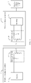
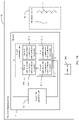
- FIG. 1 is a schematic diagram of a system architecture according to an embodiment of this application.
- the system architecture provided in this embodiment of this application may include but is not limited to a wireless charging transmitter 1, a wireless charging receiver 2, and an electric energy storage unit 3.
- the wireless charging transmitter 1 may include but is not limited to an inverter 11 and a resonant circuit 14 that includes a resonant capacitor 12 and a transmit coil 13.
- An output port of the inverter 11 is coupled to two ports of the resonant circuit 14.
- the foregoing inverter 11 is configured to perform inversion processing on an input electrical signal.
- the resonant circuit 14 is configured to: convert, into an electromagnetic signal, the electrical signal obtained after the inverter 11 performs inversion processing, and transmit the electromagnetic signal. Implementations of the inverter 11 and the wireless charging transmitter 1 are described in the following embodiments of this application.
- the wireless charging transmitter 1 may adjust an output voltage of the wireless charging transmitter 1 by switching an inversion mode of the inverter 11, to meet a required voltage coupled to a receive coil of a receive end.
- the wireless charging receiver 2 may include but is not limited to a rectifier 21 and a resonant circuit 24 that includes a resonant capacitor 22 and a receive coil 23.
- An input port of the rectifier 21 is coupled to an output port of the resonant circuit 24, and an output port of the rectifier 21 is coupled to the electric energy storage unit 3.
- the resonant circuit 24 is configured to convert, into an electrical signal, the electromagnetic signal received from the transmit coil 13.
- the rectifier 21 is configured to: perform rectification processing on the electrical signal output by the resonant circuit 24, and store, into the electric energy storage unit 3, electric energy obtained through processing. Implementations of the rectifier 21 and the wireless charging receiver 2 are described in the following embodiments of this application.
- the wireless charging receiver 2 may adjust an output voltage of the wireless charging receiver 2 by switching a rectification mode of the rectifier 21, to meet a power supply requirement.
- a unidirectional conduction semiconductor transistor in the embodiments of this application may be a metal-oxide semiconductor field-effect transistor (Metal-Oxide-Semiconductor Field-Effect Transistor, MOSFET) (or briefly referred to as a MOS transistor) or a diode.
- MOSFET Metal-Oxide-Semiconductor Field-Effect Transistor
- the unidirectional conduction semiconductor transistor may be another semiconductor transistor that has a unidirectional conduction function.
- Any MOS transistor in the embodiments of this application does not include only one MOS transistor.
- a plurality of MOS transistors may be connected in parallel to implement a low on-resistance, or a plurality of MOS transistors may be connected in series to implement a high withstand voltage.
- Any diode in the embodiments of this application does not include only one diode.
- a plurality of diodes may be connected in parallel to implement a low on-resistance, or a plurality of diodes may be connected in series to implement a high withstand voltage. This is not limited in the embodiments of this application.
- any unidirectional conduction semiconductor transistor is a diode
- an input port of the diode may be an anode of the diode
- an output port of the diode may be a cathode of the diode.
- Any switch in the embodiments of this application may be a MOS transistor or a mechanical switch.
- the switch may be another component that has a switch function. This is not limited in the embodiments of this application.
- the MOS transistor in the embodiments of this application may include a PMOS transistor or an NMOS transistor.
- An electronic device in the embodiments of this application may include but is not limited to a terminal device such as a mobile phone, a tablet computer, or a notebook computer.
- a wireless charging transmitter in the embodiments of this application may include but is not limited to a device that externally transmits a power, for example, a charging pad.
- a wireless charging receiver in the embodiments of this application may include but is not limited to a device that can receive a wireless charging power, for example, an electronic device with a battery, a medical device, or an electric vehicle.
- a wireless charging device in the embodiments of this application may include but is not limited to a wireless charging transmitter or a wireless charging receiver.
- a related technology has a technical problem that an output voltage of a rectifier circuit in a wireless charging receiver or an inverter circuit in a wireless charging transmitter is approximately equal to an input voltage of the rectifier circuit in the wireless charging receiver or the inverter circuit in the wireless charging transmitter.
- the rectifier or the inverter includes a signal conversion unit and a switchable capacitor unit that are coupled to each other.
- the switchable capacitor unit in the rectifier is configured to switch a rectification mode of the rectifier, or the switchable capacitor unit in the inverter is configured to switch an inversion mode of the inverter. Therefore, a variable dynamic range of an output voltage of the rectifier or the inverter provided in the embodiments of this application is large.
- FIG. 2A is a schematic diagram 1 of a structure of a conversion circuit according to an embodiment of this application.
- a conversion circuit 20 provided in this embodiment of this application may include a signal conversion unit 201 and a switchable capacitor unit 202.
- the conversion circuit 20 provided in this embodiment of this application may be a rectifier or an inverter.
- the signal conversion unit 201 may include but is not limited to: a first port a, a second port b, a third port c, a fourth port d, a first unidirectional conduction semiconductor transistor 2011, a second unidirectional conduction semiconductor transistor 2012, a third unidirectional conduction semiconductor transistor 2013, and a fourth unidirectional conduction semiconductor transistor 2014.
- a connection relationship of the signal conversion unit 201 may be as follows: An output port of the first unidirectional conduction semiconductor transistor 2011 and an input port of the second unidirectional conduction semiconductor transistor 2012 are coupled to the first port a. An output port of the second unidirectional conduction semiconductor transistor 2012 and an output port of the third unidirectional conduction semiconductor transistor 2013 are coupled to the second port b. An output port of the fourth unidirectional conduction semiconductor transistor 2014 and an input port of the third unidirectional conduction semiconductor transistor 2013 are coupled to the third port c. An input port of the first unidirectional conduction semiconductor transistor 2011 and an input port of the fourth unidirectional conduction semiconductor transistor 2014 are coupled to the fourth port d.
- the fourth port d is configured to be coupled to a constant voltage.
- the constant voltage may be a ground voltage.
- the first port a and the third port c are input ports of the rectifier, and are configured to be coupled to an output port of a resonant circuit 24.
- the second port b and the fourth port d are output ports of the rectifier, and are configured to be coupled to an electric energy storage unit 3.
- the first unidirectional conduction semiconductor transistor 2011, the second unidirectional conduction semiconductor transistor 2012, the third unidirectional conduction semiconductor transistor 2013, and the fourth unidirectional conduction semiconductor transistor 2014 may all be diodes.
- an input port of each diode may be an anode of the diode
- an output port of each diode may be a cathode of the diode.
- FIG. 2B is a schematic diagram 2 of a structure of a conversion circuit according to an embodiment of this application.
- the first unidirectional conduction semiconductor transistor 2011, the second unidirectional conduction semiconductor transistor 2012, the third unidirectional conduction semiconductor transistor 2013, and the fourth unidirectional conduction semiconductor transistor 2014 in this embodiment of this application may all be diodes.
- the first unidirectional conduction semiconductor transistor 2011, the second unidirectional conduction semiconductor transistor 2012, the third unidirectional conduction semiconductor transistor 2013, and the fourth unidirectional conduction semiconductor transistor 2014 may all be metal-oxide semiconductor MOS transistors.
- a connection direction of each MOS transistor needs to meet the following: An anode of a body diode of the MOS transistor is used as an input port of the MOS transistor, and a cathode of the body diode of the MOS transistor is used as an output port of the MOS transistor.
- any unidirectional conduction semiconductor transistor is a PMOS transistor
- an input port of the unidirectional conduction semiconductor transistor is a drain of the PMOS transistor
- an output port of the unidirectional conduction semiconductor transistor is a source of the PMOS transistor.
- an input port of the unidirectional conduction semiconductor transistor is a source of the NMOS transistor
- an output port of the unidirectional conduction semiconductor transistor is a drain of the NMOS transistor.
- the first unidirectional conduction semiconductor transistor 2011, the second unidirectional conduction semiconductor transistor 2012, the third unidirectional conduction semiconductor transistor 2013, and the fourth unidirectional conduction semiconductor transistor 2014 may all be PMOS transistors or NMOS transistors.
- FIG. 2C is a schematic diagram 3 of a structure of a conversion circuit according to an embodiment of this application.
- the first unidirectional conduction semiconductor transistor 2011, the second unidirectional conduction semiconductor transistor 2012, the third unidirectional conduction semiconductor transistor 2013, and the fourth unidirectional conduction semiconductor transistor 2014 in this embodiment of this application may all be NMOS transistors.
- an input port of each NMOS transistor may be a source of the NMOS transistor
- an output port of each NMOS transistor may be a drain of the NMOS transistor.
- some unidirectional conduction semiconductor transistors in the first unidirectional conduction semiconductor transistor 2011, the second unidirectional conduction semiconductor transistor 2012, the third unidirectional conduction semiconductor transistor 2013, and the fourth unidirectional conduction semiconductor transistor 2014 may be PMOS transistors, and some other unidirectional conduction semiconductor transistors may be NMOS transistors.
- a connection manner in this implementation needs to meet the following connection rule: (1) When the PMOS transistor is coupled to the NMOS transistor, a source of the PMOS transistor is coupled to a source of the NMOS transistor, or a drain of the PMOS transistor is coupled to a drain of the NMOS transistor. (2) A port configured to be coupled to the second port is the source of the PMOS transistor or the drain of the NMOS transistor.
- some unidirectional conduction semiconductor transistors in the first unidirectional conduction semiconductor transistor 2011, the second unidirectional conduction semiconductor transistor 2012, the third unidirectional conduction semiconductor transistor 2013, and the fourth unidirectional conduction semiconductor transistor 2014 may be diodes, and some other unidirectional conduction semiconductor transistors may be MOS transistors.
- An input port of each diode may be an anode of the diode, and an output port of each diode may be a cathode of the diode.
- a connection direction of each MOS transistor needs to meet the following: An anode of a body diode of the MOS transistor is used as an input port of the MOS transistor, and a cathode of the body diode of the MOS transistor is used as an output port of the MOS transistor.
- an input port of the unidirectional conduction semiconductor transistor is a drain of the PMOS transistor, and an output port of the unidirectional conduction semiconductor transistor is a source of the PMOS transistor.
- any unidirectional conduction semiconductor transistor is an NMOS transistor
- an input port of the unidirectional conduction semiconductor transistor is a source of the NMOS transistor
- an output port of the unidirectional conduction semiconductor transistor is a drain of the NMOS transistor.
- a gate of each MOS transistor in this embodiment of this application may be used as a control pin to receive a control signal to control the MOS transistor to be turned on or turned off.
- the NMOS transistor 2012 is used as an example.
- the control signal received by the gate of the NMOS transistor 2012 is used to control the NMOS transistor to be turned on, so that a current flows from the input port a of the NMOS transistor 2012 to the output port b.
- the control signal is used to control the NMOS transistor to be turned off, to prevent a current from reversely flowing from the output port b of the NMOS transistor 2012 to the input port a.
- the switchable capacitor unit 202 may be coupled to at least one of the first port a and the third port c, the second port b, and the fourth port d. It should be noted that for ease of drawing, the accompanying drawings in embodiments of this application are shown by using an example in which the switchable capacitor unit 202 is coupled to the third port c, the second port b, and the fourth port d. A person skilled in the art should understand that the switchable capacitor unit 202 may alternatively be coupled to the first port a, the second port b, and the fourth port d.
- the switchable capacitor unit 202 in this embodiment of this application is configured to switch a rectification mode of the conversion circuit 20 (namely, the rectifier).
- the rectification mode may include but is not limited to a voltage multiplier rectification mode and a full-bridge rectification mode.
- an output voltage of an output port of the conversion circuit 20 may be n times an input voltage of an input port of the conversion circuit 20, where n is a real number greater than 0.
- a difference between an output voltage of an output port of the conversion circuit 20 and an input voltage of an input port of the conversion circuit 20 may be equal to on-voltage drops of two unidirectional conduction semiconductor transistors in the signal conversion unit 201. Because the on-voltage drop of the unidirectional conduction semiconductor transistor is small, in this mode, it may be considered that the output voltage of the output port of the conversion circuit 20 is equal to the input voltage of the input port of the conversion circuit 20.
- the rectifier provided in embodiments of this application includes the signal conversion unit 201 and the switchable capacitor unit 202 that are mutually coupled.
- the switchable capacitor unit 202 is configured to switch the rectification mode of the rectifier. Therefore, a variable dynamic range of the output voltage of the rectifier provided in embodiments of this application is large.
- a connection relationship of the signal conversion unit 201 may be as follows: An input port of the first unidirectional conduction semiconductor transistor 2011 and an output port of the second unidirectional conduction semiconductor transistor 2012 are coupled to the first port a. An input port of the second unidirectional conduction semiconductor transistor 2012 and an input port of the third unidirectional conduction semiconductor transistor 2013 are coupled to the second port b. An input port of the fourth unidirectional conduction semiconductor transistor 2014 and an output port of the third unidirectional conduction semiconductor transistor 2013 are coupled to the third port c. An output port of the first unidirectional conduction semiconductor transistor 2011 and an output port of the fourth unidirectional conduction semiconductor transistor 2014 are coupled to the fourth port d.
- the fourth port d is configured to be coupled to a constant voltage.
- the constant voltage may be a ground voltage.
- the second port b and the fourth port d are input ports of the inverter.
- the first port a and the third port c are output ports of the inverter, and are configured to be coupled to two ports of the resonant circuit 14.
- the first unidirectional conduction semiconductor transistor 2011, the second unidirectional conduction semiconductor transistor 2012, the third unidirectional conduction semiconductor transistor 2013, and the fourth unidirectional conduction semiconductor transistor 2014 may all be metal-oxide semiconductor MOS transistors.
- a connection direction of each MOS transistor needs to meet the following: A cathode of a body diode of the MOS transistor is used as an input port of the MOS transistor, and an anode of the body diode of the MOS transistor is used as an output port of the MOS transistor.
- any unidirectional conduction semiconductor transistor is a PMOS transistor
- an input port of the unidirectional conduction semiconductor transistor is a source of the PMOS transistor
- an output port of the unidirectional conduction semiconductor transistor is a drain of the PMOS transistor.
- an input port of the unidirectional conduction semiconductor transistor is a drain of the NMOS transistor
- an output port of the unidirectional conduction semiconductor transistor is a source of the NMOS transistor.
- the first unidirectional conduction semiconductor transistor 2011, the second unidirectional conduction semiconductor transistor 2012, the third unidirectional conduction semiconductor transistor 2013, and the fourth unidirectional conduction semiconductor transistor 2014 may all be PMOS transistors or NMOS transistors as shown in FIG. 2C .
- an input port of each NMOS transistor may be a drain of the NMOS transistor
- an output port of each NMOS transistor may be a source of the NMOS transistor.
- some unidirectional conduction semiconductor transistors in the first unidirectional conduction semiconductor transistor 2011, the second unidirectional conduction semiconductor transistor 2012, the third unidirectional conduction semiconductor transistor 2013, and the fourth unidirectional conduction semiconductor transistor 2014 may be PMOS transistors, and some other unidirectional conduction semiconductor transistors may be NMOS transistors.
- a connection manner in this example needs to meet the following connection rule: (1) When the PMOS transistor is coupled to the NMOS transistor, a source of the PMOS transistor is coupled to a source of the NMOS transistor, or a drain of the PMOS transistor is coupled to a drain of the NMOS transistor. (2) A port configured to be coupled to the second port is the source of the PMOS transistor or the drain of the NMOS transistor.
- a gate of each MOS transistor in this embodiment of this application may be used as a control pin to receive a control signal to control the MOS transistor to be turned on or turned off, so as to control a current to pass the output port of the MOS transistor.
- a current may be prevented from flowing through the MOS transistor. This implements unidirectional conduction.
- the NMOS transistor 2012 is used as an example.
- the control signal received by the gate of the NMOS transistor 2012 is used to control the NMOS transistor to be turned on, so that a current flows from the input port b of the NMOS transistor 2012 to the output port a.
- the control signal is used to control the NMOS transistor to be turned off, to prevent a current from reversely flowing from the output port a of the NMOS transistor 2012 to the input port b.
- the switchable capacitor unit 202 may be coupled to at least one of the first port a and the third port c, the second port b, and the fourth port d. It should be noted that for ease of drawing, the accompanying drawings in embodiments of this application are shown by using an example in which the switchable capacitor unit 202 is coupled to the third port c, the second port b, and the fourth port d. A person skilled in the art should understand that the switchable capacitor unit 202 may alternatively be coupled to the first port a, the second port b, and the fourth port d.
- the switchable capacitor unit 202 in this embodiment of this application is configured to switch an inversion mode of the conversion circuit 20 (namely, the inverter).
- the inversion mode may include but is not limited to a voltage division inversion mode and a full-bridge inversion mode.
- a difference between an output voltage of an output port of the conversion circuit 20 and an input voltage of an input port of the conversion circuit 20 may be equal to on-voltage drops of two unidirectional conduction semiconductor transistors in the signal conversion unit 201. Because the on-voltage drop of the unidirectional conduction semiconductor transistor is small, in this mode, it may be considered that the output voltage of the output port of the conversion circuit 20 is equal to the input voltage of the input port of the conversion circuit 20.
- the inverter provided in embodiments of this application includes the signal conversion unit 201 and the switchable capacitor unit 202 that are mutually coupled.
- the switchable capacitor unit 202 is configured to switch the inversion mode of the inverter. Therefore, a variable dynamic range of the output voltage of the inverter provided in embodiments of this application is large.
- FIG. 3A is a schematic diagram 4 of a structure of a conversion circuit according to an embodiment of this application. Based on any one of the foregoing embodiments shown in FIG. 2A to FIG. 2C , a possible implementation of the switchable capacitor unit 202 is described in this embodiment of this application.
- the switchable capacitor unit 202 may include but is not limited to a first switch 202A and a capacitor unit 202B.
- the first switch 202A is coupled between the third port c and an internal node e
- the capacitor unit 202B is coupled to the second port b, the fourth port d, and the internal node e.
- a conversion mode of the conversion circuit 20 may be switched by turning on or turning off the first switch 202A.
- the conversion circuit 20 is a rectifier and the first switch 202A is turned on, the conversion circuit 20 is in the voltage multiplier rectification mode; or if the first switch 202A is turned off, the conversion circuit 20 is in the full-bridge rectification mode.
- the conversion circuit 20 is an inverter and the first switch 202A is turned on, the conversion circuit 20 is in the voltage division inversion mode; or if the first switch 202A is turned off, the conversion circuit 20 is in the full-bridge inversion mode.
- the first switch 202A in this embodiment of this application may be a mechanical switch or a MOS transistor.
- the MOS transistor may be a PMOS transistor or an NMOS transistor.
- FIG. 3B is a schematic diagram 5 of a structure of a conversion circuit according to an embodiment of this application.
- a source s of the NMOS transistor 1 may be coupled to the third port c, and a drain d of the NMOS transistor 1 is coupled to the internal node e.
- a gate g of the NMOS transistor 1 is configured to receive a control signal to control the NMOS transistor 1 to be turned on or turned off.
- the source s of the NMOS transistor 1 may be coupled to the internal node e, and the drain d of the NMOS transistor 1 is coupled to the third port c (this manner is not shown in the figure).
- a source s of the PMOS transistor 1 may be coupled to the third port c, and a drain d of the PMOS transistor 1 is coupled to the internal node e.
- a gate g of the PMOS transistor 1 is configured to receive a control signal to control the PMOS transistor 1 to be turned on or turned off.
- the source s of the PMOS transistor 1 may be coupled to the internal node e, and the drain d of the PMOS transistor 1 is coupled to the third port c (this manner is not shown in the figure).
- FIG. 3C is a schematic diagram 6 of a structure of a conversion circuit according to an embodiment of this application.
- the first switch 202A includes an NMOS transistor 2 and an NMOS transistor 3
- a source s of the NMOS transistor 2 may be coupled to the third port c
- a drain d of the NMOS transistor 2 is coupled to a drain d of the NMOS transistor 3
- a source s of the NMOS transistor 3 is coupled to the internal node e.
- drain d of the NMOS transistor 2 may be coupled to the third port c, the source s of the NMOS transistor 2 is coupled to the source s of the NMOS transistor 3, and the drain d of the NMOS transistor 3 is coupled to the internal node e (this manner is not shown in the figure).
- gates g of the NMOS transistor 2 and the NMOS transistor 3 are configured to receive a control signal to control a corresponding NMOS transistor to be turned on or turned off.
- the NMOS transistor 2 and the NMOS transistor 3 are simultaneously turned on or turned off under control of the control signal, so that bidirectional anti-backflow can be implemented.
- the NMOS transistor 2 and the NMOS transistor 3 that are configured to implement bidirectional anti-backflow may be replaced with one MOS transistor.
- the first switch 202A may include a PMOS transistor 2 and a PMOS transistor 3.
- a source s of the PMOS transistor 2 may be coupled to the third port c, a drain d of the PMOS transistor 2 is coupled to a drain d of the PMOS transistor 3, and a source s of the PMOS transistor 3 is coupled to the internal node e (this manner is not shown in the figure).
- the drain d of the PMOS transistor 2 may be coupled to the third port c
- the source s of the PMOS transistor 2 is coupled to the source s of the PMOS transistor 3, and the drain d of the PMOS transistor 3 is coupled to the internal node e (this manner is not shown in the figure).
- the first switch 202A may include one PMOS transistor and one NMOS transistor.
- a drain of the PMOS transistor may be coupled to the third port c, a source of the PMOS transistor is coupled to a drain of the NMOS transistor, and a source of the NMOS transistor may be coupled to the internal node e (this manner is not shown in the figure).
- a source of the PMOS transistor may be coupled to the third port c, a drain of the PMOS transistor is coupled to a source of the NMOS transistor, and a drain of the NMOS transistor may be coupled to the internal node e (this manner is not shown in the figure).
- the first switch 202A may be another component that has a switch function. This is not limited in this embodiment of this application.
- FIG. 3D is a schematic diagram 7 of a structure of a conversion circuit according to an embodiment of this application.
- the capacitor unit 202B may include but is not limited to a first capacitor C1 and a second capacitor C2.
- the first capacitor C1 may be coupled between the internal node e and the second port b
- the second capacitor C2 is coupled between the internal node e and the fourth port d.
- the conversion circuit 20 is a rectifier and the first switch 202A is turned on, the first unidirectional conduction semiconductor transistor 2011 and the second unidirectional conduction semiconductor transistor 2012 in the signal conversion unit 201 and the capacitor unit 202B are located in a voltage multiplier rectifier circuit.
- the first switch 202A is turned off, the first unidirectional conduction semiconductor transistor 2011, the second unidirectional conduction semiconductor transistor 2012, the third unidirectional conduction semiconductor transistor 2013, and the fourth unidirectional conduction semiconductor transistor 2014 in the signal conversion unit 201 and the capacitor unit 202B are located in a full-bridge rectifier circuit.
- the conversion circuit 20 is in the voltage multiplier rectification mode.
- the conversion circuit 20 is in the full-bridge rectification mode.
- the conversion circuit 20 is an inverter and the first switch 202A is turned on, the first unidirectional conduction semiconductor transistor 2011 and the second unidirectional conduction semiconductor transistor 2012 in the signal conversion unit 201 and the capacitor unit 202B are located in a voltage division inverter circuit.
- the first switch 202A is turned off, the first unidirectional conduction semiconductor transistor 2011, the second unidirectional conduction semiconductor transistor 2012, the third unidirectional conduction semiconductor transistor 2013, and the fourth unidirectional conduction semiconductor transistor 2014 in the signal conversion unit 201 and the capacitor unit 202B are located in a full-bridge inverter circuit.
- the conversion circuit 20 is in the voltage division inversion mode.
- the conversion circuit 20 is in the full-bridge inversion mode.
- FIG. 3E is a schematic diagram 8 of a structure of a conversion circuit according to an embodiment of this application.
- the capacitor unit 202B further includes a third capacitor C3.
- the third capacitor C3 is coupled between the second port b and the fourth port d.
- the first capacitor C1, the second capacitor C2, and the third capacitor C3 in the foregoing embodiment of this application may be configured to store energy.
- FIG. 3F is a schematic diagram 9 of a structure of a conversion circuit according to an embodiment of this application.
- the capacitor unit 202B may include but is not limited to a first capacitor C1 and a second capacitor C2.
- the first capacitor C1 may be coupled between the internal node e and a preset position
- the second capacitor C2 is coupled between the second port b and the fourth port d.
- the preset position may include any one of the following: the second port b, the fourth port d, or a preset voltage.
- the preset voltage may be a preset direct current power supply or a ground voltage.
- the conversion circuit 20 is a rectifier and the first switch 202A is turned on, the first unidirectional conduction semiconductor transistor 2011 and the second unidirectional conduction semiconductor transistor 2012 in the signal conversion unit 201 and the capacitor unit 202B are located in a voltage multiplier rectifier circuit.
- the first switch 202A is turned off, the first unidirectional conduction semiconductor transistor 2011, the second unidirectional conduction semiconductor transistor 2012, the third unidirectional conduction semiconductor transistor 2013, and the fourth unidirectional conduction semiconductor transistor 2014 in the signal conversion unit 201 and the capacitor unit 202B are located in a full-bridge rectifier circuit.
- the conversion circuit 20 is an inverter and the first switch 202A is turned on, the first unidirectional conduction semiconductor transistor 2011 and the second unidirectional conduction semiconductor transistor 2012 in the signal conversion unit 201 and the capacitor unit 202B are located in a voltage division inverter circuit.
- the first switch 202A is turned off, the first unidirectional conduction semiconductor transistor 2011, the second unidirectional conduction semiconductor transistor 2012, the third unidirectional conduction semiconductor transistor 2013, and the fourth unidirectional conduction semiconductor transistor 2014 in the signal conversion unit 201 and the capacitor unit 202B are located in a full-bridge inverter circuit.
- FIG. 4A is a schematic diagram 10 of a structure of a conversion circuit according to an embodiment of this application. Based on any one of the embodiments shown in FIG. 2A to FIG. 2C , another possible implementation of the switchable capacitor unit 202 is described in this embodiment of this application.
- the switchable capacitor unit 202 may include but is not limited to a first switch 202A, a first capacitor C1, and a second capacitor C2.
- the first capacitor C1 may be coupled between the third port c and an internal node e
- the first switch 202A is coupled between the internal node e and a preset position
- the second capacitor C2 is coupled between the second port b and the fourth port d.
- a conversion mode of the conversion circuit 20 may be switched by turning on or turning off the first switch 202A.
- the conversion circuit 20 is a rectifier and the first switch 202A is turned on, the conversion circuit 20 is in the voltage multiplier rectification mode; or if the first switch 202A is turned off, the conversion circuit 20 is in the full-bridge rectification mode.
- the conversion circuit 20 is an inverter and the first switch 202A is turned on, the conversion circuit 20 is in the voltage division inversion mode; or if the first switch 202A is turned off, the conversion circuit 20 is in the full-bridge inversion mode.
- the preset position may include any one of the following: the second port b, the fourth port d, or a preset voltage.
- the preset voltage may be a preset direct current power supply or a ground voltage.
- FIG. 4B is a schematic diagram 11 of a structure of a conversion circuit according to an embodiment of this application. As shown in FIG. 4B , based on the embodiment shown in FIG. 4A , the first switch 202A may be coupled between the internal node e and the second port b.
- FIG. 4C is a schematic diagram 12 of a structure of a conversion circuit according to an embodiment of this application. As shown in FIG. 4C , based on the embodiment shown in FIG. 4A , the first switch 202A may be coupled between the internal node e and the fourth port d.
- the conversion circuit 20 is a rectifier and the first switch 202A is turned on, the first unidirectional conduction semiconductor transistor 2011 and the second unidirectional conduction semiconductor transistor 2012 in the signal conversion unit 201, the first capacitor C1, and the second capacitor C2 are located in a voltage multiplier rectifier circuit.
- the first switch 202A is turned off, the first unidirectional conduction semiconductor transistor 2011, the second unidirectional conduction semiconductor transistor 2012, the third unidirectional conduction semiconductor transistor 2013, and the fourth unidirectional conduction semiconductor transistor 2014 in the signal conversion unit 201 and the second capacitor C2 are located in a full-bridge rectifier circuit.
- the conversion circuit 20 is in the voltage multiplier rectification mode.
- the conversion circuit 20 is in the full-bridge rectification mode.
- the conversion circuit 20 is an inverter and the first switch 202A is turned on, the first unidirectional conduction semiconductor transistor 2011 and the second unidirectional conduction semiconductor transistor 2012 in the signal conversion unit 201, the first capacitor C1, and the second capacitor C2 are located in a voltage division inverter circuit.
- the first switch 202A is turned off, the first unidirectional conduction semiconductor transistor 2011, the second unidirectional conduction semiconductor transistor 2012, the third unidirectional conduction semiconductor transistor 2013, and the fourth unidirectional conduction semiconductor transistor 2014 in the signal conversion unit 201 and the second capacitor C2 are located in a full-bridge inverter circuit.
- the conversion circuit 20 is in the voltage division inversion mode.
- the conversion circuit 20 is in the full-bridge inversion mode.
- the first switch 202A in this embodiment of this application may be a mechanical switch or a MOS transistor, and the MOS transistor may be a PMOS transistor or an NMOS transistor.
- FIG. 4D is a schematic diagram 13 of a structure of a conversion circuit according to an embodiment of this application. As shown in FIG. 4D , based on any one of the embodiments shown in FIG. 4A to FIG. 4C , when the first switch 202A is an NMOS transistor 1, a source s of the NMOS transistor 1 may be coupled to the internal node e, and a drain d of the NMOS transistor 1 is coupled to the preset position.
- a gate g of the NMOS transistor 1 is configured to receive a control signal to control the NMOS transistor 1 to be turned on or turned off. It should be understood that the source s of the NMOS transistor 1 may be coupled to the preset position, and the drain d of the NMOS transistor 1 is coupled to the internal node e (this manner is not shown in the figure).
- a source s of the PMOS transistor 1 may be coupled to the internal node e, and a drain d of the PMOS transistor 1 is coupled to the preset position.
- a gate g of the PMOS transistor 1 is configured to receive a control signal to control the NMOS transistor 1 to be turned on or turned off.
- the source s of the PMOS transistor 1 may be coupled to the preset position, and the drain d of the PMOS transistor 1 is coupled to the internal node e (this manner is not shown in the figure).
- FIG. 4E is a schematic diagram 14 of a structure of a conversion circuit according to an embodiment of this application.
- the first switch 202A includes an NMOS transistor 2 and an NMOS transistor 3
- a source s of the NMOS transistor 2 may be coupled to the internal node e
- a drain d of the NMOS transistor 2 is coupled to a drain d of the NMOS transistor 3
- a source s of the NMOS transistor 3 is coupled to the preset position.
- the drain d of the NMOS transistor 2 may be coupled to the internal node e, the source s of the NMOS transistor 2 is coupled to the source s of the NMOS transistor 3, and the drain d of the NMOS transistor 3 is coupled to the preset position (this manner is not shown in the figure).
- gates g of the NMOS transistor 2 and the NMOS transistor 3 are configured to receive a control signal to control a corresponding NMOS transistor to be turned on or turned off.
- the NMOS transistor 2 and the NMOS transistor 3 are simultaneously turned on or turned off under control of the control signal, so that bidirectional anti-backflow can be implemented.
- the NMOS transistor 2 and the NMOS transistor 3 that are configured to implement bidirectional anti-backflow may be replaced with one MOS transistor.
- the first switch 202A may include a PMOS transistor 2 and a PMOS transistor 3.
- a source s of the PNMOS transistor 2 may be coupled to the internal node e, a drain d of the PMOS transistor 2 is coupled to a drain d of the PMOS transistor 3, and a source s of the PMOS transistor 3 is coupled to the preset position.
- the drain d of the PMOS transistor 2 may be coupled to the internal node e
- the source s of the PMOS transistor 2 is coupled to the source s of the PMOS transistor 3
- the drain d of the PMOS transistor 3 is coupled to the preset position (this manner is not shown in the figure).
- the first switch 202A may include one PMOS transistor and one NMOS transistor.
- a drain of the PMOS transistor may be coupled to the internal node e, a source of the PMOS transistor is coupled to a drain of the NMOS transistor, and a source of the NMOS transistor may be coupled to the preset position (this manner is not shown in the figure).
- a source of the PMOS transistor may be coupled to the internal node e, a drain of the PMOS transistor is coupled to a source of the NMOS transistor, and a drain of the NMOS transistor may be coupled to the preset position (this manner is not shown in the figure).
- the first switch 202A may be another component that has a switch function. This is not limited in this embodiment of this application.
- the switchable capacitor unit 202 may further include a first switching unit and a second switching unit.
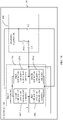
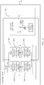
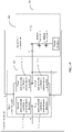
- FIG. 5 is a schematic diagram 15 of a structure of a conversion circuit according to an embodiment of this application.
- the switchable capacitor unit 202 may further include a first switching unit 202C and a second switching unit 202D.
- the first switching unit 202C is coupled between the internal node e and the first port a
- one port of the second switching unit 202D may be coupled to the fourth port d
- the other port of the second switching unit 202D may be coupled to a connection point (not shown in the figure) between a coil and a resonant capacitor in a resonant circuit.
- the conversion circuit 20 is an inverter and is disposed in the wireless charging transmitter 1
- the other port of the second switching unit 202D may be coupled to a connection point between the transmit coil 13 and the resonant capacitor 12 in the resonant circuit 14.
- the conversion circuit 20 is a rectifier and is disposed in the wireless charging receiver 2
- the other port of the second switching unit 202D may be coupled to a connection point between the receive coil 23 and the resonant capacitor in the resonant circuit 24.
- the first switching unit 202C may include but is not limited to a fifth unidirectional conduction semiconductor transistor 202C1 and a second switch 202C2.
- the second switch 202C2 may be coupled between the internal node e and an input port of the fifth unidirectional conduction semiconductor transistor 202C1, and an output port of the fifth unidirectional conduction semiconductor transistor 202C1 is coupled to the first port a. It should be understood that positions of the second switch 202C2 and the fifth unidirectional conduction semiconductor transistor 202C1 may be interchanged.
- the input port of the fifth unidirectional conduction semiconductor transistor 202C1 is coupled to the internal node e, and the second switch 202C2 is coupled between the first port a and the output port of the fifth unidirectional conduction semiconductor transistor 202C1 (this manner is not shown in the figure).
- the second switch 202C2 in this embodiment of this application may be a mechanical switch or a MOS transistor, and the MOS transistor may be a PMOS transistor or an NMOS transistor.
- the second switch 202C2 is a MOS transistor, a source and a drain of the MOS transistor are used as two ports of the second switch 202C2 to be respectively coupled to the internal node e and the input port of the fifth unidirectional conduction semiconductor transistor 202C1.
- the fifth unidirectional conduction semiconductor transistor 202C1 in this embodiment of this application may be a diode or a MOS transistor, and the MOS transistor may be a PMOS transistor or an NMOS transistor.
- the input port of the fifth unidirectional conduction semiconductor transistor 202C1 may be an anode of the diode
- the output port of the fifth unidirectional conduction semiconductor transistor 202C1 may be a cathode of the diode.
- the input port of the fifth unidirectional conduction semiconductor transistor 202C1 may be a source of the MOS transistor, and the output port of the fifth unidirectional conduction semiconductor transistor 202C1 may be a drain of the MOS transistor.
- the input port of the fifth unidirectional conduction semiconductor transistor 202C1 may be a drain of the MOS transistor, and the output port of the fifth unidirectional conduction semiconductor transistor 202C1 may be a source of the MOS transistor.
- which electrode of the MOS transistor the input port and/or the output port of the fifth unidirectional conduction semiconductor transistor 202C1 are/is may be further determined based on a type of the second switch 202C2 and a connection relationship between the fifth unidirectional conduction semiconductor transistor 202C1 and the second switch 202C2.
- the second switch 202C2 is an NMOS transistor 4
- the fifth unidirectional conduction semiconductor transistor 202C1 is an NMOS transistor 5
- a source of the NMOS transistor 4 may be coupled to a source of the NMOS transistor 5, or a drain of the NMOS transistor 4 is coupled to a drain of the NMOS transistor 5.
- the second switch 202C2 is a PMOS transistor 4
- the fifth unidirectional conduction semiconductor transistor 202C1 is a PMOS transistor 5
- a source of the PMOS transistor 4 may be coupled to a source of the PMOS transistor 5, or a drain of the PMOS transistor 4 is coupled to a drain of the PMOS transistor 5.
- the fifth unidirectional conduction semiconductor transistor 202C1 is a MOS transistor
- a source of the MOS transistor may be coupled to the mechanical switch, or a drain of the MOS transistor is coupled to the mechanical switch.
- the fifth unidirectional conduction semiconductor transistor 202C1 is a PMOS transistor
- the second switch 202C2 is an NMOS transistor
- a source of the PMOS transistor may be coupled to a drain of the NMOS transistor, or a drain of the PMOS transistor is coupled to a source of the NMOS transistor.
- a gate of the fifth unidirectional conduction semiconductor transistor 202C1 is used as a control pin to receive a control signal to control the fifth unidirectional conduction semiconductor transistor 202C1 to be turned on or turned off, and prevent the fifth unidirectional conduction semiconductor transistor 202C1 from being reversely turned on.
- positions of the fifth unidirectional conduction semiconductor transistor 202C1 and the second switch 202C2 may be interchanged.
- the second switching unit 202D may include but is not limited to a sixth unidirectional conduction semiconductor transistor 202D1 and a third switch 202D2.
- the third switch 202D2 may be coupled between the fourth port d and an input port of the sixth unidirectional conduction semiconductor transistor 202D1, and an output port of the sixth unidirectional conduction semiconductor transistor 202D1 may be coupled to the connection point (not shown in the figure) between the coil and the resonant capacitor in the resonant circuit.
- the conversion circuit 20 is an inverter and is disposed in the wireless charging transmitter 1
- the output port of the sixth unidirectional conduction semiconductor transistor 202D1 may be coupled to the connection point between the transmit coil 13 and the resonant capacitor 12 in the resonant circuit 14.
- the conversion circuit 20 is a rectifier and is disposed in the wireless charging receiver 2
- the output port of the sixth unidirectional conduction semiconductor transistor 202D1 may be coupled to the connection point between the receive coil 23 and the resonant capacitor in the resonant circuit 24.
- positions of the third switch 202D2 and the sixth unidirectional conduction semiconductor transistor 202D1 may be interchanged.
- the input port of the sixth unidirectional conduction semiconductor transistor 202D1 is coupled to the fourth port d
- the third switch 202D2 is coupled to a connection point between the output port of the sixth unidirectional conduction semiconductor transistor 202D1 and the resonant circuit (this manner is not shown in the figure).
- the third switch 202D2 in this embodiment of this application may be a mechanical switch or a MOS transistor, and the MOS transistor may be a PMOS transistor or an NMOS transistor.
- the third switch 202D2 is a MOS transistor
- a source and a drain of the MOS transistor are used as two ports of the third switch 202D2 to be respectively coupled to the fourth port d and the input port of the sixth unidirectional conduction semiconductor transistor 202D1.
- the source and the drain of the MOS transistor may be used as two ports of the third switch 202D2 to be respectively coupled to the output port of the sixth unidirectional conduction semiconductor transistor 202D1 and the connection point between the coil and the resonant capacitor in the resonant circuit.
- the sixth unidirectional conduction semiconductor transistor 202D1 in this embodiment of this application may be a diode or a MOS transistor, and the MOS transistor may be a PMOS transistor or an NMOS transistor.
- the input port of the sixth unidirectional conduction semiconductor transistor 202D1 may be an anode of the diode
- the output port of the sixth unidirectional conduction semiconductor transistor 202D1 may be a cathode of the diode.
- the input port of the sixth unidirectional conduction semiconductor transistor 202D1 may be a source of the MOS transistor, and the output port of the sixth unidirectional conduction semiconductor transistor 202D1 may be a drain of the MOS transistor.
- the input port of the sixth unidirectional conduction semiconductor transistor 202D1 may be a drain of the MOS transistor, and the output port of the sixth unidirectional conduction semiconductor transistor 202D1 may be a source of the MOS transistor.
- which electrode of the MOS transistor the input port and/or the output port of the sixth unidirectional conduction semiconductor transistor 202D1 are/is may be determined based on a type of the third switch 202D2 and a connection relationship the sixth unidirectional conduction semiconductor transistor 202D1 and the third switch 202D2.
- the third switch 202D2 is an NMOS transistor 6
- the sixth unidirectional conduction semiconductor transistor 202D1 is an NMOS transistor 7
- a source of the NMOS transistor 6 may be coupled to a source of the NMOS transistor 7, or a drain of the NMOS transistor 6 is coupled to a drain of the NMOS transistor 7.
- the third switch 202D2 is a PMOS transistor 6, and the sixth unidirectional conduction semiconductor transistor 202D1 is a PMOS transistor 7, a source of the PMOS transistor 6 may be coupled to a source of the PMOS transistor 7, or a drain of the PMOS transistor 6 is coupled to a drain of the PMOS transistor 7.
- the third switch 202D2 is a mechanical switch
- the sixth unidirectional conduction semiconductor transistor 202D1 is a MOS transistor
- a source of the MOS transistor may be coupled to the mechanical switch, or a drain of the MOS transistor is coupled to the mechanical switch.
- the sixth unidirectional conduction semiconductor transistor 202D1 is a PMOS transistor
- the third switch 202D2 is an NMOS transistor
- a source of the PMOS transistor may be coupled to a drain of the NMOS transistor, or a drain of the PMOS transistor is coupled to a source of the NMOS transistor.
- a gate of the sixth unidirectional conduction semiconductor transistor 202D1 is used as a control pin to receive a control signal to control the sixth unidirectional conduction semiconductor transistor 202D1 to be turned on or turned off, and prevent the sixth unidirectional conduction semiconductor transistor 202D1 from being unintendedly turned on. It should be understood that positions of the sixth unidirectional conduction semiconductor transistor 202D1 and the third switch 202D2 may be interchanged.
- the conversion mode of the conversion circuit 20 may be switched by turning off or turning on the fifth unidirectional conduction semiconductor transistor 202C1 and the second switch 202C2 in the first switching unit 202C, and the sixth unidirectional conduction semiconductor transistor 202D1 and the third switch 202D2 in the second switching unit 202D in cooperation with turn-on or turn-off of the first switch 202A.
- the conversion circuit 20 is a rectifier
- the first switch 202A is turned on
- the fifth unidirectional conduction semiconductor transistor 202C1 and/or the second switch 202C2 in the first switching unit 202C are/is turned off
- the sixth unidirectional conduction semiconductor transistor 202D1 and/or the third switch 202D2 in the second switching unit 202D are/is turned off
- the conversion circuit 20 is in the n1 voltage multiplier rectification mode.
- n1 for example, 2 voltage multiplier rectification mode
- Output voltage twice the input voltage - on-voltage drop of the unidirectional conduction semiconductor transistor in the signal conversion unit 201 - on-voltage drop of the first switch 202A.
- the conversion circuit 20 is an inverter
- the first switch 202A is turned on
- the fifth unidirectional conduction semiconductor transistor 202C1 and/or the second switch 202C2 in the first switching unit 202C are/is turned off
- the sixth unidirectional conduction semiconductor transistor 202D1 and/or the third switch 202D2 in the second switching unit 202D are/is turned off
- the conversion circuit 20 is in the 1/n1 voltage division inversion mode.
- Input voltage twice the output voltage - on-voltage drop of the unidirectional conduction semiconductor transistor in the signal conversion unit 201 - on-voltage drop of the first switch 202A.
- the conversion circuit 20 is a rectifier, and the first switch 202A, the second switch 202C2 in the first switching unit 202C, and the third switch 202D2 in the second switching unit 202D are turned on, the conversion circuit 20 is in the n2 (for example, 3) voltage multiplier rectification mode.
- Output voltage three times of the input voltage - on-voltage drop of the unidirectional conduction semiconductor transistor in the signal conversion unit 201 - on-voltage drops of the fifth unidirectional conduction semiconductor transistor 202C1 and the second switch 202C2 in the first switching unit 202C - on-voltage drops of the sixth unidirectional conduction semiconductor transistor 202D1 and the third switch 202D2 in the second switching unit 202D.
- the conversion circuit 20 is an inverter, and the first switch 202A, the second switch 202C2 in the first switching unit 202C, and the third switch 202D2 in the second switching unit 202D are turned on, the conversion circuit 20 is in the 1/n2 voltage division inversion mode.
- Input voltage three times of the output voltage - on-voltage drop of the unidirectional conduction semiconductor transistor in the signal conversion unit 201 - on-voltage drops of the fifth unidirectional conduction semiconductor transistor 202C1 and the second switch 202C2 in the first switching unit 202C - on-voltage drops of the sixth unidirectional conduction semiconductor transistor 202D1 and the third switch 202D2 in the second switching unit 202D.
- the conversion circuit 20 is a rectifier
- the first switch 202A is turned off
- the fifth unidirectional conduction semiconductor transistor 202C1 and/or the second switch 202C2 in the first switching unit 202C are/is turned off
- the sixth unidirectional conduction semiconductor transistor 202D1 and/or the third switch 202D2 in the second switching unit 202D are/is turned off
- the conversion circuit 20 is in the full-bridge rectification mode.
- the conversion circuit 20 is an inverter
- the first switch 202A is turned off
- the fifth unidirectional conduction semiconductor transistor 202C1 and/or the second switch 202C2 in the first switching unit 202C are/is turned off
- the sixth unidirectional conduction semiconductor transistor 202D1 and/or the third switch 202D2 in the second switching unit 202D are/is turned off
- the conversion circuit 20 is in the full-bridge inversion mode.
- more conversion modes of the conversion circuit 20 may be switched by turning on or turning off the first switching unit 202C and the second switching unit 202D in cooperation with turn-on or turn-off of the first switch 202A.
- the conversion circuit 20 is a rectifier
- more rectification modes of the rectifier may be switched by turning on or turning off the first switching unit 202C and the second switching unit 202D in cooperation with turn-on or turn-off of the first switch 202A.
- the conversion circuit 20 is an inverter
- more inversion modes of the inverter may be switched by turning on or turning off the first switching unit 202C and the second switching unit 202D in cooperation with turn-on or turn-off of the first switch 202A. It may be learned that the variable dynamic range of the output voltage of the rectifier or the inverter provided in this embodiment of this application is further increased.
- FIG. 6A is a schematic diagram 16 of a structure of a conversion circuit according to an embodiment of this application.
- the conversion circuit 20 is a rectifier, because a voltage of an input port of the conversion circuit 20 is small in some cases, to avoid an impact on switching of the rectification mode of the conversion circuit 20, the conversion circuit 20 provided in this embodiment of this application may further include an assisted boost circuit.
- the conversion circuit 20 further includes an assisted boost circuit 203.
- the assisted boost circuit 203 may be coupled between the first port a and the second port b, and an output port O of the assisted boost circuit 203 may be configured to be coupled to a controller.
- the assisted boost circuit 203 is configured to perform voltage boost on a voltage of the first port a, so that a voltage obtained after voltage boost meets a startup voltage of the controller, and the controller can generate a switching signal used to control the switchable capacitor unit 202 and a control signal used to control each unidirectional conduction semiconductor transistor in the signal conversion unit 201, to switch the rectification mode of the conversion circuit 20.
- the controller can generate a switching signal used to control the switchable capacitor unit 202 and a control signal used to control each unidirectional conduction semiconductor transistor in the signal conversion unit 201, to switch the rectification mode of the conversion circuit 20.
- FIG. 6B is a schematic diagram 17 of a structure of a conversion circuit according to an embodiment of this application. Based on the embodiment shown in FIG. 6A , an implementation of the assisted boost circuit 203 is described in this embodiment of this application. As shown in FIG. 6B , the assisted boost circuit 203 may include but is not limited to a first diode D1, a second diode D2, a fourth capacitor C4, and a fifth capacitor C5.
- An input port of the first diode D1 is coupled to the second port b, an input port of the second diode D2 and a first port of the fourth capacitor C4 are coupled to an output port of the first diode D1, a second port of the fourth capacitor C4 is coupled to the first port a, an output port of the second diode D2 and a first port of the fifth capacitor C5 are coupled to the output port O, and a second port of the fifth capacitor C5 is grounded.
- One time period is used as an example.
- the assisted boost circuit 203 provided in this embodiment of this application, in the first half period, when the voltage of the first port a is less than a voltage of the third port c, the fourth capacitor C4 is charged by using the third unidirectional conduction semiconductor transistor 2013 and the first diode D1, so that a voltage of an upper end of the fourth capacitor C4 is approximately equal to a voltage between the first port a and the third port c.
- the fifth capacitor C5 is charged by using the fourth capacitor C4 and the second diode D2.
- a voltage of an upper end (namely, the output port O) of the fifth capacitor C5 is approximately equal to a sum of the voltage between the first port a and the third port c and a voltage of two ports of the fourth capacitor C4. It may be learned that the voltage of the output port O may be approximately twice the voltage of the first port a, so that the startup voltage of the controller can be met. For example, in a ping (or referred to as a protocol initial power-on) phase, with the assisted boost circuit 203, the voltage of the output port O may be increased, so that the startup voltage of the controller can be met, and a degree of freedom in the ping phase can be improved.
- the degree of freedom in this embodiment of this application is a placement location relationship between the wireless charging transmitter and the wireless charging receiver, including horizontal and spatial distances.
- the wireless charging device is configured to receive a wireless charging signal.
- the wireless charging device is the wireless charging receiver 2.
- the wireless charging receiver 2 may include but is not limited to the resonant circuit 24 and the rectifier 21.
- FIG. 7A is a schematic diagram 1 of a structure of a wireless charging device according to an embodiment of this application.
- a wireless charging device 70 provided in this embodiment of this application may include but is not limited to the resonant circuit 24, the rectifier 21, a controller 701, and a charging management unit 702.
- the controller 701 is coupled to the rectifier 21, and is configured to control the signal conversion unit 201 and the switchable capacitor unit 202 in the rectifier 21.
- the controller 701 may be connected to a gate of a unidirectional conduction semiconductor transistor in the signal conversion unit 201, and connected to a switch and a gate of a unidirectional conduction semiconductor transistor in the switchable capacitor unit 202.
- the first port a and the third port c of the rectifier 21 are used as input ports to be respectively coupled to two ports of the resonant circuit 24, and are configured to receive an electrical signal obtained by the resonant circuit 24 by converting an electromagnetic signal received from a transmit coil of a peer end.
- the second port b and the fourth port d of the rectifier 21 are output ports of the rectifier 21, and are configured to be coupled to the charging management unit 702 that is configured to perform voltage conversion (for example, voltage buck) on an output voltage of the output port of the rectifier 21, to match a storage voltage of a subsequent electric energy storage unit.
- the electric energy storage unit may include but is not limited to a battery. It should be noted that the electric energy storage unit may belong to the wireless charging device 70, or may belong to an electronic device connected to the wireless charging device 70.
- an inductance value of the receive coil 23 in the resonant circuit 24 in this embodiment of this application is less than an inductance value of a standard receive coil, so that a resistance of the receive coil can be reduced, heat consumption of the receive coil can be reduced, and a through-current capability of the receive coil can be improved.
- a wireless charging device that complies with the international wireless charging standard Qi protocol introduced by the Wireless Power Consortium (Wireless Power Consortium, WPC), a shape and a specification of a coil of a transmit end are specifically specified in the protocol.
- a requirement on a voltage to which the standard receive coil is coupled is as follows: In a ping phase, a voltage to which the standard receive coil is coupled needs to be greater than 2.7 V, so that a chip of the wireless charging device can be normally powered on. In an initial power transmission phase, the voltage to which the standard receive coil is coupled needs to be greater than 5 V, so that a cascade device can be charged.
- the inductance value of the receive coil in this embodiment of this application may be 1/(n ⁇ 2) of the inductance value of the standard receive coil.
- the controller 701 is configured to control the switchable capacitor unit 202 in the rectifier 21 to switch a rectification mode of the rectifier 21.
- the rectification mode includes a voltage multiplier rectification mode or a full-bridge rectification mode. It should be understood that the controller 701 is further configured to control each unidirectional conduction semiconductor transistor in the signal conversion unit 201 to be turned on or turned off.
- the controller 701 may switch the rectification mode of the rectifier 21 by controlling the unidirectional conduction semiconductor transistor and/or the switch in the switchable capacitor unit 202 to be turned on or turned off.
- the controller 701 is configured to control the switchable capacitor unit based on wireless charging running state information of the device 70, to switch the rectification mode of the rectifier 21.
- the controller 701 is configured to control the switchable capacitor unit based on a preset voltage threshold and the preset port voltage, to switch the rectification mode of the rectifier 21.
- the preset port voltage may include but is not limited to an input voltage of an input port of the rectifier 21 or an output voltage of an output port of the rectifier 21.
- the controller 701 is configured to control the unidirectional conduction semiconductor transistor and/or the switch in the switchable capacitor unit 202 to be turned on or turned off, so that the rectifier 21 is in the voltage multiplier rectification mode, and the output voltage of the output port of the rectifier 21 can be greater than the input voltage of the input port of the rectifier 21. Therefore, it can be ensured that the device 70 can supply power to the cascade device.
- the controller 701 is configured to control the unidirectional conduction semiconductor transistor and/or the switch in the switchable capacitor unit 202 to be turned on or turned off, so that the rectifier 21 is in the full-bridge rectification mode, and the output voltage of the output port of the rectifier 21 is almost equal to the input voltage of the input port of the rectifier 21.
- the controller 701 is configured to control the switchable capacitor unit based on the charging mode of the device 70, to switch the rectification mode of the conversion circuit 20.
- the charging mode of the device 70 may include but is not limited to an extended power profile (Extended Power Profile, EPP) mode, a baseline power profile (Baseline Power Profile, BPP) mode, or a private fast charging mode
- the controller 701 is configured to control the switchable capacitor unit based on the preset voltage threshold and the preset port voltage, to switch the rectification mode of the rectifier 21. Therefore, stability of an output voltage of the device can be ensured.
- the rectification mode of the rectifier 21 is switched, so that the output voltage of the device 70 can be adjusted, to meet a power supply requirement.
- the wireless charging device in this embodiment of this application is configured to send a wireless charging signal.
- the wireless charging device is the wireless charging transmitter 1.
- the wireless charging transmitter 1 may include but is not limited to the inverter 11 and the resonant circuit 14.
- FIG. 7B is a schematic diagram 2 of a structure of a wireless charging device according to an embodiment of this application.
- a wireless charging device 80 provided in this embodiment of this application may include but is not limited to the resonant circuit 14, the inverter 11, and a controller 801.
- the controller 801 is coupled to the inverter 11, and is configured to control the signal conversion unit 201 and the switchable capacitor unit 202 in the inverter 11.
- the controller 801 may be connected to a gate of a unidirectional conduction semiconductor transistor in the signal conversion unit 201, and connected to a switch and a gate of a unidirectional conduction semiconductor transistor in the switchable capacitor unit 202.
- the second port b and the fourth port d of the inverter 11 are input ports of the inverter 11.
- the first port a and the third port c of the inverter 11 are used as output ports to be respectively coupled to two ports of the resonant circuit 14, so that the resonant circuit 14 converts, into an electromagnetic signal, an electrical signal output by the inverter 11, and transmits the electromagnetic signal.
- the controller 801 is configured to control the switchable capacitor unit 202 in the inverter 11 to switch an inversion mode of the inverter 11.
- the inversion mode includes a voltage division inversion mode or a full-bridge inversion mode.
- the controller 801 is further configured to control each unidirectional conduction semiconductor transistor in the signal conversion unit 201 to be turned on or turned off.
- the controller 801 switches the inversion mode of the inverter 11 by controlling the unidirectional conduction semiconductor transistor and/or the switch in the switchable capacitor unit 202 to be turned on or turned off.
- the controller 801 is configured to control the switchable capacitor unit based on wireless charging running state information of the device 80, to switch the inversion mode of the inverter 11.
- the controller 801 is configured to control the switchable capacitor unit based on a preset voltage threshold and the preset port voltage, to switch the inversion mode of the inverter 11.
- the preset port voltage may include but is not limited to an input voltage of an input port of the inverter 11 or an output voltage of an output port of the inverter 11.
- the controller 801 is configured to control the unidirectional conduction semiconductor transistor and/or the switch in the switchable capacitor unit 202 to be turned on or turned off, so that the inverter 11 is in the voltage division inversion mode, and the output voltage of the output port of the inverter 11 can be less than the input voltage of the input port of the inverter 11. Therefore, it can be ensured that a receive coil of a receive end can be coupled to a voltage meeting a preset coupled voltage range.
- the controller 801 is configured to control the unidirectional conduction semiconductor transistor and/or the switch in the switchable capacitor unit 202 to be turned on or turned off, so that the inverter 11 is in the full-bridge inversion mode, and the output voltage of the output port of the inverter 11 is almost equal to the input voltage of the input port of the inverter 11. Therefore, it can be ensured as much as possible that a receive coil of a receive end can be coupled to a voltage meeting a preset coupled voltage range.
- the controller 801 controls the switchable capacitor unit based on wireless charging running state information of the device 80, to switch the inversion mode of the inverter 11.
- the inversion mode of the inverter 11 is switched, so that an output voltage of the device 80 can be adjusted, to meet a required voltage coupled to the receive coil of the receive end.
Landscapes
- Engineering & Computer Science (AREA)
- Power Engineering (AREA)
- Computer Networks & Wireless Communication (AREA)
- Manufacturing & Machinery (AREA)
- Chemical & Material Sciences (AREA)
- Chemical Kinetics & Catalysis (AREA)
- Electrochemistry (AREA)
- General Chemical & Material Sciences (AREA)
- Rectifiers (AREA)
- Charge And Discharge Circuits For Batteries Or The Like (AREA)
Abstract
Description
- This application relates to the field of wireless charging technologies, and in particular, to a rectifier, an inverter, and a wireless charging device.
- With the development of wireless charging technologies, the wireless charging technologies are increasingly applied to different electronic products. The wireless charging technology is a technology in which electric energy is transmitted between a charger and a power consumption device by using a magnetic field, and user equipment can be charged without connecting the charger and the power consumption device by using a wire.
- In a related technology, a wireless charging receiver generally includes a resonant circuit and a rectifier circuit. The resonant circuit is configured to convert an electromagnetic signal obtained from a wireless charging transmitter. The rectifier circuit is configured to rectify a signal output by the resonant circuit. In addition, the rectifier circuit runs in a full-bridge rectification mode, that is, an output voltage of an output port of the rectifier circuit is approximately equal to an input voltage of an input port of the rectifier circuit.
- Similarly, the wireless charging transmitter generally includes a resonant circuit and an inverter circuit. The resonant circuit is configured to convert, into an electromagnetic signal, a signal output by the inverter circuit. The inverter circuit is configured to perform inversion processing on an input signal, so that the resonant circuit transmits the electromagnetic signal. In addition, the inverter circuit runs in a full-bridge inversion mode, that is, an output voltage of an output port of the inverter circuit is approximately equal to an input voltage of an input port of the inverter circuit.
- It may be learned that, in the related technology, an output voltage of the rectifier circuit in the wireless charging receiver or the inverter circuit in the wireless charging transmitter is approximately equal to an input voltage of the rectifier circuit in the wireless charging receiver or the inverter circuit in the wireless charging transmitter, and has a small variable dynamic range.
- This application provides a rectifier, an inverter, and a wireless charging device, to resolve a technical problem, in a related technology, that a variable dynamic range of an output voltage of a rectifier circuit in a wireless charging receiver or an inverter circuit in a wireless charging transmitter is small.
- According to a first aspect, an embodiment of this application provides a rectifier, including a signal conversion unit and a switchable capacitor unit. The signal conversion unit includes a first port, a second port, a third port, a fourth port, a first unidirectional conduction semiconductor transistor, a second unidirectional conduction semiconductor transistor, a third unidirectional conduction semiconductor transistor, and a fourth unidirectional conduction semiconductor transistor. An output port of the first unidirectional conduction semiconductor transistor and an input port of the second unidirectional conduction semiconductor transistor are coupled to the first port. An output port of the second unidirectional conduction semiconductor transistor and an output port of the third unidirectional conduction semiconductor transistor are coupled to the second port. An output port of the fourth unidirectional conduction semiconductor transistor and an input port of the third unidirectional conduction semiconductor transistor are coupled to the third port. An input port of the first unidirectional conduction semiconductor transistor and an input port of the fourth unidirectional conduction semiconductor transistor are coupled to the fourth port. The first port and the third port are configured to be coupled to a resonant circuit. The fourth port is configured to be coupled to a constant voltage. The switchable capacitor unit is coupled to at least one of the first port and the third port, the second port, and the fourth port. The first port and the third port are input ports of the rectifier. The second port and the fourth port are output ports of the rectifier. The constant voltage may be a ground voltage.
- The switchable capacitor unit in this embodiment of this application is configured to switch a rectification mode of the rectifier. The rectification mode may include but is not limited to a voltage multiplier rectification mode and a full-bridge rectification mode.
- For example, the first unidirectional conduction semiconductor transistor, the second unidirectional conduction semiconductor transistor, the third unidirectional conduction semiconductor transistor, and the fourth unidirectional conduction semiconductor transistor may all be diodes. Correspondingly, an input port of each diode may be an anode of the diode, and an output port of each diode may be a cathode of the diode.
- For another example, the first unidirectional conduction semiconductor transistor, the second unidirectional conduction semiconductor transistor, the third unidirectional conduction semiconductor transistor, and the fourth unidirectional conduction semiconductor transistor may all be metal-oxide semiconductor MOS transistors. A connection direction of each MOS transistor needs to meet the following: An anode of a body diode of the MOS transistor is used as an input port of the MOS transistor, and a cathode of the body diode of the MOS transistor is used as an output port of the MOS transistor. For example, if any unidirectional conduction semiconductor transistor is a PMOS transistor, an input port of the unidirectional conduction semiconductor transistor is a drain of the PMOS transistor, and an output port of the unidirectional conduction semiconductor transistor is a source of the PMOS transistor. Alternatively, if any unidirectional conduction semiconductor transistor is an NMOS transistor, an input port of the unidirectional conduction semiconductor transistor is a source of the NMOS transistor, and an output port of the unidirectional conduction semiconductor transistor is a drain of the NMOS transistor.
- In an example, the first unidirectional conduction semiconductor transistor, the second unidirectional conduction semiconductor transistor, the third unidirectional conduction semiconductor transistor, and the fourth unidirectional conduction semiconductor transistor may all be PMOS transistors or NMOS transistors.
- In another example, some unidirectional conduction semiconductor transistors in the first unidirectional conduction semiconductor transistor, the second unidirectional conduction semiconductor transistor, the third unidirectional conduction semiconductor transistor, and the fourth unidirectional conduction semiconductor transistor may be PMOS transistors, and some other unidirectional conduction semiconductor transistors may be NMOS transistors. It should be noted that a connection manner in this example needs to meet the following connection rule: (1) When the PMOS transistor is coupled to the NMOS transistor, a source of the PMOS transistor is coupled to a source of the NMOS transistor, or a drain of the PMOS transistor is coupled to a drain of the NMOS transistor. (2) A port configured to be coupled to the second port is the source of the PMOS transistor or the drain of the NMOS transistor.
- For another example, some unidirectional conduction semiconductor transistors in the first unidirectional conduction semiconductor transistor, the second unidirectional conduction semiconductor transistor, the third unidirectional conduction semiconductor transistor, and the fourth unidirectional conduction semiconductor transistor may be diodes, and some other unidirectional conduction semiconductor transistors may be MOS transistors. An input port of each diode may be an anode of the diode, and an output port of each diode may be a cathode of the diode. A connection direction of each MOS transistor needs to meet the following: An anode of a body diode of the MOS transistor is used as an input port of the MOS transistor, and a cathode of the body diode of the MOS transistor is used as an output port of the MOS transistor. For example, if any unidirectional conduction semiconductor transistor is a PMOS transistor, an input port of the unidirectional conduction semiconductor transistor is a drain of the PMOS transistor, and an output port of the unidirectional conduction semiconductor transistor is a source of the PMOS transistor. Alternatively, if any unidirectional conduction semiconductor transistor is an NMOS transistor, an input port of the unidirectional conduction semiconductor transistor is a source of the NMOS transistor, and an output port of the unidirectional conduction semiconductor transistor is a drain of the NMOS transistor.
- In addition, a gate of each MOS transistor may be used as a control pin to receive a control signal to control the MOS transistor to be turned on or turned off, so as to control a current to pass the output port of the MOS transistor.
- The rectifier provided in this embodiment of this application includes the signal conversion unit and the switchable capacitor unit that are mutually coupled. The switchable capacitor unit is configured to switch the rectification mode of the rectifier. Therefore, a variable dynamic range of an output voltage of the rectifier provided in this embodiment of this application is large.
- In a possible implementation, the switchable capacitor unit includes a first switch and a capacitor unit, the first switch is coupled between the third port and an internal node, and the capacitor unit is coupled to the second port, the fourth port, and the internal node.
- In a possible implementation, the capacitor unit includes a first capacitor and a second capacitor, the first capacitor is coupled between the internal node and the second port, and the second capacitor is coupled between the internal node and the fourth port.
- In a possible implementation, the capacitor unit further includes a third capacitor, and the third capacitor is coupled between the second port and the fourth port.
- In a possible implementation, the capacitor unit includes a first capacitor and a second capacitor, the first capacitor is coupled between the internal node and a preset position, and the second capacitor is coupled between the second port and the fourth port. For example, the preset position includes any one of the following: the second port, the fourth port, or a preset voltage.
- In a possible implementation, the switchable capacitor unit includes a first switch, a first capacitor, and a second capacitor, the first capacitor is coupled between the third port and an internal node, the first switch is coupled between the internal node and a preset position, and the second capacitor is coupled between the second port and the fourth port. For example, the preset position includes any one of the following: the second port, the fourth port, or a preset voltage.
- In a possible implementation, the switchable capacitor unit further includes a first switching unit and a second switching unit, the first switching unit is coupled between the internal node and the first port, and the second switching unit is coupled between the fourth port and the resonant circuit.
- In this implementation, the rectification mode of the rectifier may be switched by turning on or turning off the first switching unit and the second switching unit in cooperation with turn-on or turn-off of the first switch.
- In a possible implementation, the first switching unit includes a fifth unidirectional conduction semiconductor transistor and a second switch. The second switch is coupled between the internal node and an input port of the fifth unidirectional conduction semiconductor transistor, and an output port of the fifth unidirectional conduction semiconductor transistor is coupled to the first port. Alternatively, an input port of the fifth unidirectional conduction semiconductor transistor is coupled to the internal node, and the second switch is coupled between the first port and an output port of the fifth unidirectional conduction semiconductor transistor.
- For example, the second switch may be a mechanical switch or a MOS transistor, and/or the fifth unidirectional conduction semiconductor transistor may be a diode or a MOS transistor. The MOS transistor may be a PMOS transistor or an NMOS transistor.
- In a possible implementation, the second switching unit includes a sixth unidirectional conduction semiconductor transistor and a third switch. The third switch is coupled between the fourth port and an input port of the sixth unidirectional conduction semiconductor transistor, and an output port of the sixth unidirectional conduction semiconductor transistor is coupled to the resonant circuit. Alternatively, an input port of the sixth unidirectional conduction semiconductor transistor is coupled to the fourth port, and the third switch is coupled between an output port of the sixth unidirectional conduction semiconductor transistor and the resonant circuit.
- For example, the third switch may be a mechanical switch or a MOS transistor, and/or the sixth unidirectional conduction semiconductor transistor may be a diode or a MOS transistor. The MOS transistor may be a PMOS transistor or an NMOS transistor.
- In an example, if the first switch is turned on, and both the first switching unit and the second switching unit are turned off, the rectifier is in an n1 voltage multiplier rectification mode, where n1 is a real number greater than 0.
- In another example, if the first switch, the second switch in the first switching unit, and the third switch in the second switching unit are turned on, the rectifier is in an n2 voltage multiplier rectification mode, where n2 is a real number greater than 0, and n2 is greater than n1.
- In another example, if the first switch, the first switching unit, and the second switching unit are all turned off, the rectifier is in the full-bridge rectification mode.
- According to the rectifier provided in this embodiment, more rectification modes of the rectifier may be switched by turning on or turning off the first switching unit and the second switching unit in cooperation with turn-on or turn-off of the first switch. It may be learned that the variable dynamic range of the output voltage of the rectifier provided in this embodiment of this application is further increased.
- In a possible implementation, the rectifier further includes an assisted boost circuit, and the assisted boost circuit is coupled between the first port and the second port, and is configured to perform voltage boost on a voltage of the first port, so that a voltage obtained after voltage boost meets a startup voltage of a controller, and the controller can control the switchable capacitor unit to switch the rectification mode of the rectifier.
- According to a second aspect, an embodiment of this application provides a wireless charging device, where the device is configured to receive a wireless charging signal, and the device includes the rectifier according to any one of the implementations of the first aspect and a resonant circuit.
- In a possible implementation, the device further includes a controller, configured to control a switchable capacitor unit to switch a rectification mode of the rectifier. The rectification mode includes a voltage multiplier rectification mode or a full-bridge rectification mode. The voltage multiplier rectification mode includes an n1 voltage multiplier rectification mode or an n2 voltage multiplier rectification mode.
- It should be understood that the controller is further configured to control each unidirectional conduction semiconductor transistor in the signal conversion unit to be turned on or turned off.
- According to the device provided in this implementation, the rectification mode of the rectifier is switched, so that an output voltage of the device can be adjusted, to meet a power supply requirement.
- In a possible implementation, the device further includes a charging management unit that is coupled between a second port and a fourth port and that is configured to perform voltage conversion on an output voltage of an output port of the rectifier, to match a storage voltage of an electric energy storage unit.
- According to a third aspect, an embodiment of this application provides an inverter, including a signal conversion unit and a switchable capacitor unit. The signal conversion unit includes a first port, a second port, a third port, a fourth port, a first unidirectional conduction semiconductor transistor, a second unidirectional conduction semiconductor transistor, a third unidirectional conduction semiconductor transistor, and a fourth unidirectional conduction semiconductor transistor. An input port of the first unidirectional conduction semiconductor transistor and an output port of the second unidirectional conduction semiconductor transistor are coupled to the first port. An input port of the second unidirectional conduction semiconductor transistor and an input port of the third unidirectional conduction semiconductor transistor are coupled to the second port. An input port of the fourth unidirectional conduction semiconductor transistor and an output port of the third unidirectional conduction semiconductor transistor are coupled to the third port. An output port of the first unidirectional conduction semiconductor transistor and an output port of the fourth unidirectional conduction semiconductor transistor are coupled to the fourth port. The first port and the third port are configured to be coupled to a resonant circuit. The fourth port is configured to be coupled to a constant voltage. The switchable capacitor unit is coupled to at least one of the first port and the third port, the second port, and the fourth port. The first port and the third port are output ports of the inverter. The second port and the fourth port are input ports of the inverter. The constant voltage may be a ground voltage.
- The switchable capacitor unit in this embodiment of this application is configured to switch an inversion mode of the inverter. The inversion mode may include but is not limited to a voltage division inversion mode and a full-bridge inversion mode.
- For example, the first unidirectional conduction semiconductor transistor, the second unidirectional conduction semiconductor transistor, the third unidirectional conduction semiconductor transistor, and the fourth unidirectional conduction semiconductor transistor may all be metal-oxide semiconductor MOS transistors. A connection direction of each MOS transistor needs to meet the following: A cathode of a body diode of the MOS transistor is used as an input port of the MOS transistor, and an anode of the body diode of the MOS transistor is used as an output port of the MOS transistor. For example, if any unidirectional conduction semiconductor transistor is a PMOS transistor, an input port of the unidirectional conduction semiconductor transistor is a source of the PMOS transistor, and an output port of the unidirectional conduction semiconductor transistor is a drain of the PMOS transistor. Alternatively, if any unidirectional conduction semiconductor transistor is an NMOS transistor, an input port of the unidirectional conduction semiconductor transistor is a drain of the NMOS transistor, and an output port of the unidirectional conduction semiconductor transistor is a source of the NMOS transistor.
- In an example, the first unidirectional conduction semiconductor transistor, the second unidirectional conduction semiconductor transistor, the third unidirectional conduction semiconductor transistor, and the fourth unidirectional conduction semiconductor transistor may all be PMOS transistors or NMOS transistors.
- In another example, some unidirectional conduction semiconductor transistors in the first unidirectional conduction semiconductor transistor, the second unidirectional conduction semiconductor transistor, the third unidirectional conduction semiconductor transistor, and the fourth unidirectional conduction semiconductor transistor may be PMOS transistors, and some other unidirectional conduction semiconductor transistors may be NMOS transistors. It should be noted that a connection manner in this example needs to meet the following connection rule: (1) When the PMOS transistor is coupled to the NMOS transistor, a source of the PMOS transistor is coupled to a source of the NMOS transistor, or a drain of the PMOS transistor is coupled to a drain of the NMOS transistor. (2) A port configured to be coupled to the second port is the source of the PMOS transistor or the drain of the NMOS transistor.
- In addition, a gate of each MOS transistor may be used as a control pin to receive a control signal to control the MOS transistor to be turned on or turned off, so as to control a current to pass the output port of the MOS transistor.
- The inverter provided in this embodiment of this application includes the signal conversion unit and the switchable capacitor unit that are mutually coupled. The switchable capacitor unit is configured to switch the inversion mode of the inverter. Therefore, a variable dynamic range of an output voltage of the inverter provided in this embodiment of this application is large.
- In a possible implementation, the switchable capacitor unit includes a first switch and a capacitor unit, the first switch is coupled between the third port and an internal node, and the capacitor unit is coupled to the second port, the fourth port, and the internal node.
- In a possible implementation, the capacitor unit includes a first capacitor and a second capacitor, the first capacitor is coupled between the internal node and the second port, and the second capacitor is coupled between the internal node and the fourth port.
- In a possible implementation, the capacitor unit further includes a third capacitor, and the third capacitor is coupled between the second port and the fourth port.
- In a possible implementation, the capacitor unit includes a first capacitor and a second capacitor, the first capacitor is coupled between the internal node and a preset position, and the second capacitor is coupled between the second port and the fourth port. For example, the preset position includes any one of the following: the second port, the fourth port, or a preset voltage.
- In a possible implementation, the switchable capacitor unit includes a first switch, a first capacitor, and a second capacitor, the first capacitor is coupled between the third port and an internal node, the first switch is coupled between the internal node and a preset position, and the second capacitor is coupled between the second port and the fourth port. For example, the preset position includes any one of the following: the second port, the fourth port, or a preset voltage.
- In a possible implementation, the switchable capacitor unit further includes a first switching unit and a second switching unit, the first switching unit is coupled between the internal node and the first port, and the second switching unit is coupled between the fourth port and the resonant circuit.
- In this implementation, the inversion mode of the inverter may be switched by turning on or turning off the first switching unit and the second switching unit in cooperation with turn-on or turn-off of the first switch.
- In a possible implementation, the first switching unit includes a fifth unidirectional conduction semiconductor transistor and a second switch. The second switch is coupled between the internal node and an input port of the fifth unidirectional conduction semiconductor transistor, and an output port of the fifth unidirectional conduction semiconductor transistor is coupled to the first port. Alternatively, an input port of the fifth unidirectional conduction semiconductor transistor is coupled to the internal node, and the second switch is coupled between the first port and an output port of the fifth unidirectional conduction semiconductor transistor.
- For example, the second switch may be a mechanical switch or a MOS transistor, and/or the fifth unidirectional conduction semiconductor transistor may be a diode or a MOS transistor. The MOS transistor may be a PMOS transistor or an NMOS transistor.
- In a possible implementation, the second switching unit includes a sixth unidirectional conduction semiconductor transistor and a third switch. The third switch is coupled between the fourth port and an input port of the sixth unidirectional conduction semiconductor transistor, and an output port of the sixth unidirectional conduction semiconductor transistor is coupled to the resonant circuit. Alternatively, an input port of the sixth unidirectional conduction semiconductor transistor is coupled to the fourth port, and the third switch is coupled between an output port of the sixth unidirectional conduction semiconductor transistor and the resonant circuit.
- For example, the third switch may be a mechanical switch or a MOS transistor, and/or the sixth unidirectional conduction semiconductor transistor may be a diode or a MOS transistor. The MOS transistor may be a PMOS transistor or an NMOS transistor.
- In an example, if the first switch is turned on, and both the first switching unit and the second switching unit are turned off, the inverter is in a 1/n1 voltage division inversion mode, where n1 is a real number greater than 0.
- In another example, if the first switch, the second switch in the first switching unit, and the third switch in the second switching unit are turned on, the inverter is in a 1/n2 voltage division inversion mode, where n2 is a real number greater than 0, and n2 is greater than n1.
- In another example, if the first switch, the first switching unit, and the second switching unit are all turned off, the inverter is in the full-bridge inversion mode.
- According to the inverter provided in this embodiment, more inversion modes of the inverter may be switched by turning on or turning off the first switching unit and the second switching unit in cooperation with turn-on or turn-off of the first switch. It may be learned that the variable dynamic range of the output voltage of the inverter provided in this embodiment of this application is further increased.
- According to a fourth aspect, an embodiment of this application provides a wireless charging device, where the device is configured to send a wireless charging signal, and the device includes the inverter according to any one of the implementations of the third aspect and a resonant circuit.
- In a possible implementation, the device further includes a controller, configured to control a switchable capacitor unit to switch an inversion mode of the inverter. The inversion mode includes a voltage division inversion mode or a full-bridge inversion mode. The voltage division inversion mode includes a 1/n1 voltage division inversion mode or a 1/n2 voltage division inversion mode.
- It should be understood that the controller is further configured to control each unidirectional conduction semiconductor transistor in the signal conversion unit to be turned on or turned off.
- According to the device provided in this implementation, the inversion mode of the inverter is switched, so that an output voltage of the device can be adjusted, to meet a required voltage coupled to a receive coil of a receive end.
-
-
FIG. 1 is a schematic diagram of a system architecture according to an embodiment of this application; -
FIG. 2A is a schematic diagram 1 of a structure of a conversion circuit according to an embodiment of this application; -
FIG. 2B is a schematic diagram 2 of a structure of a conversion circuit according to an embodiment of this application; -
FIG. 2C is a schematic diagram 3 of a structure of a conversion circuit according to an embodiment of this application; -
FIG. 3A is a schematic diagram 4 of a structure of a conversion circuit according to an embodiment of this application; -
FIG. 3B is a schematic diagram 5 of a structure of a conversion circuit according to an embodiment of this application; -
FIG. 3C is a schematic diagram 6 of a structure of a conversion circuit according to an embodiment of this application; -
FIG. 3D is a schematic diagram 7 of a structure of a conversion circuit according to an embodiment of this application; -
FIG. 3E is a schematic diagram 8 of a structure of a conversion circuit according to an embodiment of this application; -
FIG. 3F is a schematic diagram 9 of a structure of a conversion circuit according to an embodiment of this application; -
FIG. 4A is a schematic diagram 10 of a structure of a conversion circuit according to an embodiment of this application; -
FIG. 4B is a schematic diagram 11 of a structure of a conversion circuit according to an embodiment of this application; -
FIG. 4C is a schematic diagram 12 of a structure of a conversion circuit according to an embodiment of this application; -
FIG. 4D is a schematic diagram 13 of a structure of a conversion circuit according to an embodiment of this application; -
FIG. 4E is a schematic diagram 14 of a structure of a conversion circuit according to an embodiment of this application; -
FIG. 5 is a schematic diagram 15 of a structure of a conversion circuit according to an embodiment of this application; -
FIG. 6A is a schematic diagram 16 of a structure of a conversion circuit according to an embodiment of this application; -
FIG. 6B is a schematic diagram 17 of a structure of a conversion circuit according to an embodiment of this application; -
FIG. 7A is a schematic diagram 1 of a structure of a wireless charging device according to an embodiment of this application; and -
FIG. 7B is a schematic diagram 2 of a structure of a wireless charging device according to an embodiment of this application. - First, a system architecture and some terms in embodiments of this application are described.
FIG. 1 is a schematic diagram of a system architecture according to an embodiment of this application. As shown inFIG. 1 , the system architecture provided in this embodiment of this application may include but is not limited to awireless charging transmitter 1, awireless charging receiver 2, and an electricenergy storage unit 3. Thewireless charging transmitter 1 may include but is not limited to aninverter 11 and aresonant circuit 14 that includes aresonant capacitor 12 and a transmitcoil 13. An output port of theinverter 11 is coupled to two ports of theresonant circuit 14. The foregoinginverter 11 is configured to perform inversion processing on an input electrical signal. Theresonant circuit 14 is configured to: convert, into an electromagnetic signal, the electrical signal obtained after theinverter 11 performs inversion processing, and transmit the electromagnetic signal. Implementations of theinverter 11 and thewireless charging transmitter 1 are described in the following embodiments of this application. Thewireless charging transmitter 1 may adjust an output voltage of thewireless charging transmitter 1 by switching an inversion mode of theinverter 11, to meet a required voltage coupled to a receive coil of a receive end. - The
wireless charging receiver 2 may include but is not limited to arectifier 21 and aresonant circuit 24 that includes aresonant capacitor 22 and a receivecoil 23. An input port of therectifier 21 is coupled to an output port of theresonant circuit 24, and an output port of therectifier 21 is coupled to the electricenergy storage unit 3. Theresonant circuit 24 is configured to convert, into an electrical signal, the electromagnetic signal received from the transmitcoil 13. Therectifier 21 is configured to: perform rectification processing on the electrical signal output by theresonant circuit 24, and store, into the electricenergy storage unit 3, electric energy obtained through processing. Implementations of therectifier 21 and thewireless charging receiver 2 are described in the following embodiments of this application. Thewireless charging receiver 2 may adjust an output voltage of thewireless charging receiver 2 by switching a rectification mode of therectifier 21, to meet a power supply requirement. - Numbers in the embodiments of this application, such as "first" and "second", are used to distinguish between similar objects, but are not necessarily used to describe a specific sequence or chronological order, and should not constitute any limitation on the embodiments of this application. Coupling in the embodiments of this application means an electrical connection, including a direct connection or an indirect connection. This is not limited in this application. A unidirectional conduction semiconductor transistor in the embodiments of this application may be a metal-oxide semiconductor field-effect transistor (Metal-Oxide-Semiconductor Field-Effect Transistor, MOSFET) (or briefly referred to as a MOS transistor) or a diode. Certainly, the unidirectional conduction semiconductor transistor may be another semiconductor transistor that has a unidirectional conduction function. This is not limited in the embodiments of this application. Any MOS transistor in the embodiments of this application does not include only one MOS transistor. For example, in engineering application, a plurality of MOS transistors may be connected in parallel to implement a low on-resistance, or a plurality of MOS transistors may be connected in series to implement a high withstand voltage. This is not limited in the embodiments of this application. Any diode in the embodiments of this application does not include only one diode. For example, in engineering application, a plurality of diodes may be connected in parallel to implement a low on-resistance, or a plurality of diodes may be connected in series to implement a high withstand voltage. This is not limited in the embodiments of this application.
- For example, if any unidirectional conduction semiconductor transistor is a diode, correspondingly, an input port of the diode may be an anode of the diode, and an output port of the diode may be a cathode of the diode. Any switch in the embodiments of this application may be a MOS transistor or a mechanical switch. Certainly, the switch may be another component that has a switch function. This is not limited in the embodiments of this application. For example, the MOS transistor in the embodiments of this application may include a PMOS transistor or an NMOS transistor. An electronic device in the embodiments of this application may include but is not limited to a terminal device such as a mobile phone, a tablet computer, or a notebook computer. A wireless charging transmitter in the embodiments of this application may include but is not limited to a device that externally transmits a power, for example, a charging pad. A wireless charging receiver in the embodiments of this application may include but is not limited to a device that can receive a wireless charging power, for example, an electronic device with a battery, a medical device, or an electric vehicle. A wireless charging device in the embodiments of this application may include but is not limited to a wireless charging transmitter or a wireless charging receiver.
- A related technology has a technical problem that an output voltage of a rectifier circuit in a wireless charging receiver or an inverter circuit in a wireless charging transmitter is approximately equal to an input voltage of the rectifier circuit in the wireless charging receiver or the inverter circuit in the wireless charging transmitter. According to a rectifier, an inverter, and a wireless charging device that are provided in the embodiments of this application, the rectifier or the inverter includes a signal conversion unit and a switchable capacitor unit that are coupled to each other. The switchable capacitor unit in the rectifier is configured to switch a rectification mode of the rectifier, or the switchable capacitor unit in the inverter is configured to switch an inversion mode of the inverter. Therefore, a variable dynamic range of an output voltage of the rectifier or the inverter provided in the embodiments of this application is large.
- Specific embodiments are used below to describe in detail the technical solutions of this application. The following several specific embodiments may be combined with each other, and a same or similar concept or process may not be described repeatedly in some embodiments.
FIG. 2A is a schematic diagram 1 of a structure of a conversion circuit according to an embodiment of this application. - As shown in
FIG. 2A , aconversion circuit 20 provided in this embodiment of this application may include asignal conversion unit 201 and aswitchable capacitor unit 202. Optionally, theconversion circuit 20 provided in this embodiment of this application may be a rectifier or an inverter. Thesignal conversion unit 201 may include but is not limited to: a first port a, a second port b, a third port c, a fourth port d, a first unidirectionalconduction semiconductor transistor 2011, a second unidirectionalconduction semiconductor transistor 2012, a third unidirectionalconduction semiconductor transistor 2013, and a fourth unidirectionalconduction semiconductor transistor 2014. - In an example, if the
conversion circuit 20 provided in this embodiment of this application is a rectifier, a connection relationship of thesignal conversion unit 201 may be as follows: An output port of the first unidirectionalconduction semiconductor transistor 2011 and an input port of the second unidirectionalconduction semiconductor transistor 2012 are coupled to the first port a. An output port of the second unidirectionalconduction semiconductor transistor 2012 and an output port of the third unidirectionalconduction semiconductor transistor 2013 are coupled to the second port b. An output port of the fourth unidirectionalconduction semiconductor transistor 2014 and an input port of the third unidirectionalconduction semiconductor transistor 2013 are coupled to the third port c. An input port of the first unidirectionalconduction semiconductor transistor 2011 and an input port of the fourth unidirectionalconduction semiconductor transistor 2014 are coupled to the fourth port d. The fourth port d is configured to be coupled to a constant voltage. For example, the constant voltage may be a ground voltage. The first port a and the third port c are input ports of the rectifier, and are configured to be coupled to an output port of aresonant circuit 24. The second port b and the fourth port d are output ports of the rectifier, and are configured to be coupled to an electricenergy storage unit 3. - For example, the first unidirectional
conduction semiconductor transistor 2011, the second unidirectionalconduction semiconductor transistor 2012, the third unidirectionalconduction semiconductor transistor 2013, and the fourth unidirectionalconduction semiconductor transistor 2014 may all be diodes. Correspondingly, an input port of each diode may be an anode of the diode, an output port of each diode may be a cathode of the diode. -
FIG. 2B is a schematic diagram 2 of a structure of a conversion circuit according to an embodiment of this application. As shown inFIG. 2B , the first unidirectionalconduction semiconductor transistor 2011, the second unidirectionalconduction semiconductor transistor 2012, the third unidirectionalconduction semiconductor transistor 2013, and the fourth unidirectionalconduction semiconductor transistor 2014 in this embodiment of this application may all be diodes. - For another example, the first unidirectional
conduction semiconductor transistor 2011, the second unidirectionalconduction semiconductor transistor 2012, the third unidirectionalconduction semiconductor transistor 2013, and the fourth unidirectionalconduction semiconductor transistor 2014 may all be metal-oxide semiconductor MOS transistors. A connection direction of each MOS transistor needs to meet the following: An anode of a body diode of the MOS transistor is used as an input port of the MOS transistor, and a cathode of the body diode of the MOS transistor is used as an output port of the MOS transistor. For example, if any unidirectional conduction semiconductor transistor is a PMOS transistor, an input port of the unidirectional conduction semiconductor transistor is a drain of the PMOS transistor, and an output port of the unidirectional conduction semiconductor transistor is a source of the PMOS transistor. Alternatively, if any unidirectional conduction semiconductor transistor is an NMOS transistor, an input port of the unidirectional conduction semiconductor transistor is a source of the NMOS transistor, and an output port of the unidirectional conduction semiconductor transistor is a drain of the NMOS transistor. - In a possible implementation, the first unidirectional
conduction semiconductor transistor 2011, the second unidirectionalconduction semiconductor transistor 2012, the third unidirectionalconduction semiconductor transistor 2013, and the fourth unidirectionalconduction semiconductor transistor 2014 may all be PMOS transistors or NMOS transistors. -
FIG. 2C is a schematic diagram 3 of a structure of a conversion circuit according to an embodiment of this application. As shown inFIG. 2C , the first unidirectionalconduction semiconductor transistor 2011, the second unidirectionalconduction semiconductor transistor 2012, the third unidirectionalconduction semiconductor transistor 2013, and the fourth unidirectionalconduction semiconductor transistor 2014 in this embodiment of this application may all be NMOS transistors. Correspondingly, an input port of each NMOS transistor may be a source of the NMOS transistor, an output port of each NMOS transistor may be a drain of the NMOS transistor. - In another possible implementation, some unidirectional conduction semiconductor transistors in the first unidirectional
conduction semiconductor transistor 2011, the second unidirectionalconduction semiconductor transistor 2012, the third unidirectionalconduction semiconductor transistor 2013, and the fourth unidirectionalconduction semiconductor transistor 2014 may be PMOS transistors, and some other unidirectional conduction semiconductor transistors may be NMOS transistors. It should be noted that a connection manner in this implementation needs to meet the following connection rule: (1) When the PMOS transistor is coupled to the NMOS transistor, a source of the PMOS transistor is coupled to a source of the NMOS transistor, or a drain of the PMOS transistor is coupled to a drain of the NMOS transistor. (2) A port configured to be coupled to the second port is the source of the PMOS transistor or the drain of the NMOS transistor. - For another example, some unidirectional conduction semiconductor transistors in the first unidirectional
conduction semiconductor transistor 2011, the second unidirectionalconduction semiconductor transistor 2012, the third unidirectionalconduction semiconductor transistor 2013, and the fourth unidirectionalconduction semiconductor transistor 2014 may be diodes, and some other unidirectional conduction semiconductor transistors may be MOS transistors. An input port of each diode may be an anode of the diode, and an output port of each diode may be a cathode of the diode. A connection direction of each MOS transistor needs to meet the following: An anode of a body diode of the MOS transistor is used as an input port of the MOS transistor, and a cathode of the body diode of the MOS transistor is used as an output port of the MOS transistor. For example, if any unidirectional conduction semiconductor transistor is a PMOS transistor, an input port of the unidirectional conduction semiconductor transistor is a drain of the PMOS transistor, and an output port of the unidirectional conduction semiconductor transistor is a source of the PMOS transistor. Alternatively, if any unidirectional conduction semiconductor transistor is an NMOS transistor, an input port of the unidirectional conduction semiconductor transistor is a source of the NMOS transistor, and an output port of the unidirectional conduction semiconductor transistor is a drain of the NMOS transistor. - For example, a gate of each MOS transistor in this embodiment of this application may be used as a control pin to receive a control signal to control the MOS transistor to be turned on or turned off. For example, the
NMOS transistor 2012 is used as an example. When an input voltage of the input port of theNMOS transistor 2012 is higher than an output voltage of theNMOS transistor 2012, the control signal received by the gate of theNMOS transistor 2012 is used to control the NMOS transistor to be turned on, so that a current flows from the input port a of theNMOS transistor 2012 to the output port b. When an output voltage of the output port of theNMOS transistor 2012 is higher than an input voltage of theNMOS transistor 2012, the control signal is used to control the NMOS transistor to be turned off, to prevent a current from reversely flowing from the output port b of theNMOS transistor 2012 to the input port a. - For example, the
switchable capacitor unit 202 may be coupled to at least one of the first port a and the third port c, the second port b, and the fourth port d. It should be noted that for ease of drawing, the accompanying drawings in embodiments of this application are shown by using an example in which theswitchable capacitor unit 202 is coupled to the third port c, the second port b, and the fourth port d. A person skilled in the art should understand that theswitchable capacitor unit 202 may alternatively be coupled to the first port a, the second port b, and the fourth port d. - The
switchable capacitor unit 202 in this embodiment of this application is configured to switch a rectification mode of the conversion circuit 20 (namely, the rectifier). The rectification mode may include but is not limited to a voltage multiplier rectification mode and a full-bridge rectification mode. In a possible implementation, when theconversion circuit 20 is in the voltage multiplier rectification mode, an output voltage of an output port of theconversion circuit 20 may be n times an input voltage of an input port of theconversion circuit 20, where n is a real number greater than 0. For example, when n = n1, correspondingly, theconversion circuit 20 is in an n1 voltage multiplier rectification mode. Alternatively, when n = n2, correspondingly, theconversion circuit 20 is in an n2 voltage multiplier rectification mode, where n2 is greater than n1. - In another possible implementation, when the
conversion circuit 20 is in the full-bridge rectification mode, a difference between an output voltage of an output port of theconversion circuit 20 and an input voltage of an input port of theconversion circuit 20 may be equal to on-voltage drops of two unidirectional conduction semiconductor transistors in thesignal conversion unit 201. Because the on-voltage drop of the unidirectional conduction semiconductor transistor is small, in this mode, it may be considered that the output voltage of the output port of theconversion circuit 20 is equal to the input voltage of the input port of theconversion circuit 20. - In conclusion, the rectifier provided in embodiments of this application includes the
signal conversion unit 201 and theswitchable capacitor unit 202 that are mutually coupled. Theswitchable capacitor unit 202 is configured to switch the rectification mode of the rectifier. Therefore, a variable dynamic range of the output voltage of the rectifier provided in embodiments of this application is large. - In another example, if the
conversion circuit 20 provided in this embodiment of this application is an inverter, a connection relationship of thesignal conversion unit 201 may be as follows: An input port of the first unidirectionalconduction semiconductor transistor 2011 and an output port of the second unidirectionalconduction semiconductor transistor 2012 are coupled to the first port a. An input port of the second unidirectionalconduction semiconductor transistor 2012 and an input port of the third unidirectionalconduction semiconductor transistor 2013 are coupled to the second port b. An input port of the fourth unidirectionalconduction semiconductor transistor 2014 and an output port of the third unidirectionalconduction semiconductor transistor 2013 are coupled to the third port c. An output port of the first unidirectionalconduction semiconductor transistor 2011 and an output port of the fourth unidirectionalconduction semiconductor transistor 2014 are coupled to the fourth port d. The fourth port d is configured to be coupled to a constant voltage. For example, the constant voltage may be a ground voltage. The second port b and the fourth port d are input ports of the inverter. The first port a and the third port c are output ports of the inverter, and are configured to be coupled to two ports of theresonant circuit 14. - For example, the first unidirectional
conduction semiconductor transistor 2011, the second unidirectionalconduction semiconductor transistor 2012, the third unidirectionalconduction semiconductor transistor 2013, and the fourth unidirectionalconduction semiconductor transistor 2014 may all be metal-oxide semiconductor MOS transistors. A connection direction of each MOS transistor needs to meet the following: A cathode of a body diode of the MOS transistor is used as an input port of the MOS transistor, and an anode of the body diode of the MOS transistor is used as an output port of the MOS transistor. For example, if any unidirectional conduction semiconductor transistor is a PMOS transistor, an input port of the unidirectional conduction semiconductor transistor is a source of the PMOS transistor, and an output port of the unidirectional conduction semiconductor transistor is a drain of the PMOS transistor. Alternatively, if any unidirectional conduction semiconductor transistor is an NMOS transistor, an input port of the unidirectional conduction semiconductor transistor is a drain of the NMOS transistor, and an output port of the unidirectional conduction semiconductor transistor is a source of the NMOS transistor. - In a possible implementation, the first unidirectional
conduction semiconductor transistor 2011, the second unidirectionalconduction semiconductor transistor 2012, the third unidirectionalconduction semiconductor transistor 2013, and the fourth unidirectionalconduction semiconductor transistor 2014 may all be PMOS transistors or NMOS transistors as shown inFIG. 2C . Correspondingly, an input port of each NMOS transistor may be a drain of the NMOS transistor, an output port of each NMOS transistor may be a source of the NMOS transistor. - In another example, some unidirectional conduction semiconductor transistors in the first unidirectional
conduction semiconductor transistor 2011, the second unidirectionalconduction semiconductor transistor 2012, the third unidirectionalconduction semiconductor transistor 2013, and the fourth unidirectionalconduction semiconductor transistor 2014 may be PMOS transistors, and some other unidirectional conduction semiconductor transistors may be NMOS transistors. It should be noted that a connection manner in this example needs to meet the following connection rule: (1) When the PMOS transistor is coupled to the NMOS transistor, a source of the PMOS transistor is coupled to a source of the NMOS transistor, or a drain of the PMOS transistor is coupled to a drain of the NMOS transistor. (2) A port configured to be coupled to the second port is the source of the PMOS transistor or the drain of the NMOS transistor. - For example, a gate of each MOS transistor in this embodiment of this application may be used as a control pin to receive a control signal to control the MOS transistor to be turned on or turned off, so as to control a current to pass the output port of the MOS transistor. For example, when the control signal received by the gate of the MOS transistor is to control the MOS transistor to be turned off, a current may be prevented from flowing through the MOS transistor. This implements unidirectional conduction.
- For example, the
NMOS transistor 2012 is used as an example. When an input voltage of the input port of theNMOS transistor 2012 is higher than an output voltage of theNMOS transistor 2012, the control signal received by the gate of theNMOS transistor 2012 is used to control the NMOS transistor to be turned on, so that a current flows from the input port b of theNMOS transistor 2012 to the output port a. When an output voltage of the output port of theNMOS transistor 2012 is higher than an input voltage of theNMOS transistor 2012, the control signal is used to control the NMOS transistor to be turned off, to prevent a current from reversely flowing from the output port a of theNMOS transistor 2012 to the input port b. - For example, the
switchable capacitor unit 202 may be coupled to at least one of the first port a and the third port c, the second port b, and the fourth port d. It should be noted that for ease of drawing, the accompanying drawings in embodiments of this application are shown by using an example in which theswitchable capacitor unit 202 is coupled to the third port c, the second port b, and the fourth port d. A person skilled in the art should understand that theswitchable capacitor unit 202 may alternatively be coupled to the first port a, the second port b, and the fourth port d. - The
switchable capacitor unit 202 in this embodiment of this application is configured to switch an inversion mode of the conversion circuit 20 (namely, the inverter). The inversion mode may include but is not limited to a voltage division inversion mode and a full-bridge inversion mode. In a possible implementation, when theconversion circuit 20 is in the voltage division inversion mode, an output voltage of an output port of theconversion circuit 20 may be 1/n times an input voltage of an input port of theconversion circuit 20. For example, when n = n1, correspondingly, theconversion circuit 20 is in a 1/n1 voltage division inversion mode. Alternatively, when n = n2, correspondingly, theconversion circuit 20 is in a 1/n2 voltage division inversion mode. - In another implementation, when the
conversion circuit 20 is in the full-bridge inversion mode, a difference between an output voltage of an output port of theconversion circuit 20 and an input voltage of an input port of theconversion circuit 20 may be equal to on-voltage drops of two unidirectional conduction semiconductor transistors in thesignal conversion unit 201. Because the on-voltage drop of the unidirectional conduction semiconductor transistor is small, in this mode, it may be considered that the output voltage of the output port of theconversion circuit 20 is equal to the input voltage of the input port of theconversion circuit 20. - In conclusion, the inverter provided in embodiments of this application includes the
signal conversion unit 201 and theswitchable capacitor unit 202 that are mutually coupled. Theswitchable capacitor unit 202 is configured to switch the inversion mode of the inverter. Therefore, a variable dynamic range of the output voltage of the inverter provided in embodiments of this application is large. - Based on the foregoing embodiments, the following embodiments of this application describe implementations of the
switchable capacitor unit 202 in theconversion circuit 20.FIG. 3A is a schematic diagram 4 of a structure of a conversion circuit according to an embodiment of this application. Based on any one of the foregoing embodiments shown inFIG. 2A to FIG. 2C , a possible implementation of theswitchable capacitor unit 202 is described in this embodiment of this application. As shown inFIG. 3A , theswitchable capacitor unit 202 may include but is not limited to afirst switch 202A and acapacitor unit 202B. Thefirst switch 202A is coupled between the third port c and an internal node e, and thecapacitor unit 202B is coupled to the second port b, the fourth port d, and the internal node e. - In this embodiment of this application, a conversion mode of the
conversion circuit 20 may be switched by turning on or turning off thefirst switch 202A. For example, if theconversion circuit 20 is a rectifier and thefirst switch 202A is turned on, theconversion circuit 20 is in the voltage multiplier rectification mode; or if thefirst switch 202A is turned off, theconversion circuit 20 is in the full-bridge rectification mode. For another example, if theconversion circuit 20 is an inverter and thefirst switch 202A is turned on, theconversion circuit 20 is in the voltage division inversion mode; or if thefirst switch 202A is turned off, theconversion circuit 20 is in the full-bridge inversion mode. Thefirst switch 202A in this embodiment of this application may be a mechanical switch or a MOS transistor. The MOS transistor may be a PMOS transistor or an NMOS transistor. -
FIG. 3B is a schematic diagram 5 of a structure of a conversion circuit according to an embodiment of this application. As shown inFIG. 3B , based on the embodiment shown inFIG. 3A , when thefirst switch 202A is anNMOS transistor 1, a source s of theNMOS transistor 1 may be coupled to the third port c, and a drain d of theNMOS transistor 1 is coupled to the internal node e. It should be noted that a gate g of theNMOS transistor 1 is configured to receive a control signal to control theNMOS transistor 1 to be turned on or turned off. It should be understood that the source s of theNMOS transistor 1 may be coupled to the internal node e, and the drain d of theNMOS transistor 1 is coupled to the third port c (this manner is not shown in the figure). - In addition, based on the embodiment shown in
FIG. 3A , when thefirst switch 202A is aPMOS transistor 1, a source s of thePMOS transistor 1 may be coupled to the third port c, and a drain d of thePMOS transistor 1 is coupled to the internal node e. It should be noted that a gate g of thePMOS transistor 1 is configured to receive a control signal to control thePMOS transistor 1 to be turned on or turned off. It should be understood that the source s of thePMOS transistor 1 may be coupled to the internal node e, and the drain d of thePMOS transistor 1 is coupled to the third port c (this manner is not shown in the figure). -
FIG. 3C is a schematic diagram 6 of a structure of a conversion circuit according to an embodiment of this application. As shown inFIG. 3C , based on the embodiment shown inFIG. 3A , when thefirst switch 202A includes anNMOS transistor 2 and anNMOS transistor 3, a source s of theNMOS transistor 2 may be coupled to the third port c, a drain d of theNMOS transistor 2 is coupled to a drain d of theNMOS transistor 3, and a source s of theNMOS transistor 3 is coupled to the internal node e. It should be understood that the drain d of theNMOS transistor 2 may be coupled to the third port c, the source s of theNMOS transistor 2 is coupled to the source s of theNMOS transistor 3, and the drain d of theNMOS transistor 3 is coupled to the internal node e (this manner is not shown in the figure). - It should be noted that gates g of the
NMOS transistor 2 and theNMOS transistor 3 are configured to receive a control signal to control a corresponding NMOS transistor to be turned on or turned off. Generally, theNMOS transistor 2 and theNMOS transistor 3 are simultaneously turned on or turned off under control of the control signal, so that bidirectional anti-backflow can be implemented. It should be understood that theNMOS transistor 2 and theNMOS transistor 3 that are configured to implement bidirectional anti-backflow may be replaced with one MOS transistor. - In addition, the
first switch 202A may include aPMOS transistor 2 and aPMOS transistor 3. A source s of thePMOS transistor 2 may be coupled to the third port c, a drain d of thePMOS transistor 2 is coupled to a drain d of thePMOS transistor 3, and a source s of thePMOS transistor 3 is coupled to the internal node e (this manner is not shown in the figure). It should be understood that the drain d of thePMOS transistor 2 may be coupled to the third port c, the source s of thePMOS transistor 2 is coupled to the source s of thePMOS transistor 3, and the drain d of thePMOS transistor 3 is coupled to the internal node e (this manner is not shown in the figure). - In addition, the
first switch 202A may include one PMOS transistor and one NMOS transistor. A drain of the PMOS transistor may be coupled to the third port c, a source of the PMOS transistor is coupled to a drain of the NMOS transistor, and a source of the NMOS transistor may be coupled to the internal node e (this manner is not shown in the figure). Alternatively, a source of the PMOS transistor may be coupled to the third port c, a drain of the PMOS transistor is coupled to a source of the NMOS transistor, and a drain of the NMOS transistor may be coupled to the internal node e (this manner is not shown in the figure). Certainly, thefirst switch 202A may be another component that has a switch function. This is not limited in this embodiment of this application. - Based on the foregoing embodiments, an implementation of the
capacitor unit 202B in theswitchable capacitor unit 202 is described in the following embodiments of this application. For example, based on the embodiment shown inFIG. 3A , a possible implementation of thecapacitor unit 202B is described in this embodiment of this application.FIG. 3D is a schematic diagram 7 of a structure of a conversion circuit according to an embodiment of this application. As shown inFIG. 3D , thecapacitor unit 202B may include but is not limited to a first capacitor C1 and a second capacitor C2. The first capacitor C1 may be coupled between the internal node e and the second port b, and the second capacitor C2 is coupled between the internal node e and the fourth port d. - For example, if the
conversion circuit 20 is a rectifier and thefirst switch 202A is turned on, the first unidirectionalconduction semiconductor transistor 2011 and the second unidirectionalconduction semiconductor transistor 2012 in thesignal conversion unit 201 and thecapacitor unit 202B are located in a voltage multiplier rectifier circuit. Alternatively, if thefirst switch 202A is turned off, the first unidirectionalconduction semiconductor transistor 2011, the second unidirectionalconduction semiconductor transistor 2012, the third unidirectionalconduction semiconductor transistor 2013, and the fourth unidirectionalconduction semiconductor transistor 2014 in thesignal conversion unit 201 and thecapacitor unit 202B are located in a full-bridge rectifier circuit. - It should be understood that, if the first unidirectional
conduction semiconductor transistor 2011, the second unidirectionalconduction semiconductor transistor 2012, and thecapacitor unit 202B are located in the voltage multiplier rectifier circuit, theconversion circuit 20 is in the voltage multiplier rectification mode. Alternatively, if the first unidirectionalconduction semiconductor transistor 2011, the second unidirectionalconduction semiconductor transistor 2012, the third unidirectionalconduction semiconductor transistor 2013, the fourth unidirectionalconduction semiconductor transistor 2014, and thecapacitor unit 202B are located in the full-bridge rectifier circuit, theconversion circuit 20 is in the full-bridge rectification mode. - For another example, if the
conversion circuit 20 is an inverter and thefirst switch 202A is turned on, the first unidirectionalconduction semiconductor transistor 2011 and the second unidirectionalconduction semiconductor transistor 2012 in thesignal conversion unit 201 and thecapacitor unit 202B are located in a voltage division inverter circuit. Alternatively, if thefirst switch 202A is turned off, the first unidirectionalconduction semiconductor transistor 2011, the second unidirectionalconduction semiconductor transistor 2012, the third unidirectionalconduction semiconductor transistor 2013, and the fourth unidirectionalconduction semiconductor transistor 2014 in thesignal conversion unit 201 and thecapacitor unit 202B are located in a full-bridge inverter circuit. - It should be understood that, if the first unidirectional
conduction semiconductor transistor 2011, the second unidirectionalconduction semiconductor transistor 2012, and thecapacitor unit 202B are located in the voltage division inverter circuit, theconversion circuit 20 is in the voltage division inversion mode. Alternatively, if the first unidirectionalconduction semiconductor transistor 2011, the second unidirectionalconduction semiconductor transistor 2012, the third unidirectionalconduction semiconductor transistor 2013, the fourth unidirectionalconduction semiconductor transistor 2014, and thecapacitor unit 202B are located in the full-bridge inverter circuit, theconversion circuit 20 is in the full-bridge inversion mode. -
FIG. 3E is a schematic diagram 8 of a structure of a conversion circuit according to an embodiment of this application. As shown inFIG. 3E , based on the embodiment shown inFIG. 3D , thecapacitor unit 202B further includes a third capacitor C3. The third capacitor C3 is coupled between the second port b and the fourth port d. The first capacitor C1, the second capacitor C2, and the third capacitor C3 in the foregoing embodiment of this application may be configured to store energy. - For example, based on the embodiment shown in
FIG. 3A , another possible implementation of thecapacitor unit 202B in theswitchable capacitor unit 202 is described in this embodiment of this application.FIG. 3F is a schematic diagram 9 of a structure of a conversion circuit according to an embodiment of this application. As shown inFIG. 3F , thecapacitor unit 202B may include but is not limited to a first capacitor C1 and a second capacitor C2. The first capacitor C1 may be coupled between the internal node e and a preset position, and the second capacitor C2 is coupled between the second port b and the fourth port d. For example, the preset position may include any one of the following: the second port b, the fourth port d, or a preset voltage. For example, the preset voltage may be a preset direct current power supply or a ground voltage. - For example, if the
conversion circuit 20 is a rectifier and thefirst switch 202A is turned on, the first unidirectionalconduction semiconductor transistor 2011 and the second unidirectionalconduction semiconductor transistor 2012 in thesignal conversion unit 201 and thecapacitor unit 202B are located in a voltage multiplier rectifier circuit. Alternatively, if thefirst switch 202A is turned off, the first unidirectionalconduction semiconductor transistor 2011, the second unidirectionalconduction semiconductor transistor 2012, the third unidirectionalconduction semiconductor transistor 2013, and the fourth unidirectionalconduction semiconductor transistor 2014 in thesignal conversion unit 201 and thecapacitor unit 202B are located in a full-bridge rectifier circuit. - For another example, if the
conversion circuit 20 is an inverter and thefirst switch 202A is turned on, the first unidirectionalconduction semiconductor transistor 2011 and the second unidirectionalconduction semiconductor transistor 2012 in thesignal conversion unit 201 and thecapacitor unit 202B are located in a voltage division inverter circuit. Alternatively, if thefirst switch 202A is turned off, the first unidirectionalconduction semiconductor transistor 2011, the second unidirectionalconduction semiconductor transistor 2012, the third unidirectionalconduction semiconductor transistor 2013, and the fourth unidirectionalconduction semiconductor transistor 2014 in thesignal conversion unit 201 and thecapacitor unit 202B are located in a full-bridge inverter circuit. -
FIG. 4A is a schematic diagram 10 of a structure of a conversion circuit according to an embodiment of this application. Based on any one of the embodiments shown inFIG. 2A to FIG. 2C , another possible implementation of theswitchable capacitor unit 202 is described in this embodiment of this application. As shown inFIG. 4A , theswitchable capacitor unit 202 may include but is not limited to afirst switch 202A, a first capacitor C1, and a second capacitor C2. The first capacitor C1 may be coupled between the third port c and an internal node e, thefirst switch 202A is coupled between the internal node e and a preset position, and the second capacitor C2 is coupled between the second port b and the fourth port d. - In this embodiment of this application, a conversion mode of the
conversion circuit 20 may be switched by turning on or turning off thefirst switch 202A. For example, if theconversion circuit 20 is a rectifier and thefirst switch 202A is turned on, theconversion circuit 20 is in the voltage multiplier rectification mode; or if thefirst switch 202A is turned off, theconversion circuit 20 is in the full-bridge rectification mode. For another example, if theconversion circuit 20 is an inverter and thefirst switch 202A is turned on, theconversion circuit 20 is in the voltage division inversion mode; or if thefirst switch 202A is turned off, theconversion circuit 20 is in the full-bridge inversion mode. For example, the preset position may include any one of the following: the second port b, the fourth port d, or a preset voltage. For example, the preset voltage may be a preset direct current power supply or a ground voltage. -
FIG. 4B is a schematic diagram 11 of a structure of a conversion circuit according to an embodiment of this application. As shown inFIG. 4B , based on the embodiment shown inFIG. 4A , thefirst switch 202A may be coupled between the internal node e and the second port b.FIG. 4C is a schematic diagram 12 of a structure of a conversion circuit according to an embodiment of this application. As shown inFIG. 4C , based on the embodiment shown inFIG. 4A , thefirst switch 202A may be coupled between the internal node e and the fourth port d. - In the embodiment shown in
FIG. 4B orFIG. 4C , for example, if theconversion circuit 20 is a rectifier and thefirst switch 202A is turned on, the first unidirectionalconduction semiconductor transistor 2011 and the second unidirectionalconduction semiconductor transistor 2012 in thesignal conversion unit 201, the first capacitor C1, and the second capacitor C2 are located in a voltage multiplier rectifier circuit. Alternatively, if thefirst switch 202A is turned off, the first unidirectionalconduction semiconductor transistor 2011, the second unidirectionalconduction semiconductor transistor 2012, the third unidirectionalconduction semiconductor transistor 2013, and the fourth unidirectionalconduction semiconductor transistor 2014 in thesignal conversion unit 201 and the second capacitor C2 are located in a full-bridge rectifier circuit. - It should be understood that, if the first unidirectional
conduction semiconductor transistor 2011, the second unidirectionalconduction semiconductor transistor 2012, the first capacitor C1, and the second capacitor C2 are located in the voltage multiplier rectifier circuit, theconversion circuit 20 is in the voltage multiplier rectification mode. Alternatively, if the first unidirectionalconduction semiconductor transistor 2011, the second unidirectionalconduction semiconductor transistor 2012, the third unidirectionalconduction semiconductor transistor 2013, the fourth unidirectionalconduction semiconductor transistor 2014, and the second capacitor C2 are located in the full-bridge rectifier circuit, theconversion circuit 20 is in the full-bridge rectification mode. - For another example, if the
conversion circuit 20 is an inverter and thefirst switch 202A is turned on, the first unidirectionalconduction semiconductor transistor 2011 and the second unidirectionalconduction semiconductor transistor 2012 in thesignal conversion unit 201, the first capacitor C1, and the second capacitor C2 are located in a voltage division inverter circuit. Alternatively, if thefirst switch 202A is turned off, the first unidirectionalconduction semiconductor transistor 2011, the second unidirectionalconduction semiconductor transistor 2012, the third unidirectionalconduction semiconductor transistor 2013, and the fourth unidirectionalconduction semiconductor transistor 2014 in thesignal conversion unit 201 and the second capacitor C2 are located in a full-bridge inverter circuit. - It should be understood that, if the first unidirectional
conduction semiconductor transistor 2011, the second unidirectionalconduction semiconductor transistor 2012, the first capacitor C1, and the second capacitor C2 are located in the voltage division inverter circuit, theconversion circuit 20 is in the voltage division inversion mode. Alternatively, if the first unidirectionalconduction semiconductor transistor 2011, the second unidirectionalconduction semiconductor transistor 2012, the third unidirectionalconduction semiconductor transistor 2013, the fourth unidirectionalconduction semiconductor transistor 2014, and the second capacitor C2 are located in the full-bridge inverter circuit, theconversion circuit 20 is in the full-bridge inversion mode. - The
first switch 202A in this embodiment of this application may be a mechanical switch or a MOS transistor, and the MOS transistor may be a PMOS transistor or an NMOS transistor.FIG. 4D is a schematic diagram 13 of a structure of a conversion circuit according to an embodiment of this application. As shown inFIG. 4D , based on any one of the embodiments shown inFIG. 4A to FIG. 4C , when thefirst switch 202A is anNMOS transistor 1, a source s of theNMOS transistor 1 may be coupled to the internal node e, and a drain d of theNMOS transistor 1 is coupled to the preset position. It should be noted that a gate g of theNMOS transistor 1 is configured to receive a control signal to control theNMOS transistor 1 to be turned on or turned off. It should be understood that the source s of theNMOS transistor 1 may be coupled to the preset position, and the drain d of theNMOS transistor 1 is coupled to the internal node e (this manner is not shown in the figure). - In addition, based on any one of the embodiments shown in
FIG. 4A to FIG. 4C , when thefirst switch 202A is aPMOS transistor 1, a source s of thePMOS transistor 1 may be coupled to the internal node e, and a drain d of thePMOS transistor 1 is coupled to the preset position. It should be noted that a gate g of thePMOS transistor 1 is configured to receive a control signal to control theNMOS transistor 1 to be turned on or turned off. It should be understood that the source s of thePMOS transistor 1 may be coupled to the preset position, and the drain d of thePMOS transistor 1 is coupled to the internal node e (this manner is not shown in the figure). -
FIG. 4E is a schematic diagram 14 of a structure of a conversion circuit according to an embodiment of this application. As shown inFIG. 4E , based on any one of the embodiments shown inFIG. 4A to FIG. 4C , when thefirst switch 202A includes anNMOS transistor 2 and anNMOS transistor 3, a source s of theNMOS transistor 2 may be coupled to the internal node e, a drain d of theNMOS transistor 2 is coupled to a drain d of theNMOS transistor 3, and a source s of theNMOS transistor 3 is coupled to the preset position. It should be understood that the drain d of theNMOS transistor 2 may be coupled to the internal node e, the source s of theNMOS transistor 2 is coupled to the source s of theNMOS transistor 3, and the drain d of theNMOS transistor 3 is coupled to the preset position (this manner is not shown in the figure). - It should be noted that gates g of the
NMOS transistor 2 and theNMOS transistor 3 are configured to receive a control signal to control a corresponding NMOS transistor to be turned on or turned off. Generally, theNMOS transistor 2 and theNMOS transistor 3 are simultaneously turned on or turned off under control of the control signal, so that bidirectional anti-backflow can be implemented. It should be understood that theNMOS transistor 2 and theNMOS transistor 3 that are configured to implement bidirectional anti-backflow may be replaced with one MOS transistor. - In addition, the
first switch 202A may include aPMOS transistor 2 and aPMOS transistor 3. A source s of thePNMOS transistor 2 may be coupled to the internal node e, a drain d of thePMOS transistor 2 is coupled to a drain d of thePMOS transistor 3, and a source s of thePMOS transistor 3 is coupled to the preset position. It should be understood that the drain d of thePMOS transistor 2 may be coupled to the internal node e, the source s of thePMOS transistor 2 is coupled to the source s of thePMOS transistor 3, and the drain d of thePMOS transistor 3 is coupled to the preset position (this manner is not shown in the figure). - In addition, the
first switch 202A may include one PMOS transistor and one NMOS transistor. A drain of the PMOS transistor may be coupled to the internal node e, a source of the PMOS transistor is coupled to a drain of the NMOS transistor, and a source of the NMOS transistor may be coupled to the preset position (this manner is not shown in the figure). Alternatively, a source of the PMOS transistor may be coupled to the internal node e, a drain of the PMOS transistor is coupled to a source of the NMOS transistor, and a drain of the NMOS transistor may be coupled to the preset position (this manner is not shown in the figure). Certainly, thefirst switch 202A may be another component that has a switch function. This is not limited in this embodiment of this application. - To enable an output voltage of the conversion circuit to have a larger variable dynamic range, based on any one of the embodiments shown in
FIG. 3A to FIG. 3F , theswitchable capacitor unit 202 may further include a first switching unit and a second switching unit. - For example, based on the embodiment shown in
FIG. 3D , theswitchable capacitor unit 202 is further described in this embodiment of this application.FIG. 5 is a schematic diagram 15 of a structure of a conversion circuit according to an embodiment of this application. As shown inFIG. 5 , theswitchable capacitor unit 202 may further include afirst switching unit 202C and asecond switching unit 202D. Thefirst switching unit 202C is coupled between the internal node e and the first port a, one port of thesecond switching unit 202D may be coupled to the fourth port d, and the other port of thesecond switching unit 202D may be coupled to a connection point (not shown in the figure) between a coil and a resonant capacitor in a resonant circuit. For example, if theconversion circuit 20 is an inverter and is disposed in thewireless charging transmitter 1, the other port of thesecond switching unit 202D may be coupled to a connection point between the transmitcoil 13 and theresonant capacitor 12 in theresonant circuit 14. For another example, if theconversion circuit 20 is a rectifier and is disposed in thewireless charging receiver 2, the other port of thesecond switching unit 202D may be coupled to a connection point between the receivecoil 23 and the resonant capacitor in theresonant circuit 24. - For example, the
first switching unit 202C may include but is not limited to a fifth unidirectional conduction semiconductor transistor 202C1 and a second switch 202C2. The second switch 202C2 may be coupled between the internal node e and an input port of the fifth unidirectional conduction semiconductor transistor 202C1, and an output port of the fifth unidirectional conduction semiconductor transistor 202C1 is coupled to the first port a. It should be understood that positions of the second switch 202C2 and the fifth unidirectional conduction semiconductor transistor 202C1 may be interchanged. For example, the input port of the fifth unidirectional conduction semiconductor transistor 202C1 is coupled to the internal node e, and the second switch 202C2 is coupled between the first port a and the output port of the fifth unidirectional conduction semiconductor transistor 202C1 (this manner is not shown in the figure). - The second switch 202C2 in this embodiment of this application may be a mechanical switch or a MOS transistor, and the MOS transistor may be a PMOS transistor or an NMOS transistor. When the second switch 202C2 is a MOS transistor, a source and a drain of the MOS transistor are used as two ports of the second switch 202C2 to be respectively coupled to the internal node e and the input port of the fifth unidirectional conduction semiconductor transistor 202C1.
- The fifth unidirectional conduction semiconductor transistor 202C1 in this embodiment of this application may be a diode or a MOS transistor, and the MOS transistor may be a PMOS transistor or an NMOS transistor. For example, if the fifth unidirectional conduction semiconductor transistor 202C1 is a diode, correspondingly, the input port of the fifth unidirectional conduction semiconductor transistor 202C1 may be an anode of the diode, and the output port of the fifth unidirectional conduction semiconductor transistor 202C1 may be a cathode of the diode.
- For another example, if the fifth unidirectional conduction semiconductor transistor 202C1 is a MOS transistor, the input port of the fifth unidirectional conduction semiconductor transistor 202C1 may be a source of the MOS transistor, and the output port of the fifth unidirectional conduction semiconductor transistor 202C1 may be a drain of the MOS transistor. Alternatively, the input port of the fifth unidirectional conduction semiconductor transistor 202C1 may be a drain of the MOS transistor, and the output port of the fifth unidirectional conduction semiconductor transistor 202C1 may be a source of the MOS transistor.
- It should be understood that, which electrode of the MOS transistor the input port and/or the output port of the fifth unidirectional conduction semiconductor transistor 202C1 are/is may be further determined based on a type of the second switch 202C2 and a connection relationship between the fifth unidirectional conduction semiconductor transistor 202C1 and the second switch 202C2. For example, if the second switch 202C2 is an NMOS transistor 4, and the fifth unidirectional conduction semiconductor transistor 202C1 is an NMOS transistor 5, a source of the NMOS transistor 4 may be coupled to a source of the NMOS transistor 5, or a drain of the NMOS transistor 4 is coupled to a drain of the NMOS transistor 5. For another example, if the second switch 202C2 is a PMOS transistor 4, and the fifth unidirectional conduction semiconductor transistor 202C1 is a PMOS transistor 5, a source of the PMOS transistor 4 may be coupled to a source of the PMOS transistor 5, or a drain of the PMOS transistor 4 is coupled to a drain of the PMOS transistor 5.
- For another example, if the second switch 202C2 is a mechanical switch, and the fifth unidirectional conduction semiconductor transistor 202C1 is a MOS transistor, a source of the MOS transistor may be coupled to the mechanical switch, or a drain of the MOS transistor is coupled to the mechanical switch. For another example, if the fifth unidirectional conduction semiconductor transistor 202C1 is a PMOS transistor, and the second switch 202C2 is an NMOS transistor, a source of the PMOS transistor may be coupled to a drain of the NMOS transistor, or a drain of the PMOS transistor is coupled to a source of the NMOS transistor.
- It should be noted that, in this case, a gate of the fifth unidirectional conduction semiconductor transistor 202C1 is used as a control pin to receive a control signal to control the fifth unidirectional conduction semiconductor transistor 202C1 to be turned on or turned off, and prevent the fifth unidirectional conduction semiconductor transistor 202C1 from being reversely turned on.
- It should be understood that positions of the fifth unidirectional conduction semiconductor transistor 202C1 and the second switch 202C2 may be interchanged.
- For example, the
second switching unit 202D may include but is not limited to a sixth unidirectional conduction semiconductor transistor 202D1 and a third switch 202D2. The third switch 202D2 may be coupled between the fourth port d and an input port of the sixth unidirectional conduction semiconductor transistor 202D1, and an output port of the sixth unidirectional conduction semiconductor transistor 202D1 may be coupled to the connection point (not shown in the figure) between the coil and the resonant capacitor in the resonant circuit. For example, if theconversion circuit 20 is an inverter and is disposed in thewireless charging transmitter 1, the output port of the sixth unidirectional conduction semiconductor transistor 202D1 may be coupled to the connection point between the transmitcoil 13 and theresonant capacitor 12 in theresonant circuit 14. For another example, if theconversion circuit 20 is a rectifier and is disposed in thewireless charging receiver 2, the output port of the sixth unidirectional conduction semiconductor transistor 202D1 may be coupled to the connection point between the receivecoil 23 and the resonant capacitor in theresonant circuit 24. - It should be understood that positions of the third switch 202D2 and the sixth unidirectional conduction semiconductor transistor 202D1 may be interchanged. For example, the input port of the sixth unidirectional conduction semiconductor transistor 202D1 is coupled to the fourth port d, and the third switch 202D2 is coupled to a connection point between the output port of the sixth unidirectional conduction semiconductor transistor 202D1 and the resonant circuit (this manner is not shown in the figure).
- The third switch 202D2 in this embodiment of this application may be a mechanical switch or a MOS transistor, and the MOS transistor may be a PMOS transistor or an NMOS transistor. For example, when the third switch 202D2 is a MOS transistor, a source and a drain of the MOS transistor are used as two ports of the third switch 202D2 to be respectively coupled to the fourth port d and the input port of the sixth unidirectional conduction semiconductor transistor 202D1. It should be understood that the source and the drain of the MOS transistor may be used as two ports of the third switch 202D2 to be respectively coupled to the output port of the sixth unidirectional conduction semiconductor transistor 202D1 and the connection point between the coil and the resonant capacitor in the resonant circuit.
- The sixth unidirectional conduction semiconductor transistor 202D1 in this embodiment of this application may be a diode or a MOS transistor, and the MOS transistor may be a PMOS transistor or an NMOS transistor. For example, if the sixth unidirectional conduction semiconductor transistor 202D1 is a diode, correspondingly, the input port of the sixth unidirectional conduction semiconductor transistor 202D1 may be an anode of the diode, and the output port of the sixth unidirectional conduction semiconductor transistor 202D1 may be a cathode of the diode.
- For another example, if the sixth unidirectional conduction semiconductor transistor 202D1 is a MOS transistor, the input port of the sixth unidirectional conduction semiconductor transistor 202D1 may be a source of the MOS transistor, and the output port of the sixth unidirectional conduction semiconductor transistor 202D1 may be a drain of the MOS transistor. Alternatively, the input port of the sixth unidirectional conduction semiconductor transistor 202D1 may be a drain of the MOS transistor, and the output port of the sixth unidirectional conduction semiconductor transistor 202D1 may be a source of the MOS transistor.
- It should be understood that, which electrode of the MOS transistor the input port and/or the output port of the sixth unidirectional conduction semiconductor transistor 202D1 are/is may be determined based on a type of the third switch 202D2 and a connection relationship the sixth unidirectional conduction semiconductor transistor 202D1 and the third switch 202D2. For example, if the third switch 202D2 is an NMOS transistor 6, and the sixth unidirectional conduction semiconductor transistor 202D1 is an NMOS transistor 7, a source of the NMOS transistor 6 may be coupled to a source of the NMOS transistor 7, or a drain of the NMOS transistor 6 is coupled to a drain of the NMOS transistor 7. For another example, if the third switch 202D2 is a PMOS transistor 6, and the sixth unidirectional conduction semiconductor transistor 202D1 is a PMOS transistor 7, a source of the PMOS transistor 6 may be coupled to a source of the PMOS transistor 7, or a drain of the PMOS transistor 6 is coupled to a drain of the PMOS transistor 7.
- For another example, if the third switch 202D2 is a mechanical switch, and the sixth unidirectional conduction semiconductor transistor 202D1 is a MOS transistor, a source of the MOS transistor may be coupled to the mechanical switch, or a drain of the MOS transistor is coupled to the mechanical switch. For another example, if the sixth unidirectional conduction semiconductor transistor 202D1 is a PMOS transistor, and the third switch 202D2 is an NMOS transistor, a source of the PMOS transistor may be coupled to a drain of the NMOS transistor, or a drain of the PMOS transistor is coupled to a source of the NMOS transistor.
- It should be noted that, in this case, a gate of the sixth unidirectional conduction semiconductor transistor 202D1 is used as a control pin to receive a control signal to control the sixth unidirectional conduction semiconductor transistor 202D1 to be turned on or turned off, and prevent the sixth unidirectional conduction semiconductor transistor 202D1 from being unintendedly turned on. It should be understood that positions of the sixth unidirectional conduction semiconductor transistor 202D1 and the third switch 202D2 may be interchanged.
- In the embodiment shown in
FIG. 5 , the conversion mode of theconversion circuit 20 may be switched by turning off or turning on the fifth unidirectional conduction semiconductor transistor 202C1 and the second switch 202C2 in thefirst switching unit 202C, and the sixth unidirectional conduction semiconductor transistor 202D1 and the third switch 202D2 in thesecond switching unit 202D in cooperation with turn-on or turn-off of thefirst switch 202A. - For example, if the
conversion circuit 20 is a rectifier, thefirst switch 202A is turned on, the fifth unidirectional conduction semiconductor transistor 202C1 and/or the second switch 202C2 in thefirst switching unit 202C are/is turned off, and the sixth unidirectional conduction semiconductor transistor 202D1 and/or the third switch 202D2 in thesecond switching unit 202D are/is turned off, theconversion circuit 20 is in the n1 voltage multiplier rectification mode. For example, when theconversion circuit 20 is in the n1 (for example, 2) voltage multiplier rectification mode, a relationship between an output voltage and an input voltage thereof may meet the following equation: Output voltage = twice the input voltage - on-voltage drop of the unidirectional conduction semiconductor transistor in the signal conversion unit 201 - on-voltage drop of thefirst switch 202A. - For another example, if the
conversion circuit 20 is an inverter, thefirst switch 202A is turned on, the fifth unidirectional conduction semiconductor transistor 202C1 and/or the second switch 202C2 in thefirst switching unit 202C are/is turned off, and the sixth unidirectional conduction semiconductor transistor 202D1 and/or the third switch 202D2 in thesecond switching unit 202D are/is turned off, theconversion circuit 20 is in the 1/n1 voltage division inversion mode. For example, when theconversion circuit 20 is in the 1/n1 voltage division inversion mode, a relationship between an input voltage and an output voltage thereof may meet the following equation: Input voltage = twice the output voltage - on-voltage drop of the unidirectional conduction semiconductor transistor in the signal conversion unit 201 - on-voltage drop of thefirst switch 202A. - For another example, if the
conversion circuit 20 is a rectifier, and thefirst switch 202A, the second switch 202C2 in thefirst switching unit 202C, and the third switch 202D2 in thesecond switching unit 202D are turned on, theconversion circuit 20 is in the n2 (for example, 3) voltage multiplier rectification mode. For example, when theconversion circuit 20 is in the n2 voltage multiplier rectification mode, a relationship between an output voltage and an input voltage thereof may meet the following equation: Output voltage = three times of the input voltage - on-voltage drop of the unidirectional conduction semiconductor transistor in the signal conversion unit 201 - on-voltage drops of the fifth unidirectional conduction semiconductor transistor 202C1 and the second switch 202C2 in thefirst switching unit 202C - on-voltage drops of the sixth unidirectional conduction semiconductor transistor 202D1 and the third switch 202D2 in thesecond switching unit 202D. - For another example, if the
conversion circuit 20 is an inverter, and thefirst switch 202A, the second switch 202C2 in thefirst switching unit 202C, and the third switch 202D2 in thesecond switching unit 202D are turned on, theconversion circuit 20 is in the 1/n2 voltage division inversion mode. For example, when theconversion circuit 20 is in the 1/n2 voltage division inversion mode, a relationship between an input voltage and an output voltage thereof may meet the following equation: Input voltage = three times of the output voltage - on-voltage drop of the unidirectional conduction semiconductor transistor in the signal conversion unit 201 - on-voltage drops of the fifth unidirectional conduction semiconductor transistor 202C1 and the second switch 202C2 in thefirst switching unit 202C - on-voltage drops of the sixth unidirectional conduction semiconductor transistor 202D1 and the third switch 202D2 in thesecond switching unit 202D. - For another example, if the
conversion circuit 20 is a rectifier, thefirst switch 202A is turned off, the fifth unidirectional conduction semiconductor transistor 202C1 and/or the second switch 202C2 in thefirst switching unit 202C are/is turned off, and the sixth unidirectional conduction semiconductor transistor 202D1 and/or the third switch 202D2 in thesecond switching unit 202D are/is turned off, theconversion circuit 20 is in the full-bridge rectification mode. - For another example, if the
conversion circuit 20 is an inverter, thefirst switch 202A is turned off, the fifth unidirectional conduction semiconductor transistor 202C1 and/or the second switch 202C2 in thefirst switching unit 202C are/is turned off, and the sixth unidirectional conduction semiconductor transistor 202D1 and/or the third switch 202D2 in thesecond switching unit 202D are/is turned off, theconversion circuit 20 is in the full-bridge inversion mode. - In conclusion, according to the
conversion circuit 20 provided in this embodiment of this application, more conversion modes of theconversion circuit 20 may be switched by turning on or turning off thefirst switching unit 202C and thesecond switching unit 202D in cooperation with turn-on or turn-off of thefirst switch 202A. For example, if theconversion circuit 20 is a rectifier, more rectification modes of the rectifier may be switched by turning on or turning off thefirst switching unit 202C and thesecond switching unit 202D in cooperation with turn-on or turn-off of thefirst switch 202A. Alternatively, if theconversion circuit 20 is an inverter, more inversion modes of the inverter may be switched by turning on or turning off thefirst switching unit 202C and thesecond switching unit 202D in cooperation with turn-on or turn-off of thefirst switch 202A. It may be learned that the variable dynamic range of the output voltage of the rectifier or the inverter provided in this embodiment of this application is further increased. - It should be noted that, based on any one of the embodiments shown in
FIG. 3E ,FIG. 3F , andFIG. 4A to 4E , for an implementation of theswitchable capacitor unit 202, refer to related descriptions of theswitchable capacitor unit 202 based on the embodiment shown inFIG. 3D . Details are not described herein again. -
FIG. 6A is a schematic diagram 16 of a structure of a conversion circuit according to an embodiment of this application. If theconversion circuit 20 is a rectifier, because a voltage of an input port of theconversion circuit 20 is small in some cases, to avoid an impact on switching of the rectification mode of theconversion circuit 20, theconversion circuit 20 provided in this embodiment of this application may further include an assisted boost circuit. As shown inFIG. 6A , based on any one of the foregoing embodiments, theconversion circuit 20 further includes an assistedboost circuit 203. The assistedboost circuit 203 may be coupled between the first port a and the second port b, and an output port O of the assistedboost circuit 203 may be configured to be coupled to a controller. - For example, the assisted
boost circuit 203 is configured to perform voltage boost on a voltage of the first port a, so that a voltage obtained after voltage boost meets a startup voltage of the controller, and the controller can generate a switching signal used to control theswitchable capacitor unit 202 and a control signal used to control each unidirectional conduction semiconductor transistor in thesignal conversion unit 201, to switch the rectification mode of theconversion circuit 20. For a specific control process of the controller, refer to the following related descriptions of the controller inFIG. 7A orFIG. 7B . -
FIG. 6B is a schematic diagram 17 of a structure of a conversion circuit according to an embodiment of this application. Based on the embodiment shown inFIG. 6A , an implementation of the assistedboost circuit 203 is described in this embodiment of this application. As shown inFIG. 6B , the assistedboost circuit 203 may include but is not limited to a first diode D1, a second diode D2, a fourth capacitor C4, and a fifth capacitor C5. An input port of the first diode D1 is coupled to the second port b, an input port of the second diode D2 and a first port of the fourth capacitor C4 are coupled to an output port of the first diode D1, a second port of the fourth capacitor C4 is coupled to the first port a, an output port of the second diode D2 and a first port of the fifth capacitor C5 are coupled to the output port O, and a second port of the fifth capacitor C5 is grounded. - One time period is used as an example. In the assisted
boost circuit 203 provided in this embodiment of this application, in the first half period, when the voltage of the first port a is less than a voltage of the third port c, the fourth capacitor C4 is charged by using the third unidirectionalconduction semiconductor transistor 2013 and the first diode D1, so that a voltage of an upper end of the fourth capacitor C4 is approximately equal to a voltage between the first port a and the third port c. In the second half period, when the voltage of the third port c is less than the voltage of the first port a, the fifth capacitor C5 is charged by using the fourth capacitor C4 and the second diode D2. Because C4 has been charged to have a specified voltage in the first half period, during charging in the second half period, a voltage of an upper end (namely, the output port O) of the fifth capacitor C5 is approximately equal to a sum of the voltage between the first port a and the third port c and a voltage of two ports of the fourth capacitor C4. It may be learned that the voltage of the output port O may be approximately twice the voltage of the first port a, so that the startup voltage of the controller can be met. For example, in a ping (or referred to as a protocol initial power-on) phase, with the assistedboost circuit 203, the voltage of the output port O may be increased, so that the startup voltage of the controller can be met, and a degree of freedom in the ping phase can be improved. The degree of freedom in this embodiment of this application is a placement location relationship between the wireless charging transmitter and the wireless charging receiver, including horizontal and spatial distances. - An implementation of the wireless charging device is described in the following embodiments of this application. In a possible implementation, the wireless charging device is configured to receive a wireless charging signal. In this case, the wireless charging device is the
wireless charging receiver 2. Thewireless charging receiver 2 may include but is not limited to theresonant circuit 24 and therectifier 21. - For ease of understanding, based on the foregoing embodiments, in this embodiment of this application, an example in which the
conversion circuit 20 shown inFIG. 2A is therectifier 21 and theresonant circuit 24 includes the receivecoil 23 and theresonant capacitor 22 is used to describe an implementation of the wireless charging device provided in this embodiment of this application. -
FIG. 7A is a schematic diagram 1 of a structure of a wireless charging device according to an embodiment of this application. As shown inFIG. 7A , awireless charging device 70 provided in this embodiment of this application may include but is not limited to theresonant circuit 24, therectifier 21, acontroller 701, and acharging management unit 702. Thecontroller 701 is coupled to therectifier 21, and is configured to control thesignal conversion unit 201 and theswitchable capacitor unit 202 in therectifier 21. For example, thecontroller 701 may be connected to a gate of a unidirectional conduction semiconductor transistor in thesignal conversion unit 201, and connected to a switch and a gate of a unidirectional conduction semiconductor transistor in theswitchable capacitor unit 202. - The first port a and the third port c of the
rectifier 21 are used as input ports to be respectively coupled to two ports of theresonant circuit 24, and are configured to receive an electrical signal obtained by theresonant circuit 24 by converting an electromagnetic signal received from a transmit coil of a peer end. The second port b and the fourth port d of therectifier 21 are output ports of therectifier 21, and are configured to be coupled to thecharging management unit 702 that is configured to perform voltage conversion (for example, voltage buck) on an output voltage of the output port of therectifier 21, to match a storage voltage of a subsequent electric energy storage unit. For example, the electric energy storage unit may include but is not limited to a battery. It should be noted that the electric energy storage unit may belong to thewireless charging device 70, or may belong to an electronic device connected to thewireless charging device 70. - To implement high-power charging by increasing a current, an inductance value of the receive
coil 23 in theresonant circuit 24 in this embodiment of this application is less than an inductance value of a standard receive coil, so that a resistance of the receive coil can be reduced, heat consumption of the receive coil can be reduced, and a through-current capability of the receive coil can be improved. For a wireless charging device that complies with the international wireless charging standard Qi protocol introduced by the Wireless Power Consortium (Wireless Power Consortium, WPC), a shape and a specification of a coil of a transmit end are specifically specified in the protocol. A requirement on a voltage to which the standard receive coil is coupled is as follows: In a ping phase, a voltage to which the standard receive coil is coupled needs to be greater than 2.7 V, so that a chip of the wireless charging device can be normally powered on. In an initial power transmission phase, the voltage to which the standard receive coil is coupled needs to be greater than 5 V, so that a cascade device can be charged. For example, the inductance value of the receive coil in this embodiment of this application may be 1/(n^2) of the inductance value of the standard receive coil. - When the inductance value of the receive coil is reduced, a voltage to which the receive
coil 23 is coupled from the transmit coil of the peer end is definitely reduced. To ensure an output voltage requirement of the wireless charging device, in this embodiment of this application, thecontroller 701 is configured to control theswitchable capacitor unit 202 in therectifier 21 to switch a rectification mode of therectifier 21. The rectification mode includes a voltage multiplier rectification mode or a full-bridge rectification mode. It should be understood that thecontroller 701 is further configured to control each unidirectional conduction semiconductor transistor in thesignal conversion unit 201 to be turned on or turned off. - Specifically, the
controller 701 may switch the rectification mode of therectifier 21 by controlling the unidirectional conduction semiconductor transistor and/or the switch in theswitchable capacitor unit 202 to be turned on or turned off. For example, thecontroller 701 is configured to control the switchable capacitor unit based on wireless charging running state information of thedevice 70, to switch the rectification mode of therectifier 21. - In a possible implementation, if the wireless charging running state information includes a preset port voltage of the
rectifier 21, thecontroller 701 is configured to control the switchable capacitor unit based on a preset voltage threshold and the preset port voltage, to switch the rectification mode of therectifier 21. Optionally, the preset port voltage may include but is not limited to an input voltage of an input port of therectifier 21 or an output voltage of an output port of therectifier 21. - For example, if the preset port voltage is less than or equal to the preset voltage threshold, the
controller 701 is configured to control the unidirectional conduction semiconductor transistor and/or the switch in theswitchable capacitor unit 202 to be turned on or turned off, so that therectifier 21 is in the voltage multiplier rectification mode, and the output voltage of the output port of therectifier 21 can be greater than the input voltage of the input port of therectifier 21. Therefore, it can be ensured that thedevice 70 can supply power to the cascade device. - For another example, if the preset port voltage is greater than the preset voltage threshold, the
controller 701 is configured to control the unidirectional conduction semiconductor transistor and/or the switch in theswitchable capacitor unit 202 to be turned on or turned off, so that therectifier 21 is in the full-bridge rectification mode, and the output voltage of the output port of therectifier 21 is almost equal to the input voltage of the input port of therectifier 21. - In another possible implementation, if the wireless charging running state information includes a charging mode of the
device 70, thecontroller 701 is configured to control the switchable capacitor unit based on the charging mode of thedevice 70, to switch the rectification mode of theconversion circuit 20. For example, if the charging mode of thedevice 70 may include but is not limited to an extended power profile (Extended Power Profile, EPP) mode, a baseline power profile (Baseline Power Profile, BPP) mode, or a private fast charging mode, thecontroller 701 is configured to control the switchable capacitor unit based on the preset voltage threshold and the preset port voltage, to switch the rectification mode of therectifier 21. Therefore, stability of an output voltage of the device can be ensured. - For a specific manner, refer to related content in the foregoing possible implementations. Details are not described herein again. In conclusion, according to the
device 70 provided in this embodiment of this application, the rectification mode of therectifier 21 is switched, so that the output voltage of thedevice 70 can be adjusted, to meet a power supply requirement. - In another possible implementation, the wireless charging device in this embodiment of this application is configured to send a wireless charging signal. In this case, the wireless charging device is the
wireless charging transmitter 1. Thewireless charging transmitter 1 may include but is not limited to theinverter 11 and theresonant circuit 14. - For ease of understanding, based on the foregoing embodiments, in this embodiment of this application, an example in which the
conversion circuit 20 shown inFIG. 2A is theinverter 11 and theresonant circuit 14 includes the transmitcoil 13 and theresonant capacitor 12 is used to describe an implementation of the wireless charging device provided in this embodiment of this application. -
FIG. 7B is a schematic diagram 2 of a structure of a wireless charging device according to an embodiment of this application. As shown inFIG. 7B , awireless charging device 80 provided in this embodiment of this application may include but is not limited to theresonant circuit 14, theinverter 11, and acontroller 801. Thecontroller 801 is coupled to theinverter 11, and is configured to control thesignal conversion unit 201 and theswitchable capacitor unit 202 in theinverter 11. For example, thecontroller 801 may be connected to a gate of a unidirectional conduction semiconductor transistor in thesignal conversion unit 201, and connected to a switch and a gate of a unidirectional conduction semiconductor transistor in theswitchable capacitor unit 202. The second port b and the fourth port d of theinverter 11 are input ports of theinverter 11. The first port a and the third port c of theinverter 11 are used as output ports to be respectively coupled to two ports of theresonant circuit 14, so that theresonant circuit 14 converts, into an electromagnetic signal, an electrical signal output by theinverter 11, and transmits the electromagnetic signal. - In this embodiment of this application, the
controller 801 is configured to control theswitchable capacitor unit 202 in theinverter 11 to switch an inversion mode of theinverter 11. The inversion mode includes a voltage division inversion mode or a full-bridge inversion mode. It should be understood that thecontroller 801 is further configured to control each unidirectional conduction semiconductor transistor in thesignal conversion unit 201 to be turned on or turned off. Specifically, thecontroller 801 switches the inversion mode of theinverter 11 by controlling the unidirectional conduction semiconductor transistor and/or the switch in theswitchable capacitor unit 202 to be turned on or turned off. For example, thecontroller 801 is configured to control the switchable capacitor unit based on wireless charging running state information of thedevice 80, to switch the inversion mode of theinverter 11. - In a possible implementation, if the wireless charging running state information includes a preset port voltage of the
inverter 11, thecontroller 801 is configured to control the switchable capacitor unit based on a preset voltage threshold and the preset port voltage, to switch the inversion mode of theinverter 11. Optionally, the preset port voltage may include but is not limited to an input voltage of an input port of theinverter 11 or an output voltage of an output port of theinverter 11. - For example, if the preset port voltage is greater than the preset voltage threshold, the
controller 801 is configured to control the unidirectional conduction semiconductor transistor and/or the switch in theswitchable capacitor unit 202 to be turned on or turned off, so that theinverter 11 is in the voltage division inversion mode, and the output voltage of the output port of theinverter 11 can be less than the input voltage of the input port of theinverter 11. Therefore, it can be ensured that a receive coil of a receive end can be coupled to a voltage meeting a preset coupled voltage range. - For another example, if the preset port voltage is not greater than the preset voltage threshold, the
controller 801 is configured to control the unidirectional conduction semiconductor transistor and/or the switch in theswitchable capacitor unit 202 to be turned on or turned off, so that theinverter 11 is in the full-bridge inversion mode, and the output voltage of the output port of theinverter 11 is almost equal to the input voltage of the input port of theinverter 11. Therefore, it can be ensured as much as possible that a receive coil of a receive end can be coupled to a voltage meeting a preset coupled voltage range. - Certainly, there may be another implementation in which the
controller 801 controls the switchable capacitor unit based on wireless charging running state information of thedevice 80, to switch the inversion mode of theinverter 11. In conclusion, according to thedevice 80 provided in this embodiment of this application, the inversion mode of theinverter 11 is switched, so that an output voltage of thedevice 80 can be adjusted, to meet a required voltage coupled to the receive coil of the receive end. - The foregoing implementations and schematic diagrams of structures are merely examples of descriptions of the technical solutions of this application. A size ratio or the like does not constitute a limitation on the protection scope of the technical solutions, and any modification, equivalent replacement, or improvement made without departing from the spirit and principle of the foregoing implementations should fall within the protection scope of the technical solutions.
Claims (31)
- A rectifier, comprising a signal conversion unit and a switchable capacitor unit, whereinthe signal conversion unit comprises a first port, a second port, a third port, a fourth port, a first unidirectional conduction semiconductor transistor, a second unidirectional conduction semiconductor transistor, a third unidirectional conduction semiconductor transistor, and a fourth unidirectional conduction semiconductor transistor, an output port of the first unidirectional conduction semiconductor transistor and an input port of the second unidirectional conduction semiconductor transistor are coupled to the first port, an output port of the second unidirectional conduction semiconductor transistor and an output port of the third unidirectional conduction semiconductor transistor are coupled to the second port, an output port of the fourth unidirectional conduction semiconductor transistor and an input port of the third unidirectional conduction semiconductor transistor are coupled to the third port, an input port of the first unidirectional conduction semiconductor transistor and an input port of the fourth unidirectional conduction semiconductor transistor are coupled to the fourth port, the first port and the third port are configured to be coupled to a resonant circuit, and the fourth port is configured to be coupled to a constant voltage;the switchable capacitor unit is coupled to at least one of the first port and the third port, the second port, and the fourth port; andthe first port and the third port are input ports of the rectifier, and the second port and the fourth port are output ports of the rectifier.
- The rectifier according to claim 1, wherein the switchable capacitor unit comprises a first switch and a capacitor unit, the first switch is coupled between the third port and an internal node, and the capacitor unit is coupled to the second port, the fourth port, and the internal node.
- The rectifier according to claim 2, wherein the capacitor unit comprises a first capacitor and a second capacitor, the first capacitor is coupled between the internal node and the second port, and the second capacitor is coupled between the internal node and the fourth port.
- The rectifier according to claim 3, wherein the capacitor unit further comprises a third capacitor, and the third capacitor is coupled between the second port and the fourth port.
- The rectifier according to claim 2, wherein the capacitor unit comprises a first capacitor and a second capacitor, the first capacitor is coupled between the internal node and a preset position, and the second capacitor is coupled between the second port and the fourth port.
- The rectifier according to claim 1, wherein the switchable capacitor unit comprises a first switch, a first capacitor, and a second capacitor, the first capacitor is coupled between the third port and an internal node, the first switch is coupled between the internal node and a preset position, and the second capacitor is coupled between the second port and the fourth port.
- The rectifier according to claim 5 or 6, wherein the preset position comprises any one of the following: the second port, the fourth port, or a preset voltage.
- The rectifier according to any one of claims 2 to 7, wherein the switchable capacitor unit further comprises a first switching unit and a second switching unit, the first switching unit is coupled between the internal node and the first port, and the second switching unit is coupled between the fourth port and the resonant circuit.
- The rectifier according to claim 8, wherein the first switching unit comprises a fifth unidirectional conduction semiconductor transistor and a second switch; and
the second switch is coupled between the internal node and an input port of the fifth unidirectional conduction semiconductor transistor, and an output port of the fifth unidirectional conduction semiconductor transistor is coupled to the first port; or an input port of the fifth unidirectional conduction semiconductor transistor is coupled to the internal node, and the second switch is coupled between the first port and an output port of the fifth unidirectional conduction semiconductor transistor. - The rectifier according to claim 8 or 9, wherein the second switching unit comprises a sixth unidirectional conduction semiconductor transistor and a third switch; and
the third switch is coupled between the fourth port and an input port of the sixth unidirectional conduction semiconductor transistor, and an output port of the sixth unidirectional conduction semiconductor transistor is coupled to the resonant circuit; or an input port of the sixth unidirectional conduction semiconductor transistor is coupled to the fourth port, and the third switch is coupled between an output port of the sixth unidirectional conduction semiconductor transistor and the resonant circuit. - The rectifier according to any one of claims 1 to 10, wherein the constant voltage is a ground voltage.
- The rectifier of any one of claims 1 to 11, wherein each unidirectional conduction semiconductor transistor is a diode, an input port of the diode is an anode, and an output port of the diode is a cathode.
- The rectifier of any one of claims 1 to 11, wherein each unidirectional conduction semiconductor transistor is a metal-oxide semiconductor MOS transistor, a gate of the MOS transistor receives a control signal to prevent a current from passing an output port of the MOS transistor.
- The rectifier according to any one of claims 1 to 13, further comprising an assisted boost circuit, wherein the assisted boost circuit is coupled between the first port and the second port, and is configured to perform voltage boost on a voltage of the first port.
- A wireless charging device, wherein the device is configured to receive a wireless charging signal, and the device comprises the rectifier and the resonant circuit according to any one of claims 1 to 14.
- The device according to claim 15, wherein the device further comprises a controller, configured to control a switchable capacitor unit to switch a rectification mode of the rectifier; and
the rectification mode comprises a voltage multiplier rectification mode or a full-bridge rectification mode. - The device according to claim 15 or 16, wherein the device further comprises a charging management unit that is coupled between a second port and a fourth port and that is configured to perform voltage conversion on an output voltage of an output port of the rectifier, to match a storage voltage of an electric energy storage unit.
- An inverter, comprising a signal conversion unit and a switchable capacitor unit, whereinthe signal conversion unit comprises a first port, a second port, a third port, a fourth port, a first unidirectional conduction semiconductor transistor, a second unidirectional conduction semiconductor transistor, a third unidirectional conduction semiconductor transistor, and a fourth unidirectional conduction semiconductor transistor, an input port of the first unidirectional conduction semiconductor transistor and an output port of the second unidirectional conduction semiconductor transistor are coupled to the first port, an input port of the second unidirectional conduction semiconductor transistor and an input port of the third unidirectional conduction semiconductor transistor are coupled to the second port, an input port of the fourth unidirectional conduction semiconductor transistor and an output port of the third unidirectional conduction semiconductor transistor are coupled to the third port, an output port of the first unidirectional conduction semiconductor transistor and an output port of the fourth unidirectional conduction semiconductor transistor are coupled to the fourth port, the first port and the third port are configured to be coupled to a resonant circuit, and the fourth port is configured to be coupled to a constant voltage;the switchable capacitor unit is coupled to at least one of the first port and the third port, the second port, and the fourth port; andthe first port and the third port are output ports of the inverter, and the second port and the fourth port are input ports of the inverter.
- The inverter according to claim 18, wherein the switchable capacitor unit comprises a first switch and a capacitor unit, the first switch is coupled between the third port and an internal node, and the capacitor unit is coupled to the second port, the fourth port, and the internal node.
- The inverter according to claim 19, wherein the capacitor unit comprises a first capacitor and a second capacitor, the first capacitor is coupled between the internal node and the second port, and the second capacitor is coupled between the internal node and the fourth port.
- The inverter according to claim 20, wherein the capacitor unit further comprises a third capacitor, and the third capacitor is coupled between the second port and the fourth port.
- The inverter according to claim 19, wherein the capacitor unit comprises a first capacitor and a second capacitor, the first capacitor is coupled between the internal node and a preset position, and the second capacitor is coupled between the second port and the fourth port.
- The inverter according to claim 18, wherein the switchable capacitor unit comprises a first switch, a first capacitor, and a second capacitor, the first capacitor is coupled between the third port and an internal node, the first switch is coupled between the internal node and a preset position, and the second capacitor is coupled between the second port and the fourth port.
- The inverter according to claim 22 or 23, wherein the preset position comprises any one of the following:
the second port, the fourth port, or a preset voltage. - The inverter according to any one of claims 19 to 24, wherein the switchable capacitor unit further comprises a first switching unit and a second switching unit, the first switching unit is coupled between the internal node and the first port, and the second switching unit is coupled between the fourth port and the resonant circuit.
- The inverter according to claim 25, wherein the first switching unit comprises a fifth unidirectional conduction semiconductor transistor and a second switch; and
the second switch is coupled between the internal node and an input port of the fifth unidirectional conduction semiconductor transistor, and an output port of the fifth unidirectional conduction semiconductor transistor is coupled to the first port; or an input port of the fifth unidirectional conduction semiconductor transistor is coupled to the internal node, and the second switch is coupled between the first port and an output port of the fifth unidirectional conduction semiconductor transistor. - The inverter according to claim 25 or 26, wherein the second switching unit comprises a sixth unidirectional conduction semiconductor transistor and a third switch; and
the third switch is coupled between the fourth port and an input port of the sixth unidirectional conduction semiconductor transistor, and an output port of the sixth unidirectional conduction semiconductor transistor is coupled to the resonant circuit; or an input port of the sixth unidirectional conduction semiconductor transistor is coupled to the fourth port, and the third switch is coupled between an output port of the sixth unidirectional conduction semiconductor transistor and the resonant circuit. - The inverter according to any one of claims 18 to 27, wherein the constant voltage is a ground voltage.
- The inverter of any one of claims 18 to 27, wherein each unidirectional conduction semiconductor transistor is a metal-oxide semiconductor MOS transistor, a gate of the MOS transistor receives a control signal to prevent a current from passing an output port of the MOS transistor.
- A wireless charging device, wherein the device is configured to send a wireless charging signal, and the device comprises the inverter and the resonant circuit according to any one of claims 18 to 29.
- The device according to claim 30, wherein the device further comprises a controller, configured to control a switchable capacitor unit to switch an inversion mode of the inverter; and
the inversion mode comprises a voltage division inversion mode or a full-bridge inversion mode.
Applications Claiming Priority (1)
| Application Number | Priority Date | Filing Date | Title |
|---|---|---|---|
| PCT/CN2019/119991 WO2021097763A1 (en) | 2019-11-21 | 2019-11-21 | Rectifier, inverter, and wireless charging device |
Publications (2)
| Publication Number | Publication Date |
|---|---|
| EP4040664A1 true EP4040664A1 (en) | 2022-08-10 |
| EP4040664A4 EP4040664A4 (en) | 2022-10-05 |
Family
ID=75980369
Family Applications (1)
| Application Number | Title | Priority Date | Filing Date |
|---|---|---|---|
| EP19953701.0A Pending EP4040664A4 (en) | 2019-11-21 | 2019-11-21 | RECTIFIER, INVERTER AND WIRELESS CHARGING DEVICE |
Country Status (4)
| Country | Link |
|---|---|
| US (1) | US12580421B2 (en) |
| EP (1) | EP4040664A4 (en) |
| CN (2) | CN115296438A (en) |
| WO (1) | WO2021097763A1 (en) |
Families Citing this family (1)
| Publication number | Priority date | Publication date | Assignee | Title |
|---|---|---|---|---|
| CN114447899B (en) * | 2021-12-22 | 2023-09-26 | 成都市易冲半导体有限公司 | An adaptive protection circuit and method for voltage doubling start-up of wireless charging system |
Family Cites Families (13)
| Publication number | Priority date | Publication date | Assignee | Title |
|---|---|---|---|---|
| JP2585739B2 (en) * | 1988-08-12 | 1997-02-26 | 株式会社日立製作所 | Power converter |
| JPH11243646A (en) * | 1998-02-23 | 1999-09-07 | Nippon Electric Ind Co Ltd | Converter circuit for charger |
| JP2001145360A (en) * | 1999-11-16 | 2001-05-25 | Hitachi Ltd | Power factor improvement circuit, motor control device and air conditioner |
| JP2008099512A (en) * | 2006-10-16 | 2008-04-24 | Matsushita Electric Ind Co Ltd | Power supply |
| CN103683987A (en) * | 2012-09-04 | 2014-03-26 | 鸿富锦精密工业(深圳)有限公司 | Rectification circuit |
| CN103795251A (en) * | 2012-10-29 | 2014-05-14 | 台达电子工业股份有限公司 | Power converter and control method thereof |
| CN106033931B (en) * | 2015-03-18 | 2019-09-03 | 山特电子(深圳)有限公司 | Bidirectional DC-DC converter and its control method |
| US10923952B2 (en) * | 2015-04-05 | 2021-02-16 | Chargedge, Inc. | Secondary-side output boost technique in power converters and wireless power transfer systems |
| DE102016207929A1 (en) * | 2016-05-09 | 2017-11-09 | Bayerische Motoren Werke Aktiengesellschaft | Secondary unit with voltage adjustment for inductive charging |
| US10608468B2 (en) | 2016-06-28 | 2020-03-31 | Apple Inc. | Wireless charging systems with in-band communications |
| WO2018169520A1 (en) * | 2017-03-14 | 2018-09-20 | University Of Tennessee Research Foundation | Single-stage transmitter for wireless power transfer |
| CN107147199A (en) | 2017-06-09 | 2017-09-08 | 宁波微鹅电子科技有限公司 | Radio energy receiving terminal and wireless charging system |
| CN108471232B (en) * | 2018-04-24 | 2019-10-08 | 上海推拓科技有限公司 | Double rectifier bridge formula single stage power factor correction power circuit |
-
2019
- 2019-11-21 EP EP19953701.0A patent/EP4040664A4/en active Pending
- 2019-11-21 CN CN202210768497.6A patent/CN115296438A/en active Pending
- 2019-11-21 WO PCT/CN2019/119991 patent/WO2021097763A1/en not_active Ceased
- 2019-11-21 CN CN201980057036.4A patent/CN113228488B/en active Active
-
2022
- 2022-05-19 US US17/748,885 patent/US12580421B2/en active Active
Also Published As
| Publication number | Publication date |
|---|---|
| US20220278558A1 (en) | 2022-09-01 |
| US12580421B2 (en) | 2026-03-17 |
| CN113228488A (en) | 2021-08-06 |
| CN113228488B (en) | 2022-09-02 |
| EP4040664A4 (en) | 2022-10-05 |
| CN115296438A (en) | 2022-11-04 |
| WO2021097763A1 (en) | 2021-05-27 |
Similar Documents
| Publication | Publication Date | Title |
|---|---|---|
| US10714979B2 (en) | Wireless power receiving terminal and wireless charging system | |
| US11437904B2 (en) | Power converter and related system | |
| US8362825B2 (en) | Sub-stage for a charge pump | |
| WO2020169010A1 (en) | Charging system and electronic device | |
| US9444351B2 (en) | Electrical power conversion device including normally-off bidirectional switch | |
| US20210409005A1 (en) | Chip, signal level shifter circuit, and electronic device | |
| CN108900081A (en) | Circuit for controlling negative pressure output | |
| US12580421B2 (en) | Rectifier, inverter, and wireless charging device | |
| US9762118B2 (en) | Lossless snubber circuit and operation method thereof | |
| US11133698B2 (en) | Wireless charging systems and methods for controlling the same | |
| CN115021736A (en) | Switching circuit and electronic device | |
| CN106208628B (en) | signal generation circuit | |
| JP6148551B2 (en) | Rectifier | |
| US10199867B2 (en) | Power conversion device and wireless power transmission system | |
| CN111448738A (en) | Multifunctional charging device and system | |
| CN109038837B (en) | Wireless charging device and wireless charging system | |
| US11711007B2 (en) | Harvesting ringing energy using a bootstrap circuit | |
| WO2016165100A1 (en) | Rectification circuit | |
| HK40074400B (en) | Switch circuit and electronic device | |
| CN118573014A (en) | Power supply circuit, electronic chip and electronic equipment | |
| HK40074400A (en) | Switch circuit and electronic device | |
| CN116707287A (en) | Overvoltage protection circuit, power receiver and power transmission device | |
| KR20150084615A (en) | Wireless power receiver having active rectifier | |
| JP2014217154A (en) | Semiconductor device, rectifier and wireless communication device |
Legal Events
| Date | Code | Title | Description |
|---|---|---|---|
| STAA | Information on the status of an ep patent application or granted ep patent |
Free format text: STATUS: THE INTERNATIONAL PUBLICATION HAS BEEN MADE |
|
| PUAI | Public reference made under article 153(3) epc to a published international application that has entered the european phase |
Free format text: ORIGINAL CODE: 0009012 |
|
| STAA | Information on the status of an ep patent application or granted ep patent |
Free format text: STATUS: REQUEST FOR EXAMINATION WAS MADE |
|
| 17P | Request for examination filed |
Effective date: 20220505 |
|
| AK | Designated contracting states |
Kind code of ref document: A1 Designated state(s): AL AT BE BG CH CY CZ DE DK EE ES FI FR GB GR HR HU IE IS IT LI LT LU LV MC MK MT NL NO PL PT RO RS SE SI SK SM TR |
|
| REG | Reference to a national code |
Ref country code: DE Ref legal event code: R079 Free format text: PREVIOUS MAIN CLASS: H02M0003335000 Ipc: H02M0007521000 |
|
| A4 | Supplementary search report drawn up and despatched |
Effective date: 20220901 |
|
| RIC1 | Information provided on ipc code assigned before grant |
Ipc: H02M 7/5387 20070101ALI20220826BHEP Ipc: H02M 7/521 20060101AFI20220826BHEP |
|
| DAV | Request for validation of the european patent (deleted) | ||
| DAX | Request for extension of the european patent (deleted) | ||
| STAA | Information on the status of an ep patent application or granted ep patent |
Free format text: STATUS: EXAMINATION IS IN PROGRESS |
|
| 17Q | First examination report despatched |
Effective date: 20240320 |