EP4040597B1 - Antenna module and electronic device - Google Patents
Antenna module and electronic device Download PDFInfo
- Publication number
- EP4040597B1 EP4040597B1 EP21218067.3A EP21218067A EP4040597B1 EP 4040597 B1 EP4040597 B1 EP 4040597B1 EP 21218067 A EP21218067 A EP 21218067A EP 4040597 B1 EP4040597 B1 EP 4040597B1
- Authority
- EP
- European Patent Office
- Prior art keywords
- frequency band
- antenna module
- section
- ground plane
- ground
- Prior art date
- Legal status (The legal status is an assumption and is not a legal conclusion. Google has not performed a legal analysis and makes no representation as to the accuracy of the status listed.)
- Active
Links
Images




Classifications
-
- H—ELECTRICITY
- H01—ELECTRIC ELEMENTS
- H01Q—ANTENNAS, i.e. RADIO AERIALS
- H01Q5/00—Arrangements for simultaneous operation of antennas on two or more different wavebands, e.g. dual-band or multi-band arrangements
- H01Q5/30—Arrangements for providing operation on different wavebands
- H01Q5/378—Combination of fed elements with parasitic elements
-
- H—ELECTRICITY
- H01—ELECTRIC ELEMENTS
- H01Q—ANTENNAS, i.e. RADIO AERIALS
- H01Q1/00—Details of, or arrangements associated with, antennas
- H01Q1/02—Arrangements for de-icing; Arrangements for drying-out ; Arrangements for cooling; Arrangements for preventing corrosion
-
- H—ELECTRICITY
- H01—ELECTRIC ELEMENTS
- H01Q—ANTENNAS, i.e. RADIO AERIALS
- H01Q1/00—Details of, or arrangements associated with, antennas
- H01Q1/12—Supports; Mounting means
- H01Q1/22—Supports; Mounting means by structural association with other equipment or articles
- H01Q1/24—Supports; Mounting means by structural association with other equipment or articles with receiving set
- H01Q1/241—Supports; Mounting means by structural association with other equipment or articles with receiving set used in mobile communications, e.g. GSM
-
- H—ELECTRICITY
- H01—ELECTRIC ELEMENTS
- H01Q—ANTENNAS, i.e. RADIO AERIALS
- H01Q1/00—Details of, or arrangements associated with, antennas
- H01Q1/12—Supports; Mounting means
- H01Q1/22—Supports; Mounting means by structural association with other equipment or articles
- H01Q1/24—Supports; Mounting means by structural association with other equipment or articles with receiving set
- H01Q1/241—Supports; Mounting means by structural association with other equipment or articles with receiving set used in mobile communications, e.g. GSM
- H01Q1/242—Supports; Mounting means by structural association with other equipment or articles with receiving set used in mobile communications, e.g. GSM specially adapted for hand-held use
- H01Q1/243—Supports; Mounting means by structural association with other equipment or articles with receiving set used in mobile communications, e.g. GSM specially adapted for hand-held use with built-in antennas
-
- H—ELECTRICITY
- H01—ELECTRIC ELEMENTS
- H01Q—ANTENNAS, i.e. RADIO AERIALS
- H01Q1/00—Details of, or arrangements associated with, antennas
- H01Q1/44—Details of, or arrangements associated with, antennas using equipment having another main function to serve additionally as an antenna, e.g. means for giving an antenna an aesthetic aspect
-
- H—ELECTRICITY
- H01—ELECTRIC ELEMENTS
- H01Q—ANTENNAS, i.e. RADIO AERIALS
- H01Q5/00—Arrangements for simultaneous operation of antennas on two or more different wavebands, e.g. dual-band or multi-band arrangements
- H01Q5/30—Arrangements for providing operation on different wavebands
- H01Q5/307—Individual or coupled radiating elements, each element being fed in an unspecified way
- H01Q5/314—Individual or coupled radiating elements, each element being fed in an unspecified way using frequency dependent circuits or components, e.g. trap circuits or capacitors
- H01Q5/335—Individual or coupled radiating elements, each element being fed in an unspecified way using frequency dependent circuits or components, e.g. trap circuits or capacitors at the feed, e.g. for impedance matching
-
- H—ELECTRICITY
- H01—ELECTRIC ELEMENTS
- H01Q—ANTENNAS, i.e. RADIO AERIALS
- H01Q5/00—Arrangements for simultaneous operation of antennas on two or more different wavebands, e.g. dual-band or multi-band arrangements
- H01Q5/30—Arrangements for providing operation on different wavebands
- H01Q5/307—Individual or coupled radiating elements, each element being fed in an unspecified way
- H01Q5/342—Individual or coupled radiating elements, each element being fed in an unspecified way for different propagation modes
- H01Q5/357—Individual or coupled radiating elements, each element being fed in an unspecified way for different propagation modes using a single feed point
- H01Q5/364—Creating multiple current paths
- H01Q5/371—Branching current paths
-
- H—ELECTRICITY
- H01—ELECTRIC ELEMENTS
- H01Q—ANTENNAS, i.e. RADIO AERIALS
- H01Q7/00—Loop antennas with a substantially uniform current distribution around the loop and having a directional radiation pattern in a plane perpendicular to the plane of the loop
-
- H—ELECTRICITY
- H01—ELECTRIC ELEMENTS
- H01Q—ANTENNAS, i.e. RADIO AERIALS
- H01Q1/00—Details of, or arrangements associated with, antennas
- H01Q1/48—Earthing means; Earth screens; Counterpoises
Definitions
- the invention relates to an antenna module and an electronic device using the antenna module, and particularly relates to a multi-band and wideband antenna module and an electronic device using the antenna module.
- an LTE frequency band (a low frequency: 704-960 MHz and a high frequency: 1710-2690 MHz) of a fourth-generation communication system is commonly used at present.
- a bandwidth required by LTE has increased significantly, where the low frequency is 617-960 MHz, which has an increase of nearly 100 MHz, while an intermediate frequency is 1428-2690 MHz, and the high frequency is 3300 MHz-4990 MHz, and a bandwidth of the intermediate-high frequency is increased by about 2000 MHz.
- the original fourth-generation LTE framework cannot meet the demand for the bandwidth.
- Patent literature US 2019/123423 A1 proposes an antenna structure including a metal outer cover and an antenna assembly.
- the metal outer cover has a bent slit.
- the antenna assembly is stacked on the metal outer cover and covers a portion of the bent slit.
- the antenna assembly includes a substrate and an antenna pattern disposed on the substrate.
- the antenna pattern includes a feed end, a first ground end and a second ground end.
- a first loop and a second loop are formed from the feed end to the first ground end in two respective paths.
- a third loop is formed from the feed end to the second ground end.
- the first loop and the third loop resonate with the bent slit to generate a low frequency band and a portion of a high frequency band.
- the second loop and the third loop resonate with the bent slit to generate another portion of the high frequency band.
- Patent literature US 2012/223867 A1 proposes antenna devices for radio communication devices.
- the antenna device is adapted for receiving radio signals in a first frequency band and a separate second frequency band.
- the antenna device includes a half-loop radiating.
- the first frequency band includes the first harmonic for the half-loop radiating element.
- the half-loop radiating element includes an inductive loading at a high current section for the third harmonic for the half-loop radiating element, such that the second frequency band includes the third harmonic for the half-loop radiating element.
- the invention is directed to an electronic device using the above antenna module.
- the invention provides an antenna module including a feed point, a ground plane, a main radiator and a parasitic radiator.
- the main radiator includes a first portion, a second portion, and a third portion, where the first portion and the second portion extend from the feed point and meet at an intersection after turning.
- the third portion at least includes a first section and a second section, the first section of the third portion is connected to the intersection, and the second section is connected to the ground plane.
- the parasitic radiator is connected to the second section and extends towards the first section of the third portion and keeps a coupling gap away from the first section.
- a feed signal is configured to branch to go along the first portion and the second portion from the feed point and then merge at the intersection, and then sequentially go along the third portion and the ground plane to excite at a first frequency band and a second frequency band.
- the feed signal is configured to branch to go along the first portion and the second portion from the feed point and then merge at the intersection, and then sequentially go along a part of the first section of the third portion, the coupling gap, the parasitic radiator, the second section of the third portion, and the ground plane to excite at a third frequency band.
- the antenna module further includes an extended radiator extending from the third portion to adjust impedance matching of the first frequency band.
- a length of the first portion is greater than a length of the second portion, and the maximum width of the first portion is less than the maximum width of the second portion.
- the ground plane includes a first ground portion and a second ground portion separated from each other.
- the first ground portion is close to the second portion, the second ground portion is connected to the third portion, and the first ground portion and the second ground portion are connected to a system ground plane.
- the coupling gap is located between the parasitic radiator and the first section of the third portion.
- a length of the feed signal respectively passing through the first portion and the second portion from the feed point and then meeting at the intersection, and then sequentially passing through the third portion and the ground plane is equivalent to a wavelength of the first frequency band and 1.5 times a wavelength of the second frequency band.
- a length of the feed signal respectively passing through the first portion and the second portion from the feed point and then meeting at the intersection, and then sequentially passing through a part of the first section of the third portion, the coupling gap, the parasitic radiator, the second section of the third portion, and the ground plane is equivalent to a wavelength of the third frequency band.
- the first frequency band is between 617 MHz and 960 MHz
- the second frequency band is between 1428 MHz and 2690 MHz
- the third frequency band is between 3300 MHz and 4990 MHz.
- the invention provides an electronic device including a heat dissipation conductor, an insulating housing and the antenna module.
- the insulating housing covers at least part of the heat dissipation conductor.
- the antenna module is disposed on the insulating housing, where the insulating housing is located between the main radiator of the antenna module and the heat dissipation conductor, and the ground plane of the antenna module is connected to the heat dissipation conductor.
- a distance between the main radiator and the heat dissipation conductor is between 2 mm and 20 mm.
- the first portion and the second portion of the main radiator of the antenna module of the invention extend from the feed point and meet at an intersection far away from the feed point, the first section of the third portion is connected to the intersection, and the second portion of the third portion is connected to the ground plane.
- the parasitic radiator is connected to the second section and extends toward the first section of the third portion and keeps a coupling gap away from the first section.
- the feed signal may go along the first portion and the second portion from the feed point and then meet at the intersection, and then sequentially go along the third portion and the ground plane to excite at the first frequency band and the second frequency band.
- the feed signal may go along the first portion and the second portion from the feed point and then meet at the intersection, and then sequentially go along a part of the first section of the third portion, the coupling gap, the parasitic radiator, the second section of the third portion, and the ground plane to excite at the third frequency band. Therefore, the antenna module of the invention may have multi-band and wideband effects.
- the antenna module is arranged on the insulating housing, and the ground plane of the antenna module is connected to the heat dissipation conductor, so that the heat dissipation conductor serves as the system ground plane.
- the efficiency of the antenna module is not affected, which achieves reduction of an antenna clearance area.
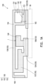
- FIG. 1A is a schematic diagram of an antenna module according to an embodiment of the invention.
- the antenna module 100 of the embodiment may excite at a first frequency band, a second frequency band, and a third frequency band.
- the first frequency band is between 617 MHz and 960 MHz
- the second frequency band is between 1428 MHz and 2690 MHz
- the third frequency band is between 3300 MHz and 4990 MHz.
- the ranges of the first frequency band, the second frequency band, and the third frequency band are not limited thereto.
- the antenna module 100 of the embodiment my meet a full frequency band of Sub-6GHz of LTE.
- the antenna module 100 is described in detail below.
- the antenna module 100 of the embodiment may be in the form of a loop antenna.
- the antenna module 100 includes a feed point 110, a ground plane 120, a main radiator 130 and a parasitic radiator 140.
- the main radiator 130 includes a first portion 131, a second portion 132 and a third portion 133.
- the first portion 131 and the second portion 132 of the main radiator 130 extend in different directions from the feed point 110 and meet at an intersection 134 after turning.
- the first portion 131 and the second portion 132 of the main radiator 130 form a closed loop, such as a rectangle, but a shape of the closed ring is not limited thereto.
- a length of the first portion 131 (the length of a path from the feed point 110 to the right to the intersection 134) of the main radiator 130 is greater than a length of the second portion 132 (the length of a path from the feed point 110 to the left to the intersection 134).
- the maximum width W1 of the first portion 131 is less than the maximum width W2 of the second portion 132.
- a feed signal may travel from the feed point 110 along two paths, the first portion 131 and the second portion 132 of the main radiator 130 until meeting at the intersection. Therefore, the first portion 131 and the second portion 132 of the main radiator 130 may be used to provide two signal paths, so that the first frequency band may achieve a dual-mode effect.
- the third portion 133 includes a first section 135, a second section 136, and a third section 137 connected to the first section 135 and the second section 136.
- the first section 135, the third section 137, and the second section 136 are connected to each other in a bending manner, and present a pattern close to a U-shape.
- the first section 135 of the third portion 133 is connected to the intersection 134, and the second section 136 is connected to the ground plane 120.
- the parasitic radiator 140 is connected to the second section 136 and extends toward the first section 135. In the embodiment, a coupling gap I is kept between the parasitic radiator 140 and the first section 135 of the third portion 133.
- the ground plane 120 includes a first ground portion 122 and a second ground portion 124 separated from each other.
- the first ground portion 122 is close to the second portion 132 of the main radiator 130, and the second ground portion 124 is connected to the third portion 133 of the main radiator 130.
- the first ground portion 122 and the second ground portion 124 are connected to a system ground plane 50.
- the antenna module 100 further includes an extended radiator 150 that extends from the first section 135 of the third portion 133 of the main radiator 130 to perform impedance matching of the first frequency band to achieve a wideband of 617 MHz-960 MHz.
- FIG. 1B is a schematic diagram of a signal path of the antenna module of FIG. 1A exciting at the first frequency band and the second frequency band.
- the feed signal may go along the first portion 131 and the second portion 132 from the feed point 110 and then meet at the intersection 134, and then sequentially go along the third portion 133, the second ground portion 124 of the ground plane 120, the system ground plane 50 and the first ground portion 122 of the ground plane 120 to form a larger loop excitation path.
- the above path may excite at a first frequency band and a second frequency band.
- the second frequency band is a frequency multiplication of the first frequency band. Therefore, the length of the feed signal going along the first portion 131 and the second portion 132 from the feed point 110 and then meeting at the intersection 134, and then sequentially going along the third portion 133 and the ground plane 120 is equivalent to a wavelength of the first frequency band and 1.5 times a wavelength of the second frequency band.
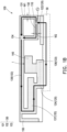
- FIG. 1C is a schematic diagram of a signal path of the antenna module of FIG. 1A exciting at the third frequency band.
- the feed signal may also go along the first portion 131 and the second portion 132 from the feed point 110 and then meet at the intersection 134, and then sequentially go along a part of the first section 135 of the third portion 133, the coupling gap I, the parasitic radiator 140, the second section 136 of the third portion 133, the second ground portion 124 of the ground plane 120, the system ground plane 50, and the first ground portion 122 of the ground plane 120 to form a smaller loop excitation path.
- the above path can excite at a third frequency band.
- a length of the feed signal going along the first portion 131 and the second portion 132 from the feed point 110 and then meeting at the intersection 134, and then sequentially going along a part of the first section 135 of the third portion 133, the coupling gap I, the parasitic radiator 140, the second section 136 of the third portion 133, and the ground plane 50 is equivalent to a wavelength of the third frequency band.
- the antenna module 100 of the embodiment extends from the feed point 110 via the first portion 131 and the second portion 132 of the main radiator 130 and has the intersection 134 far away from the feed point 110.
- the first section 135 of the third portion 133 is connected to the intersection 134, and the second section 136 of the third portion 133 is connected to the ground plane 120.
- the parasitic radiator 140 is connected to the second section 136 and extends toward the first section 135, and may meet a full frequency band of Sub-6GHz of LTE (three bandwidths of a low frequency 617 MHz-960 MHz, an intermediate frequency 1428 MHz-2690 MHz, and a high frequency 3300 MHz-4990 MHz).
- the conventional antenna cannot achieve such wideband, it needs a switch to switch the frequency bands, or it needs to design an antenna that may resonate at different frequency bands according to regulations of different nations, or it needs to use LC components to adjust impedance matching of the antenna to achieve such a wideband. Since the antenna module 100 of the embodiment may reach the full frequency band of Sub-6GHz of LTE, there is no need to arrange additional components to perform switching, and there is no need to use different antennas by nations, which is very convenient in manufacturing.
- FIG. 2 is a schematic diagram of an electronic device according to an embodiment of the invention.
- the electronic device 10 is, for example, a wireless router, but the type of the electronic device 10 is not limited thereto.
- the electronic device 10 includes a heat dissipation conductor 20, an insulating housing 30 and the antenna module 100.
- the heat dissipation conductor 20 is, for example, metal heat dissipation fins
- the insulating housing 30 is, for example, a plastic shell.
- the insulating housing 30 covers at least part of the heat dissipation conductor 20.
- the antenna module 100 is disposed on a circuit board 42, and the circuit board 42 is disposed on the insulating housing 30.
- the ground plane 120 of the antenna module 100 is connected to the heat dissipation conductor 20.
- the heat dissipation conductor 20 is the system ground plane 50 (indicated in FIG. 1A ).
- the conventional antenna requires a sufficient distance from the nearby metal to obtain a sufficient antenna clearance area, so as to prevent the nearby metal from affecting the antenna efficiency
- the heat dissipation conductor 20 of the electronic device 10 may be used as the system ground plane 50 of the antenna. Therefore, the heat dissipation conductor 20 does not affect the antenna efficiency of the antenna module 100, and the distance between the antenna module 100 and the heat dissipation conductor 20 may be reduced.
- a distance between the main radiator 130 (indicated in FIG. 1A ) of the antenna module 100 and the heat dissipation conductor 20 may be, for example, between 2 mm and 20 mm, or even between 2 mm and 10 mm, which may reduce an overall volume of the electronic device 10.
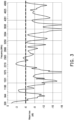
- FIG. 3 is a plot of frequency vs. return loss of the antenna module of FIG. 1A .
- the return losses of the antenna module 100 in the first frequency band, the second frequency band, and the third frequency band may all be lower than -6dB, which achieves a good performance.
- the antenna efficiency of the antenna module 100 in the first frequency band is between 33% and 51%
- the antenna efficiency in the second frequency band is between 39% and 46%
- the antenna efficiency in the third frequency band is between 46% and 57%, which achieves a good performance.
- FIG. 4A to FIG. 4C are antenna pattern diagrams of the antenna module of FIG. 1A in an XZ plane, a YZ plane, and an XY plane when the antenna module is in the first frequency band.
- FIG. 5A to FIG. 5C are antenna pattern diagrams of the antenna module of FIG. 1A in the XZ plane, the YZ plane, and the XY plane when the antenna module is in the second frequency band.
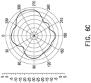
- FIG. 6A to FIG. 6C are antenna pattern diagrams of the antenna module of FIG. 1A in the XZ plane, the YZ plane and the XY plane when the antenna module is in the third frequency band.
- the antenna module 100 of the embodiment has good performance in all of the XZ plane, YZ plane, and XY plane in the first frequency band, the second frequency band, and the third frequency band.
- the first portion and the second portion of the main radiator of the antenna module of the invention extend from the feed point and meet at an intersection far away from the feed point, the first section of the third portion is connected to the intersection, and the second portion of the third portion is connected to the ground plane.
- the parasitic radiator is connected to the second section and extends toward the first section of the third portion.
- the feed signal may go along the first portion and the second portion from the feed point and then meet at the intersection, and then sequentially go along the third portion and the ground plane to excite the first frequency band and the second frequency band.
- the feed signal may go along the first portion and the second portion from the feed point and then meet at the intersection, and then sequentially go along a part of the first section of the third portion, the coupling gap, the parasitic radiator, the second section of the third portion, and the ground plane to excite the third frequency band. Therefore, the antenna module of the invention may have multi-band and wideband effects.
- the antenna module is disposed on the insulating housing, and the ground plane of the antenna module is connected to the heat dissipation conductor, so that the heat dissipation conductor serves as the system ground plane.
- the efficiency of the antenna module is not affected, which achieves an effect of reducing an antenna clearance area.
Landscapes
- Engineering & Computer Science (AREA)
- Computer Networks & Wireless Communication (AREA)
- Variable-Direction Aerials And Aerial Arrays (AREA)
- Details Of Aerials (AREA)
- Support Of Aerials (AREA)
Description
- The invention relates to an antenna module and an electronic device using the antenna module, and particularly relates to a multi-band and wideband antenna module and an electronic device using the antenna module.
- Among the current Netcom products, an LTE frequency band (a low frequency: 704-960 MHz and a high frequency: 1710-2690 MHz) of a fourth-generation communication system is commonly used at present. In response to the advent of a fifth-generation communication system, a bandwidth required by LTE has increased significantly, where the low frequency is 617-960 MHz, which has an increase of nearly 100 MHz, while an intermediate frequency is 1428-2690 MHz, and the high frequency is 3300 MHz-4990 MHz, and a bandwidth of the intermediate-high frequency is increased by about 2000 MHz. The original fourth-generation LTE framework cannot meet the demand for the bandwidth.
- Patent literature
US 2019/123423 A1 proposes an antenna structure including a metal outer cover and an antenna assembly. The metal outer cover has a bent slit. The antenna assembly is stacked on the metal outer cover and covers a portion of the bent slit. The antenna assembly includes a substrate and an antenna pattern disposed on the substrate. The antenna pattern includes a feed end, a first ground end and a second ground end. In the antenna pattern, a first loop and a second loop are formed from the feed end to the first ground end in two respective paths. A third loop is formed from the feed end to the second ground end. The first loop and the third loop resonate with the bent slit to generate a low frequency band and a portion of a high frequency band. The second loop and the third loop resonate with the bent slit to generate another portion of the high frequency band. - Patent literature
US 2012/223867 A1 proposes antenna devices for radio communication devices. The antenna device is adapted for receiving radio signals in a first frequency band and a separate second frequency band. The antenna device includes a half-loop radiating. The first frequency band includes the first harmonic for the half-loop radiating element. The half-loop radiating element includes an inductive loading at a high current section for the third harmonic for the half-loop radiating element, such that the second frequency band includes the third harmonic for the half-loop radiating element. - The invention is directed to an antenna module with multi-band and wideband functions.
- The invention is directed to an electronic device using the above antenna module.
- The invention provides an antenna module including a feed point, a ground plane, a main radiator and a parasitic radiator. The main radiator includes a first portion, a second portion, and a third portion, where the first portion and the second portion extend from the feed point and meet at an intersection after turning. The third portion at least includes a first section and a second section, the first section of the third portion is connected to the intersection, and the second section is connected to the ground plane. The parasitic radiator is connected to the second section and extends towards the first section of the third portion and keeps a coupling gap away from the first section. A feed signal is configured to branch to go along the first portion and the second portion from the feed point and then merge at the intersection, and then sequentially go along the third portion and the ground plane to excite at a first frequency band and a second frequency band. The feed signal is configured to branch to go along the first portion and the second portion from the feed point and then merge at the intersection, and then sequentially go along a part of the first section of the third portion, the coupling gap, the parasitic radiator, the second section of the third portion, and the ground plane to excite at a third frequency band.
- In an embodiment of the invention, the antenna module further includes an extended radiator extending from the third portion to adjust impedance matching of the first frequency band.
- In an embodiment of the invention, a length of the first portion is greater than a length of the second portion, and the maximum width of the first portion is less than the maximum width of the second portion.
- In an embodiment of the invention, the ground plane includes a first ground portion and a second ground portion separated from each other. The first ground portion is close to the second portion, the second ground portion is connected to the third portion, and the first ground portion and the second ground portion are connected to a system ground plane.
- In an embodiment of the invention, the coupling gap is located between the parasitic radiator and the first section of the third portion.
- In an embodiment of the invention, a length of the feed signal respectively passing through the first portion and the second portion from the feed point and then meeting at the intersection, and then sequentially passing through the third portion and the ground plane is equivalent to a wavelength of the first frequency band and 1.5 times a wavelength of the second frequency band.
- In an embodiment of the invention, a length of the feed signal respectively passing through the first portion and the second portion from the feed point and then meeting at the intersection, and then sequentially passing through a part of the first section of the third portion, the coupling gap, the parasitic radiator, the second section of the third portion, and the ground plane is equivalent to a wavelength of the third frequency band.
- In an embodiment of the invention, the first frequency band is between 617 MHz and 960 MHz, the second frequency band is between 1428 MHz and 2690 MHz, and the third frequency band is between 3300 MHz and 4990 MHz.
- The invention provides an electronic device including a heat dissipation conductor, an insulating housing and the antenna module. The insulating housing covers at least part of the heat dissipation conductor. The antenna module is disposed on the insulating housing, where the insulating housing is located between the main radiator of the antenna module and the heat dissipation conductor, and the ground plane of the antenna module is connected to the heat dissipation conductor.
- In an embodiment of the invention, a distance between the main radiator and the heat dissipation conductor is between 2 mm and 20 mm.
- Based on the above description, the first portion and the second portion of the main radiator of the antenna module of the invention extend from the feed point and meet at an intersection far away from the feed point, the first section of the third portion is connected to the intersection, and the second portion of the third portion is connected to the ground plane. The parasitic radiator is connected to the second section and extends toward the first section of the third portion and keeps a coupling gap away from the first section. Based on the above design, the feed signal may go along the first portion and the second portion from the feed point and then meet at the intersection, and then sequentially go along the third portion and the ground plane to excite at the first frequency band and the second frequency band. In addition, the feed signal may go along the first portion and the second portion from the feed point and then meet at the intersection, and then sequentially go along a part of the first section of the third portion, the coupling gap, the parasitic radiator, the second section of the third portion, and the ground plane to excite at the third frequency band. Therefore, the antenna module of the invention may have multi-band and wideband effects.
- In addition, in the electronic device of the invention, the antenna module is arranged on the insulating housing, and the ground plane of the antenna module is connected to the heat dissipation conductor, so that the heat dissipation conductor serves as the system ground plane. In this way, besides that a ground area is increased, even if the antenna module is quite close to the heat dissipation conductor, the efficiency of the antenna module is not affected, which achieves reduction of an antenna clearance area.
- The accompanying drawings are included to provide a further understanding of the invention, and are incorporated in and constitute a part of this specification. The drawings illustrate embodiments of the invention and, together with the description, serve to explain the principles of the invention.
-
FIG. 1A is a schematic diagram of an antenna module according to an embodiment of the invention. -
FIG. 1B is a schematic diagram of a signal path of the antenna module ofFIG. 1A exciting at the first frequency band and the second frequency band. -
FIG. 1C is a schematic diagram of a signal path of the antenna module ofFIG. 1A exciting at a third frequency band. -
FIG. 2 is a schematic diagram of an electronic device according to an embodiment of the invention. -
FIG. 3 is a plot of frequency vs. return loss of the antenna module ofFIG. 1A . -
FIG. 4A to FIG. 4C are antenna pattern diagrams of the antenna module ofFIG. 1A in an XZ plane, a YZ plane, and an XY plane when the antenna module is in a first frequency band. -
FIG. 5A to FIG. 5C are antenna pattern diagrams of the antenna module ofFIG. 1A in the XZ plane, the YZ plane, and the XY plane when the antenna module is in a second frequency band. -
FIG. 6A to FIG. 6C are antenna pattern diagrams of the antenna module ofFIG. 1A in the XZ plane, the YZ plane and the XY plane when the antenna module is in a third frequency band. -
FIG. 1A is a schematic diagram of an antenna module according to an embodiment of the invention. Referring toFIG. 1A , theantenna module 100 of the embodiment may excite at a first frequency band, a second frequency band, and a third frequency band. The first frequency band is between 617 MHz and 960 MHz, the second frequency band is between 1428 MHz and 2690 MHz, and the third frequency band is between 3300 MHz and 4990 MHz. Certainly, the ranges of the first frequency band, the second frequency band, and the third frequency band are not limited thereto. Theantenna module 100 of the embodiment my meet a full frequency band of Sub-6GHz of LTE. Theantenna module 100 is described in detail below. - The
antenna module 100 of the embodiment may be in the form of a loop antenna. Theantenna module 100 includes afeed point 110, aground plane 120, amain radiator 130 and aparasitic radiator 140. Themain radiator 130 includes afirst portion 131, asecond portion 132 and athird portion 133. Thefirst portion 131 and thesecond portion 132 of themain radiator 130 extend in different directions from thefeed point 110 and meet at anintersection 134 after turning. In the embodiment, thefirst portion 131 and thesecond portion 132 of themain radiator 130 form a closed loop, such as a rectangle, but a shape of the closed ring is not limited thereto. - A length of the first portion 131 (the length of a path from the
feed point 110 to the right to the intersection 134) of themain radiator 130 is greater than a length of the second portion 132 (the length of a path from thefeed point 110 to the left to the intersection 134). In addition, the maximum width W1 of thefirst portion 131 is less than the maximum width W2 of thesecond portion 132. - In the embodiment, a feed signal may travel from the
feed point 110 along two paths, thefirst portion 131 and thesecond portion 132 of themain radiator 130 until meeting at the intersection. Therefore, thefirst portion 131 and thesecond portion 132 of themain radiator 130 may be used to provide two signal paths, so that the first frequency band may achieve a dual-mode effect. - The
third portion 133 includes afirst section 135, asecond section 136, and athird section 137 connected to thefirst section 135 and thesecond section 136. In the embodiment, thefirst section 135, thethird section 137, and thesecond section 136 are connected to each other in a bending manner, and present a pattern close to a U-shape. Thefirst section 135 of thethird portion 133 is connected to theintersection 134, and thesecond section 136 is connected to theground plane 120. - The
parasitic radiator 140 is connected to thesecond section 136 and extends toward thefirst section 135. In the embodiment, a coupling gap I is kept between theparasitic radiator 140 and thefirst section 135 of thethird portion 133. - In addition, the
ground plane 120 includes afirst ground portion 122 and asecond ground portion 124 separated from each other. Thefirst ground portion 122 is close to thesecond portion 132 of themain radiator 130, and thesecond ground portion 124 is connected to thethird portion 133 of themain radiator 130. Thefirst ground portion 122 and thesecond ground portion 124 are connected to asystem ground plane 50. - Moreover, the
antenna module 100 further includes anextended radiator 150 that extends from thefirst section 135 of thethird portion 133 of themain radiator 130 to perform impedance matching of the first frequency band to achieve a wideband of 617 MHz-960 MHz. -
FIG. 1B is a schematic diagram of a signal path of the antenna module ofFIG. 1A exciting at the first frequency band and the second frequency band. Referring to bold lines inFIG. 1B , the feed signal may go along thefirst portion 131 and thesecond portion 132 from thefeed point 110 and then meet at theintersection 134, and then sequentially go along thethird portion 133, thesecond ground portion 124 of theground plane 120, thesystem ground plane 50 and thefirst ground portion 122 of theground plane 120 to form a larger loop excitation path. - In the embodiment, the above path may excite at a first frequency band and a second frequency band. The second frequency band is a frequency multiplication of the first frequency band. Therefore, the length of the feed signal going along the
first portion 131 and thesecond portion 132 from thefeed point 110 and then meeting at theintersection 134, and then sequentially going along thethird portion 133 and theground plane 120 is equivalent to a wavelength of the first frequency band and 1.5 times a wavelength of the second frequency band. -
FIG. 1C is a schematic diagram of a signal path of the antenna module ofFIG. 1A exciting at the third frequency band. Referring to the bold lines inFIG. 1C , the feed signal may also go along thefirst portion 131 and thesecond portion 132 from thefeed point 110 and then meet at theintersection 134, and then sequentially go along a part of thefirst section 135 of thethird portion 133, the coupling gap I, theparasitic radiator 140, thesecond section 136 of thethird portion 133, thesecond ground portion 124 of theground plane 120, thesystem ground plane 50, and thefirst ground portion 122 of theground plane 120 to form a smaller loop excitation path. - In the embodiment, the above path can excite at a third frequency band. A length of the feed signal going along the
first portion 131 and thesecond portion 132 from thefeed point 110 and then meeting at theintersection 134, and then sequentially going along a part of thefirst section 135 of thethird portion 133, the coupling gap I, theparasitic radiator 140, thesecond section 136 of thethird portion 133, and theground plane 50 is equivalent to a wavelength of the third frequency band. - Therefore, the
antenna module 100 of the embodiment extends from thefeed point 110 via thefirst portion 131 and thesecond portion 132 of themain radiator 130 and has theintersection 134 far away from thefeed point 110. Thefirst section 135 of thethird portion 133 is connected to theintersection 134, and thesecond section 136 of thethird portion 133 is connected to theground plane 120. Theparasitic radiator 140 is connected to thesecond section 136 and extends toward thefirst section 135, and may meet a full frequency band of Sub-6GHz of LTE (three bandwidths of a low frequency 617 MHz-960 MHz, an intermediate frequency 1428 MHz-2690 MHz, and a high frequency 3300 MHz-4990 MHz). - In the contrast, the conventional antenna cannot achieve such wideband, it needs a switch to switch the frequency bands, or it needs to design an antenna that may resonate at different frequency bands according to regulations of different nations, or it needs to use LC components to adjust impedance matching of the antenna to achieve such a wideband. Since the
antenna module 100 of the embodiment may reach the full frequency band of Sub-6GHz of LTE, there is no need to arrange additional components to perform switching, and there is no need to use different antennas by nations, which is very convenient in manufacturing. -
FIG. 2 is a schematic diagram of an electronic device according to an embodiment of the invention. Referring toFIG. 2 , in the embodiment, theelectronic device 10 is, for example, a wireless router, but the type of theelectronic device 10 is not limited thereto. Theelectronic device 10 includes aheat dissipation conductor 20, an insulatinghousing 30 and theantenna module 100. Theheat dissipation conductor 20 is, for example, metal heat dissipation fins, and the insulatinghousing 30 is, for example, a plastic shell. The insulatinghousing 30 covers at least part of theheat dissipation conductor 20. Theantenna module 100 is disposed on acircuit board 42, and thecircuit board 42 is disposed on the insulatinghousing 30. Theground plane 120 of theantenna module 100 is connected to theheat dissipation conductor 20. - In the embodiment, the
heat dissipation conductor 20 is the system ground plane 50 (indicated inFIG. 1A ). In the contrast, the conventional antenna requires a sufficient distance from the nearby metal to obtain a sufficient antenna clearance area, so as to prevent the nearby metal from affecting the antenna efficiency, in the embodiment, since theground plane 120 of theantenna module 100 is connected to theheat dissipation conductor 20, theheat dissipation conductor 20 of theelectronic device 10 may be used as thesystem ground plane 50 of the antenna. Therefore, theheat dissipation conductor 20 does not affect the antenna efficiency of theantenna module 100, and the distance between theantenna module 100 and theheat dissipation conductor 20 may be reduced. A distance between the main radiator 130 (indicated inFIG. 1A ) of theantenna module 100 and theheat dissipation conductor 20 may be, for example, between 2 mm and 20 mm, or even between 2 mm and 10 mm, which may reduce an overall volume of theelectronic device 10. -
FIG. 3 is a plot of frequency vs. return loss of the antenna module ofFIG. 1A . Referring toFIG. 3 , the return losses of theantenna module 100 in the first frequency band, the second frequency band, and the third frequency band may all be lower than -6dB, which achieves a good performance. In addition, through simulation, in the embodiment, the antenna efficiency of theantenna module 100 in the first frequency band is between 33% and 51%, the antenna efficiency in the second frequency band is between 39% and 46%, and the antenna efficiency in the third frequency band is between 46% and 57%, which achieves a good performance. -
FIG. 4A to FIG. 4C are antenna pattern diagrams of the antenna module ofFIG. 1A in an XZ plane, a YZ plane, and an XY plane when the antenna module is in the first frequency band.FIG. 5A to FIG. 5C are antenna pattern diagrams of the antenna module ofFIG. 1A in the XZ plane, the YZ plane, and the XY plane when the antenna module is in the second frequency band.FIG. 6A to FIG. 6C are antenna pattern diagrams of the antenna module ofFIG. 1A in the XZ plane, the YZ plane and the XY plane when the antenna module is in the third frequency band. - It should be noted that 777 MHz is taken as an example in
FIG. 4A to FIG. 4C , 1995 MHz is taken as an example inFIG. 5A to FIG. 5C , and 3800 MHz is taken as an example inFIG. 6A to FIG. 6C . Referring toFIG. 4A to FIG. 4C ,5A to FIG. 5C , andFIG. 6A to FIG. 6C , theantenna module 100 of the embodiment has good performance in all of the XZ plane, YZ plane, and XY plane in the first frequency band, the second frequency band, and the third frequency band. - In summary, the first portion and the second portion of the main radiator of the antenna module of the invention extend from the feed point and meet at an intersection far away from the feed point, the first section of the third portion is connected to the intersection, and the second portion of the third portion is connected to the ground plane. The parasitic radiator is connected to the second section and extends toward the first section of the third portion. Based on the above design, the feed signal may go along the first portion and the second portion from the feed point and then meet at the intersection, and then sequentially go along the third portion and the ground plane to excite the first frequency band and the second frequency band. In addition, the feed signal may go along the first portion and the second portion from the feed point and then meet at the intersection, and then sequentially go along a part of the first section of the third portion, the coupling gap, the parasitic radiator, the second section of the third portion, and the ground plane to excite the third frequency band. Therefore, the antenna module of the invention may have multi-band and wideband effects.
- In addition, in the electronic device of the invention, the antenna module is disposed on the insulating housing, and the ground plane of the antenna module is connected to the heat dissipation conductor, so that the heat dissipation conductor serves as the system ground plane. In this way, besides that a ground area is increased, even if the antenna module is quite close to the heat dissipation conductor, the efficiency of the antenna module is not affected, which achieves an effect of reducing an antenna clearance area.
Claims (10)
- An antenna module (100), comprising:a feed point (110);a ground plane (120);a main radiator (130), comprising a first portion (131), a second portion (132), and a third portion (133), wherein the first portion (131) and the second portion (132) extend from the feed point (110) and meet at an intersection (134), the third portion (133) at least comprises a first section (135) and a second section (136), the first section (135) of the third portion (133) is connected to the intersection (134), and the second section (136) is connected to the ground plane (120); anda parasitic radiator (140), connected to the second section (136) and extending towards the first section (135) of the third portion (133) and having a coupling gap (I) away from the first section (135), wherein a feed signal is configured to branch at the feed point (110) and go through the first portion (131) and the second portion (132) and then merge at the intersection (134), and then sequentially go along the third portion (133) and the ground plane (120) to excite at a first frequency band and a second frequency band, and go along a part of the first section (135) of the third portion (133), the coupling gap (I), the parasitic radiator (140), the second section (136) of the third portion (133), and the ground plane (120) to excite at a third frequency band.
- The antenna module (100) as claimed in claim 1, further comprising an extended radiator (150) extending from the third portion (133) to adjust impedance matching of the first frequency band.
- The antenna module (100) as claimed in claim 1 or 2, wherein a length of the first portion (131) is greater than a length of the second portion (132), and a maximum width (W1, W2) of the first portion (131) is less than a maximum width (W1, W2) of the second portion (132).
- The antenna module (100) as claimed in claim 1, 2 or 3, wherein the ground plane (120) comprises a first ground portion (122) and a second ground portion (124) separated from each other, the first ground portion (122) is close to the second portion (132), the second ground portion (124) is connected to the third portion (133), and the first ground portion (122) and the second ground portion (124) are connected to a system ground plane (50).
- The antenna module (100) as claimed in claim 1, 2, 3 or 4, wherein the coupling gap (I) is located between the parasitic radiator (140) and the first section (135) of the third portion (133).
- The antenna module (100) as claimed in claim 1, 2, 3, 4 or 5, wherein a length of the feed signal going along the first portion (131) and the second portion (132) from the feed point (110) and then meeting at the intersection (134), and then sequentially going along the third portion (133) and the ground plane (120) is equivalent to a wavelength of the first frequency band and 1.5 times a wavelength of the second frequency band.
- The antenna module (100) as claimed in claim 1, 2, 3, 4, 5 or 6, wherein a length of the feed signal going along the first portion (131) and the second portion (132) from the feed point (110) and then meeting at the intersection (134), and then sequentially going along a part of the first section (135) of the third portion (133), the coupling gap (I), the parasitic radiator (140), the second section (136) of the third portion (133), and the ground plane (120) is equivalent to a wavelength of the third frequency band.
- The antenna module (100) as claimed in claim 1, 2, 3, 4, 5, 6 or 7, wherein the first frequency band is between 617 MHz and 960 MHz, the second frequency band is between 1428 MHz and 2690 MHz, and the third frequency band is between 3300 MHz and 4990 MHz.
- An electronic device (10), comprising:a heat dissipation conductor (20);an insulating housing (30), covering at least part of the heat dissipation conductor (20); andthe antenna module (100) as claimed in any one of claim 1 to claim 8, arranged on the insulating housing (30), wherein the insulating housing (30) is located between the main radiator (130) of the antenna module (100) and the heat dissipation conductor (20), and the ground plane (120) of the antenna module (100) is connected to the heat dissipation conductor (20).
- The electronic device (10) as claimed in claim 9, wherein a distance between the main radiator (130) and the heat dissipation conductor (20) is between 2 mm and 20 mm.
Applications Claiming Priority (1)
| Application Number | Priority Date | Filing Date | Title |
|---|---|---|---|
| TW110104180A TWI745234B (en) | 2021-02-04 | 2021-02-04 | Antenna module and electronic device |
Publications (2)
| Publication Number | Publication Date |
|---|---|
| EP4040597A1 EP4040597A1 (en) | 2022-08-10 |
| EP4040597B1 true EP4040597B1 (en) | 2024-09-25 |
Family
ID=79024773
Family Applications (1)
| Application Number | Title | Priority Date | Filing Date |
|---|---|---|---|
| EP21218067.3A Active EP4040597B1 (en) | 2021-02-04 | 2021-12-29 | Antenna module and electronic device |
Country Status (3)
| Country | Link |
|---|---|
| US (1) | US11682837B2 (en) |
| EP (1) | EP4040597B1 (en) |
| TW (1) | TWI745234B (en) |
Families Citing this family (7)
| Publication number | Priority date | Publication date | Assignee | Title |
|---|---|---|---|---|
| CN114914688B (en) * | 2022-05-17 | 2025-09-16 | 深圳市飞比电子科技有限公司 | Antenna device and intelligent video input device |
| CN218415017U (en) * | 2022-08-09 | 2023-01-31 | 荣耀终端有限公司 | Antenna system and terminal equipment |
| CN115458917B (en) * | 2022-09-28 | 2025-12-30 | 维沃移动通信有限公司 | Antenna structure and electronic equipment |
| CN117855813A (en) * | 2022-10-01 | 2024-04-09 | 华为终端有限公司 | Electronic equipment |
| TWI839953B (en) * | 2022-11-21 | 2024-04-21 | 緯創資通股份有限公司 | Antenna module |
| TWI883628B (en) * | 2023-11-03 | 2025-05-11 | 和碩聯合科技股份有限公司 | Antenna module |
| TWI911681B (en) * | 2024-03-19 | 2026-01-11 | 啓碁科技股份有限公司 | Antenna structure and electronic device |
Family Cites Families (10)
| Publication number | Priority date | Publication date | Assignee | Title |
|---|---|---|---|---|
| TWM383193U (en) | 2010-02-11 | 2010-06-21 | Liang Jih Electric Co Ltd | Press switch device for emergency stop |
| TWI466381B (en) | 2010-10-27 | 2014-12-21 | Acer Inc | Mobile communication device and antenna thereof |
| TWM420055U (en) * | 2011-01-07 | 2012-01-01 | Auden Technology Corp | Antenna structure and electronic product having the antenna structure |
| JP2012160951A (en) * | 2011-02-01 | 2012-08-23 | Toshiba Corp | Multi-resonance antenna device, and electronic apparatus equipped with antenna device |
| EP2495811A1 (en) | 2011-03-01 | 2012-09-05 | Laird Technologies AB | Antenna device and portable radio communication device comprising such antenna device |
| TWM420861U (en) * | 2011-07-22 | 2012-01-11 | Auden Technology Corp | Antenna structure |
| US9172777B2 (en) * | 2013-03-07 | 2015-10-27 | Htc Corporation | Hairpin element for improving antenna bandwidth and antenna efficiency and mobile device with the same |
| KR20160024631A (en) | 2014-08-26 | 2016-03-07 | 삼성전자주식회사 | Multi-band loop antenna and electronic device therewith |
| KR20160090144A (en) * | 2015-01-21 | 2016-07-29 | 주식회사 아모그린텍 | Heat dissipation sheet unified antenna module |
| TWI643402B (en) * | 2017-10-24 | 2018-12-01 | 和碩聯合科技股份有限公司 | Antenna structure and electronic device |
-
2021
- 2021-02-04 TW TW110104180A patent/TWI745234B/en active
- 2021-12-29 EP EP21218067.3A patent/EP4040597B1/en active Active
- 2021-12-29 US US17/565,160 patent/US11682837B2/en active Active
Also Published As
| Publication number | Publication date |
|---|---|
| EP4040597A1 (en) | 2022-08-10 |
| TWI745234B (en) | 2021-11-01 |
| TW202232826A (en) | 2022-08-16 |
| US20220247078A1 (en) | 2022-08-04 |
| US11682837B2 (en) | 2023-06-20 |
Similar Documents
| Publication | Publication Date | Title |
|---|---|---|
| US11682837B2 (en) | Antenna module and electronic device | |
| US10819031B2 (en) | Printed circuit board antenna and terminal | |
| EP2139067B1 (en) | Multiband antenna and radio communication terminal | |
| KR100533624B1 (en) | Multi band chip antenna with dual feeding port, and mobile communication apparatus using the same | |
| EP3767742B1 (en) | Antenna device and mobile terminal | |
| EP2493011B1 (en) | Mobile communication device | |
| CN101304120B (en) | Slot antenna device working under broadband and having stopband | |
| US12166287B2 (en) | Terminal antenna and terminal electronic device | |
| CN101304121B (en) | Slot antenna device acting under broadband at a certain beam width | |
| CN110994196A (en) | Antenna system | |
| JP2006504308A (en) | Wireless device and antenna structure | |
| WO2002071535A1 (en) | Antenna arrangement | |
| KR20070103705A (en) | Multiband antenna | |
| JP2009111999A (en) | Multiband antenna | |
| CN112821038A (en) | Antenna module | |
| CN116315658B (en) | Antenna components and electronic devices | |
| US12444849B2 (en) | Antenna module | |
| KR20010075127A (en) | Antenna which can be operated in several frequency bands | |
| US8947314B2 (en) | Mobile communication device and built-in antenna integrated with a ground portion thereof | |
| CN107112634A (en) | Antenna assembly and communicator | |
| CN113078444A (en) | Antenna structure and wireless communication device with same | |
| CN111755811A (en) | Dual band antenna | |
| CN113078445A (en) | Antenna structure and wireless communication device with same | |
| TWI784726B (en) | Hybrid antenna structure | |
| CN111952714B (en) | Communication assembly and wearable device with same |
Legal Events
| Date | Code | Title | Description |
|---|---|---|---|
| PUAI | Public reference made under article 153(3) epc to a published international application that has entered the european phase |
Free format text: ORIGINAL CODE: 0009012 |
|
| STAA | Information on the status of an ep patent application or granted ep patent |
Free format text: STATUS: THE APPLICATION HAS BEEN PUBLISHED |
|
| AK | Designated contracting states |
Kind code of ref document: A1 Designated state(s): AL AT BE BG CH CY CZ DE DK EE ES FI FR GB GR HR HU IE IS IT LI LT LU LV MC MK MT NL NO PL PT RO RS SE SI SK SM TR |
|
| STAA | Information on the status of an ep patent application or granted ep patent |
Free format text: STATUS: REQUEST FOR EXAMINATION WAS MADE |
|
| 17P | Request for examination filed |
Effective date: 20221014 |
|
| RBV | Designated contracting states (corrected) |
Designated state(s): AL AT BE BG CH CY CZ DE DK EE ES FI FR GB GR HR HU IE IS IT LI LT LU LV MC MK MT NL NO PL PT RO RS SE SI SK SM TR |
|
| GRAP | Despatch of communication of intention to grant a patent |
Free format text: ORIGINAL CODE: EPIDOSNIGR1 |
|
| STAA | Information on the status of an ep patent application or granted ep patent |
Free format text: STATUS: GRANT OF PATENT IS INTENDED |
|
| INTG | Intention to grant announced |
Effective date: 20240510 |
|
| GRAS | Grant fee paid |
Free format text: ORIGINAL CODE: EPIDOSNIGR3 |
|
| GRAA | (expected) grant |
Free format text: ORIGINAL CODE: 0009210 |
|
| STAA | Information on the status of an ep patent application or granted ep patent |
Free format text: STATUS: THE PATENT HAS BEEN GRANTED |
|
| AK | Designated contracting states |
Kind code of ref document: B1 Designated state(s): AL AT BE BG CH CY CZ DE DK EE ES FI FR GB GR HR HU IE IS IT LI LT LU LV MC MK MT NL NO PL PT RO RS SE SI SK SM TR |
|
| REG | Reference to a national code |
Ref country code: GB Ref legal event code: FG4D |
|
| REG | Reference to a national code |
Ref country code: CH Ref legal event code: EP |
|
| REG | Reference to a national code |
Ref country code: DE Ref legal event code: R096 Ref document number: 602021019266 Country of ref document: DE |
|
| REG | Reference to a national code |
Ref country code: IE Ref legal event code: FG4D |
|
| REG | Reference to a national code |
Ref country code: LT Ref legal event code: MG9D |
|
| PG25 | Lapsed in a contracting state [announced via postgrant information from national office to epo] |
Ref country code: NO Free format text: LAPSE BECAUSE OF FAILURE TO SUBMIT A TRANSLATION OF THE DESCRIPTION OR TO PAY THE FEE WITHIN THE PRESCRIBED TIME-LIMIT Effective date: 20241225 |
|
| PG25 | Lapsed in a contracting state [announced via postgrant information from national office to epo] |
Ref country code: GR Free format text: LAPSE BECAUSE OF FAILURE TO SUBMIT A TRANSLATION OF THE DESCRIPTION OR TO PAY THE FEE WITHIN THE PRESCRIBED TIME-LIMIT Effective date: 20241226 Ref country code: FI Free format text: LAPSE BECAUSE OF FAILURE TO SUBMIT A TRANSLATION OF THE DESCRIPTION OR TO PAY THE FEE WITHIN THE PRESCRIBED TIME-LIMIT Effective date: 20240925 |
|
| PG25 | Lapsed in a contracting state [announced via postgrant information from national office to epo] |
Ref country code: BG Free format text: LAPSE BECAUSE OF FAILURE TO SUBMIT A TRANSLATION OF THE DESCRIPTION OR TO PAY THE FEE WITHIN THE PRESCRIBED TIME-LIMIT Effective date: 20240925 |
|
| PG25 | Lapsed in a contracting state [announced via postgrant information from national office to epo] |
Ref country code: LV Free format text: LAPSE BECAUSE OF FAILURE TO SUBMIT A TRANSLATION OF THE DESCRIPTION OR TO PAY THE FEE WITHIN THE PRESCRIBED TIME-LIMIT Effective date: 20240925 |
|
| PG25 | Lapsed in a contracting state [announced via postgrant information from national office to epo] |
Ref country code: RS Free format text: LAPSE BECAUSE OF FAILURE TO SUBMIT A TRANSLATION OF THE DESCRIPTION OR TO PAY THE FEE WITHIN THE PRESCRIBED TIME-LIMIT Effective date: 20241225 |
|
| REG | Reference to a national code |
Ref country code: NL Ref legal event code: MP Effective date: 20240925 |
|
| PG25 | Lapsed in a contracting state [announced via postgrant information from national office to epo] |
Ref country code: RS Free format text: LAPSE BECAUSE OF FAILURE TO SUBMIT A TRANSLATION OF THE DESCRIPTION OR TO PAY THE FEE WITHIN THE PRESCRIBED TIME-LIMIT Effective date: 20241225 Ref country code: NO Free format text: LAPSE BECAUSE OF FAILURE TO SUBMIT A TRANSLATION OF THE DESCRIPTION OR TO PAY THE FEE WITHIN THE PRESCRIBED TIME-LIMIT Effective date: 20241225 Ref country code: LV Free format text: LAPSE BECAUSE OF FAILURE TO SUBMIT A TRANSLATION OF THE DESCRIPTION OR TO PAY THE FEE WITHIN THE PRESCRIBED TIME-LIMIT Effective date: 20240925 Ref country code: GR Free format text: LAPSE BECAUSE OF FAILURE TO SUBMIT A TRANSLATION OF THE DESCRIPTION OR TO PAY THE FEE WITHIN THE PRESCRIBED TIME-LIMIT Effective date: 20241226 Ref country code: FI Free format text: LAPSE BECAUSE OF FAILURE TO SUBMIT A TRANSLATION OF THE DESCRIPTION OR TO PAY THE FEE WITHIN THE PRESCRIBED TIME-LIMIT Effective date: 20240925 Ref country code: BG Free format text: LAPSE BECAUSE OF FAILURE TO SUBMIT A TRANSLATION OF THE DESCRIPTION OR TO PAY THE FEE WITHIN THE PRESCRIBED TIME-LIMIT Effective date: 20240925 |
|
| REG | Reference to a national code |
Ref country code: AT Ref legal event code: MK05 Ref document number: 1727446 Country of ref document: AT Kind code of ref document: T Effective date: 20240925 |
|
| PG25 | Lapsed in a contracting state [announced via postgrant information from national office to epo] |
Ref country code: NL Free format text: LAPSE BECAUSE OF FAILURE TO SUBMIT A TRANSLATION OF THE DESCRIPTION OR TO PAY THE FEE WITHIN THE PRESCRIBED TIME-LIMIT Effective date: 20240925 |
|
| PG25 | Lapsed in a contracting state [announced via postgrant information from national office to epo] |
Ref country code: IS Free format text: LAPSE BECAUSE OF FAILURE TO SUBMIT A TRANSLATION OF THE DESCRIPTION OR TO PAY THE FEE WITHIN THE PRESCRIBED TIME-LIMIT Effective date: 20250125 Ref country code: PT Free format text: LAPSE BECAUSE OF FAILURE TO SUBMIT A TRANSLATION OF THE DESCRIPTION OR TO PAY THE FEE WITHIN THE PRESCRIBED TIME-LIMIT Effective date: 20250127 |
|
| PG25 | Lapsed in a contracting state [announced via postgrant information from national office to epo] |
Ref country code: RO Free format text: LAPSE BECAUSE OF FAILURE TO SUBMIT A TRANSLATION OF THE DESCRIPTION OR TO PAY THE FEE WITHIN THE PRESCRIBED TIME-LIMIT Effective date: 20240925 Ref country code: SM Free format text: LAPSE BECAUSE OF FAILURE TO SUBMIT A TRANSLATION OF THE DESCRIPTION OR TO PAY THE FEE WITHIN THE PRESCRIBED TIME-LIMIT Effective date: 20240925 |
|
| PG25 | Lapsed in a contracting state [announced via postgrant information from national office to epo] |
Ref country code: ES Free format text: LAPSE BECAUSE OF FAILURE TO SUBMIT A TRANSLATION OF THE DESCRIPTION OR TO PAY THE FEE WITHIN THE PRESCRIBED TIME-LIMIT Effective date: 20240925 |
|
| PG25 | Lapsed in a contracting state [announced via postgrant information from national office to epo] |
Ref country code: EE Free format text: LAPSE BECAUSE OF FAILURE TO SUBMIT A TRANSLATION OF THE DESCRIPTION OR TO PAY THE FEE WITHIN THE PRESCRIBED TIME-LIMIT Effective date: 20240925 Ref country code: AT Free format text: LAPSE BECAUSE OF FAILURE TO SUBMIT A TRANSLATION OF THE DESCRIPTION OR TO PAY THE FEE WITHIN THE PRESCRIBED TIME-LIMIT Effective date: 20240925 |
|
| PG25 | Lapsed in a contracting state [announced via postgrant information from national office to epo] |
Ref country code: CZ Free format text: LAPSE BECAUSE OF FAILURE TO SUBMIT A TRANSLATION OF THE DESCRIPTION OR TO PAY THE FEE WITHIN THE PRESCRIBED TIME-LIMIT Effective date: 20240925 Ref country code: PL Free format text: LAPSE BECAUSE OF FAILURE TO SUBMIT A TRANSLATION OF THE DESCRIPTION OR TO PAY THE FEE WITHIN THE PRESCRIBED TIME-LIMIT Effective date: 20240925 |
|
| PG25 | Lapsed in a contracting state [announced via postgrant information from national office to epo] |
Ref country code: SK Free format text: LAPSE BECAUSE OF FAILURE TO SUBMIT A TRANSLATION OF THE DESCRIPTION OR TO PAY THE FEE WITHIN THE PRESCRIBED TIME-LIMIT Effective date: 20240925 |
|
| REG | Reference to a national code |
Ref country code: DE Ref legal event code: R097 Ref document number: 602021019266 Country of ref document: DE |
|
| PG25 | Lapsed in a contracting state [announced via postgrant information from national office to epo] |
Ref country code: MC Free format text: LAPSE BECAUSE OF FAILURE TO SUBMIT A TRANSLATION OF THE DESCRIPTION OR TO PAY THE FEE WITHIN THE PRESCRIBED TIME-LIMIT Effective date: 20240925 |
|
| PG25 | Lapsed in a contracting state [announced via postgrant information from national office to epo] |
Ref country code: DK Free format text: LAPSE BECAUSE OF FAILURE TO SUBMIT A TRANSLATION OF THE DESCRIPTION OR TO PAY THE FEE WITHIN THE PRESCRIBED TIME-LIMIT Effective date: 20240925 |
|
| PGFP | Annual fee paid to national office [announced via postgrant information from national office to epo] |
Ref country code: FR Payment date: 20250602 Year of fee payment: 5 |
|
| PLBE | No opposition filed within time limit |
Free format text: ORIGINAL CODE: 0009261 |
|
| STAA | Information on the status of an ep patent application or granted ep patent |
Free format text: STATUS: NO OPPOSITION FILED WITHIN TIME LIMIT |
|
| PG25 | Lapsed in a contracting state [announced via postgrant information from national office to epo] |
Ref country code: LU Free format text: LAPSE BECAUSE OF NON-PAYMENT OF DUE FEES Effective date: 20241229 |
|
| 26N | No opposition filed |
Effective date: 20250626 |
|
| PG25 | Lapsed in a contracting state [announced via postgrant information from national office to epo] |
Ref country code: SE Free format text: LAPSE BECAUSE OF FAILURE TO SUBMIT A TRANSLATION OF THE DESCRIPTION OR TO PAY THE FEE WITHIN THE PRESCRIBED TIME-LIMIT Effective date: 20240925 |
|
| REG | Reference to a national code |
Ref country code: BE Ref legal event code: MM Effective date: 20241231 |
|
| PG25 | Lapsed in a contracting state [announced via postgrant information from national office to epo] |
Ref country code: BE Free format text: LAPSE BECAUSE OF NON-PAYMENT OF DUE FEES Effective date: 20241231 |
|
| PG25 | Lapsed in a contracting state [announced via postgrant information from national office to epo] |
Ref country code: IE Free format text: LAPSE BECAUSE OF NON-PAYMENT OF DUE FEES Effective date: 20241229 |
|
| REG | Reference to a national code |
Ref country code: CH Ref legal event code: U11 Free format text: ST27 STATUS EVENT CODE: U-0-0-U10-U11 (AS PROVIDED BY THE NATIONAL OFFICE) Effective date: 20260101 |
|
| PGFP | Annual fee paid to national office [announced via postgrant information from national office to epo] |
Ref country code: DE Payment date: 20250612 Year of fee payment: 5 |
|
| PGFP | Annual fee paid to national office [announced via postgrant information from national office to epo] |
Ref country code: IT Payment date: 20251218 Year of fee payment: 5 |
|
| PG25 | Lapsed in a contracting state [announced via postgrant information from national office to epo] |
Ref country code: HR Free format text: LAPSE BECAUSE OF FAILURE TO SUBMIT A TRANSLATION OF THE DESCRIPTION OR TO PAY THE FEE WITHIN THE PRESCRIBED TIME-LIMIT Effective date: 20240925 |
|
| PGFP | Annual fee paid to national office [announced via postgrant information from national office to epo] |
Ref country code: CH Payment date: 20260101 Year of fee payment: 5 |