EP4040483A2 - Electronic component with internal shielding - Google Patents
Electronic component with internal shielding Download PDFInfo
- Publication number
- EP4040483A2 EP4040483A2 EP21216971.8A EP21216971A EP4040483A2 EP 4040483 A2 EP4040483 A2 EP 4040483A2 EP 21216971 A EP21216971 A EP 21216971A EP 4040483 A2 EP4040483 A2 EP 4040483A2
- Authority
- EP
- European Patent Office
- Prior art keywords
- compartment
- separator
- height
- chip
- plane
- Prior art date
- Legal status (The legal status is an assumption and is not a legal conclusion. Google has not performed a legal analysis and makes no representation as to the accuracy of the status listed.)
- Pending
Links
Images


Classifications
-
- H—ELECTRICITY
- H05—ELECTRIC TECHNIQUES NOT OTHERWISE PROVIDED FOR
- H05K—PRINTED CIRCUITS; CASINGS OR CONSTRUCTIONAL DETAILS OF ELECTRIC APPARATUS; MANUFACTURE OF ASSEMBLAGES OF ELECTRICAL COMPONENTS
- H05K9/00—Screening of apparatus or components against electric or magnetic fields
- H05K9/0007—Casings
- H05K9/0049—Casings being metallic containers
-
- H—ELECTRICITY
- H10—SEMICONDUCTOR DEVICES; ELECTRIC SOLID-STATE DEVICES NOT OTHERWISE PROVIDED FOR
- H10W—GENERIC PACKAGES, INTERCONNECTIONS, CONNECTORS OR OTHER CONSTRUCTIONAL DETAILS OF DEVICES COVERED BY CLASS H10
- H10W42/00—Arrangements for protection of devices
- H10W42/20—Arrangements for protection of devices protecting against electromagnetic or particle radiation, e.g. light, X-rays, gamma-rays or electrons
-
- H—ELECTRICITY
- H05—ELECTRIC TECHNIQUES NOT OTHERWISE PROVIDED FOR
- H05K—PRINTED CIRCUITS; CASINGS OR CONSTRUCTIONAL DETAILS OF ELECTRIC APPARATUS; MANUFACTURE OF ASSEMBLAGES OF ELECTRICAL COMPONENTS
- H05K9/00—Screening of apparatus or components against electric or magnetic fields
- H05K9/0007—Casings
- H05K9/002—Casings with localised screening
- H05K9/0022—Casings with localised screening of components mounted on printed circuit boards [PCB]
- H05K9/0024—Shield cases mounted on a PCB, e.g. cans or caps or conformal shields
- H05K9/0026—Shield cases mounted on a PCB, e.g. cans or caps or conformal shields integrally formed from metal sheet
-
- H—ELECTRICITY
- H05—ELECTRIC TECHNIQUES NOT OTHERWISE PROVIDED FOR
- H05K—PRINTED CIRCUITS; CASINGS OR CONSTRUCTIONAL DETAILS OF ELECTRIC APPARATUS; MANUFACTURE OF ASSEMBLAGES OF ELECTRICAL COMPONENTS
- H05K9/00—Screening of apparatus or components against electric or magnetic fields
- H05K9/0007—Casings
- H05K9/002—Casings with localised screening
- H05K9/0022—Casings with localised screening of components mounted on printed circuit boards [PCB]
- H05K9/0037—Housings with compartments containing a PCB, e.g. partitioning walls
-
- H—ELECTRICITY
- H10—SEMICONDUCTOR DEVICES; ELECTRIC SOLID-STATE DEVICES NOT OTHERWISE PROVIDED FOR
- H10W—GENERIC PACKAGES, INTERCONNECTIONS, CONNECTORS OR OTHER CONSTRUCTIONAL DETAILS OF DEVICES COVERED BY CLASS H10
- H10W42/00—Arrangements for protection of devices
- H10W42/20—Arrangements for protection of devices protecting against electromagnetic or particle radiation, e.g. light, X-rays, gamma-rays or electrons
- H10W42/261—Arrangements for protection of devices protecting against electromagnetic or particle radiation, e.g. light, X-rays, gamma-rays or electrons characterised by their shapes or dispositions
- H10W42/273—Arrangements for protection of devices protecting against electromagnetic or particle radiation, e.g. light, X-rays, gamma-rays or electrons characterised by their shapes or dispositions the arrangements being between laterally adjacent chips, e.g. walls between chips
-
- H—ELECTRICITY
- H10—SEMICONDUCTOR DEVICES; ELECTRIC SOLID-STATE DEVICES NOT OTHERWISE PROVIDED FOR
- H10W—GENERIC PACKAGES, INTERCONNECTIONS, CONNECTORS OR OTHER CONSTRUCTIONAL DETAILS OF DEVICES COVERED BY CLASS H10
- H10W76/00—Containers; Fillings or auxiliary members therefor; Seals
- H10W76/60—Seals
-
- H—ELECTRICITY
- H10—SEMICONDUCTOR DEVICES; ELECTRIC SOLID-STATE DEVICES NOT OTHERWISE PROVIDED FOR
- H10W—GENERIC PACKAGES, INTERCONNECTIONS, CONNECTORS OR OTHER CONSTRUCTIONAL DETAILS OF DEVICES COVERED BY CLASS H10
- H10W90/00—Package configurations
-
- H—ELECTRICITY
- H10—SEMICONDUCTOR DEVICES; ELECTRIC SOLID-STATE DEVICES NOT OTHERWISE PROVIDED FOR
- H10W—GENERIC PACKAGES, INTERCONNECTIONS, CONNECTORS OR OTHER CONSTRUCTIONAL DETAILS OF DEVICES COVERED BY CLASS H10
- H10W90/00—Package configurations
- H10W90/701—Package configurations characterised by the relative positions of pads or connectors relative to package parts
- H10W90/721—Package configurations characterised by the relative positions of pads or connectors relative to package parts of bump connectors
- H10W90/724—Package configurations characterised by the relative positions of pads or connectors relative to package parts of bump connectors between a chip and a stacked insulating package substrate, interposer or RDL
-
- H—ELECTRICITY
- H10—SEMICONDUCTOR DEVICES; ELECTRIC SOLID-STATE DEVICES NOT OTHERWISE PROVIDED FOR
- H10W—GENERIC PACKAGES, INTERCONNECTIONS, CONNECTORS OR OTHER CONSTRUCTIONAL DETAILS OF DEVICES COVERED BY CLASS H10
- H10W90/00—Package configurations
- H10W90/701—Package configurations characterised by the relative positions of pads or connectors relative to package parts
- H10W90/721—Package configurations characterised by the relative positions of pads or connectors relative to package parts of bump connectors
- H10W90/726—Package configurations characterised by the relative positions of pads or connectors relative to package parts of bump connectors between a chip and a stacked lead frame, conducting package substrate or heat sink
-
- H—ELECTRICITY
- H10—SEMICONDUCTOR DEVICES; ELECTRIC SOLID-STATE DEVICES NOT OTHERWISE PROVIDED FOR
- H10W—GENERIC PACKAGES, INTERCONNECTIONS, CONNECTORS OR OTHER CONSTRUCTIONAL DETAILS OF DEVICES COVERED BY CLASS H10
- H10W90/00—Package configurations
- H10W90/701—Package configurations characterised by the relative positions of pads or connectors relative to package parts
- H10W90/751—Package configurations characterised by the relative positions of pads or connectors relative to package parts of bond wires
- H10W90/754—Package configurations characterised by the relative positions of pads or connectors relative to package parts of bond wires between a chip and a stacked insulating package substrate, interposer or RDL
-
- H—ELECTRICITY
- H10—SEMICONDUCTOR DEVICES; ELECTRIC SOLID-STATE DEVICES NOT OTHERWISE PROVIDED FOR
- H10W—GENERIC PACKAGES, INTERCONNECTIONS, CONNECTORS OR OTHER CONSTRUCTIONAL DETAILS OF DEVICES COVERED BY CLASS H10
- H10W90/00—Package configurations
- H10W90/701—Package configurations characterised by the relative positions of pads or connectors relative to package parts
- H10W90/751—Package configurations characterised by the relative positions of pads or connectors relative to package parts of bond wires
- H10W90/756—Package configurations characterised by the relative positions of pads or connectors relative to package parts of bond wires between a chip and a stacked lead frame, conducting package substrate or heat sink
Definitions
- the present disclosure relates to shielding of an electronic chip from electromagnetic radiation, and more particularly to shielding the chip from internal radiation generated in other parts of the same component.
- the present disclosure further concerns the use of a metallic cap as a shield.
- Electronic components typically comprise at least one electronic chip and a package.
- the chip is attached to a mounting surface inside the package and may be electrically connected to external devices with electric wires which extend from the chip to external connectors.
- the package provides protection for the electronic chip and it may also shield the chip from external electromagnetic radiation.
- the electronic chip may also be sensitive to electromagnetic radiation emitted by other parts of the electronic component within the same package. These parts may include an adjacent chip or the electric wiring by which chips are connected to external devices.
- An advantage of this arrangement is that internal shielding can be accomplished in a simple manner.
- This disclosure describes an electronic component comprising a package base and a metallic cap.
- the cap is attached to the package base to form an enclosure.
- the electronic component comprises at least one electronic chip which is mounted on a chip-mounting surface in the package base within said enclosure.
- the chip-mounting surface defines a first plane.
- the metallic cap separates the enclosure into at least a first compartment and a second compartment.
- the electronic chip is in the first compartment, and the metallic cap separates the enclosure into the first and second compartments with its shape which forms:
- the term "electronic chip” refers to a unencapsulated electronic device, while “electronic component” refers to an encapsulated device which has been protected from the surrounding environment.
- the electronic chip may be mounted onto a circuit board inside the electronic component.
- the circuit board forms the chip-mounting surface and may contain the control circuits required by the chip. Wires may be drawn from the circuit board or from the chip itself to the outside of the electronic component to facilitate electrical access.
- the electronic component may itself be mounted onto a larger circuit board.
- the electronic chip may for example be a microelectromechanical (MEMS) chip.
- the chip mounting surface defines an xy-plane and the z-axis is perpendicular to this xy-plane.
- the heights mentioned in this disclosure are measured in the direction of the z-axis. Expressions such as “down”, “up”, “above” and “below” correspond to the direction of z-axis illustrated in the figures, which points in the "up” direction. These expressions, and the “heights” discussed below, do not imply anything about how the component should be oriented during use or manufacture.
- the metallic cap may be a continuous metallic sheet.
- the sheet may be shaped into the desired shape by pressing and/or bending the sheet.
- the metallic cap may consist of a metallic material, which may for example be aluminium, copper, an aluminium or copper compound or stainless steel.
- the metallic cap may comprise a polymer foil which has been coated with one of the metallic materials mentioned above, or a moulded plastic body which has been coated with one of the metallic materials mentioned above.
- the continuous metallic sheet may in these cases be a continuous polymer foil or moulded plastic body with a metallic coating.
- the package base may for example be formed by a polymer which has been moulded around the chip-mounting surface.
- the chip-mounting surface may in this case be a die pad which has been formed from a leadframe or a separate support surface which has been attached to the die pad.
- the package base could alternatively be any suitable structure which contains a chip-mounting surface or to which a chip-mounting surface has been attached.
- the distance from the first plane to the first compartment ceiling in the direction perpendicular to the first plane may be called the height of the first compartment.
- the distance from the first plane to the second compartment ceiling in the direction perpendicular to the first plane may be called the height of the second compartment.
- the distance between the first plane and the separator in the direction of the metallic cap is the height of a separator gap.
- Figure 1 illustrates an electronic component 10.
- the component comprises a package base 12 and a metallic cap 11. Together they form an encapsulation around the electronic chip 17 which is mounted on a chip-mounting surface 131.
- the chip-mounting surface defines a first plane 132.
- the first plane 132 and any plane parallel to it, may be called a horizontal plane.
- Directions perpendicular to the first plane may be called vertical.
- the vertical axis is illustrated as the z-axis in figure 1 , and it points in a direction which may be called “up” in this disclosure.
- the opposite direction may be called “down”.
- Words such as “top” and “bottom” may be used with the same meaning. However, these designations are made merely to facilitate convenient references to different directions - they do not imply anything with regard to how the component should be oriented during use or manufacturing.
- the cap 11 and the package base 12 delimit an enclosure, which may also be called a cavity, where the chip 17 and the chip-mounting surface 131 are located.
- the chip-mounting surface may be the floor of this enclosure, so that the first plane and the bottom of the enclosure have the same z-coordinate.
- the chip-mounting surface 131 may be elevated in relation to the bottom of the enclosure 18, so that the first plane 132 and the floor 18 of the enclosure do not have the same z-coordinate.
- the enclosure may be filled with a gas.
- This gas will typically be air, but other gases could also be used.
- the enclosure may be partly or fully filled with an inert and viscous fluid, for example a gel, before the metallic cap is placed on top of it.
- the metallic cap may be a self-supporting cap.
- the metallic cap may be so stiff that when one part of the cap is fixed to a fixing point on the package base, the rest of the cap will also remain fixed in relation to that fixing point.
- figure 1 for example, only the edges (left and right in the figure) of the metallic cap 11 are attached to the package base. The cap supports its own weight, so the central parts of the metallic cap will not be bent or deformed by gravity.
- the metallic cap 11 separates the enclosure into at least a first compartment 141 and a second compartment 142.
- the metallic cap 11 comprises a first sidewall 113 and a second sidewall 114.
- the metallic cap also comprises a first compartment ceiling 111 and a second compartment ceiling 112.
- the vertical distance 151 from the first plane 132 to the first compartment ceiling 111 is the height of the first compartment 141.
- the vertical distance 152 from the first plane 132 to the second compartment ceiling 112 is the height of the second compartment 142.
- the metallic cap also comprises a separator 115 which has been formed between the first compartment ceiling 111 and the second compartment ceiling 112.
- the separator extends downward toward the first plane 132.
- the vertical distance 153 between the lowermost part of the separator 115 and the first plane 132 is the height of the separator gap.
- the separator also extends downward from both the first compartment ceiling 111 and from the second compartment ceiling 112.
- the latter feature extension downward from the second compartment ceiling
- the separator may extend downward only from the first compartment ceiling.
- the first compartment ceiling 111 and second compartment ceiling 112 have been illustrated as horizontals ceilings in figure 1 , but they do not necessarily have to be horizontal. Either one or both could be vertically sloping ceilings.
- the vertical distance 153 is in either case calculated at the border between the first compartment ceiling 111 and the separator 115.
- the separator 115 constitutes an internal shield within the electrical component 11. It may shield the electronic chip 17 from electromagnetic radiation generated in the second compartment 142.
- the device parts which generate electromagnetic radiation in the second compartment 142 may for example include another component or electric wiring (neither of which is illustrated in figure 1 ).
- the separator gap is measured from the first plane to the lower edge of the separator.
- the height of the separator gap may for example be in one of the following ranges, where percentages indicate the ratio between the height of the separator gap and the height of the first compartment: 0% - 90%, 0% - 70%, 0% - 50%, 0% - 30%, 0% - 10%, 1% - 90%, 1% - 70%, 1% - 50%, 1% - 30%, 1% - 10% 10% - 90%, 30% - 90%, 50% - 90%, or 70% - 90%.
- the ratio is 0% if the height of the separator gap is zero.
- a separator gap equal to zero means that the separator 115 reaches all the way down to the first plane 132.
- the separator comes into direct contact with the chip-mounting surface.
- the chip-mounting surface may in some cases not pass under the separator 115.
- the separator 115 may then extend below the first plane 132.
- the distance between the first plane and the separator is defined in the direction of the metallic cap - that is, it is the vertical distance from the first plane to the separator in the direction which points upward from the first plane 132 in figure 1 . This means that if the separator 115 extends below the first plane 132, the height of the separator gap is negative.
- the first and second sidewalls 113 and 114 may be attached to the package base 12, or to any structure on the top surface of the package base, to form the enclosure.
- the metallic cap 11 may comprise additional sidewalls (not illustrated) which allow the cap 11 to be attached to the package base 12 around the perimeter of the package base so that the enclosure is delimited by the package base 12 and the metallic cap 11 on all sides.
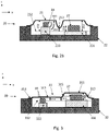
- Figures 2a and 2b illustrate an electronic component where reference numbers 20, 21, 215, 22, 231 - 232, 241 - 242, 251 - 253 and 27 correspond to reference numbers 10, 11, 115, 12, 131 - 132, 141 - 142, 151 - 153 and 17, respectively, in figure 1 .
- the chip-mounting surface 231 here extends from the first compartment 241 to the second compartment 242.
- An emitting device part 28 which lies on the chip-mounting surface 231 in the second compartment 242 emits electromagnetic radiation 281 which could disturb the electronic chip 27.
- the height of the separator gap may be greater than zero, and the height of the second compartment may be greater than the height of the separator gap. This option has already ben illustrated in figures 1 and 2a - 2b above.
- the height of the separator gap may be greater than zero, and the height of the second compartment may be substantially equal to the height of the separator gap.
- Figure 3 illustrates an electronic component where reference numbers 30, 31, 311 - 315, 331 - 333, 351 - 353, 37 and 38 correspond to reference numbers 10, 11, 111 - 115, 131 - 133, 151 - 153 and 17, respectively, in figure 1 .
- the height of the second compartment 352 is in this case substantially equal to the height of the separator gap 353. Due to the shape of the cap 31 and the presence of the separator 315, the impact of internal electromagnetic radiation on the electronic chip will be here also be reduced compared to a situation where the first and second compartment would be equally high and no separator would be present.
- the chip-mounting surface may extend from the first compartment to the second compartment, and the chip-mounting surface may be a circuit board. Furthermore, wires which provide a communication interface connection to the electronic chip may be attached to the circuit board in the second compartment.
- the communication interface can transmit data to and from the circuit board. It may for example be a serial-peripheral interface (SPI), an inter-integrated circuit (I 2 C) interface or a peripheral sensor interface (PSI5).
- SPI serial-peripheral interface
- I 2 C inter-integrated circuit
- PSI5 peripheral sensor interface
- Figure 4 illustrates an electronic component where reference numbers 40, 41, 415, 42, 431 - 432, 453 and 47 correspond to reference numbers 10, 11, 115, 12, 131 - 132, 153 and 17, respectively, in figure 1 .
- the chip-mounting surface 431 is in this case a circuit board to which wiring 49 is attached.
- This wiring 49 may extend outside of the enclosure as figure 4 illustrates (not necessarily in the vertical direction).
- the wiring 49 has been built on the circuit board so that it is located in the second compartment 442 when the metallic cap 41 is placed over the package base 42.
- the cap will then provide internal shielding for the electronic chip 47 from electromagnetic radiation emitted by the wiring 49.
- the wiring may for example include a communication interface to the circuit board which the chip has been mounted on, or any other wires which may emit so much electromagnetic radiation that disturbances are possible in the electronic chip 47.
- FIG. 5 illustrates an electronic component where reference numbers 50, 51, 511 - 515, 531, 532, 551 - 553 and 57 correspond to reference numbers 10, 11, 111 - 115, 131, 132, 151 - 153 and 17, respectively, in figure 1 .
- Reference numbers 58 and 533 correspond to reference numbers 38 and 333, respectively, in figure 3a. This arrangement may be convenient in devices where the chip-mounting surface 131 extends high above the floor 521 of the enclosure.
- the separator 515 may extend to the floor of the enclosure.
- a separator - floor gap may be defined as the vertical distance from the floor 521 of the enclosure to the lowest part of the separator 515.
- the height of this separator - floor gap then for example be in one of the following ranges: 0% - 90%, 0% - 70%, 0% - 50%, 0% - 30%, 0% - 10%, 1% - 90%, 1% - 70%, 1% - 50%, 1% - 30%, 1% - 10% 10% - 90%, 30% - 90%, 50% - 90%, or 70% - 90%, where the percentages indicate the ratio between the height of the separator-floor gap and the height of the chip-mounting surface 531.
- the height of the chip-mounting surface 531 is the vertical distance from the floor 521 to the first plane 532.
Landscapes
- Engineering & Computer Science (AREA)
- Microelectronics & Electronic Packaging (AREA)
- Shielding Devices Or Components To Electric Or Magnetic Fields (AREA)
- Structures Or Materials For Encapsulating Or Coating Semiconductor Devices Or Solid State Devices (AREA)
Abstract
Description
- The present disclosure relates to shielding of an electronic chip from electromagnetic radiation, and more particularly to shielding the chip from internal radiation generated in other parts of the same component. The present disclosure further concerns the use of a metallic cap as a shield.
- Electronic components typically comprise at least one electronic chip and a package. The chip is attached to a mounting surface inside the package and may be electrically connected to external devices with electric wires which extend from the chip to external connectors. The package provides protection for the electronic chip and it may also shield the chip from external electromagnetic radiation.
- However, the electronic chip may also be sensitive to electromagnetic radiation emitted by other parts of the electronic component within the same package. These parts may include an adjacent chip or the electric wiring by which chips are connected to external devices.
- Document
US2012025356 discloses an electronic component where an internal barrier is formed inside an electronic component to separate the component into neighbouring compartments which are shielded from each other. - This disclosure describes an arrangement which is characterized by what is stated in the independent claim. The preferred embodiments of the disclosure are disclosed in the dependent claims. The disclosure is based on the idea of forming a metallic cap into a shape which divides the underlying enclosure into shielded compartments when the cap is placed over a chip to form an enclosed electronic component.
- An advantage of this arrangement is that internal shielding can be accomplished in a simple manner.
- In the following the disclosure will be described in greater detail by means of preferred embodiments with reference to the accompanying drawings, in which
-
Figure 1 illustrates an electronic component with a cap which forms a separator. -
Figure 2a illustrates an electronic component with a chip-mounting surface which extends from the first compartment to the second compartment. -
Figure 2b illustrates an electronic component with a chip-mounting surface which is restricted to the first compartment. -
Figure 3 illustrates an electronic component where the height of the second.compartment is equal to the height of the separator gap. -
Figure 4 illustrates an electronic component where the chip-mounting surface is a circuit board to which wiring is attached. -
Figure 5 illustrates an electronic component where the separator extends below the first plane. - This disclosure describes an electronic component comprising a package base and a metallic cap. The cap is attached to the package base to form an enclosure. The electronic component comprises at least one electronic chip which is mounted on a chip-mounting surface in the package base within said enclosure. The chip-mounting surface defines a first plane.
- The metallic cap separates the enclosure into at least a first compartment and a second compartment. The electronic chip is in the first compartment, and the metallic cap separates the enclosure into the first and second compartments with its shape which forms:
- at least one first sidewall and a first compartment ceiling joined to the at least one first sidewall,
- at least one second sidewall and a second compartment ceiling joined to the at least one second sidewall,
- at least one separator which extends between the first compartment ceiling and the second compartment ceiling, wherein the separator extends from the first compartment ceiling toward the first plane.
- In this disclosure, the term "electronic chip" refers to a unencapsulated electronic device, while "electronic component" refers to an encapsulated device which has been protected from the surrounding environment. The electronic chip may be mounted onto a circuit board inside the electronic component. The circuit board forms the chip-mounting surface and may contain the control circuits required by the chip. Wires may be drawn from the circuit board or from the chip itself to the outside of the electronic component to facilitate electrical access. The electronic component may itself be mounted onto a larger circuit board. The electronic chip may for example be a microelectromechanical (MEMS) chip.
- In the figures of this disclosure, the chip mounting surface defines an xy-plane and the z-axis is perpendicular to this xy-plane. The heights mentioned in this disclosure are measured in the direction of the z-axis. Expressions such as "down", "up", "above" and "below" correspond to the direction of z-axis illustrated in the figures, which points in the "up" direction. These expressions, and the "heights" discussed below, do not imply anything about how the component should be oriented during use or manufacture.
- The metallic cap may be a continuous metallic sheet. The sheet may be shaped into the desired shape by pressing and/or bending the sheet. The metallic cap may consist of a metallic material, which may for example be aluminium, copper, an aluminium or copper compound or stainless steel. Alternatively, the metallic cap may comprise a polymer foil which has been coated with one of the metallic materials mentioned above, or a moulded plastic body which has been coated with one of the metallic materials mentioned above. The continuous metallic sheet may in these cases be a continuous polymer foil or moulded plastic body with a metallic coating.
- The package base may for example be formed by a polymer which has been moulded around the chip-mounting surface. The chip-mounting surface may in this case be a die pad which has been formed from a leadframe or a separate support surface which has been attached to the die pad. The package base could alternatively be any suitable structure which contains a chip-mounting surface or to which a chip-mounting surface has been attached.
- The distance from the first plane to the first compartment ceiling in the direction perpendicular to the first plane may be called the height of the first compartment. The distance from the first plane to the second compartment ceiling in the direction perpendicular to the first plane may be called the height of the second compartment. The distance between the first plane and the separator in the direction of the metallic cap is the height of a separator gap.
-
Figure 1 illustrates anelectronic component 10. The component comprises apackage base 12 and ametallic cap 11. Together they form an encapsulation around theelectronic chip 17 which is mounted on a chip-mounting surface 131. The chip-mounting surface defines afirst plane 132. Thefirst plane 132, and any plane parallel to it, may be called a horizontal plane. Directions perpendicular to the first plane may be called vertical. The vertical axis is illustrated as the z-axis infigure 1 , and it points in a direction which may be called "up" in this disclosure. The opposite direction may be called "down". Words such as "top" and "bottom" may be used with the same meaning. However, these designations are made merely to facilitate convenient references to different directions - they do not imply anything with regard to how the component should be oriented during use or manufacturing. - The
cap 11 and thepackage base 12 delimit an enclosure, which may also be called a cavity, where thechip 17 and the chip-mounting surface 131 are located. The chip-mounting surface may be the floor of this enclosure, so that the first plane and the bottom of the enclosure have the same z-coordinate. Alternatively, asfigure 1 illustrates, the chip-mountingsurface 131 may be elevated in relation to the bottom of theenclosure 18, so that thefirst plane 132 and thefloor 18 of the enclosure do not have the same z-coordinate. - In all embodiments presented in this disclosure, the enclosure may be filled with a gas. This gas will typically be air, but other gases could also be used. Alternatively, the enclosure may be partly or fully filled with an inert and viscous fluid, for example a gel, before the metallic cap is placed on top of it.
- In all embodiments presented in this disclosure, the metallic cap may be a self-supporting cap. In other words, the metallic cap may be so stiff that when one part of the cap is fixed to a fixing point on the package base, the rest of the cap will also remain fixed in relation to that fixing point. In
figure 1 for example, only the edges (left and right in the figure) of themetallic cap 11 are attached to the package base. The cap supports its own weight, so the central parts of the metallic cap will not be bent or deformed by gravity. - The
metallic cap 11 separates the enclosure into at least afirst compartment 141 and asecond compartment 142. Themetallic cap 11 comprises afirst sidewall 113 and asecond sidewall 114. The metallic cap also comprises afirst compartment ceiling 111 and asecond compartment ceiling 112. Thevertical distance 151 from thefirst plane 132 to thefirst compartment ceiling 111 is the height of thefirst compartment 141. Thevertical distance 152 from thefirst plane 132 to thesecond compartment ceiling 112 is the height of thesecond compartment 142. - The metallic cap also comprises a
separator 115 which has been formed between thefirst compartment ceiling 111 and thesecond compartment ceiling 112. The separator extends downward toward thefirst plane 132. Thevertical distance 153 between the lowermost part of theseparator 115 and thefirst plane 132 is the height of the separator gap. Infigure 1 , the separator also extends downward from both thefirst compartment ceiling 111 and from thesecond compartment ceiling 112. However, as will be explained in more detail below, the latter feature (extension downward from the second compartment ceiling) is optional, and the separator may extend downward only from the first compartment ceiling. - The
first compartment ceiling 111 andsecond compartment ceiling 112 have been illustrated as horizontals ceilings infigure 1 , but they do not necessarily have to be horizontal. Either one or both could be vertically sloping ceilings. Thevertical distance 153 is in either case calculated at the border between thefirst compartment ceiling 111 and theseparator 115. - The
separator 115 constitutes an internal shield within theelectrical component 11. It may shield theelectronic chip 17 from electromagnetic radiation generated in thesecond compartment 142. The device parts which generate electromagnetic radiation in thesecond compartment 142 may for example include another component or electric wiring (neither of which is illustrated infigure 1 ). - The separator gap is measured from the first plane to the lower edge of the separator. The height of the separator gap may for example be in one of the following ranges, where percentages indicate the ratio between the height of the separator gap and the height of the first compartment: 0% - 90%, 0% - 70%, 0% - 50%, 0% - 30%, 0% - 10%, 1% - 90%, 1% - 70%, 1% - 50%, 1% - 30%, 1% - 10% 10% - 90%, 30% - 90%, 50% - 90%, or 70% - 90%.The ratio is 0% if the height of the separator gap is zero. A separator gap equal to zero means that the
separator 115 reaches all the way down to thefirst plane 132. - In some cases, this could mean that the separator comes into direct contact with the chip-mounting surface. On the other hand, the chip-mounting surface may in some cases not pass under the
separator 115. Theseparator 115 may then extend below thefirst plane 132. In this disclosure, the distance between the first plane and the separator is defined in the direction of the metallic cap - that is, it is the vertical distance from the first plane to the separator in the direction which points upward from thefirst plane 132 infigure 1 . This means that if theseparator 115 extends below thefirst plane 132, the height of the separator gap is negative. - The first and
second sidewalls package base 12, or to any structure on the top surface of the package base, to form the enclosure. Themetallic cap 11 may comprise additional sidewalls (not illustrated) which allow thecap 11 to be attached to thepackage base 12 around the perimeter of the package base so that the enclosure is delimited by thepackage base 12 and themetallic cap 11 on all sides. -
Figures 2a and2b illustrate an electronic component wherereference numbers numbers figure 1 . The chip-mountingsurface 231 here extends from thefirst compartment 241 to thesecond compartment 242. An emittingdevice part 28 which lies on the chip-mountingsurface 231 in thesecond compartment 242 emitselectromagnetic radiation 281 which could disturb theelectronic chip 27. - It may in some cases be necessary to maximize the protection of the
electronic chip 27 fromradiation 281 by making the height of theseparator gap 253 zero. However, a zero-height gap is not always necessary. Adequate protection may often be obtained even with a separator gap which is greater than zero because the sensitivity ofelectronic chip 27 to theradiation 281 may be affected by many different variables, such as the height of thecomponent 254, the placement of the emittingdevice part 28 in thesecond compartment 242, and the height of the surfaces wherepart 28 andchip 27 are mounted.Figure 2b illustrates an electronic component where the emitting device part has been mounted on a surface which is clearly higher than thefirst plane 232, which will reduce the exposure of thechip 27 to theradiation 281. - The height of the separator gap may be greater than zero, and the height of the second compartment may be greater than the height of the separator gap. This option has already ben illustrated in
figures 1 and2a - 2b above. - The height of the separator gap may be greater than zero, and the height of the second compartment may be substantially equal to the height of the separator gap.
Figure 3 illustrates an electronic component wherereference numbers numbers figure 1 . The height of thesecond compartment 352 is in this case substantially equal to the height of theseparator gap 353. Due to the shape of thecap 31 and the presence of theseparator 315, the impact of internal electromagnetic radiation on the electronic chip will be here also be reduced compared to a situation where the first and second compartment would be equally high and no separator would be present. - The chip-mounting surface may extend from the first compartment to the second compartment, and the chip-mounting surface may be a circuit board. Furthermore, wires which provide a communication interface connection to the electronic chip may be attached to the circuit board in the second compartment. The communication interface can transmit data to and from the circuit board. It may for example be a serial-peripheral interface (SPI), an inter-integrated circuit (I2C) interface or a peripheral sensor interface (PSI5).
-
Figure 4 illustrates an electronic component wherereference numbers numbers figure 1 . The chip-mountingsurface 431 is in this case a circuit board to whichwiring 49 is attached. Thiswiring 49 may extend outside of the enclosure asfigure 4 illustrates (not necessarily in the vertical direction). Thewiring 49 has been built on the circuit board so that it is located in thesecond compartment 442 when themetallic cap 41 is placed over thepackage base 42. The cap will then provide internal shielding for theelectronic chip 47 from electromagnetic radiation emitted by thewiring 49. As mentioned above, the wiring may for example include a communication interface to the circuit board which the chip has been mounted on, or any other wires which may emit so much electromagnetic radiation that disturbances are possible in theelectronic chip 47. - The separator may extend below the first plane so that the height of the separator gap is negative.
Figure 5 illustrates an electronic component wherereference numbers numbers figure 1 .Reference numbers numbers surface 131 extends high above thefloor 521 of the enclosure. Theseparator 515 may extend to the floor of the enclosure. A separator - floor gap may be defined as the vertical distance from thefloor 521 of the enclosure to the lowest part of theseparator 515. The height of this separator - floor gap then for example be in one of the following ranges: 0% - 90%, 0% - 70%, 0% - 50%, 0% - 30%, 0% - 10%, 1% - 90%, 1% - 70%, 1% - 50%, 1% - 30%, 1% - 10% 10% - 90%, 30% - 90%, 50% - 90%, or 70% - 90%, where the percentages indicate the ratio between the height of the separator-floor gap and the height of the chip-mountingsurface 531. The height of the chip-mountingsurface 531 is the vertical distance from thefloor 521 to thefirst plane 532.
Claims (7)
- An electronic component comprising a package base and a metallic cap which is attached to the package base to form an enclosure, wherein the electronic component comprises at least one electronic chip which is mounted on a chip-mounting surface in the package base within said enclosure, whereby the chip-mounting surface defines a first plane,
characterized in that the metallic cap separates the enclosure into at least a first compartment and a second compartment, and the electronic chip is in the first compartment, and the metallic cap separates the enclosure into the first and second compartments with its shape which forms:- at least one first sidewall and a first compartment ceiling joined to the at least one first sidewall,- at least one second sidewall and a second compartment ceiling joined to the at least one second sidewall,- at least one separator which extends between the first compartment ceiling and the second compartment ceiling, wherein the separator extends from the first compartment ceiling toward the first plane. - An electronic component according to claim 1, characterized in that the distance between the first plane and the separator in the direction of the metallic cap is the height of a separator gap, and the height of the separator gap is substantially zero.
- An electronic component according to claim 1, characterized in that the distance between the first plane and the separator in the direction of the metallic cap is the height of a separator gap, the distance from the first plane to the second compartment ceiling in the direction perpendicular to the first plane is the height of the second compartment, and the height of the separator gap is greater than zero, and the height of the second compartment is substantially equal to the height of the separator gap.
- An electronic component according to claim 1, characterized in that the distance between the first plane and the separator in the direction of the metallic cap is the height of a separator gap, the distance from the first plane to the second compartment ceiling in the direction perpendicular to the first plane is the height of the second compartment, and the height of the separator gap is greater than zero, and the height of the second compartment is greater than the height of the separator gap.
- An electronic component according to any of claims 1-4, characterized in that the chip-mounting surface extends from the first compartment to the second compartment, and the chip-mounting surface is a circuit board.
- An electronic component according to claim 5, characterized in that wires which provide a communication interface connection to the electronic chip are attached to the circuit board in the second compartment.
- An electronic component according to claim 1, characterized in that the distance between the first plane and the separator in the direction of the metallic cap is the height of a separator gap, and the separator extends below the first plane so that the height of the separator gap is negative.
Applications Claiming Priority (1)
| Application Number | Priority Date | Filing Date | Title |
|---|---|---|---|
| FI20215121 | 2021-02-04 |
Publications (2)
| Publication Number | Publication Date |
|---|---|
| EP4040483A2 true EP4040483A2 (en) | 2022-08-10 |
| EP4040483A3 EP4040483A3 (en) | 2022-10-26 |
Family
ID=79316862
Family Applications (1)
| Application Number | Title | Priority Date | Filing Date |
|---|---|---|---|
| EP21216971.8A Pending EP4040483A3 (en) | 2021-02-04 | 2021-12-22 | Electronic component with internal shielding |
Country Status (3)
| Country | Link |
|---|---|
| US (1) | US12075605B2 (en) |
| EP (1) | EP4040483A3 (en) |
| JP (1) | JP7283589B2 (en) |
Families Citing this family (1)
| Publication number | Priority date | Publication date | Assignee | Title |
|---|---|---|---|---|
| CN118315374B (en) * | 2024-06-11 | 2024-10-29 | 甬矽电子(宁波)股份有限公司 | Chip stacking structure and chip packaging method |
Citations (1)
| Publication number | Priority date | Publication date | Assignee | Title |
|---|---|---|---|---|
| US20120025356A1 (en) | 2010-08-02 | 2012-02-02 | Kuo-Hsien Liao | Semiconductor device packages having electromagnetic interference shielding and related methods |
Family Cites Families (28)
| Publication number | Priority date | Publication date | Assignee | Title |
|---|---|---|---|---|
| US20010033478A1 (en) | 2000-04-21 | 2001-10-25 | Shielding For Electronics, Inc. | EMI and RFI shielding for printed circuit boards |
| WO2003049519A1 (en) * | 2001-12-07 | 2003-06-12 | Radiant Networks Plc | Shielding device, circuit assembly and method of manufacture |
| US7643311B2 (en) * | 2005-04-21 | 2010-01-05 | Stmicroelectronics Sa | Electronic circuit protection device |
| DE102005053765B4 (en) | 2005-11-10 | 2016-04-14 | Epcos Ag | MEMS package and method of manufacture |
| US8008753B1 (en) * | 2008-04-22 | 2011-08-30 | Amkor Technology, Inc. | System and method to reduce shorting of radio frequency (RF) shielding |
| US20090266601A1 (en) * | 2008-04-24 | 2009-10-29 | Yu-Jen Cheng | Protective cover for prevention of electromagnetism interference |
| US20090265931A1 (en) * | 2008-04-28 | 2009-10-29 | Yu-Jen Cheng | Method for manufacturing protective cover for prevention of electromagnetism interference |
| US7772046B2 (en) * | 2008-06-04 | 2010-08-10 | Stats Chippac, Ltd. | Semiconductor device having electrical devices mounted to IPD structure and method for shielding electromagnetic interference |
| JP2010177520A (en) | 2009-01-30 | 2010-08-12 | Toshiba Corp | Electronic circuit module and method of manufacturing the same |
| JP2010225620A (en) | 2009-03-19 | 2010-10-07 | Panasonic Corp | Circuit module |
| US9386734B2 (en) * | 2010-08-05 | 2016-07-05 | Epcos Ag | Method for producing a plurality of electronic devices |
| JP5837515B2 (en) | 2011-01-27 | 2015-12-24 | 株式会社村田製作所 | Circuit module |
| JP2013222829A (en) * | 2012-04-17 | 2013-10-28 | Taiyo Yuden Co Ltd | Circuit module and manufacturing method thereof |
| JP6004001B2 (en) * | 2012-10-29 | 2016-10-05 | 富士電機株式会社 | Semiconductor device |
| TWI509767B (en) * | 2013-12-13 | 2015-11-21 | 環旭電子股份有限公司 | Electronic package module and manufacturing method thereof |
| US20170090532A1 (en) * | 2014-03-14 | 2017-03-30 | Kaneka Corporation | Electronic terminal equipment and method for assembling same |
| JP6387278B2 (en) * | 2014-09-30 | 2018-09-05 | 太陽誘電株式会社 | Circuit module and manufacturing method thereof |
| US10292258B2 (en) * | 2015-03-26 | 2019-05-14 | Apple Inc. | Vertical shielding and interconnect for SIP modules |
| WO2017145331A1 (en) * | 2016-02-25 | 2017-08-31 | 三菱電機株式会社 | Semiconductor package and module |
| JP6621708B2 (en) | 2016-05-26 | 2019-12-18 | 新光電気工業株式会社 | Semiconductor device and method for manufacturing semiconductor device |
| JP2018064044A (en) * | 2016-10-13 | 2018-04-19 | イビデン株式会社 | Shield cap and manufacturing method thereof |
| WO2019005171A1 (en) * | 2017-06-30 | 2019-01-03 | Intel Corporation | Enclosure for an electronic component |
| JP7136553B2 (en) | 2017-12-08 | 2022-09-13 | 日立Astemo株式会社 | electronic controller |
| WO2019135376A1 (en) * | 2018-01-05 | 2019-07-11 | 株式会社村田製作所 | High-frequency module |
| JP7158463B2 (en) * | 2018-03-23 | 2022-10-21 | 日立Astemo株式会社 | electronic controller |
| US20200203287A1 (en) | 2018-12-20 | 2020-06-25 | Qualcomm Incorporated | Device comprising compartmental shielding with improved heat dissipation and routing |
| US20200359534A1 (en) * | 2019-05-09 | 2020-11-12 | Intel Corporation | Radio frequency/electromagnetic interference shielding sructures containing plastic materials |
| US20230156932A1 (en) * | 2019-10-17 | 2023-05-18 | Nippon Telegraph And Telephone Corporation | Optical Communication Element |
-
2021
- 2021-12-22 EP EP21216971.8A patent/EP4040483A3/en active Pending
-
2022
- 2022-01-10 US US17/572,073 patent/US12075605B2/en active Active
- 2022-01-27 JP JP2022010929A patent/JP7283589B2/en active Active
Patent Citations (1)
| Publication number | Priority date | Publication date | Assignee | Title |
|---|---|---|---|---|
| US20120025356A1 (en) | 2010-08-02 | 2012-02-02 | Kuo-Hsien Liao | Semiconductor device packages having electromagnetic interference shielding and related methods |
Also Published As
| Publication number | Publication date |
|---|---|
| EP4040483A3 (en) | 2022-10-26 |
| JP7283589B2 (en) | 2023-05-30 |
| JP2022119735A (en) | 2022-08-17 |
| US12075605B2 (en) | 2024-08-27 |
| US20220248576A1 (en) | 2022-08-04 |
Similar Documents
| Publication | Publication Date | Title |
|---|---|---|
| US20230197769A1 (en) | Semiconductor device and method of manufacturing a semiconductor device | |
| CN101919053B (en) | Integrated circuit package having integrated faraday shield | |
| TWI529827B (en) | Integrated circuit package system with package stack and manufacturing method thereof | |
| US20080185692A1 (en) | Package-level electromagnetic interference shielding | |
| US20070296069A1 (en) | Semiconductor apparatus with decoupling capacitor | |
| EP3407378B1 (en) | Semiconductor package and module | |
| KR20030024157A (en) | Power semiconductor module that has three dimensional structure and a method of manufacturing thereof | |
| US12075605B2 (en) | Electronic component with internal shielding | |
| WO2019089769A1 (en) | Electromagnetic interference shield within integrated circuit encapsulation using photonic bandgap structure | |
| CN107180825B (en) | Semiconductor package with barrier for RF absorber | |
| US20060091517A1 (en) | Stacked semiconductor multi-chip package | |
| EP3648158A1 (en) | Shielded semiconductor device and lead frame therefor | |
| EP2869337A2 (en) | Electrical assembly with a solder sphere attached heat spreader | |
| CN100461392C (en) | semiconductor package | |
| US20260076209A1 (en) | Electromagnetic interference shielding package structures and fabricating methods thereof | |
| US20090260872A1 (en) | Module for packaging electronic components by using a cap | |
| CN112956090A (en) | Quad flat no-lead package for side-emitting laser diode | |
| CN221125945U (en) | Chip packaging structure and electronic equipment | |
| US20200273810A1 (en) | Semiconductor device with integral emi shield | |
| CN114864568B (en) | Packaging structure and display device | |
| US20210035916A1 (en) | Semiconductor package | |
| GB2292003A (en) | Direct chip attach | |
| US12075603B2 (en) | Shielded electronic component | |
| US12557658B2 (en) | Molded module package with an EMI shielding barrier | |
| US20250022846A1 (en) | Multi-chip package device |
Legal Events
| Date | Code | Title | Description |
|---|---|---|---|
| PUAI | Public reference made under article 153(3) epc to a published international application that has entered the european phase |
Free format text: ORIGINAL CODE: 0009012 |
|
| STAA | Information on the status of an ep patent application or granted ep patent |
Free format text: STATUS: REQUEST FOR EXAMINATION WAS MADE |
|
| 17P | Request for examination filed |
Effective date: 20211222 |
|
| AK | Designated contracting states |
Kind code of ref document: A2 Designated state(s): AL AT BE BG CH CY CZ DE DK EE ES FI FR GB GR HR HU IE IS IT LI LT LU LV MC MK MT NL NO PL PT RO RS SE SI SK SM TR |
|
| PUAL | Search report despatched |
Free format text: ORIGINAL CODE: 0009013 |
|
| AK | Designated contracting states |
Kind code of ref document: A3 Designated state(s): AL AT BE BG CH CY CZ DE DK EE ES FI FR GB GR HR HU IE IS IT LI LT LU LV MC MK MT NL NO PL PT RO RS SE SI SK SM TR |
|
| RIC1 | Information provided on ipc code assigned before grant |
Ipc: H05K 9/00 20060101ALI20220920BHEP Ipc: H01L 23/10 20060101ALI20220920BHEP Ipc: H01L 23/552 20060101AFI20220920BHEP |