EP4040144A1 - Analyzer and image processing method - Google Patents
Analyzer and image processing method Download PDFInfo
- Publication number
- EP4040144A1 EP4040144A1 EP22154930.6A EP22154930A EP4040144A1 EP 4040144 A1 EP4040144 A1 EP 4040144A1 EP 22154930 A EP22154930 A EP 22154930A EP 4040144 A1 EP4040144 A1 EP 4040144A1
- Authority
- EP
- European Patent Office
- Prior art keywords
- image
- positional deviation
- partial
- images
- measurement
- Prior art date
- Legal status (The legal status is an assumption and is not a legal conclusion. Google has not performed a legal analysis and makes no representation as to the accuracy of the status listed.)
- Granted
Links
Images






Classifications
-
- G—PHYSICS
- G01—MEASURING; TESTING
- G01N—INVESTIGATING OR ANALYSING MATERIALS BY DETERMINING THEIR CHEMICAL OR PHYSICAL PROPERTIES
- G01N23/00—Investigating or analysing materials by the use of wave or particle radiation, e.g. X-rays or neutrons, not covered by groups G01N3/00 – G01N17/00, G01N21/00 or G01N22/00
- G01N23/22—Investigating or analysing materials by the use of wave or particle radiation, e.g. X-rays or neutrons, not covered by groups G01N3/00 – G01N17/00, G01N21/00 or G01N22/00 by measuring secondary emission from the material
- G01N23/225—Investigating or analysing materials by the use of wave or particle radiation, e.g. X-rays or neutrons, not covered by groups G01N3/00 – G01N17/00, G01N21/00 or G01N22/00 by measuring secondary emission from the material using electron or ion
- G01N23/2251—Investigating or analysing materials by the use of wave or particle radiation, e.g. X-rays or neutrons, not covered by groups G01N3/00 – G01N17/00, G01N21/00 or G01N22/00 by measuring secondary emission from the material using electron or ion using incident electron beams, e.g. scanning electron microscopy [SEM]
- G01N23/2252—Measuring emitted X-rays, e.g. electron probe microanalysis [EPMA]
-
- G—PHYSICS
- G06—COMPUTING OR CALCULATING; COUNTING
- G06T—IMAGE DATA PROCESSING OR GENERATION, IN GENERAL
- G06T7/00—Image analysis
- G06T7/30—Determination of transform parameters for the alignment of images, i.e. image registration
- G06T7/33—Determination of transform parameters for the alignment of images, i.e. image registration using feature-based methods
-
- H—ELECTRICITY
- H01—ELECTRIC ELEMENTS
- H01J—ELECTRIC DISCHARGE TUBES OR DISCHARGE LAMPS
- H01J37/00—Discharge tubes with provision for introducing objects or material to be exposed to the discharge, e.g. for the purpose of examination or processing thereof
- H01J37/02—Details
- H01J37/22—Optical, image processing or photographic arrangements associated with the tube
- H01J37/222—Image processing arrangements associated with the tube
-
- H—ELECTRICITY
- H01—ELECTRIC ELEMENTS
- H01J—ELECTRIC DISCHARGE TUBES OR DISCHARGE LAMPS
- H01J37/00—Discharge tubes with provision for introducing objects or material to be exposed to the discharge, e.g. for the purpose of examination or processing thereof
- H01J37/02—Details
- H01J37/22—Optical, image processing or photographic arrangements associated with the tube
- H01J37/226—Optical arrangements for illuminating the object; optical arrangements for collecting light from the object
-
- G—PHYSICS
- G01—MEASURING; TESTING
- G01N—INVESTIGATING OR ANALYSING MATERIALS BY DETERMINING THEIR CHEMICAL OR PHYSICAL PROPERTIES
- G01N2223/00—Investigating materials by wave or particle radiation
- G01N2223/40—Imaging
- G01N2223/401—Imaging image processing
-
- G—PHYSICS
- G01—MEASURING; TESTING
- G01N—INVESTIGATING OR ANALYSING MATERIALS BY DETERMINING THEIR CHEMICAL OR PHYSICAL PROPERTIES
- G01N2223/00—Investigating materials by wave or particle radiation
- G01N2223/40—Imaging
- G01N2223/402—Imaging mapping distribution of elements
-
- G—PHYSICS
- G01—MEASURING; TESTING
- G01N—INVESTIGATING OR ANALYSING MATERIALS BY DETERMINING THEIR CHEMICAL OR PHYSICAL PROPERTIES
- G01N2223/00—Investigating materials by wave or particle radiation
- G01N2223/40—Imaging
- G01N2223/418—Imaging electron microscope
-
- G—PHYSICS
- G01—MEASURING; TESTING
- G01N—INVESTIGATING OR ANALYSING MATERIALS BY DETERMINING THEIR CHEMICAL OR PHYSICAL PROPERTIES
- G01N2223/00—Investigating materials by wave or particle radiation
- G01N2223/60—Specific applications or type of materials
- G01N2223/605—Specific applications or type of materials phases
-
- G—PHYSICS
- G06—COMPUTING OR CALCULATING; COUNTING
- G06T—IMAGE DATA PROCESSING OR GENERATION, IN GENERAL
- G06T2207/00—Indexing scheme for image analysis or image enhancement
- G06T2207/10—Image acquisition modality
- G06T2207/10056—Microscopic image
-
- G—PHYSICS
- G06—COMPUTING OR CALCULATING; COUNTING
- G06T—IMAGE DATA PROCESSING OR GENERATION, IN GENERAL
- G06T2207/00—Indexing scheme for image analysis or image enhancement
- G06T2207/10—Image acquisition modality
- G06T2207/10116—X-ray image
-
- G—PHYSICS
- G06—COMPUTING OR CALCULATING; COUNTING
- G06T—IMAGE DATA PROCESSING OR GENERATION, IN GENERAL
- G06T2207/00—Indexing scheme for image analysis or image enhancement
- G06T2207/20—Special algorithmic details
- G06T2207/20016—Hierarchical, coarse-to-fine, multiscale or multiresolution image processing; Pyramid transform
-
- G—PHYSICS
- G06—COMPUTING OR CALCULATING; COUNTING
- G06T—IMAGE DATA PROCESSING OR GENERATION, IN GENERAL
- G06T2207/00—Indexing scheme for image analysis or image enhancement
- G06T2207/20—Special algorithmic details
- G06T2207/20021—Dividing image into blocks, subimages or windows
-
- H—ELECTRICITY
- H01—ELECTRIC ELEMENTS
- H01J—ELECTRIC DISCHARGE TUBES OR DISCHARGE LAMPS
- H01J2237/00—Discharge tubes exposing object to beam, e.g. for analysis treatment, etching, imaging
- H01J2237/22—Treatment of data
- H01J2237/221—Image processing
-
- H—ELECTRICITY
- H01—ELECTRIC ELEMENTS
- H01J—ELECTRIC DISCHARGE TUBES OR DISCHARGE LAMPS
- H01J2237/00—Discharge tubes exposing object to beam, e.g. for analysis treatment, etching, imaging
- H01J2237/26—Electron or ion microscopes
- H01J2237/28—Scanning microscopes
- H01J2237/2809—Scanning microscopes characterised by the imaging problems involved
Definitions
- An electron probe micro-analyzer (EPMA) is known, which analyzes a specimen by applying an electron beam to the surface of the specimen and spectrally detecting a characteristic X-ray emitted from the specimen.
- the EPMA is normally equipped with a plurality of wavelength dispersive X-ray spectrometers (WDS).
- WDS wavelength dispersive X-ray spectrometers
- a positional deviation may be generated among the X-ray maps due to the drift of the specimen and the like. If a positional deviation is generated among the X-ray maps, the correlation of the elements cannot be correctly analyzed in the phase analysis, for example.
- JP-A-2012-149910 in a case where data of each X-ray image (X-ray map) on a same region of a specimen is acquired and stored at different timings, by using an EPMA: an electron image data based on detected secondary electrons or back-scattered electrons is also acquired for the region at each timing; then a positional deviation amount is calculated by comparing the electron image data acquired at different timings; and based on the calculated positional deviation amount, a region that commonly exists in the data of each X-ray image acquired at different timings is extracted.
- an analyzer including:
- the electron optical system 10 forms an electron probe constituted of focused electron beam EB.
- the electron optical system 10 includes an electron gun 12, a focusing lens 14, a deflector 16 and an objective lens 18.
- FIG. 3 is a block diagram illustrating a configuration of the image processor 4.
- the display unit 72 displays an image generated by the processing unit 60.
- the display unit 72 is implemented by such a display as a liquid crystal display (LCD), for example.
- LCD liquid crystal display
- the storage unit 74 stores programs and data for the processing unit 60 to perform various computing processing and image processing.
- the storage unit 74 is also used as a work area of the processing unit 60.
- the storage unit 74 is implemented by a random access memory (RAM), a read only memory (ROM), a hard disk and the like, for example.
- the image processing unit 64 acquires the electron image and the X-ray map based on the result of the measurement by the analyzer main body 2, and performs image processing on the electron image and the X-ray image. For example, the image processing unit 64 performs processing of correcting the positional deviations of a plurality of X-ray maps acquired by a plurality of times of measurement.
- the analyzer 100 can create a phase map. In order to create a phase map, a plurality of X-ray maps must be acquired in a same measurement target region.
- the analyzer 100 is equipped with the five WDSs, hence five X-ray maps can be acquired simultaneously. If six or more X-ray maps are acquired in a same measurement region of the specimen S, the same region must be measured a plurality of times. In this case, a positional deviation may be generated among the X-ray maps for such a reason as specimen drift.
- the analyzer 100 can correct the positional deviation among the X-ray maps acquired by performing the measurement for a plurality of times in the same measurement target region. Image processing to correct the positional deviation of the X-ray maps will be described next.
- First the image processing unit 64 acquires a reference image, which is an electron image to be a reference to correct the positional deviation (S10).
- control unit 62 causes the analyzer main body 2 to measure the measurement target region of the specimen S, and the image processing unit 64 acquires a measurement image, which is an electron image based on this measurement result.
- the image processing unit 64 increases the resolution of the acquired reference image, the 5 ⁇ N number of X-ray maps and the N number of electron images (S14).
- the image processing unit 64 returns the resolution of the 5 ⁇ N number of X-ray maps, which was enhanced in the processing S14, to the original resolution (S22).
- the method of returning the resolution of the X-ray maps to the original resolution is not especially limited. Then the image processing unit 64 ends the image processing.
- the first correction table T1 includes a table to indicate the positional deviation amount of each pixel in the X direction, and a table to indicate the positional deviation amount of each pixel in the Y direction.
- the tables in FIG. 6 indicate the positional deviation amounts of each pixel in the X direction.
- the image processing unit 64 divides the first electron image and the reference image into a plurality of partial images respectively (S106).
- the image processing unit 64 repeats the processing S104, the processing S106, the processing S108, the processing S110, the processing S112 and the processing S114 until it is determined that the above processing steps were repeated for a predetermined number of times in the processing S 116 (Yes in S116), or it is determined that the positional deviation amount is the threshold or less (Yes in S110).
Landscapes
- Chemical & Material Sciences (AREA)
- Analytical Chemistry (AREA)
- Engineering & Computer Science (AREA)
- Physics & Mathematics (AREA)
- General Physics & Mathematics (AREA)
- Computer Vision & Pattern Recognition (AREA)
- General Health & Medical Sciences (AREA)
- Biochemistry (AREA)
- Immunology (AREA)
- Pathology (AREA)
- Life Sciences & Earth Sciences (AREA)
- Health & Medical Sciences (AREA)
- Theoretical Computer Science (AREA)
- Analysing Materials By The Use Of Radiation (AREA)
- Image Analysis (AREA)
Abstract
Description
- The present invention relates to an analyzer and an image processing method.
- An electron probe micro-analyzer (EPMA) is known, which analyzes a specimen by applying an electron beam to the surface of the specimen and spectrally detecting a characteristic X-ray emitted from the specimen.
- The EPMA is normally equipped with a plurality of wavelength dispersive X-ray spectrometers (WDS).
- In a measurement using the wavelength dispersive X-ray spectrometer to acquire an X-ray map (element distribution map), a plurality of elements cannot be measured simultaneously using one spectrometer. Therefore, in a case of performing a measurement to acquire an X-ray map using the EPMA, a number of elements exceeding a number of spectrometers included in the analyzer cannot be measured simultaneously. In other words, if a number of elements to be analyzed exceeds a number of spectrometers, the measurement thereof must be performed separately multiple times.
- However, in a plurality of X-ray maps acquired separately multiple times, a positional deviation may be generated among the X-ray maps due to the drift of the specimen and the like. If a positional deviation is generated among the X-ray maps, the correlation of the elements cannot be correctly analyzed in the phase analysis, for example.
- To prevent this, according to
JP-A-2012-149910 - Compared with an X-ray image, a secondary electron image and a back-scattered electron image include more information from their surfaces, and have higher resolutions. Therefore, in the processing method of
JP-A-2012-149910 - As described above, it is desirable for an analyzer to accurately correct the positional deviation among the images acquired at different timings.
- According to a first aspect of the invention, there is provided an analyzer including:
- an analyzer main body that measures a specimen; and
- an image processing unit that processes images based on a result of measurement of the specimen,
- the image processing unit performing processing of:
- acquiring a reference image which is obtained by measuring an analysis target region of the specimen by the analyzer main body;
- acquiring a measurement image which is obtained by measuring the analysis target region by the analyzer main body;
- dividing the measurement image into a plurality of partial measurement images, and dividing the reference image into a plurality of partial reference images;
- calculating a positional deviation amount of each of the partial measurement images relative to a corresponding partial reference image among the partial reference images;
- determining whether or not the positional deviation amount is a threshold or less; and
- correcting positional deviation of the measurement image based on the positional deviation amounts of the plurality of partial measurement images when the image processing unit has determined that the positional deviation amount is not the threshold or less,
- the processing of dividing, the processing of calculating the positional deviation amount, the processing of determining, and the processing of correcting the positional deviation being repeated until the image processing unit determines that the positional deviation amount is the threshold or less, and
- the processing of dividing for an Mth time including processing of:
- determining whether or not a size of each of the partial measurement images in the processing of dividing for an M-lth time is a reference size or less;
- making a size of each of the partial measurement images in the processing of dividing for the Mth time to be smaller than the size of each of the partial measurement images in the processing of dividing for the M-lth time when the image processing unit has determined that the size of each of the partial measurement images for the M-lth time is not the reference size or less; and
- making an overlapping amount of adjacent partial measurement images among the plurality of partial measurement images to be larger than the overlapping amount in the processing of dividing for the M-lth time when the image processing unit has determined that the size of each of the partial measurement images is the reference size or less.
- According to a second aspect of the invention, there is provided an image processing method including steps of:
- acquiring a reference image by measuring an analysis target region of a specimen by using an analyzer;
- acquiring a measurement image by measuring the analysis target region by using the analyzer;
- dividing the measurement image into a plurality of partial measurement images, and dividing the reference image into a plurality of partial reference images;
- calculating a positional deviation amount of each of the partial measurement images relative to a corresponding partial reference image among the partial reference images;
- determining whether or not the positional deviation amount is a threshold or less; and
- correcting positional deviation of the measurement image based on the positional deviation amounts of the plurality of partial measurement images when it has been determined that the positional deviation amount is not the threshold or less,
- the step of dividing, the step of calculating the positional deviation amount, the step of determining and the step of correcting the positional deviation being repeated until it is determined that the positional deviation amount is the threshold or less, and
- the step of dividing for an Mth time including:
- determining whether or not a size of each of the partial measurement images in the step of dividing for an M-lth time is a reference size or less;
- making a size of each of the partial measurement images in the step of dividing for the Mth time to be smaller than the size of each of the partial measurement images in the step of dividing for the M-lth time when it has been determined that the size of each of the partial measurement images is not the reference size or less; and
- making an overlapping amount of adjacent partial measurement images among the partial measurement images to be larger than the overlapping amount in the step of dividing for the M-lth time when it has been determined that the size of each of the partial measurement images is the reference size or less.
-
-
FIG. 1 is a diagram illustrating a configuration of an analyzer according to an embodiment of the invention. -
FIG. 2 is a diagram illustrating a configuration of an analyzer according to an embodiment of the invention. -
FIG. 3 is a diagram illustrating a configuration of an image processor. -
FIG. 4 is a flow chart illustrating an example of image processing. -
FIG. 5 is a flow chart illustrating an example of processing of creating a correction table. -
FIG. 6 is a diagram for describing a first correction table. -
FIG. 7 is a diagram for describing processing of dividing a first electron image. -
FIG. 8 is a diagram for describing processing of calculating positional deviation amounts of all pixels of a first electron image. -
FIG. 9 is a diagram for describing processing of dividing an electron image. -
FIG. 10 is a diagram for describing processing of making an overlapping amount of adjacent partial images to be larger. -
FIG. 11 is a flow chart illustrating an example of processing of dividing an electron image. -
FIG. 12 is a diagram indicating scatter plots. -
FIG. 13 is a phase map. -
FIG. 14 is a diagram illustrating a positional deviation between an X-ray map based on the first measurement and an X-ray map based on the second measurement. -
FIG. 15 is a scatter plot of the intensity of each pixel of the X-ray map based on the first measurement, and the intensity of each pixel of the X-ray map based on the second measurement. -
FIG. 16 is a scatter plot of the intensity of each pixel of the X-ray map of C and the intensity of each pixel of the X-ray map of Cr, which were measured simultaneously. -
FIG. 17 is a scatter plot of the intensity of each pixel of the X-ray map of C and the intensity of each pixel of the X-ray map of Cr, in a case where positional deviation exists. -
FIG. 18 is a table indicating an example of combinations of measurement elements. -
FIG. 19 indicates images generated by superimposing two back-scattered electron images acquired at different timings. -
FIG. 20 indicates scatter plots of the intensity of each pixel of two X-ray maps acquired at different timings. -
FIG. 21 is a diagram for describing a modification of processing of dividing an electron image. - According to an embodiment of the invention, there is provided an analyzer including:
- an analyzer main body that measures a specimen; and
- an image processing unit that processes images based on a result of measurement of the specimen,
- the image processing unit performing processing of:
- acquiring a reference image which is obtained by measuring an analysis target region of the specimen by the analyzer main body;
- acquiring a measurement image which is obtained by measuring the analysis target region by the analyzer main body;
- dividing the measurement image into a plurality of partial measurement images, and dividing the reference image into a plurality of partial reference images;
- calculating a positional deviation amount of each of the partial measurement images relative to a corresponding partial reference image among the partial reference images;
- determining whether or not the positional deviation amount is a threshold or less; and
- correcting positional deviation of the measurement image based on the positional deviation amounts of the plurality of partial measurement images when the image processing unit has determined that the positional deviation amount is not the threshold or less,
- the processing of dividing, the processing of calculating the positional deviation amount, the processing of determining, and the processing of correcting the positional deviation being repeated until the image processing unit determines that the positional deviation amount is the threshold or less, and
- the processing of dividing for an Mth time including processing of:
- determining whether or not a size of each of the partial measurement images in the processing of dividing for an M-lth time is a reference size or less;
- making a size of each of the partial measurement images in the processing of dividing for the Mth time to be smaller than the size of each of the partial measurement images in the processing of dividing for the M-lth time when the image processing unit has determined that the size of each of the partial measurement image for the M-lth time is not the reference size or less; and
- making an overlapping amount of adjacent partial measurement images among the plurality of partial measurement images to be larger than the overlapping amount in the processing of dividing for the M-lth time when the image processing unit has determined that the size of each of the partial measurement images for the M-lth time is the reference size or less.
- According to this analyzer, the image processing unit corrects positional deviation of the measurement image based on the positional deviation amounts of a plurality of partial measurement images, hence not only the positional deviation in one direction, but also enlargement/reduction, distortion and the like can be corrected. Therefore with this analyzer, the positional deviations between the reference image and the measurement image, acquired at different timings, can be accurately corrected.
- According to an embodiment of the invention, there is provided an image processing method including steps of:
- acquiring a reference image by measuring an analysis target region of a specimen by using an analyzer;
- acquiring a measurement image by measuring the analysis target region by using the analyzer;
- dividing the measurement image into a plurality of partial measurement images, and dividing the reference image into a plurality of partial reference images;
- calculating a positional deviation amount of each of the partial measurement images relative to a corresponding partial reference image among the partial reference images;
- determining whether or not the positional deviation amount is a threshold or less; and
- correcting positional direction of the measurement image based on the positional deviation amounts of the plurality of partial measurement images when it has been determined that the positional deviation amount is not the threshold or less,
- the step of dividing, the step of calculating the positional deviation amount, the step of determining, and the step of correcting the positional deviation being repeated until it is determined that the positional deviation amount is the threshold or less, and
- the step of dividing for an Mth time including:
- determining whether or not a size of each of the partial measurement images in the step of dividing for an M-lth time is a reference size or less;
- making a size of each of the partial measurement images in the step of dividing for the Mth time to be smaller than the size of each of the partial measurement images in the step of dividing for the M-lth time when it has been determined that the size of each of the partial measurement images is not the reference size or less; and
- making an overlapping amount of adjacent partial measurement images among the partial measurement images to be larger than the overlapping amount in the step of dividing for the M-lth time when it has been determined that the size of each of the partial measurement images is the reference size or less.
- According to this image processing method, the positional deviation of the measurement image is corrected based on the positional deviation amounts of a plurality of partial measurement images, hence not only the positional deviation in one direction, but also enlargement/reduction, distortion and the like can be corrected. Therefore in this image processing method, the positional deviations between the reference image and the measurement image, acquired at different timings, can be accurately corrected.
- Preferred embodiments of the invention are described in detail below with reference to the drawings. It is noted that the following embodiments do not unduly limit the scope of the invention as stated in the claims. In addition, all of the components described in the following embodiments are not necessarily essential requirements of the invention.
- An analyzer according to an embodiment of the invention will be described first, with reference to the drawings.
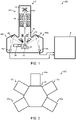
FIG. 1 and FIG. 2 are diagrams illustrating a configuration of theanalyzer 100 according to an embodiment of the invention. Theanalyzer 100 is an EPMA equipped with wavelength dispersive X-ray spectrometers (WDSs). Theanalyzer 100 may be a scanning electron microscope equipped with WDSs. - As illustrated in
FIG. 1 , theanalyzer 100 includes an analyzermain body 2 and animage processor 4. The analyzermain body 2 includes an electronoptical system 10, aspecimen stage 20, anelectron detector 30, aWDS 50a, aWDS 50b, aWDS 50c, aWDS 50d, and aWDS 50e. InFIG. 2 , only the electronoptical system 10 and five WDSs are illustrated for convenience. - The analyzer
main body 2 measures a specimen S. By the analyzermain body 2 measuring the specimen S, an electron image and an X-ray image can be acquired. The electron image is an image acquired by detecting electrons emitted from the specimen S, and is a back-scattered electron image or a secondary electron image, for example. The X-ray image is an image acquired by detecting an X-ray emitted from the specimen S, and is an X-ray map (element distribution map), for example. - The electron
optical system 10 forms an electron probe constituted of focused electron beam EB. The electronoptical system 10 includes anelectron gun 12, a focusinglens 14, adeflector 16 and anobjective lens 18. - The
electron gun 12 generates an electron beam EB. Theelectron gun 12 emits the electron beam EB, which was accelerated by a predetermined accelerating voltage, toward the specimen S. - The focusing
lens 14 is a lens to focus the electron beam EB emitted from theelectron gun 12. Thedeflector 16 deflects the electron beam EB two-dimensionally. By deflecting the electron beam EB using thedeflector 16, the specimen S can be scanned with the electron probe. Theobjective lens 18 is a lens for focusing the electron beam EB on the specimen S. The electron probe can be formed by focusing the electron beam EB using the focusinglens 14 and theobjective lens 18. - The
specimen stage 20 supports the specimen S. The specimen S is placed on thespecimen stage 20. Thespecimen stage 20 includes a moving mechanism (not illustrated) to move the specimen S. By moving the specimen S on thespecimen stage 20, the position on the specimen S to which the electron beam EB is applied, can be changed. - In the
analyzer 100, the specimen S may be scanned with the electron probe by deflecting the electron beam EB using thedeflector 16, or the specimen S may be scanned with the electron probe by moving the specimen S on thespecimen stage 20. - The
electron detector 30 is a detector for detecting electrons emitted from the specimen S. An electron image can be acquired by detecting the electrons emitted from the specimen S using theelectron detector 30. Theelectron detector 30 may be a back-scattered electron detector that detects back-scattered electrons, or a secondary electron detector that detects secondary electrons. In other words, the electron image may be either a back-scattered electron image or a secondary electron image. - The
WDS 50a includes a spectroscopic element (spectroscopic crystal) 52 and anX-ray detector 54. In theWDS 50a, a characteristic X-ray generated from the specimen S is spectrally dispersed by thespectroscopic element 52, and the spectrally dispersed X-ray is detected by theX-ray detector 54. - The
spectroscopic element 52 is a spectroscopic crystal for spectrally dispersing light using the diffraction phenomenon of X-rays. TheWDS 50a includes a plurality ofspectroscopic elements 52 of which crystal plane inter-values are mutually different. In other words, the plurality ofspectroscopic elements 52 have mutually different spectroscopic wavelength ranges. Thespectroscopic elements 52, PET, LiF, TAP, LDE or the like, may be used. TheX-ray detector 54 detects a characteristic X-ray spectrally dispersed by thespectroscopic element 52. - As illustrated in
FIG. 2 , the analyzermain body 2 includes theWDS 50a,WDS 50b,WDS 50c,WDS 50d andWDS 50e. Each of these five WDSs includes a plurality ofspectroscopic elements 52 and theX-ray detector 54. Thereby theanalyzer 100 can perform the WDS analysis in a wide spectroscopic wavelength range. Further, the five WDSs can simultaneously detect X-rays having mutually different energies, therefore five X-ray maps can be acquired simultaneously. - The X-ray map (element distribution map) is generated by measuring the intensity of an X-ray unique to each element, while scanning the specimen S with the electron probe, and visualizing the difference of the intensity of the X-ray (counting rate) at each measurement point on the specimen S.
- A number of WDSs included in the analyzer
main body 2 is not especially limited. - In the analyzer
main body 2, the electronoptical system 10 forms the electron probe, and the specimen S is scanned with this electron probe. By scanning the specimen S with the electron probe, secondary electrons, back-scattered electrons, X-rays (characteristic X-rays) and the like are emitted from each measurement point of the specimen S. An electron image can be acquired by detecting the electrons emitted from each measurement point using theelectron detector 30, and generating an image of the distribution of the intensity of the electrons. Further, an X-ray map can be acquired by detecting the X-ray emitted from each measurement point using theWDS 50a,WDS 50b,WDS 50c,WDS 50d andWDS 50e, and generating an image of the distribution of the X-ray. -
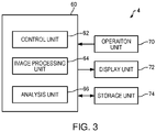
FIG. 3 is a block diagram illustrating a configuration of theimage processor 4. - The
image processor 4 processes an image based on the result of the measurement of the specimen S performed by the analyzermain body 2. As indicated inFIG. 3 , theimage processor 4 includes aprocessing unit 60, anoperation unit 70, adisplay unit 72 and astorage unit 74. - The
operation unit 70 acquires operation signals in accordance with the operation performed by the user, and sends the operation signals to theprocessing unit 60. Theoperation unit 70 consists of: buttons, keys, a touch panel type display, a microphone, or the like. - The
display unit 72 displays an image generated by theprocessing unit 60. Thedisplay unit 72 is implemented by such a display as a liquid crystal display (LCD), for example. - The
storage unit 74 stores programs and data for theprocessing unit 60 to perform various computing processing and image processing. Thestorage unit 74 is also used as a work area of theprocessing unit 60. Thestorage unit 74 is implemented by a random access memory (RAM), a read only memory (ROM), a hard disk and the like, for example. - The
processing unit 60 performs processing of correcting the positional deviation of an image, processing of generating a phase map from a plurality of X-ray maps, and the like. The functions of theprocessing unit 60 are implemented by various processors (e.g. central processing unit (CPU)) executing programs stored in thestorage unit 74. Theprocessing unit 60 includes acontrol unit 62, animage processing unit 64 and ananalysis unit 66. - The
control unit 62 controls the analyzermain body 2. For example, thecontrol unit 62 causes the analyzermain body 2 to perform the measurement to acquire an electron image and the measurement to acquire the X-ray map. - The
image processing unit 64 acquires the electron image and the X-ray map based on the result of the measurement by the analyzermain body 2, and performs image processing on the electron image and the X-ray image. For example, theimage processing unit 64 performs processing of correcting the positional deviations of a plurality of X-ray maps acquired by a plurality of times of measurement. - The
analysis unit 66 analyzes the correlations among the elements based on the plurality of X-ray maps of which positional deviation was corrected by theimage processing unit 64, and creates the phase map. - The
analyzer 100 can create a phase map. In order to create a phase map, a plurality of X-ray maps must be acquired in a same measurement target region. Theanalyzer 100 is equipped with the five WDSs, hence five X-ray maps can be acquired simultaneously. If six or more X-ray maps are acquired in a same measurement region of the specimen S, the same region must be measured a plurality of times. In this case, a positional deviation may be generated among the X-ray maps for such a reason as specimen drift. - The
analyzer 100 can correct the positional deviation among the X-ray maps acquired by performing the measurement for a plurality of times in the same measurement target region. Image processing to correct the positional deviation of the X-ray maps will be described next. -
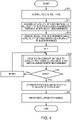
FIG. 4 is a flow chart illustrating an example of the image processing. - First the
image processing unit 64 acquires a reference image, which is an electron image to be a reference to correct the positional deviation (S10). - For example, the
control unit 62 causes the analyzermain body 2 to measure the measurement target region of the specimen S, and theimage processing unit 64 acquires a measurement image, which is an electron image based on this measurement result. - Then the
control unit 62 causes the analyzermain body 2 to measure the measurement target region of the specimen S for a plurality of times, and theimage processing unit 64 acquires a plurality of X-ray maps and a plurality of electron images (measurement images) (S12). - The analyzer
main body 2 includes five WDSs, which means that five X-ray maps can be acquired in one measurement step. Further, the analyzermain body 2 includes theelectron detector 30, hence an electron image can be acquired simultaneously with the X-ray maps. In this description, it is assumed that the specimen S is measured for N times (N > 2), and five X-ray maps and one electron image are acquired in one measurement step. In other words, theimage processing unit 64 acquires 5 × N number of X-ray maps and N number of electron images. - For example, the
control unit 62 causes the analyzermain body 2 to measure the measurement target region of the specimen S for N times, and theimage processing unit 64 acquires 5 × N number of X-ray maps and N number of electron images based on these measurement results. - Then the
image processing unit 64 increases the resolution of the acquired reference image, the 5 × N number of X-ray maps and the N number of electron images (S14). - The resolution is increased by interpolating the pixels of the image, for example. The method of increasing the resolution is not especially limited.
- Then the
image processing unit 64 creates a first correction table T1 for correcting the positional deviations of the five X-ray maps acquired in the first (M = 1) measurement (S16). - The first correction table T1 is a table in which, for each pixel of the X-ray map, a positional deviation amount of the pixel in the X direction and a positional deviation amount of the pixel in the Y direction are registered. The first correction table T1 is a table created by calculating the positional deviation amount between the reference image and the electron image acquired in the first measurement. The processing to create the first correction table T1 will be described later.
- Then the
image processing unit 64 determines whether M = N is established (S18). In other words, theimage processing unit 64 determines whether the Nth correction table TN for correcting the positional deviations of the five X-ray maps acquired in the Nth measurement is created. - If it is determined that M = N is not established (No in S18), processing returns to the processing S16, and the
image processing unit 64 creates a second correction table T2 for correcting the positional deviations of the five X-ray maps acquired in the second (M = 2) measurement (S16). - The
image processing unit 64 repeats the processing S16 until M = N is determined in the processing S18, that is, until the Nth correction table TN is created. - If it is determined that M = N is established (Yes in S18), the
image processing unit 64 corrects the positional deviations of the 5 × N number of X-ray maps using from the first to Nth correction tables T1 to TN (S20). - For example, using the first correction table T1, the
image processing unit 64 corrects the positional deviations of the five X-ray maps acquired in the first measurement. In the same manner, using the second correction table T2, theimage processing unit 64 corrects the positional deviations of the five X-ray maps acquired in the second measurement. In the same manner, using the Nth correction table TN, theimage processing unit 64 corrects the positional deviations of the five X-ray maps acquired in the Nth measurement. - For each of the corrected 5 × N number of X-ray maps, the
image processing unit 64 may perform processing to crop both ends of an image by a number of pixels corresponding to the maximum deviation amount. This allows the 5 × N number of X-ray maps to be in the same field-of-view. - The
image processing unit 64 returns the resolution of the 5 × N number of X-ray maps, which was enhanced in the processing S14, to the original resolution (S22). The method of returning the resolution of the X-ray maps to the original resolution is not especially limited. Then theimage processing unit 64 ends the image processing. - By the above processing, the positional deviations of the 5 × N number of X-ray maps can be corrected.
-
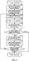
FIG. 5 is a flow chart illustrating an example of the processing S16 of creating the correction table. - The
image processing unit 64 calculates the positional deviation amount of an electron image acquired in the first (M = 1) measurement (hereafter referred to as "first electron image") (S100). - The
image processing unit 64 calculates a positional deviation amount of the first electron image from the reference image. The positional deviation amount is calculated by performing pattern matching between all the regions of the reference image and all the regions of the first electron image, for example. The positional deviation amount is expressed by the positional deviation amount of the electron image in the X direction, and the positional deviation amount of the electron image in the Y direction. - The
image processing unit 64 registers the positional deviation amount, which was calculated in the processing step S100, in the first correction table T1 (S102). The first correction table T1 is stored in thestorage unit 74, for example. -
FIG. 6 is a diagram for describing the first correction table T1. - As indicated in
FIG. 6 , in the first correction table T1, coordinates (X, Y) of each pixel of the first electron image and the positional deviation amount of each pixel are linked and registered. The first correction table T1 includes a table to indicate the positional deviation amount of each pixel in the X direction, and a table to indicate the positional deviation amount of each pixel in the Y direction. The tables inFIG. 6 indicate the positional deviation amounts of each pixel in the X direction. - The positional deviation amounts are calculated by pattern matching all the regions of the reference image and all the regions of the first electron image, hence a same value is registered for all the pixels in the first correction table T1. A positional deviation in one direction can be corrected using this first correction table T1.
- Then the
image processing unit 64 corrects the positional deviation of the first electron image using the first correction table T1 (S104). - Then the
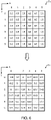
image processing unit 64 divides the first electron image and the reference image into a plurality of partial images respectively (S106). -
FIG. 7 is a diagram for describing the processing of dividing the first electron image E1. As indicated inFIG. 7 , the first electron image E1 is divided into four partial image EPs (an example of partial measurement images). A partial image EP is an image acquired by equally dividing the field-of-view of the first electron image E1, for example. In the case of the example inFIG. 7 , the first electron image E1 is divided into two in the X direction and into two in the Y direction, whereby four partial image EPs are created. Just like the first electron image E1, the reference image R is also divided into four partial image RPs (an example of partial reference images). A partial image RP is an image acquired by equally dividing the field-of-view of the reference image R. - The dividing processing in S106 will be described in detail later in "2.1.4. Processing of dividing electron image".
- In each of the four partial image EPs, the
image processing unit 64 calculates the positional deviation amount relative to the corresponding partial image RP (S108). - For example, the
image processing unit 64 performs pattern matching between one partial image EP and a partial image RP corresponding to this one partial image EP, then calculates the positional deviation amount of a center pixel O of this one partial image EP from the center of the partial image RP. Theimage processing unit 64 performs this calculation of the positional deviation amount of the center pixel O for the four partial image EPs respectively. The center pixel O is a pixel matching with or closest to the center of the partial image. - The
image processing unit 64 determines whether the positional deviation amounts of the center pixels O of the four partial image EPs are a threshold or less (S110). - The
image processing unit 64 determines whether the positional deviation amounts are not the threshold or less if at least one of the positional deviation amounts of the center pixels O of the four partial image EPs exceeds the threshold. The threshold is set to an arbitrary value. As the threshold becomes smaller, the positional deviation can be corrected more accurately. - If it is determined that the positional deviation amounts are not the threshold or less (No in S110), the
image processing unit 64 calculates the positional deviation amounts of all the pixels of the first electron image E1 (S112). -
FIG. 8 is a diagram for describing the processing of calculating the positional deviation amounts of all the pixels of the first electron image E1. - The positional deviation amounts of all the pixels of the first electron image E1 are calculated based on the positional deviation amounts of the center pixels O of the adjacent partial image EPs. For example, as indicated in
FIG. 8 , the positional deviation amounts of the other pixels are interpolated from the positional deviation amounts of the center pixels O of the partial image EPs. In the case of the example inFIG. 8 , the positional deviations of the pixels disposed in the X direction are linearly interpolated first, using the positional deviation amounts of the center pixels O disposed in the X direction. Then the positional deviation amounts of the pixels disposed in the Y direction are linearly interpolated using the positional deviation amounts of the center pixels O disposed in the Y direction. Finally, the positional deviation amounts of the remaining pixels are interpolated using the positional deviation amounts of the adjacent pixels. Thereby the positional deviation amounts of all the pixels of the first electron image E1 can be calculated. The method of calculating the positional deviation amounts of each pixel is not especially limited. - The
image processing unit 64 registers the calculated positional deviation amounts of all the pixels of the first electron image E1 in the first correction table T1, and updates the first correction table T1 (S114). - As indicated in
FIG. 6 , in the processing step S100, the positional deviation amounts are calculated by pattern matching between all the regions of the reference image R and all the regions of the first electron image E1, hence in the processing S102, the same values are registered in the first correction table T1 as the positional deviation amounts of all the pixels. In the first correction table T1, the positional deviation in one direction can be corrected. - In the
processing S1 12, the positional deviation amounts of all the pixels are calculated based on the positional deviation amount determined for each partial image EP. Therefore in the first correction table T1 updated in the processing S114, not only the positional deviation in one direction, but also the enlargement/reduction, distortion and the like can be corrected. - The
image processing unit 64 determines whether the processing S104, the processing S106, the processing S108, the processing S110, the processing S112 and the processing S 114 were repeated for a predetermined number of times (S116). The predetermined number of times can be set to an arbitrary number. - If it is determined that the above processing steps were not repeated for a predetermined number of times (No in S116), the
image processing unit 64 returns to the processing S104, and corrects the positional deviation of the first electron image E1 using the first correction table T1. Then theimage processing unit 64 performs the processing of dividing the electron image (S106), the processing of calculating the positional deviation amount of each partial image (S108), the processing of determining whether the positional deviation amount is the threshold or less (S110), the processing of calculating the positional deviation amounts of all the pixels (S112), and the processing of registering the positional deviation amounts (S114). - The
image processing unit 64 repeats the processing S104, the processing S106, the processing S108, the processing S110, the processing S112 and the processing S114 until it is determined that the above processing steps were repeated for a predetermined number of times in the processing S 116 (Yes in S116), or it is determined that the positional deviation amount is the threshold or less (Yes in S110). - The
image processing unit 64 ends the processing of creating the first correction table T1 if it is determined that the above processing steps were repeated for a predetermined number of times in the processing S 116 (Yes in S116), or it is determined that the positional deviation amount is the threshold or less in the processing S110 (Yes in S 110). - The above describes the processing of creating the first correction table T1, but the same description is also applicable to each processing of creating from the second to the Nth correction tables T2 to TN.
-
FIG. 9 is a diagram for describing the processing S 106 of dividing the electron image. - As indicated in
FIG. 9 , a number of the partial image EPs can be increased by repeating the processing of dividing the first electron image E1 so as to decrease the size of the partial image EP, that is, to decrease the area (number of pixels) of the partial image EP, and thereby the positional deviation of the first electron image E1 can be corrected more accurately. However, as the size of the partial image EP decreases, the accuracy of pattern matching also decreases. - Hence in the case where the size of the partial image EP becomes a predetermined reference size or less, the
image processing unit 64 increases a number of partial image EPs by increasing the overlapping amounts of the adjacent partial image EPs, without changing the size of the partial image EP. -
FIG. 10 is a diagram for describing the processing of increasing the overlapping amount of the adjacent partial image EPs. - As indicated in
FIG. 10 , a number of partial image EPs can be increased without changing the size of the partial image EP, by increasing the overlapping amount of the adjacent partial image EPs. InFIG. 10 , the overlapping amount of the partial image EPs which are adjacent in the X direction is increased. However, the overlapping amount of the partial image EPs which are adjacent in the Y direction may be increased, or both the overlapping amount of the partial image EPs which are adjacent in the X direction and the overlapping amount of the partial image EPs which are adjacent in the Y direction may be increased. -
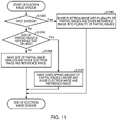
FIG. 11 is a flow chart illustrating an example of the processing of dividing the electron image. - The
image processing unit 64 determines whether the processing of dividing the first electron image E1 is the first time (S1060), and if it is determined that the processing is the first time (Yes in S1060), theimage processing unit 64 divides the first electron image E1 into a plurality of partial image EPs, as indicated inFIG. 7 (S 1062). Theimage processing unit 64 also divides the reference image R into a plurality of partial image RP in the same manner as the first electron image E1. - If it is determined that the processing of dividing the first electron image E1 is not the first time (No in S1060), the
image processing unit 64 determines whether the size of the partial image (partial image EP and partial image RP) is a reference size or less (S1064). The reference size is set to a minimum size with which pattern matching can be performed accurately, for example. The reference size, however, can be set arbitrarily, in accordance with the required accuracy of pattern matching, the repeat cycle of the patterns, and the like. - If it is determined that the size of the partial image is not the reference size or less (No in S 1064), the
image processing unit 64 decreases the size of the partial image, with which the first electron image E1 and the reference image R are divided, as indicated inFIG. 9 (S 1068). For example, theimage processing unit 64 decreases the size of the partial image in the Mth processing S1068 to be smaller than the size of the partial image in the M-lth processing S 1068. Thereby a number of partial images generated in the Mth processing S1068 becomes more than the number of partial images generated in the M-lth processing S1068. - If it is determined that the size of the partial image is the reference size or less (Yes in S 1064), the
image processing unit 64 makes the overlapping amount of the adjacent partial image EPs to be larger without changing the size of the partial image EPs, as indicated inFIG. 10 , and thereby divides the first electron image E1 and the reference image R (S 1070). For example, theimage processing unit 64 makes the overlapping amount of the adjacent partial images in the Mth processing S1070 to be larger than the overlapping amount of the adjacent partial images in the M-lth processing S 1070. Thereby a number of partial images generated in the Mth processing S1070 becomes more than the number of partial images generated in the M-lth processing S1070. - After the processing S 1062, the processing S1068 or the processing S1070 is performed to divide the first electron image E1 and the reference image R, the
image processing unit 64 ends the processing S106 of dividing the electron image. - The above describes the processing of dividing the first electron image E1, but the same description is also applicable to each processing of dividing the second to the Nth electron images.
- In the
analyzer 100, theanalysis unit 66 creates a phase map using 5 × N number of X-ray maps of which positional deviations have been corrected in the above image processing. - The
analysis unit 66 creates scatter plots based on the 5 × N number of X-ray maps. For example, two maps are selected from the 5 × N number of X-ray maps, and plots the X-ray intensity of each pixel in the scatter plots, of which the ordinate is the X-ray intensity of one of the selected two maps, and the abscissa is the X-ray intensity of the other thereof.FIG. 12 indicates the scatter plots. - Then the
analysis unit 66 searches the unevenly distributed areas in the scatter plots, encloses the unevenly distributed areas, and color code those areas. By showing colors on the display of the X-ray map, theanalysis unit 66 creates a phase map.FIG. 13 indicates the phase map. - In the
analyzer 100, theimage processing unit 64 divides the measurement image, which is an electron image of which positional deviation is corrected, and the reference image, which is an electron image to be a reference of the positional deviation correction, into partial images respectively, and in each of the plurality of partial images generated by dividing the measurement image, a positional deviation amount from a corresponding partial image of the reference image is calculated, and the positional deviation of the measurement image is corrected based on this positional deviation amount. Therefore in theanalyzer 100, not only the positional deviation in one direction, but the enlargement/reduction, distortion and the like can also be corrected. As described above, in theanalyzer 100, the positional deviation between the measurement image and the reference image, acquired at different timings, can be accurately measured. - In the
analyzer 100, the size of the partial image in the dividing processing S1068 for the Mth time is made smaller than the size of the partial image in the dividing processing S1068 for the M-lth time. Since theanalyzer 100 gradually decreases the size of the partial image like this, a drop in the accuracy of the pattern matching, when the positional deviation amount is calculated, can be minimized. For example, in a case where there are many similar patterns in a measurement image, if the size of the partial image changes considerably, then pattern recognition errors tend to occur, and the accuracy of the pattern matching drops. - In the
analyzer 100, in a case where it is determined that the size of the partial image EP is the reference size or less, an overlapping amount of the adjacent partial images is increased when the measurement image and the reference image are divided. In other words, in the dividing processing S1070 for the Mth time, the overlapping amount of the adjacent partial images is increased compared with the dividing processing S1070 for the M-lth time. Thereby a drop in the accuracy of the pattern matching caused by a decrease in the size of the partial image can be minimized. - In the
analyzer 100, theimage processing unit 64 creates a correction table for correcting the positional deviation of the measurement image, based on the positional deviation amount of a plurality of partial images acquired by dividing the measurement image. Therefore using the correction table, theanalyzer 100 can correct the positional deviation of the X-ray map, which is acquired simultaneously with the measurement image. - Here the back-scattered electrons and the secondary electrons have high signal amounts compared with the characteristic X-rays. Therefore the positional deviation of the X-ray map can be corrected more accurately by calculating the positional deviation amount using the electron image to create the correction table, and correcting the X-ray map using this correction table. In particular, even in the case of the X-ray map of a trace element of which S/N ratio is insufficient, the positional deviation of the X-ray map can be accurately corrected.
- For example, in order to analyze the correlation of the element A and the element B, in a case where the positional deviation of the X-ray map cannot be corrected, an X-ray map, indicating a distribution of an element A and an X-ray map indicating a distribution of an element B must be measured simultaneously. Furthermore, in order to analyze the correlations among multiple elements, the measurement must be repeated with changing the combination of the measurement target element.
-
FIG. 14 is a diagram illustrating a positional deviation between an X-ray map based on the first measurement (1seq) and an X-ray map based on the second measurement (2seq). InFIG. 14 , the distribution of the intensity of the X-ray of Cr and the distribution of the intensity of the X-ray of C are indicated. - As indicated in
FIG. 14 , the X-ray map acquired in the second measurement has a positional deviation from the X-ray map acquired in the first measurement. -
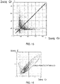
FIG. 15 is a scatter plot of the intensity of each pixel of the X-ray map of Cr based on the first measurement and the intensity of each pixel of the X-ray map of Cr based on the second measurement. InFIG. 15 , the abscissa indicates the intensity of the X-ray of the Cr in the first measurement, and the ordinate indicates the intensity of the X-ray of the Cr in the second measurement. - In a case where the X-ray map acquired in the second measurement has no positional deviation from the X-ray map acquired in the first measurement, the data is distributed on the line indicated in
FIG. 15 . In a case where the X-ray map acquired in the second measurement has positional deviation from the X-ray map acquired in the first measurement as indicated inFIG. 14 , the data is not distributed on the line indicated inFIG. 15 . -
FIG. 16 is a scatter plot of the intensity of each pixel of the X-ray map of C and the intensity of each pixel of the X-ray map of Cr, which were measured simultaneously.FIG. 17 is a scatter plot of the intensity of each pixel of the X-ray map of C and the intensity of each pixel of the X-ray map of Cr, in a case where positional deviation exists. - As indicated in
FIG. 16 , in the case where there is no positional deviation, the correlations of Cr and C are correctly indicated on the scatter plot. In the case where a positional deviation exists, on the other hand, the correlation of Cr and C is not correctly indicated in the scatter plot. Therefore the elements, to be the targets of the correlation analysis, must be measured simultaneously. -
FIG. 18 is a table indicating an example of the combinations of the measurement elements in a case where the correlations of an element A, element B, element C, element D, element E and element F are analyzed. - As indicated in
FIG. 18 , in order to analyze the correlations among multiple elements, the measurement must be repeated many time while changing the measurement elements gradually, so that all combinations of the target elements of the correlation analysis can be measured simultaneously. - However, in the case of the
analyzer 100, the positional deviations of the X-ray maps acquired at different timings can be corrected, hence there is no need to measure the same element many times. Therefor in theanalyzer 100, the measurement time can be decreased even in the case of analyzing the correlations among multiple elements. -
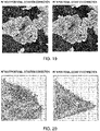
FIG. 19 indicates images generated by superimposing two back-scattered electron images acquired at different timings. As indicated inFIG. 19 , the two back-scattered electron images are accurately superimposed by correcting the positional deviation between the two back-scattered electron images. - In the
analyzer 100, the positional deviation of the X-ray maps acquired at different timings can be corrected, hence even in a case of creating a phase map which indicates the distribution of compounds, an accurate phase map can be created in a short time. -
FIG. 20 indicates the scatter plots of the intensity of each pixel of two X-ray maps acquired at different timings. As indicated inFIG. 20 , the correlation of the two elements can be accurately indicated by correcting the potential deviations of the two X-ray maps. - The invention is not limited to the above-described embodiments, and various modifications can be made within the scope of the invention.
- In the above embodiment, the target X-ray map of the positional deviation correction and the electron image are acquired after the reference image is acquired, as indicated in
FIG. 4 , but an electron image acquired at the same time with the target X-ray map of the positional deviation correction may be used as the reference image. For example, the electron image acquired in the first measurement may be used as the reference image. -
FIG. 21 is a diagram for describing a modification of the processing of dividing an electron image. - In the above example indicated in
FIG. 9 , the first electron image E1 is divided by 2 in the X direction and is divided by 2 in the Y direction, creating a total of four partial image EPs. Then the first electron image E1 is divided by 3 in the X direction and is divided by 3 in the Y direction, creating a total of nine partial image EPs. Then the first electron image E1 is divided by 6 in the X direction and is divided by 6 in the Y direction, creating a total of 36 partial image EPs. In this way, in the case of the example inFIG. 9 , a number of divisions in the X direction and a number of divisions in the Y direction are the same. Here the X direction is a direction of scanning with an electron probe, and the Y direction is a direction orthogonal to the scanning direction. - In the example indicated in
FIG. 21 , on the other hand, the first electron image E1 is divided by 2 in the Y direction to create two partial image EPs first, then the first electron image E1 is divided by 3 in the Y direction to create three partial image EPs, and then the first electron image E1 is divided by 6 in the Y direction to create six partial image EPs. - In this way, in the case of the example in
FIG. 21 , the first electron image E1 is divided only in the Y direction, and not in the X direction. This is because compared with the Y direction, the influence of specimen drift is quite minor in the X direction, since the X direction is the direction of scanning with an electron probe. - In the case of the example in
FIG. 21 , the first electron image E1 is not divided in the X direction, but may be divided in the X direction by a number smaller than in the Y direction. - In the above embodiment, the positional deviation of the X-ray map is corrected using the positional deviation amount of the electron image, but the target image of the correction is not limited to the X-ray map. For example, the target image of the correction may be a cathode luminescence image, an absorption current image, a secondary electron image, a back-scattered electron image, an Auger electron image, or the like.
- In the above embodiment, the positional deviation of the X-ray map is corrected using the positional deviation amount of the electron image, but the positional deviation amount may be calculated using an image that is acquired by detecting signals of which signal amount is higher than the X-ray, and the positional deviation of the X-ray map may be corrected using this calculated positional deviation amount.
- In the above embodiment, a case where the analyzer is an EPMA was described, but the analyzer according to the invention is not limited to an EPMA. The analyzer according to the invention may be any apparatus that can acquire map data and image data of various signals of electrons, X-rays, and the like. For example, the analyzer according to the invention may be a scanning electron microscope, an Auger electron microscope, or a fluorescence X-ray spectrometer.
- The above-described embodiments and modifications are examples, and the invention is not limited thereto. For example, the embodiments and the modifications may be combined appropriately.
- The invention is not limited to the above-described embodiments, and various modifications can be made. For example, the invention includes configurations that are substantially the same as the configurations described in the embodiments. Substantially same configurations means configurations having the same functions or methods, for example. The invention also includes configurations obtained by replacing non-essential elements described in the embodiments are replaced by other elements. The invention further includes configurations obtained by adding known art to the configurations described in the embodiments.
- Some embodiments of the invention have been described in detail above, but a person skilled in the art will readily appreciate that various modifications can be made from the embodiments without materially departing from the novel teachings and effects of the invention as defined by the claims. Accordingly, all such modifications are assumed to be included in the scope of the invention.
Claims (6)
- An analyzer comprising:an analyzer main body that measures a specimen; andan image processing unit that processes images based on a result of measurement of the specimen,the image processing unit performing processing of:acquiring a reference image which is obtained by measuring an analysis target region of the specimen by the analyzer main body;acquiring a measurement image which is obtained by measuring the analysis target region by the analyzer main body;dividing the measurement image into a plurality of partial measurement images, and dividing the reference image into a plurality of partial reference images;calculating a positional deviation amount of each of the partial measurement images relative to a corresponding partial reference image among the partial reference images;determining whether or not the positional deviation amount is a threshold or less; andcorrecting positional deviation of the measurement image based on the positional deviation amounts of the plurality of partial measurement images when the image processing unit has determined that the positional deviation amount is not the threshold or less,the processing of dividing, the processing of calculating the positional deviation amount, the processing of determining, and the processing of correcting the positional deviation being repeated until the image processing unit determines that the positional deviation amount is the threshold or less, andthe processing of dividing for an Mth time including processing of:determining whether or not a size of each of the partial measurement images in the processing of dividing for an M-lth time is a reference size or less;making a size of each of the partial measurement images in the processing of dividing for the Mth time to be smaller than the size of each of the partial measurement images in the processing of dividing for the M-lth time when the image processing unit has determined that the size of each of the partial measurement images for the M-lth time is not the reference size or less; andmaking an overlapping amount of adjacent partial measurement images among the plurality of partial measurement images to be larger than the overlapping amount in the processing of dividing for the M-lth time when the image processing unit has determined that the size of each of the partial measurement images for the M-lth time is the reference size or less.
- The analyzer according to claim 1, wherein
the image processing unit performs processing of creating a correction table which is used for correcting the positional deviation of the measurement image based on the positional deviation amounts of the plurality of partial measurement images. - The analyzer according to claim 2, wherein
the analyzer main body includes:an electron optical system that illuminates the specimen with an electron beam;an electron detector that detects electrons emitted from the specimen illuminated with an electron beam; andan X-ray detector that detects an X-ray emitted from the specimen illuminated with an electron beam,the reference image and the measurement image are electron images acquired by detecting electrons by the electron detector,the analyzer main body acquires an X-ray image acquired by detecting an X-ray by the X-ray detector simultaneously with the electron images, andthe image processing unit uses the correction table to perform processing of correcting positional deviation of the X-ray image acquired simultaneously with the measurement image. - The analyzer according to any one of claims 1 to 3, wherein
the processing of calculating the positional deviation amount includes processing of:calculating, in each of the plurality of partial measurement images, a positional deviation amount of a center of each of the partial measurement image from a center of the corresponding partial reference image; andcalculating, positional deviation amounts of a plurality of pixels constituting the adjacent partial measurement images based on positional deviation amounts of centers of the adjacent partial measurement images. - The analyzer according to any one of claims 1 to 4, wherein
the measurement image is an image generated by scanning the specimen with an electron beam, detecting electrons emitted from each measurement point, and imaging a distribution of electron intensity. - An image processing method comprising steps of:acquiring a reference image by measuring an analysis target region of a specimen by using an analyzer;acquiring a measurement image by measuring the analysis target region by using the analyzer;dividing the measurement image into a plurality of partial measurement images, and dividing the reference image into a plurality of partial reference images;calculating a positional deviation amount of each of the partial measurement images relative to a corresponding partial reference image among the partial reference images;determining whether or not the positional deviation amount is a threshold or less; andcorrecting positional deviation of the measurement image based on the positional deviation amounts of the plurality of partial measurement images when it has been determined that the positional deviation amount is not the threshold or less,the step of dividing, the step of calculating the positional deviation amount, the step of determining, and the step of correcting the positional deviation being repeated until it is determined that the positional deviation amount is the threshold or less, andthe step of dividing for an Mth time including:determining whether or not a size of each of the partial measurement images in the step of dividing for an M-lth time is a reference size or less;making a size of each of the partial measurement images in the step of dividing for the Mth time to be smaller than the size of each of the partial measurement images in the step of dividing for the M-lth time when it has been determined that the size of each of the partial measurement images is not the reference size or less; andmaking an overlapping amount of adjacent partial measurement images among the partial measurement images to be larger than the overlapping amount in the step of dividing for the M-lth time when it has been determined that the size of each of the partial measurement images is the reference size or less.
Applications Claiming Priority (1)
| Application Number | Priority Date | Filing Date | Title |
|---|---|---|---|
| JP2021016519A JP7250054B2 (en) | 2021-02-04 | 2021-02-04 | Analysis device and image processing method |
Publications (2)
| Publication Number | Publication Date |
|---|---|
| EP4040144A1 true EP4040144A1 (en) | 2022-08-10 |
| EP4040144B1 EP4040144B1 (en) | 2024-04-03 |
Family
ID=80225927
Family Applications (1)
| Application Number | Title | Priority Date | Filing Date |
|---|---|---|---|
| EP22154930.6A Active EP4040144B1 (en) | 2021-02-04 | 2022-02-03 | Analyzer and image processing method |
Country Status (3)
| Country | Link |
|---|---|
| US (1) | US11733188B2 (en) |
| EP (1) | EP4040144B1 (en) |
| JP (1) | JP7250054B2 (en) |
Families Citing this family (1)
| Publication number | Priority date | Publication date | Assignee | Title |
|---|---|---|---|---|
| TWI911779B (en) * | 2023-07-21 | 2026-01-11 | 德商卡爾蔡司Smt有限公司 | Methods of three-dimensional (3d) volume image acquisition and dual beam systems |
Citations (2)
| Publication number | Priority date | Publication date | Assignee | Title |
|---|---|---|---|---|
| US20120181425A1 (en) * | 2011-01-17 | 2012-07-19 | Jeol Ltd. | Electron Probe Microanalyzer and Data Processing Method Implemented Therein |
| US20190122913A1 (en) * | 2017-10-20 | 2019-04-25 | Kla-Tencor Corporation | Multi-step image alignment method for large offset die-die inspection |
Family Cites Families (8)
| Publication number | Priority date | Publication date | Assignee | Title |
|---|---|---|---|---|
| JP3454052B2 (en) * | 1996-12-05 | 2003-10-06 | 株式会社日立製作所 | Electron beam analyzer |
| JP2000106121A (en) * | 1998-07-29 | 2000-04-11 | Jeol Ltd | Electron microscope or similar device |
| JP5069904B2 (en) * | 2006-03-28 | 2012-11-07 | 株式会社日立ハイテクノロジーズ | Designated position specifying method and designated position measuring device |
| JP5086818B2 (en) * | 2008-01-16 | 2012-11-28 | 株式会社日立ハイテクノロジーズ | Electron microscope equipment |
| JP2013201530A (en) * | 2012-03-23 | 2013-10-03 | Canon Inc | Imaging device and control method of the same |
| JP6468160B2 (en) * | 2015-10-16 | 2019-02-13 | 株式会社島津製作所 | Scanning charged particle microscope |
| JP6565601B2 (en) * | 2015-10-29 | 2019-08-28 | 株式会社島津製作所 | Image correction device |
| JP6859944B2 (en) * | 2017-12-25 | 2021-04-14 | 株式会社島津製作所 | Scanning electron microscope and control program |
-
2021
- 2021-02-04 JP JP2021016519A patent/JP7250054B2/en active Active
-
2022
- 2022-02-03 EP EP22154930.6A patent/EP4040144B1/en active Active
- 2022-02-03 US US17/591,803 patent/US11733188B2/en active Active
Patent Citations (3)
| Publication number | Priority date | Publication date | Assignee | Title |
|---|---|---|---|---|
| US20120181425A1 (en) * | 2011-01-17 | 2012-07-19 | Jeol Ltd. | Electron Probe Microanalyzer and Data Processing Method Implemented Therein |
| JP2012149910A (en) | 2011-01-17 | 2012-08-09 | Jeol Ltd | Data processing method in electronic probe microanalyzer and electronic probe microanalyzer |
| US20190122913A1 (en) * | 2017-10-20 | 2019-04-25 | Kla-Tencor Corporation | Multi-step image alignment method for large offset die-die inspection |
Non-Patent Citations (1)
| Title |
|---|
| OPHUS COLIN ET AL: "Correcting nonlinear drift distortion of scanning probe and scanning transmission electron microscopies from image pairs with orthogonal scan directions", ULTRAMICROSCOPY, ELSEVIER, AMSTERDAM, NL, vol. 162, 10 December 2015 (2015-12-10), pages 1 - 9, XP029410772, ISSN: 0304-3991, DOI: 10.1016/J.ULTRAMIC.2015.12.002 * |
Also Published As
| Publication number | Publication date |
|---|---|
| JP7250054B2 (en) | 2023-03-31 |
| US20220244202A1 (en) | 2022-08-04 |
| EP4040144B1 (en) | 2024-04-03 |
| US11733188B2 (en) | 2023-08-22 |
| JP2022119426A (en) | 2022-08-17 |
Similar Documents
| Publication | Publication Date | Title |
|---|---|---|
| US7372029B2 (en) | Scanning transmission electron microscope and scanning transmission electron microscopy | |
| EP2256780B1 (en) | Transmission electron microscope with electronic spectroscope and method of displaying spectral image | |
| US11435303B2 (en) | X-ray analysis device and peak search method | |
| US6794648B2 (en) | Ultimate analyzer, scanning transmission electron microscope and ultimate analysis method | |
| US7872232B2 (en) | Electronic microscope apparatus | |
| EP4040144B1 (en) | Analyzer and image processing method | |
| US11062434B2 (en) | Method of generating elemental map and surface analyzer | |
| CN114609171B (en) | Surface analysis device | |
| US8450685B2 (en) | Electron probe microanalyzer and data processing method implemented therein | |
| US9627175B2 (en) | Electron microscope and elemental mapping image generation method | |
| US20030085350A1 (en) | Ultimate analyzer, scanning transmission electron microscope and ultimate analysis method | |
| US12249499B2 (en) | Imaging mass spectrometer | |
| US12431326B2 (en) | Charged particle beam device and image acquisition method | |
| US7078688B2 (en) | Shape measuring device and shape measuring method | |
| US12429442B2 (en) | Scanning electron microscope and map display method for absorption edge structure | |
| US11391682B2 (en) | Auger electron microscope and analysis method | |
| JP2023068469A (en) | PHASE ANALYZER, SAMPLE ANALYZER, AND ANALYSIS METHOD | |
| EP4365580A1 (en) | Wavelength-dispersive x-ray spectrometer analyzing method and analyzer | |
| US12631578B2 (en) | Analyzing method and analyzer | |
| JP2002310957A (en) | X-ray analyzer by electronic excitation | |
| KR20200091335A (en) | Microscope and method for calculating depth of 3d structure | |
| US20260002895A1 (en) | Evaluation Method and Analyzer Apparatus | |
| CN112051289A (en) | X-ray analysis apparatus and peak search method | |
| JP2003022774A (en) | Transmission electron microscope | |
| JP2000002674A (en) | Electronic probe micro analyzer |
Legal Events
| Date | Code | Title | Description |
|---|---|---|---|
| PUAI | Public reference made under article 153(3) epc to a published international application that has entered the european phase |
Free format text: ORIGINAL CODE: 0009012 |
|
| STAA | Information on the status of an ep patent application or granted ep patent |
Free format text: STATUS: THE APPLICATION HAS BEEN PUBLISHED |
|
| AK | Designated contracting states |
Kind code of ref document: A1 Designated state(s): AL AT BE BG CH CY CZ DE DK EE ES FI FR GB GR HR HU IE IS IT LI LT LU LV MC MK MT NL NO PL PT RO RS SE SI SK SM TR |
|
| STAA | Information on the status of an ep patent application or granted ep patent |
Free format text: STATUS: REQUEST FOR EXAMINATION WAS MADE |
|
| 17P | Request for examination filed |
Effective date: 20230206 |
|
| RBV | Designated contracting states (corrected) |
Designated state(s): AL AT BE BG CH CY CZ DE DK EE ES FI FR GB GR HR HU IE IS IT LI LT LU LV MC MK MT NL NO PL PT RO RS SE SI SK SM TR |
|
| GRAP | Despatch of communication of intention to grant a patent |
Free format text: ORIGINAL CODE: EPIDOSNIGR1 |
|
| STAA | Information on the status of an ep patent application or granted ep patent |
Free format text: STATUS: GRANT OF PATENT IS INTENDED |
|
| RIC1 | Information provided on ipc code assigned before grant |
Ipc: G06T 7/33 20170101ALI20230825BHEP Ipc: H01J 37/22 20060101ALI20230825BHEP Ipc: G01N 23/2252 20180101AFI20230825BHEP |
|
| INTG | Intention to grant announced |
Effective date: 20230921 |
|
| GRAS | Grant fee paid |
Free format text: ORIGINAL CODE: EPIDOSNIGR3 |
|
| RAP3 | Party data changed (applicant data changed or rights of an application transferred) |
Owner name: JEOL LTD. |
|
| GRAA | (expected) grant |
Free format text: ORIGINAL CODE: 0009210 |
|
| STAA | Information on the status of an ep patent application or granted ep patent |
Free format text: STATUS: THE PATENT HAS BEEN GRANTED |
|
| AK | Designated contracting states |
Kind code of ref document: B1 Designated state(s): AL AT BE BG CH CY CZ DE DK EE ES FI FR GB GR HR HU IE IS IT LI LT LU LV MC MK MT NL NO PL PT RO RS SE SI SK SM TR |
|
| REG | Reference to a national code |
Ref country code: CH Ref legal event code: EP |
|
| REG | Reference to a national code |
Ref country code: IE Ref legal event code: FG4D |
|
| REG | Reference to a national code |
Ref country code: DE Ref legal event code: R096 Ref document number: 602022002597 Country of ref document: DE |
|
| REG | Reference to a national code |
Ref country code: LT Ref legal event code: MG9D |
|
| REG | Reference to a national code |
Ref country code: NL Ref legal event code: MP Effective date: 20240403 |
|
| REG | Reference to a national code |
Ref country code: AT Ref legal event code: MK05 Ref document number: 1672872 Country of ref document: AT Kind code of ref document: T Effective date: 20240403 |
|
| PG25 | Lapsed in a contracting state [announced via postgrant information from national office to epo] |
Ref country code: NL Free format text: LAPSE BECAUSE OF FAILURE TO SUBMIT A TRANSLATION OF THE DESCRIPTION OR TO PAY THE FEE WITHIN THE PRESCRIBED TIME-LIMIT Effective date: 20240403 |
|
| PG25 | Lapsed in a contracting state [announced via postgrant information from national office to epo] |
Ref country code: NL Free format text: LAPSE BECAUSE OF FAILURE TO SUBMIT A TRANSLATION OF THE DESCRIPTION OR TO PAY THE FEE WITHIN THE PRESCRIBED TIME-LIMIT Effective date: 20240403 |
|
| PG25 | Lapsed in a contracting state [announced via postgrant information from national office to epo] |
Ref country code: IS Free format text: LAPSE BECAUSE OF FAILURE TO SUBMIT A TRANSLATION OF THE DESCRIPTION OR TO PAY THE FEE WITHIN THE PRESCRIBED TIME-LIMIT Effective date: 20240803 |
|
| PG25 | Lapsed in a contracting state [announced via postgrant information from national office to epo] |
Ref country code: BG Free format text: LAPSE BECAUSE OF FAILURE TO SUBMIT A TRANSLATION OF THE DESCRIPTION OR TO PAY THE FEE WITHIN THE PRESCRIBED TIME-LIMIT Effective date: 20240403 |
|
| PG25 | Lapsed in a contracting state [announced via postgrant information from national office to epo] |
Ref country code: HR Free format text: LAPSE BECAUSE OF FAILURE TO SUBMIT A TRANSLATION OF THE DESCRIPTION OR TO PAY THE FEE WITHIN THE PRESCRIBED TIME-LIMIT Effective date: 20240403 Ref country code: FI Free format text: LAPSE BECAUSE OF FAILURE TO SUBMIT A TRANSLATION OF THE DESCRIPTION OR TO PAY THE FEE WITHIN THE PRESCRIBED TIME-LIMIT Effective date: 20240403 |
|
| PG25 | Lapsed in a contracting state [announced via postgrant information from national office to epo] |
Ref country code: GR Free format text: LAPSE BECAUSE OF FAILURE TO SUBMIT A TRANSLATION OF THE DESCRIPTION OR TO PAY THE FEE WITHIN THE PRESCRIBED TIME-LIMIT Effective date: 20240704 |
|
| PG25 | Lapsed in a contracting state [announced via postgrant information from national office to epo] |
Ref country code: PT Free format text: LAPSE BECAUSE OF FAILURE TO SUBMIT A TRANSLATION OF THE DESCRIPTION OR TO PAY THE FEE WITHIN THE PRESCRIBED TIME-LIMIT Effective date: 20240805 |
|
| PG25 | Lapsed in a contracting state [announced via postgrant information from national office to epo] |
Ref country code: ES Free format text: LAPSE BECAUSE OF FAILURE TO SUBMIT A TRANSLATION OF THE DESCRIPTION OR TO PAY THE FEE WITHIN THE PRESCRIBED TIME-LIMIT Effective date: 20240403 |
|
| PG25 | Lapsed in a contracting state [announced via postgrant information from national office to epo] |
Ref country code: CZ Free format text: LAPSE BECAUSE OF FAILURE TO SUBMIT A TRANSLATION OF THE DESCRIPTION OR TO PAY THE FEE WITHIN THE PRESCRIBED TIME-LIMIT Effective date: 20240403 |
|
| PG25 | Lapsed in a contracting state [announced via postgrant information from national office to epo] |
Ref country code: AT Free format text: LAPSE BECAUSE OF FAILURE TO SUBMIT A TRANSLATION OF THE DESCRIPTION OR TO PAY THE FEE WITHIN THE PRESCRIBED TIME-LIMIT Effective date: 20240403 |
|
| PG25 | Lapsed in a contracting state [announced via postgrant information from national office to epo] |
Ref country code: PL Free format text: LAPSE BECAUSE OF FAILURE TO SUBMIT A TRANSLATION OF THE DESCRIPTION OR TO PAY THE FEE WITHIN THE PRESCRIBED TIME-LIMIT Effective date: 20240403 |
|
| PG25 | Lapsed in a contracting state [announced via postgrant information from national office to epo] |
Ref country code: LV Free format text: LAPSE BECAUSE OF FAILURE TO SUBMIT A TRANSLATION OF THE DESCRIPTION OR TO PAY THE FEE WITHIN THE PRESCRIBED TIME-LIMIT Effective date: 20240403 |
|
| PG25 | Lapsed in a contracting state [announced via postgrant information from national office to epo] |
Ref country code: PT Free format text: LAPSE BECAUSE OF FAILURE TO SUBMIT A TRANSLATION OF THE DESCRIPTION OR TO PAY THE FEE WITHIN THE PRESCRIBED TIME-LIMIT Effective date: 20240805 Ref country code: PL Free format text: LAPSE BECAUSE OF FAILURE TO SUBMIT A TRANSLATION OF THE DESCRIPTION OR TO PAY THE FEE WITHIN THE PRESCRIBED TIME-LIMIT Effective date: 20240403 Ref country code: NO Free format text: LAPSE BECAUSE OF FAILURE TO SUBMIT A TRANSLATION OF THE DESCRIPTION OR TO PAY THE FEE WITHIN THE PRESCRIBED TIME-LIMIT Effective date: 20240703 Ref country code: LV Free format text: LAPSE BECAUSE OF FAILURE TO SUBMIT A TRANSLATION OF THE DESCRIPTION OR TO PAY THE FEE WITHIN THE PRESCRIBED TIME-LIMIT Effective date: 20240403 Ref country code: IS Free format text: LAPSE BECAUSE OF FAILURE TO SUBMIT A TRANSLATION OF THE DESCRIPTION OR TO PAY THE FEE WITHIN THE PRESCRIBED TIME-LIMIT Effective date: 20240803 Ref country code: HR Free format text: LAPSE BECAUSE OF FAILURE TO SUBMIT A TRANSLATION OF THE DESCRIPTION OR TO PAY THE FEE WITHIN THE PRESCRIBED TIME-LIMIT Effective date: 20240403 Ref country code: GR Free format text: LAPSE BECAUSE OF FAILURE TO SUBMIT A TRANSLATION OF THE DESCRIPTION OR TO PAY THE FEE WITHIN THE PRESCRIBED TIME-LIMIT Effective date: 20240704 Ref country code: FI Free format text: LAPSE BECAUSE OF FAILURE TO SUBMIT A TRANSLATION OF THE DESCRIPTION OR TO PAY THE FEE WITHIN THE PRESCRIBED TIME-LIMIT Effective date: 20240403 Ref country code: ES Free format text: LAPSE BECAUSE OF FAILURE TO SUBMIT A TRANSLATION OF THE DESCRIPTION OR TO PAY THE FEE WITHIN THE PRESCRIBED TIME-LIMIT Effective date: 20240403 Ref country code: CZ Free format text: LAPSE BECAUSE OF FAILURE TO SUBMIT A TRANSLATION OF THE DESCRIPTION OR TO PAY THE FEE WITHIN THE PRESCRIBED TIME-LIMIT Effective date: 20240403 Ref country code: BG Free format text: LAPSE BECAUSE OF FAILURE TO SUBMIT A TRANSLATION OF THE DESCRIPTION OR TO PAY THE FEE WITHIN THE PRESCRIBED TIME-LIMIT Effective date: 20240403 Ref country code: AT Free format text: LAPSE BECAUSE OF FAILURE TO SUBMIT A TRANSLATION OF THE DESCRIPTION OR TO PAY THE FEE WITHIN THE PRESCRIBED TIME-LIMIT Effective date: 20240403 Ref country code: RS Free format text: LAPSE BECAUSE OF FAILURE TO SUBMIT A TRANSLATION OF THE DESCRIPTION OR TO PAY THE FEE WITHIN THE PRESCRIBED TIME-LIMIT Effective date: 20240703 |
|
| REG | Reference to a national code |
Ref country code: DE Ref legal event code: R097 Ref document number: 602022002597 Country of ref document: DE |
|
| PG25 | Lapsed in a contracting state [announced via postgrant information from national office to epo] |
Ref country code: DK Free format text: LAPSE BECAUSE OF FAILURE TO SUBMIT A TRANSLATION OF THE DESCRIPTION OR TO PAY THE FEE WITHIN THE PRESCRIBED TIME-LIMIT Effective date: 20240403 |
|
| PG25 | Lapsed in a contracting state [announced via postgrant information from national office to epo] |
Ref country code: EE Free format text: LAPSE BECAUSE OF FAILURE TO SUBMIT A TRANSLATION OF THE DESCRIPTION OR TO PAY THE FEE WITHIN THE PRESCRIBED TIME-LIMIT Effective date: 20240403 |
|
| PG25 | Lapsed in a contracting state [announced via postgrant information from national office to epo] |
Ref country code: SK Free format text: LAPSE BECAUSE OF FAILURE TO SUBMIT A TRANSLATION OF THE DESCRIPTION OR TO PAY THE FEE WITHIN THE PRESCRIBED TIME-LIMIT Effective date: 20240403 Ref country code: RO Free format text: LAPSE BECAUSE OF FAILURE TO SUBMIT A TRANSLATION OF THE DESCRIPTION OR TO PAY THE FEE WITHIN THE PRESCRIBED TIME-LIMIT Effective date: 20240403 |
|
| PG25 | Lapsed in a contracting state [announced via postgrant information from national office to epo] |
Ref country code: SM Free format text: LAPSE BECAUSE OF FAILURE TO SUBMIT A TRANSLATION OF THE DESCRIPTION OR TO PAY THE FEE WITHIN THE PRESCRIBED TIME-LIMIT Effective date: 20240403 |
|
| PG25 | Lapsed in a contracting state [announced via postgrant information from national office to epo] |
Ref country code: SM Free format text: LAPSE BECAUSE OF FAILURE TO SUBMIT A TRANSLATION OF THE DESCRIPTION OR TO PAY THE FEE WITHIN THE PRESCRIBED TIME-LIMIT Effective date: 20240403 Ref country code: SK Free format text: LAPSE BECAUSE OF FAILURE TO SUBMIT A TRANSLATION OF THE DESCRIPTION OR TO PAY THE FEE WITHIN THE PRESCRIBED TIME-LIMIT Effective date: 20240403 Ref country code: RO Free format text: LAPSE BECAUSE OF FAILURE TO SUBMIT A TRANSLATION OF THE DESCRIPTION OR TO PAY THE FEE WITHIN THE PRESCRIBED TIME-LIMIT Effective date: 20240403 Ref country code: EE Free format text: LAPSE BECAUSE OF FAILURE TO SUBMIT A TRANSLATION OF THE DESCRIPTION OR TO PAY THE FEE WITHIN THE PRESCRIBED TIME-LIMIT Effective date: 20240403 Ref country code: DK Free format text: LAPSE BECAUSE OF FAILURE TO SUBMIT A TRANSLATION OF THE DESCRIPTION OR TO PAY THE FEE WITHIN THE PRESCRIBED TIME-LIMIT Effective date: 20240403 |
|
| PLBE | No opposition filed within time limit |
Free format text: ORIGINAL CODE: 0009261 |
|
| STAA | Information on the status of an ep patent application or granted ep patent |
Free format text: STATUS: NO OPPOSITION FILED WITHIN TIME LIMIT |
|
| 26N | No opposition filed |
Effective date: 20250106 |
|
| PG25 | Lapsed in a contracting state [announced via postgrant information from national office to epo] |
Ref country code: SI Free format text: LAPSE BECAUSE OF FAILURE TO SUBMIT A TRANSLATION OF THE DESCRIPTION OR TO PAY THE FEE WITHIN THE PRESCRIBED TIME-LIMIT Effective date: 20240403 |
|
| PG25 | Lapsed in a contracting state [announced via postgrant information from national office to epo] |
Ref country code: SE Free format text: LAPSE BECAUSE OF FAILURE TO SUBMIT A TRANSLATION OF THE DESCRIPTION OR TO PAY THE FEE WITHIN THE PRESCRIBED TIME-LIMIT Effective date: 20240403 |
|
| PG25 | Lapsed in a contracting state [announced via postgrant information from national office to epo] |
Ref country code: MC Free format text: LAPSE BECAUSE OF FAILURE TO SUBMIT A TRANSLATION OF THE DESCRIPTION OR TO PAY THE FEE WITHIN THE PRESCRIBED TIME-LIMIT Effective date: 20240403 |
|
| REG | Reference to a national code |
Ref country code: CH Ref legal event code: PL |
|
| PG25 | Lapsed in a contracting state [announced via postgrant information from national office to epo] |
Ref country code: LU Free format text: LAPSE BECAUSE OF NON-PAYMENT OF DUE FEES Effective date: 20250203 |
|
| PG25 | Lapsed in a contracting state [announced via postgrant information from national office to epo] |
Ref country code: CH Free format text: LAPSE BECAUSE OF NON-PAYMENT OF DUE FEES Effective date: 20250228 |
|
| REG | Reference to a national code |
Ref country code: BE Ref legal event code: MM Effective date: 20250228 |
|
| PG25 | Lapsed in a contracting state [announced via postgrant information from national office to epo] |
Ref country code: BE Free format text: LAPSE BECAUSE OF NON-PAYMENT OF DUE FEES Effective date: 20250228 |
|
| PG25 | Lapsed in a contracting state [announced via postgrant information from national office to epo] |
Ref country code: IE Free format text: LAPSE BECAUSE OF NON-PAYMENT OF DUE FEES Effective date: 20250203 |
|
| PG25 | Lapsed in a contracting state [announced via postgrant information from national office to epo] |
Ref country code: IT Free format text: LAPSE BECAUSE OF FAILURE TO SUBMIT A TRANSLATION OF THE DESCRIPTION OR TO PAY THE FEE WITHIN THE PRESCRIBED TIME-LIMIT Effective date: 20240403 |
|
| PGFP | Annual fee paid to national office [announced via postgrant information from national office to epo] |
Ref country code: DE Payment date: 20260218 Year of fee payment: 5 |
|
| PGFP | Annual fee paid to national office [announced via postgrant information from national office to epo] |
Ref country code: FR Payment date: 20260219 Year of fee payment: 5 |