EP4040042A1 - Lightguide plate and display device - Google Patents
Lightguide plate and display device Download PDFInfo
- Publication number
- EP4040042A1 EP4040042A1 EP21162657.7A EP21162657A EP4040042A1 EP 4040042 A1 EP4040042 A1 EP 4040042A1 EP 21162657 A EP21162657 A EP 21162657A EP 4040042 A1 EP4040042 A1 EP 4040042A1
- Authority
- EP
- European Patent Office
- Prior art keywords
- light
- guide plate
- micro structures
- light emitting
- emitting surface
- Prior art date
- Legal status (The legal status is an assumption and is not a legal conclusion. Google has not performed a legal analysis and makes no representation as to the accuracy of the status listed.)
- Granted
Links
Images

Classifications
-
- G—PHYSICS
- G02—OPTICS
- G02B—OPTICAL ELEMENTS, SYSTEMS OR APPARATUS
- G02B6/00—Light guides; Structural details of arrangements comprising light guides and other optical elements, e.g. couplings
- G02B6/0001—Light guides; Structural details of arrangements comprising light guides and other optical elements, e.g. couplings specially adapted for lighting devices or systems
- G02B6/0011—Light guides; Structural details of arrangements comprising light guides and other optical elements, e.g. couplings specially adapted for lighting devices or systems the light guides being planar or of plate-like form
- G02B6/0033—Means for improving the coupling-out of light from the light guide
- G02B6/0035—Means for improving the coupling-out of light from the light guide provided on the surface of the light guide or in the bulk of it
- G02B6/004—Scattering dots or dot-like elements, e.g. microbeads, scattering particles, nanoparticles
- G02B6/0043—Scattering dots or dot-like elements, e.g. microbeads, scattering particles, nanoparticles provided on the surface of the light guide
-
- G—PHYSICS
- G02—OPTICS
- G02B—OPTICAL ELEMENTS, SYSTEMS OR APPARATUS
- G02B6/00—Light guides; Structural details of arrangements comprising light guides and other optical elements, e.g. couplings
- G02B6/0001—Light guides; Structural details of arrangements comprising light guides and other optical elements, e.g. couplings specially adapted for lighting devices or systems
- G02B6/0011—Light guides; Structural details of arrangements comprising light guides and other optical elements, e.g. couplings specially adapted for lighting devices or systems the light guides being planar or of plate-like form
- G02B6/0033—Means for improving the coupling-out of light from the light guide
- G02B6/0035—Means for improving the coupling-out of light from the light guide provided on the surface of the light guide or in the bulk of it
- G02B6/0036—2-D arrangement of prisms, protrusions, indentations or roughened surfaces
-
- G—PHYSICS
- G02—OPTICS
- G02B—OPTICAL ELEMENTS, SYSTEMS OR APPARATUS
- G02B6/00—Light guides; Structural details of arrangements comprising light guides and other optical elements, e.g. couplings
- G02B6/0001—Light guides; Structural details of arrangements comprising light guides and other optical elements, e.g. couplings specially adapted for lighting devices or systems
- G02B6/0011—Light guides; Structural details of arrangements comprising light guides and other optical elements, e.g. couplings specially adapted for lighting devices or systems the light guides being planar or of plate-like form
- G02B6/0033—Means for improving the coupling-out of light from the light guide
- G02B6/0035—Means for improving the coupling-out of light from the light guide provided on the surface of the light guide or in the bulk of it
-
- G—PHYSICS
- G02—OPTICS
- G02B—OPTICAL ELEMENTS, SYSTEMS OR APPARATUS
- G02B6/00—Light guides; Structural details of arrangements comprising light guides and other optical elements, e.g. couplings
- G02B6/0001—Light guides; Structural details of arrangements comprising light guides and other optical elements, e.g. couplings specially adapted for lighting devices or systems
- G02B6/0011—Light guides; Structural details of arrangements comprising light guides and other optical elements, e.g. couplings specially adapted for lighting devices or systems the light guides being planar or of plate-like form
- G02B6/0033—Means for improving the coupling-out of light from the light guide
- G02B6/005—Means for improving the coupling-out of light from the light guide provided by one optical element, or plurality thereof, placed on the light output side of the light guide
-
- G—PHYSICS
- G02—OPTICS
- G02B—OPTICAL ELEMENTS, SYSTEMS OR APPARATUS
- G02B6/00—Light guides; Structural details of arrangements comprising light guides and other optical elements, e.g. couplings
- G02B6/0001—Light guides; Structural details of arrangements comprising light guides and other optical elements, e.g. couplings specially adapted for lighting devices or systems
- G02B6/0011—Light guides; Structural details of arrangements comprising light guides and other optical elements, e.g. couplings specially adapted for lighting devices or systems the light guides being planar or of plate-like form
- G02B6/0033—Means for improving the coupling-out of light from the light guide
- G02B6/0058—Means for improving the coupling-out of light from the light guide varying in density, size, shape or depth along the light guide
- G02B6/0061—Means for improving the coupling-out of light from the light guide varying in density, size, shape or depth along the light guide to provide homogeneous light output intensity
-
- G—PHYSICS
- G02—OPTICS
- G02B—OPTICAL ELEMENTS, SYSTEMS OR APPARATUS
- G02B6/00—Light guides; Structural details of arrangements comprising light guides and other optical elements, e.g. couplings
- G02B6/0001—Light guides; Structural details of arrangements comprising light guides and other optical elements, e.g. couplings specially adapted for lighting devices or systems
- G02B6/0011—Light guides; Structural details of arrangements comprising light guides and other optical elements, e.g. couplings specially adapted for lighting devices or systems the light guides being planar or of plate-like form
- G02B6/0066—Light guides; Structural details of arrangements comprising light guides and other optical elements, e.g. couplings specially adapted for lighting devices or systems the light guides being planar or of plate-like form characterised by the light source being coupled to the light guide
- G02B6/0073—Light emitting diode [LED]
-
- G—PHYSICS
- G02—OPTICS
- G02F—OPTICAL DEVICES OR ARRANGEMENTS FOR THE CONTROL OF LIGHT BY MODIFICATION OF THE OPTICAL PROPERTIES OF THE MEDIA OF THE ELEMENTS INVOLVED THEREIN; NON-LINEAR OPTICS; FREQUENCY-CHANGING OF LIGHT; OPTICAL LOGIC ELEMENTS; OPTICAL ANALOGUE/DIGITAL CONVERTERS
- G02F1/00—Devices or arrangements for the control of the intensity, colour, phase, polarisation or direction of light arriving from an independent light source, e.g. switching, gating or modulating; Non-linear optics
- G02F1/01—Devices or arrangements for the control of the intensity, colour, phase, polarisation or direction of light arriving from an independent light source, e.g. switching, gating or modulating; Non-linear optics for the control of the intensity, phase, polarisation or colour
- G02F1/13—Devices or arrangements for the control of the intensity, colour, phase, polarisation or direction of light arriving from an independent light source, e.g. switching, gating or modulating; Non-linear optics for the control of the intensity, phase, polarisation or colour based on liquid crystals, e.g. single liquid crystal display cells
- G02F1/133—Constructional arrangements; Operation of liquid crystal cells; Circuit arrangements
- G02F1/1333—Constructional arrangements; Manufacturing methods
- G02F1/1335—Structural association of cells with optical devices, e.g. polarisers or reflectors
- G02F1/133509—Filters, e.g. light shielding masks
- G02F1/133514—Colour filters
-
- G—PHYSICS
- G02—OPTICS
- G02F—OPTICAL DEVICES OR ARRANGEMENTS FOR THE CONTROL OF LIGHT BY MODIFICATION OF THE OPTICAL PROPERTIES OF THE MEDIA OF THE ELEMENTS INVOLVED THEREIN; NON-LINEAR OPTICS; FREQUENCY-CHANGING OF LIGHT; OPTICAL LOGIC ELEMENTS; OPTICAL ANALOGUE/DIGITAL CONVERTERS
- G02F2202/00—Materials and properties
- G02F2202/28—Adhesive materials or arrangements
Definitions
- the present application relates to the field of display technology, and in particular, to a light guide plate and a display device.
- An optical module usually comprises at least an LED lamp and a light guide plate, the light guide plate is provided thereon with micro structures, such as dots; the LED lamp is transformed into a planar light source through the dots to provide a light source for a display panel.
- micro structures such as dots
- the LED lamp is transformed into a planar light source through the dots to provide a light source for a display panel.
- much light is prone to generate reflection on a light emitting surface of the light guide plate and return into the light guide plate, therefore it cannot pass through the light emitting surface of the light guide plate, and a problem of a low light utility rate exists.
- Embodiments of the present application provides a light guide plate and a display device, which can reduce emission of light on a light emitting surface of the light guide plate, increase a penetration rate of light, and thereby increase a light utility rate.
- a first aspect of the present application provides a light guide plate, the light guide plate has a light emitting surface configured to guide light out, the light emitting surface is provided with first micro structures, and the first micro structures protrude from the light emitting surface.
- a second aspect of the present application provides a display device comprising a display panel and a light guide plate configured to supply light to the display panel, wherein the light guide plate comprises a light emitting surface configured to guide light out, the light emitting surface is provided with first micro structures, and the first micro structures protrude from the light emitting surface.
- Embodiments of the present application provides a light guide plate and a display device.
- the light guide plate has a light emitting surface configured to guide light out, the light emitting surface is provided with first micro structures, and the first micro structures protrude from the light emitting surface;
- the light guide plate further has a diffusion surface configured for light diffusion, the diffusion surface is arranged to be opposite to the light emitting surface, the diffusion surface is provided with second micro structures, and the second micro structures recess from the diffusion surface;
- a protruding height of the first micro structure is larger than a recessing depth of the second micro structure;
- the first micro structures are gradually tightly arranged on the light emitting surface inwards from the light incident surface; widths of the first micro structures gradually reduce inwards from the light incident surface; and widths of the second micro structures gradually increase inwards from the light incident surface.
- light beams form even and uniform light through diffuse reflection and diffusion on the second micro structures, the light passes through the protruding structure of the first micro structures, an incident angle is reduced, total reflection is not prone to occur, and refraction is easier to occur, so that the light passes through the light emitting surface; a penetration rate of light on the light emitting surface of the light guide plate is improved, and a light utility rate is increased.
- orientations or positional relationships indicated by the terms “length”, “width”, “height”, “depth”, and so on are based on orientations or positional relationships shown in the drawings, which are only intended to facilitate the description of the present application and simplify the description, but not to indicate or imply that devices or elements referred to must have specific orientations or be configured and operated in specific orientations, and therefore cannot be understood as any limitation to the present application.
- terms “first” and “second” are only used for descriptive purposes, and cannot be understood as indicating or implying relative importance or implicitly indicating the number of indicated technical features. Therefore, features defined with “first” and “second” may explicitly or implicitly include one or more such feature(s).
- “multiple” means two or more than two, unless otherwise specifically defined.
- a first aspect of the present application provides a light guide plate comprising a light emitting surface configured to guide light out, wherein the light emitting surface is provided with first micro structures, and the first micro structures protrude from the light emitting surface.
- the light guide plate further comprises a diffusion surface configured for light diffusion, wherein the diffusion surface is arranged to be opposite to the light emitting surface, the diffusion surface is provided with second micro structures, and the second micro structures recess from the diffusion surface.
- a protruding height of the first micro structure is larger than a recessing depth of the second micro structure.
- the light guide plate further comprises a light incident surface, wherein the light incident surface is an end surface of the light guide plate, and the light incident surface is adjacent to the light emitting surface and the diffusion surface respectively; the first micro structures are gradually tightly arranged on the light emitting surface inwards from the light incident surface.
- widths of the first micro structures gradually reduce inwards from the light incident surface.
- widths of the second micro structures gradually increase inwards from the light incident surface.
- processes of forming the first micro structures include at least: printing, hot pressing, etching, engraving, and injection molding processes.
- shapes of cross sections of the second micro structures comprise: circle, ellipse, arc, and triangular.
- shapes of cross sections of the first micro structures comprise: semicircle or semi ellipse.
- a second aspect of the present application provides a display device comprising a display panel and a light guide plate configured to supply light to the display panel, wherein the light guide plate comprises a light emitting surface configured to guide light out, the light emitting surface is provided with first micro structures, and the first micro structures protrude from the light emitting surface.
- the display device further comprises: optical glue, a color film substrate, and an array substrate; wherein the display panel, the light guide plate, the optical glue, the color film substrate, and the array substrate are arranged layer by layer in sequence.
- the display device further comprises: optical glue, a color film substrate, and an array substrate; wherein the display panel, the optical glue, the color film substrate, the array substrate, and the light guide plate are arranged layer by layer in sequence.
- the light guide plate further comprises a diffusion surface configured for light diffusion
- the diffusion surface is arranged to be opposite to the light emitting surface, the diffusion surface is provided with second micro structures, and the second micro structures recess from the diffusion surface.
- a protruding height of the first micro structure is larger than a recessing depth of the second micro structure.
- the light guide plate further comprises a light incident surface, the light incident surface is an end surface of the light guide plate, and the light incident surface is adjacent to the light emitting surface and the diffusion surface respectively; the first micro structures are gradually tightly arranged on the light emitting surface inwards from the light incident surface.
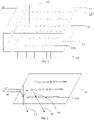
- a light guide plate 10 is provided.
- the light guide plate 10 is provided on a side thereof with an LED light bar 20, and the light guide plate 10 has a light emitting surface 11, a diffusion surface 12, and a light incident surface 13.
- the light incident surface 13 is located at a side of the light guide plate 10, and the light emitting surface 11 is arranged to be opposite to the light diffusion surface 12.
- the LED light bar 20 is arranged at an outer side of the light incident surface 13, light entering from the light incident surface 13 passes through second micro structures 120 on the light diffusion surface 12 and generates diffuse refraction and diffusion, so as to generate even and uniform light, which passes through first micro structures 110 on the light emitting surface 11 and enters a display panel.
- the first micro structures 110 protrude from the light emitting surface 11, and the first micro structures 110 are gradually tightly arranged on the light emitting surface 11 inwards from the light incident surface 13. Widths of the first micro structures 110 gradually reduce inwards from the light incident surface 13. Therefore, an arrangement density of the first micro structures gradually increases inwards from the light incident surface, and a penetration rate of light can be better increased.
- shapes of cross sections of the first micro structures comprise: semicircle, or semi ellipse, or other contours in any shapes protruding from the light emitting surface.
- light entering from the light incident surface passes through the second micro structures on the diffusion surface and generates diffuse reflection and diffusion, so as to generate even and uniform light. Accordingly, assuming that light 15 and light 18 are parallel light, the light 15 does not pass through the first micro structure 110, while the light 18 pass through the first micro structure 110; the light 15 generates reflection and refraction when passing through a plane in which a normal 17 is perpendicular to the light emitting surface 11, and reflected light 16 and refracted light 14 are generated. At this time, only the light 14 can pass through the light emitting surface 11.
- the light 15 when an incident angle of the light 15 is equal to or greater than a critical angle, the light 15 only generates reflection and does not generate refraction, that is, generates total reflection, and the light 15 is entirely unable to pass through the light emitting surface 11 (such a case is not shown in the drawings).
- the light 18 passes through the first micro structures 110, cross sections of the first micro structures 110 can be contours in any shape protruding from the light emitting surface 11; the light 15 does not pass through the first micro structures 110. Therefore, in comparison with the light 15, an incident angle of the light 18 reduces, and the light 18 is more uneasy to generate total reflection.
- a first micro structure 110 is regularly spherical, the light 18 passes through a spherical center of the first micro structure 110; the light 18 does not generate reflection and only generates refracted light 19, therefore a penetration rate of light can achieve the highest.
- a change amount of a distance between adjacent first micro structures is preferably 0.001-0.2mm.
- an average diameter of the first micro structures can be about 35 micrometers, and a height of a first micro structure can be 5 micrometers to 15 micrometers.
- the diffusion surface 12 is provided thereon with an array formed by the second micro structures 120 (the distribution of the second micro structures 120 in FIG. 1 is only schematic).
- the second micro structures 120 recess from the diffusion surface 12, and widths of the second micro structures 120 gradually increase inwards from the light incident surface 13.
- Light intensity near a light entering side of the light incident surface is stronger, and light intensity far away from the light entering side is weaker; therefore, it is possible to configure that volumes of second micro structures 120 near the light entering side is smaller, and configure that volumes of second micro structures 120 far away from the light entering side is larger, this is conducive for uniform distribution of light.
- a protruding height of the first micro structure is larger than a recessing depth of the second micro structure. It can be regarded that the recessing depth of the second micro structure is smaller. Furthermore, first, before light of an LED light source enters the light guide plate, a light incident angle can be preset using a reflection sheet, for example, an incident angle of light entering the diffusion surface is adjusted to an angle being larger than 44°; second, since the recessing depth of the second micro structure is smaller, an incident angle of light on the second micro structure can be approximately equal to an originally preset incident angle; finally, light not only can generate diffuse reflection and diffusion on the second micro structure, but also can generate total reflection, such that not only can the action of homogenizing light be achieved, but also light can generate total reflection on the diffusion surface. Thus, light can be avoided from passing through the diffusion surface, and a light utility rate is improved.
- the second micro structures are evenly arranged on the diffusion surface 12 inwards from the light incident surface, alternatively, the second micro structures are gradually tightly arranged on the diffusion surface 12 inwards from the light incident surface.
- a change amount of a distance between adjacent second micro structures is preferably 0.001-0.2mm.
- an average diameter of the second micro structures can be about 35 micrometers, and a height of a first micro structure can be 1 micrometer to 5 micrometers. Depths of the second micro structures are smaller, and a penetration rate for light to penetrate the light guide plate is lower.
- shapes of cross sections of the second micro structures can be fabricated into special shapes, such as circle, ellipse, arc, triangular, etc.
- processes of forming the first micro structures and/or the second micro structures can include at least: printing, hot pressing, etching, laser engraving, and injection molding processes.
- a light guide plate printing process may include the following steps: (1) providing an optical grade acrylic (PMMA)/polycarbonate (PS) or polystyrene (PS) light transmission plate, the light transmission plate has a light emitting surface for leading out light and a diffusion surface for diffusing light, the diffusion surface is arranged to be opposite to the light emitting surface; (2) printing a plurality of first micro structures using fast-drying IR curing ink on the light emitting surface of the light transmission plate, and printing a plurality of second micro structures on the diffusion surface; (3) placing the light transmission plate printed with the plurality of first microstructures and the plurality of second micro structures on a heating device controlled by a linear far-infrared programmable logic controller to perform heated curing in a stepped manner, thereby forming a light guide plate with the first micro structures and the second micro structures.
- PMMA optical grade acrylic
- PS polycarbonate
- PS polystyrene
- any point light source or line light source can be used as a light source, and then transformed into a planar light source.
- the light source can include an LED, a CCFL (cold cathode lamp), a fluorescent tube, and the like.
- the light guide plate 10 can be provided with an LED light source on one side of the light incident surface; alternatively, at least four LED light sources are embedded in four corners of the light guide plate, and the at least four LED light sources are arranged into a light source array. The arrangement should be as even as possible.
- the at least four LED light sources are connected in parallel and led to power wires to facilitate connection with a power supply.
- the at least four of the LED light sources are connected by copper wires to form a parallel relationship.
- the light guide plate has a light emitting surface configured to guide light out, the light emitting surface is provided with first micro structures, and the first micro structures protrude from the light emitting surface; the first micro structures are gradually tightly arranged on the light emitting surface inwards from the light incident surface; widths of the first micro structures gradually reduce inwards from the light incident surface.
- Light passes through the first micro structures protruding from the light emitting surface, an incident angle is reduced, so that the light is not prone to generate total reflection, a penetration rate of the light on the light emitting surface of the light guide plate is improved, and a light utility rate is increased.
- a reflective liquid crystal display screen is a liquid crystal display equipped with a reflector, so that ambient light is used as a light source of the liquid crystal display, and a front light module is also set as a supplementary light source, thus it has the advantages of energy saving, eye protection, etc.
- the display device can comprise a display panel 100, a light guide plate 200, optical glue 300, a color film substrate 400, and an array substrate 500, which are arranged layer by layer in sequence; wherein, point or line light sources, such as LED light sources, can be disposed at one side or four corners of the light guide plate 200.
- the light guide plate 200 has a light emitting surface, a diffusion surface, and a light incident surface, the light incident surface is located at a side surface of the light guide plate, and the light emitting surface is arranged to be opposite to the diffusion surface; an LED light bar is disposed on an outer side of the light incident surface, light entering from the light incident surface is reflected, refracted, and diffused by second micro structures on the diffusion surface to generate even and uniform light, which passes through first micro structures on the light emitting surface, and then passes through the optical glue 300, the color film substrate 400, and the array substrate 500 in sequence to supply light for the display panel 100 or other display components.
- the display panel 100 is preferably a touch panel.
- the LED light bar is disposed at a side of the light guide plate 200, the light guide plate 200 has the light emitting surface, the diffusion surface, and the light incident surface; the light incident surface is located at a side surface of the light guide plate 200, and the light emitting surface is arranged to be opposite to the diffusion surface; the LED light bar is disposed on an outer side of the light incident surface, light entering from the light incident surface passes through second micro structures on the diffusion surface and generates diffuse reflection and diffusion to generate even and uniform light, and then passes through the first micro structure on the light emitting surface and enters a display panel.
- the first micro structures protrude from the light emitting surface, and the first micro structures are gradually tightly arranged on the light emitting surface inwards from the light incident surface. Widths of the first micro structures gradually reduce inwards from the light incident surface. Therefore, an arrangement density of the first micro structures gradually increases inwards from the light incident surface, and a penetration rate of light can be better increased.
- shapes of cross sections of the first micro structures comprise: semicircle, or semi ellipse, or other contours in any shapes protruding from the light emitting surface.
- a change amount of a distance between adjacent first micro structures is preferably 0.001-0.2mm.
- an average diameter of the first micro structures can be about 35 micrometers, and a height of a first micro structure can be 5 micrometers to 15 micrometers.
- the diffusion surface is provided thereon with an array formed by the second micro structures.
- the second micro structures recess from the diffusion surface, and widths of the second micro structures gradually increase inwards from the light incident surface. Near a light entering side of the light incident surface, light intensity is stronger and volumes of the second micro structures are smaller; far away from the light entering side, light intensity is weaker and volumes of the second micro structures are larger; this is conducive for uniform distribution of light.
- a protruding height of the first micro structure is larger than a recessing depth of the second micro structure. It can be regarded that the recessing depth of the second micro structure is smaller. Furthermore, first, before light of an LED light source enters the light guide plate, a light incident angle can be preset using a reflection sheet, for example, an incident angle of light entering the diffusion surface is adjusted to an angle being larger than 44°; second, since the recessing depth of the second micro structure is smaller, an incident angle of light on the second micro structure can be approximately equal to an originally preset incident angle; finally, light not only can generate diffuse reflection and diffusion on the second micro structure, but also can generate total reflection, such that not only can the action of homogenizing light be achieved, but also light can generate total reflection on the diffusion surface. Thus, light can be avoided from passing through the diffusion surface, and a light utility rate is improved.
- the second micro structures are evenly arranged on the diffusion surface inwards from the light incident surface, alternatively, the second micro structures are gradually tightly arranged on the diffusion surface inwards from the light incident surface.
- a change amount of a distance between adjacent second micro structures is preferably 0.001-0.2mm.
- an average diameter of the second micro structures can be about 35 micrometers, and a height of a first micro structure can be 1 micrometer to 5 micrometers. Depths of the second micro structures are smaller, and a penetration rate for light to penetrate the light guide plate is lower.
- shapes of cross sections of the second micro structures can be fabricated into special shapes, such as circle, ellipse, arc, triangular, etc.
- processes of forming the first micro structures and/or the second micro structures can include at least: printing, hot pressing, etching, laser engraving, and injection molding processes.
- any point light source or line light source can be used as a light source, and then transformed into a planar light source.
- the light source can include an LED, a CCFL (cold cathode lamp), a fluorescent tube, and the like.
- the light guide plate can be provided with an LED light source on one side of the light incident surface; alternatively, at least four LED light sources are embedded in four corners of the light guide plate, and the at least four LED light sources are arranged into a light source array.
- the arrangement should be as even as possible.
- the at least four LED light sources are connected in parallel and led to power wires to facilitate connection with a power supply.
- the at least four of the LED light sources are connected by copper wires to form a parallel relationship.
- the display device can comprise a touch panel, a light guide plate, optical glue, a color film substrate, and an array substrate, which are arranged layer by layer in sequence.
- the light guide plate has a light emitting surface configured to guide light out, the light emitting surface is provided with first micro structures, and the first micro structures protrude from the light emitting surface; the first micro structures are gradually tightly arranged on the light emitting surface inwards from the light incident surface; widths of the first micro structures gradually reduce inwards from the light incident surface.
- Light passes through the first micro structures protruding from the light emitting surface, an incident angle is reduced, so that the light is not prone to generate total reflection, a penetration rate of the light on the light emitting surface of the light guide plate is improved, and a light utility rate is increased.
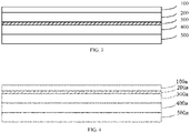
- the display device can comprise a display panel 100a, optical glue 200a, a color film substrate 300a, an array substrate 400a, and a light guide plate 500a, which are arranged layer by layer in sequence; wherein, point or line light sources, such as LED light sources, can be disposed at one side or four corners of the light guide plate 500a.
- the light guide plate 500a has a light emitting surface, a diffusion surface, and a light incident surface, the light incident surface is located at a side surface of the light guide plate, and the light emitting surface is arranged to be opposite to the diffusion surface; an LED light bar is disposed on an outer side of the light incident surface, light entering from the light incident surface is reflected, refracted, and diffused by second micro structures on the diffusion surface to generate even and uniform light, which passes through first micro structures on the light emitting surface, and then passes through the array substrate 400a, the color film substrate 300a, the optical glue 200a, and the display panel 100a in sequence to supply light for the display panel 100a or other display components.
- the display panel 100a is preferably a touch panel.
- the display device can comprise the display panel 100a, the optical glue 200a, the color film substrate 300a, the array substrate 400a, and the light guide plate 500a, which are arranged layer by layer in sequence.
- the light guide plate 500a has a light emitting surface configured to guide light out, the light emitting surface is provided with first micro structures, and the first micro structures protrude from the light emitting surface; the first micro structures are gradually tightly arranged on the light emitting surface inwards from the light incident surface; widths of the first micro structures gradually reduce inwards from the light incident surface.
- Light passes through the first micro structures protruding from the light emitting surface, an incident angle is reduced, so that the light is not prone to generate total reflection, a penetration rate of the light on the light emitting surface of the light guide plate is improved, and a light utility rate is increased.
- FIG. 5 shows a schematic structural diagram of the electronic device involved in embodiments of the present application.
- the electronic device may be a mobile phone, a computer, a digital broadcasting terminal, a message transceiving device, a game console, a tablet device, a medical equipment, a fitness equipment, a personal digital assistant, etc., specifically:
- the electronic device 1200 may include an RF (Radio Frequency) circuit 110, a memory 120 including one or more (only one is shown in the figure) computer-readable storage medium, an input unit 130, a display unit 140, a sensor 150, an audio circuit 160, a transmission module 170, a processor 180 including one or more (only one is shown in the figure) processing core, a power supply 190, and other components.
- RF Radio Frequency
- FIG. 5 does not constitute any limitation to the electronic device 1200, and may include more or less components than shown, or a combination of certain components, or a different arrangement of components.
- the RF circuit 110 is configured to receive and transmit electromagnetic waves, realize mutual conversion between electromagnetic waves and electric signals, and thereby communicate with a communication network or other devices.
- the RF circuit 110 may include various existing circuit elements for performing these functions, for example, an antenna, a radio frequency transceiver, a digital signal processor, an encryption/decryption chip, a subscriber identity module (SIM) card, a memory, and so on.
- the RF circuit 110 can communicate with various networks such as the Internet, an intranet, and a wireless network, or communicate with other devices through a wireless network.
- the memory 120 can be configured to store software programs and modules, such as the program instructions/modules corresponding to the screen state control method in the above embodiments.
- the processor 180 executes various functional applications and data processing by running the software programs and modules stored in the memory 120.
- the memory 120 may include a high-speed random access memory, and may also include a non-volatile memory, such as one or more magnetic storage devices, flash memory, or other non-volatile solid-state memories.
- the memory 120 may further include memories remotely provided relative to the processor 180, and these remote memories may be connected to the electronic device 1200 through a network. Examples of the aforementioned network include, but are not limited to, the Internet, corporate intranets, local area networks, mobile communication networks, and combinations thereof.
- the input unit 130 can be configured to receive input digital or character information, and generate keyboard, mouse, joystick, optical or trackball signal input related to user settings and function control.
- the input unit 130 may include a touch sensitive surface 131 and other input devices 132.
- the touch sensitive surface 131 also called a touch screen or a touch pad, can collect users' touch operations on or near it (for example, users use any suitable objects or accessories, such as fingers, stylus, etc., to operate on the touch sensitive surface 131 or near the touch sensitive surface 131), and drive corresponding connection devices according to a preset program.
- the input unit 130 may also include other input devices 132.
- the other input device 132 may include, but is not limited to, one or more of a physical keyboard, function keys (such as a volume control button, a switch button, etc.), a trackball, a mouse, a joystick, and so on.
- function keys such as a volume control button, a switch button, etc.
- a trackball such as a mouse, a joystick, and so on.
- the display device 140 can be configured to display information input by users, information provided to users, and various graphical user interfaces of the electronic device 1200. These graphical user interfaces may be composed of graphics, texts, icons, videos, and any combination thereof.
- the display device 140 may include a display panel 141.
- the display device 140 can comprise a touch panel, a light guide plate, optical glue, a color film substrate, and an array substrate which are arranged layer by layer in sequence, or a touch panel, optical glue, a color film substrate, an array substrate, and a light guide plate which are arranged layer by layer in sequence.
- point or line light sources such as LED light sources
- the light guide plate 200 has a light emitting surface, a diffusion surface, and a light incident surface, the light incident surface is located at a side surface of the light guide plate, and the light emitting surface is arranged to be opposite to the diffusion surface; an LED light bar is disposed on an outer side of the light incident surface, light entering from the light incident surface is reflected, refracted, and diffused by second micro structures on the diffusion surface to generate even and uniform light.
- the LED light bar is disposed at a side of the light guide plate, the light guide plate has a light emitting surface, a diffusion surface, and a light incident surface, the light incident surface is located at a side surface of the light guide plate, and the light emitting surface is arranged to be opposite to the diffusion surface.
- the LED light bar is disposed on an outer side of the light incident surface, light entering from the light incident surface passes through second micro structures on the light diffusion surface and generates diffuse refraction and diffusion, so as to generate even and uniform light, which passes through first micro structures on the light emitting surface and enters a display panel.
- the first micro structures protrude from the light emitting surface, and the first micro structures are gradually tightly arranged on the light emitting surface inwards from the light incident surface. Widths of the first micro structures gradually reduce inwards from the light incident surface. Therefore, an arrangement density of the first micro structures gradually increases inwards from the light incident surface, and a penetration rate of light can be better increased.
- shapes of cross sections of the first micro structures comprise: semicircle, or semi ellipse, or other contours in any shapes protruding from the light emitting surface.
- a change amount of a distance between adjacent first micro structures is preferably 0.001-0.2mm.
- an average diameter of the first micro structures can be about 35 micrometers, and a height of a first micro structure can be 5 micrometers to 15 micrometers.
- the diffusion surface is provided thereon with an array formed by the second micro structures.
- the second micro structures recess from the diffusion surface, and widths of the second micro structures gradually increase inwards from the light incident surface. Near a light entering side of the light incident surface, light intensity is stronger and volumes of the second micro structures are smaller; far away from the light entering side, light intensity is weaker and volumes of the second micro structures are larger; this is conducive for uniform distribution of light.
- a protruding height of the first micro structure is larger than a recessing depth of the second micro structure. It can be regarded that the recessing depth of the second micro structure is smaller. Furthermore, first, before light of an LED light source enters the light guide plate, a light incident angle can be preset using a reflection sheet, for example, an incident angle of light entering the diffusion surface is adjusted to an angle being larger than 44°; second, since the recessing depth of the second micro structure is smaller, an incident angle of light on the second micro structure can be approximately equal to an originally preset incident angle; finally, light not only can generate diffuse reflection and diffusion on the second micro structure, but also can generate total reflection, such that not only can the action of homogenizing light be achieved, but also light can generate total reflection on the diffusion surface. Thus, light can be avoided from passing through the diffusion surface, and a light utility rate is improved.
- the second micro structures are evenly arranged on the diffusion surface inwards from the light incident surface, alternatively, the second micro structures are gradually tightly arranged on the diffusion surface inwards from the light incident surface.
- a change amount of a distance between adjacent second micro structures is preferably 0.001-0.2mm.
- an average diameter of the second micro structures can be about 35 micrometers, and a height of a first micro structure can be 1 micrometer to 5 micrometers. Depths of the second micro structures are smaller, and a penetration rate for light to penetrate the light guide plate is lower.
- shapes of cross sections of the second micro structures can be fabricated into special shapes, such as circle, ellipse, arc, triangular, etc.
- processes of forming the first micro structures and/or the second micro structures can include at least: printing, hot pressing, etching, laser engraving, and injection molding processes.
- any point light source or line light source can be used as a light source, and then transformed into a planar light source.
- the light source can include an LED, a CCFL (cold cathode lamp), a fluorescent tube, and the like.
- the light guide plate can be provided with an LED light source on one side of the light incident surface; alternatively, at least four LED light sources are embedded in four corners of the light guide plate, and the at least four LED light sources are arranged into a light source array.
- the arrangement should be as even as possible.
- the at least four LED light sources are connected in parallel and led to power wires to facilitate connection with a power supply.
- the at least four of the LED light sources are connected by copper wires to form a parallel relationship.
- an electronic device comprises a display device
- the display device can comprise: a touch panel, a light guide plate, optical glue, a color film substrate, and an array substrate which are arranged layer by layer in sequence, or a touch panel, optical glue, a color film substrate, an array substrate, and a light guide plate which are arranged layer by layer in sequence.
- the light guide plate has a light emitting surface configured to guide light out, the light emitting surface is provided with first micro structures, and the first micro structures protrude from the light emitting surface; the first micro structures are gradually tightly arranged on the light emitting surface inwards from the light incident surface; widths of the first micro structures gradually reduce inwards from the light incident surface.
- Light passes through the first micro structures protruding from the light emitting surface, an incident angle is reduced, so that the light is not prone to generate total reflection, a penetration rate of the light on the light emitting surface of the light guide plate is improved, and a light utility rate is increased.
- the electronic device 1200 may further include at least one kind of sensor 150, such as a light sensor, a motion sensor, and other sensors.
- sensor 150 such as a light sensor, a motion sensor, and other sensors.
- other sensors such as a barometer, a hygrometer, a thermometer, an infrared sensor, etc., which can be further configured for the electronic device 1200, they will not be repeated here.
- the audio circuit 160, the speaker 161, and the microphone 162 can provide an audio interface between a user and the electronic device 1200.
- the audio circuit 160 can transmit an electrical signal converted from the received audio data to the speaker 161, and it is converted into a sound signal for output by the speaker 161; on the other hand, the microphone 162 converts a collected sound signal into an electrical signal, which is received by the audio circuit 160 and converted into audio data; the audio data is then output to the processor 180 to process, and sent to, for example, another terminal via the RF circuit 110, or the audio data is output to the memory 120 for further processing.
- the audio circuit 160 may also include an earplug jack to provide communication between a peripheral earphone and the electronic device 1200.
- the electronic device 1200 can help users send and receive emails, browse web pages, and access streaming media through the transmission module 170 (e.g., a Wi-Fi module), and it provides users with wireless broadband Internet access.
- the transmission module 170 e.g., a Wi-Fi module
- FIG. 5 shows the transmission module 170, it is understandable that it is not a necessary component of the electronic device 1200, and can be omitted as needed without changing the essence of the invention.
- the processor 180 is the control center of the electronic device 1200. It uses various interfaces and lines to connect various parts of an entire mobile phone, performs various functions of the electronic device 1200 and processes data by running or executing software programs and/or modules stored in the memory 120 and calling data stored in the memory 120, and thereby monitors the mobile phone as a whole.
- the processor 180 may include one or more processing cores; in some embodiments, the processor 180 may integrate an application processor and a modem processor, wherein the application processor mainly processes an operating system, a user interface, application programs, etc., and the modem processor mainly processes wireless communication. It can be understood that the foregoing modem processor may also not be integrated into the processor 180.
- the electronic device 1200 further includes a power source 190 (such as a battery) for supplying power to various components.
- the power source may be logically connected to the processor 180 through a power management system, and thereby realize functions such as charging management, discharging, and power management through the power management system.
- the power supply 190 may also include any components such as one or more DC or AC power supply, a recharging system, a power failure detection circuit, a power converter or inverter, a power status indicator, and so on.
- the electronic device 1200 may also include a camera (such as a front camera, a rear camera), a Bluetooth module, etc., which will not be repeated here.
- the display unit 140 of the electronic device 1200 is a touch screen display, and the electronic device 1200 further includes a memory 120 and one or more program, wherein the one or more program is stored in the memory 120 and configured in such a way that the program stored in the memory 120 is executed by one or more processor 180 to realize various functions.
- a light guide plate provided by embodiments of the present application is described in detail above, and specific examples are used in this disclosure to describe principles and implementations of the present application.
- the description of the above embodiments is only used to help understand technical solutions of the present application and their core ideas.
- Those of ordinary skill in the art should understand that: they can still modify the technical solutions recorded in the foregoing embodiments, or equivalently replace some technical features therein; these modifications or replacements do not make the essence of corresponding technical solutions deviate from the scope of the technical solutions of the embodiments of the present application.
Landscapes
- Physics & Mathematics (AREA)
- General Physics & Mathematics (AREA)
- Optics & Photonics (AREA)
- Nonlinear Science (AREA)
- Mathematical Physics (AREA)
- Chemical & Material Sciences (AREA)
- Crystallography & Structural Chemistry (AREA)
- Engineering & Computer Science (AREA)
- Microelectronics & Electronic Packaging (AREA)
- Planar Illumination Modules (AREA)
Abstract
Description
- The present application relates to the field of display technology, and in particular, to a light guide plate and a display device.
- At present, in a liquid crystal display device, liquid crystal molecules themselves cannot emit light, therefore an independent light source is required. An optical module usually comprises at least an LED lamp and a light guide plate, the light guide plate is provided thereon with micro structures, such as dots; the LED lamp is transformed into a planar light source through the dots to provide a light source for a display panel. However, much light is prone to generate reflection on a light emitting surface of the light guide plate and return into the light guide plate, therefore it cannot pass through the light emitting surface of the light guide plate, and a problem of a low light utility rate exists.
- Embodiments of the present application provides a light guide plate and a display device, which can reduce emission of light on a light emitting surface of the light guide plate, increase a penetration rate of light, and thereby increase a light utility rate.
- A first aspect of the present application provides a light guide plate, the light guide plate has a light emitting surface configured to guide light out, the light emitting surface is provided with first micro structures, and the first micro structures protrude from the light emitting surface.
- A second aspect of the present application provides a display device comprising a display panel and a light guide plate configured to supply light to the display panel, wherein the light guide plate comprises a light emitting surface configured to guide light out, the light emitting surface is provided with first micro structures, and the first micro structures protrude from the light emitting surface.
- Embodiments of the present application provides a light guide plate and a display device. The light guide plate has a light emitting surface configured to guide light out, the light emitting surface is provided with first micro structures, and the first micro structures protrude from the light emitting surface; the light guide plate further has a diffusion surface configured for light diffusion, the diffusion surface is arranged to be opposite to the light emitting surface, the diffusion surface is provided with second micro structures, and the second micro structures recess from the diffusion surface; a protruding height of the first micro structure is larger than a recessing depth of the second micro structure; the first micro structures are gradually tightly arranged on the light emitting surface inwards from the light incident surface; widths of the first micro structures gradually reduce inwards from the light incident surface; and widths of the second micro structures gradually increase inwards from the light incident surface. Therefore, light beams form even and uniform light through diffuse reflection and diffusion on the second micro structures, the light passes through the protruding structure of the first micro structures, an incident angle is reduced, total reflection is not prone to occur, and refraction is easier to occur, so that the light passes through the light emitting surface; a penetration rate of light on the light emitting surface of the light guide plate is improved, and a light utility rate is increased.
- Technical solutions and other advantageous effect of the present application will become apparent by describing specific embodiments of the present application in detail in accompany with the drawings below.
-
FIG. 1 is a schematic view of a light guide plate provided by an embodiment of the present application. -
FIG. 2 is a schematic view of a light emitting surface provided by an embodiment of the present application. -
FIG. 3 is a schematic view of a reflection-type liquid crystal display provided by an embodiment of the present application. -
FIG. 4 is a schematic view of another liquid crystal display provided by an embodiment of the present application. -
FIG. 5 is a structural schematic view of an electronic device provided by an embodiment of the present application. - Technical solutions in embodiments of the present application will be described clearly and completely below in accompany with drawings in embodiments of the present application. Obviously, the described embodiments are merely some embodiments of the present application, but not all embodiments. Based on embodiments of the present application, all other embodiments obtained by one of ordinary skill in the art without paying any creative work belong to the protection scope of the present application.
- In the description of the present application, it needs to be understood that orientations or positional relationships indicated by the terms "length", "width", "height", "depth", and so on are based on orientations or positional relationships shown in the drawings, which are only intended to facilitate the description of the present application and simplify the description, but not to indicate or imply that devices or elements referred to must have specific orientations or be configured and operated in specific orientations, and therefore cannot be understood as any limitation to the present application. In addition, terms "first" and "second" are only used for descriptive purposes, and cannot be understood as indicating or implying relative importance or implicitly indicating the number of indicated technical features. Therefore, features defined with "first" and "second" may explicitly or implicitly include one or more such feature(s). In the description of the present application, "multiple" means two or more than two, unless otherwise specifically defined.
- The following disclosure provides many different embodiments or examples for realizing different structures of the present application. In order to simplify the disclosure of the present application, components and settings of specific examples are described below. Of course, they are only examples, and are not intended to limit the present application. In addition, the present application may repeat reference numerals and/or reference letters in different examples, and this repetition is for the purpose of simplification and clarity, itself does not indicate any relationship between various embodiments and/or settings as discussed. In addition, the present application provides examples of various specific processes and materials, but those of ordinary skill in the art may be aware of application of other processes and/or use of other materials.
- A first aspect of the present application provides a light guide plate comprising a light emitting surface configured to guide light out, wherein the light emitting surface is provided with first micro structures, and the first micro structures protrude from the light emitting surface.
- In some embodiments, the light guide plate further comprises a diffusion surface configured for light diffusion, wherein the diffusion surface is arranged to be opposite to the light emitting surface, the diffusion surface is provided with second micro structures, and the second micro structures recess from the diffusion surface.
- In some embodiments, a protruding height of the first micro structure is larger than a recessing depth of the second micro structure.
- In some embodiments, the light guide plate further comprises a light incident surface, wherein the light incident surface is an end surface of the light guide plate, and the light incident surface is adjacent to the light emitting surface and the diffusion surface respectively; the first micro structures are gradually tightly arranged on the light emitting surface inwards from the light incident surface.
- In some embodiments, widths of the first micro structures gradually reduce inwards from the light incident surface.
- In some embodiments, widths of the second micro structures gradually increase inwards from the light incident surface.
- In some embodiments, processes of forming the first micro structures include at least: printing, hot pressing, etching, engraving, and injection molding processes.
- In some embodiments, shapes of cross sections of the second micro structures comprise: circle, ellipse, arc, and triangular.
- In some embodiments, shapes of cross sections of the first micro structures comprise: semicircle or semi ellipse.
- A second aspect of the present application provides a display device comprising a display panel and a light guide plate configured to supply light to the display panel, wherein the light guide plate comprises a light emitting surface configured to guide light out, the light emitting surface is provided with first micro structures, and the first micro structures protrude from the light emitting surface.
- In some embodiments, the display device further comprises: optical glue, a color film substrate, and an array substrate; wherein the display panel, the light guide plate, the optical glue, the color film substrate, and the array substrate are arranged layer by layer in sequence.
- In some embodiments, the display device further comprises: optical glue, a color film substrate, and an array substrate; wherein the display panel, the optical glue, the color film substrate, the array substrate, and the light guide plate are arranged layer by layer in sequence.
- In some embodiments, wherein the light guide plate further comprises a diffusion surface configured for light diffusion, the diffusion surface is arranged to be opposite to the light emitting surface, the diffusion surface is provided with second micro structures, and the second micro structures recess from the diffusion surface.
- In some embodiments, a protruding height of the first micro structure is larger than a recessing depth of the second micro structure.
- In some embodiments, the light guide plate further comprises a light incident surface, the light incident surface is an end surface of the light guide plate, and the light incident surface is adjacent to the light emitting surface and the diffusion surface respectively; the first micro structures are gradually tightly arranged on the light emitting surface inwards from the light incident surface.
- Referring to
FIG. 1 , alight guide plate 10 is provided. Thelight guide plate 10 is provided on a side thereof with anLED light bar 20, and thelight guide plate 10 has alight emitting surface 11, adiffusion surface 12, and alight incident surface 13. Thelight incident surface 13 is located at a side of thelight guide plate 10, and thelight emitting surface 11 is arranged to be opposite to thelight diffusion surface 12. TheLED light bar 20 is arranged at an outer side of thelight incident surface 13, light entering from thelight incident surface 13 passes through secondmicro structures 120 on thelight diffusion surface 12 and generates diffuse refraction and diffusion, so as to generate even and uniform light, which passes through firstmicro structures 110 on thelight emitting surface 11 and enters a display panel. - Specifically, the first
micro structures 110 protrude from thelight emitting surface 11, and the firstmicro structures 110 are gradually tightly arranged on thelight emitting surface 11 inwards from thelight incident surface 13. Widths of the firstmicro structures 110 gradually reduce inwards from thelight incident surface 13. Therefore, an arrangement density of the first micro structures gradually increases inwards from the light incident surface, and a penetration rate of light can be better increased. - In some embodiments, shapes of cross sections of the first micro structures comprise: semicircle, or semi ellipse, or other contours in any shapes protruding from the light emitting surface.
- When light is emitted from an optically dense medium to an interface with an optically thinner medium, and an incident angle is equal to or greater than a critical angle, the light will be totally reflected. At present, a commonly used material of light guide plates is an optical grade acrylic material, its refractive index is about 1.4. It can be concluded that total reflection will occur when an incident angle of incident light is equal to or greater than 44°.
- Referring to
FIG. 2 , light entering from the light incident surface passes through the second micro structures on the diffusion surface and generates diffuse reflection and diffusion, so as to generate even and uniform light. Accordingly, assuming thatlight 15 andlight 18 are parallel light, thelight 15 does not pass through the firstmicro structure 110, while thelight 18 pass through the firstmicro structure 110; thelight 15 generates reflection and refraction when passing through a plane in which a normal 17 is perpendicular to thelight emitting surface 11, and reflectedlight 16 and refractedlight 14 are generated. At this time, only thelight 14 can pass through thelight emitting surface 11. Wherein, when an incident angle of thelight 15 is equal to or greater than a critical angle, thelight 15 only generates reflection and does not generate refraction, that is, generates total reflection, and thelight 15 is entirely unable to pass through the light emitting surface 11 (such a case is not shown in the drawings). - Continuing to refer to
FIG. 2 , thelight 18 passes through the firstmicro structures 110, cross sections of the firstmicro structures 110 can be contours in any shape protruding from thelight emitting surface 11; thelight 15 does not pass through the firstmicro structures 110. Therefore, in comparison with thelight 15, an incident angle of thelight 18 reduces, and thelight 18 is more uneasy to generate total reflection. When a firstmicro structure 110 is regularly spherical, the light 18 passes through a spherical center of the firstmicro structure 110; the light 18 does not generate reflection and only generates refracted light 19, therefore a penetration rate of light can achieve the highest. - In some embodiments, a change amount of a distance between adjacent first micro structures is preferably 0.001-0.2mm.
- In some embodiments, an average diameter of the first micro structures can be about 35 micrometers, and a height of a first micro structure can be 5 micrometers to 15 micrometers.
- Specifically, the
diffusion surface 12 is provided thereon with an array formed by the second micro structures 120 (the distribution of the secondmicro structures 120 inFIG. 1 is only schematic). The secondmicro structures 120 recess from thediffusion surface 12, and widths of the secondmicro structures 120 gradually increase inwards from thelight incident surface 13. Light intensity near a light entering side of the light incident surface is stronger, and light intensity far away from the light entering side is weaker; therefore, it is possible to configure that volumes of secondmicro structures 120 near the light entering side is smaller, and configure that volumes of secondmicro structures 120 far away from the light entering side is larger, this is conducive for uniform distribution of light. - In some embodiments, a protruding height of the first micro structure is larger than a recessing depth of the second micro structure. It can be regarded that the recessing depth of the second micro structure is smaller. Furthermore, first, before light of an LED light source enters the light guide plate, a light incident angle can be preset using a reflection sheet, for example, an incident angle of light entering the diffusion surface is adjusted to an angle being larger than 44°; second, since the recessing depth of the second micro structure is smaller, an incident angle of light on the second micro structure can be approximately equal to an originally preset incident angle; finally, light not only can generate diffuse reflection and diffusion on the second micro structure, but also can generate total reflection, such that not only can the action of homogenizing light be achieved, but also light can generate total reflection on the diffusion surface. Thus, light can be avoided from passing through the diffusion surface, and a light utility rate is improved.
- In some embodiments, the second micro structures are evenly arranged on the
diffusion surface 12 inwards from the light incident surface, alternatively, the second micro structures are gradually tightly arranged on thediffusion surface 12 inwards from the light incident surface. - In some embodiments, a change amount of a distance between adjacent second micro structures is preferably 0.001-0.2mm.
- In some embodiments, an average diameter of the second micro structures can be about 35 micrometers, and a height of a first micro structure can be 1 micrometer to 5 micrometers. Depths of the second micro structures are smaller, and a penetration rate for light to penetrate the light guide plate is lower.
- In some embodiments, shapes of cross sections of the second micro structures can be fabricated into special shapes, such as circle, ellipse, arc, triangular, etc.
- In some embodiments, processes of forming the first micro structures and/or the second micro structures can include at least: printing, hot pressing, etching, laser engraving, and injection molding processes.
- Specifically, a light guide plate printing process may include the following steps: (1) providing an optical grade acrylic (PMMA)/polycarbonate (PS) or polystyrene (PS) light transmission plate, the light transmission plate has a light emitting surface for leading out light and a diffusion surface for diffusing light, the diffusion surface is arranged to be opposite to the light emitting surface; (2) printing a plurality of first micro structures using fast-drying IR curing ink on the light emitting surface of the light transmission plate, and printing a plurality of second micro structures on the diffusion surface; (3) placing the light transmission plate printed with the plurality of first microstructures and the plurality of second micro structures on a heating device controlled by a linear far-infrared programmable logic controller to perform heated curing in a stepped manner, thereby forming a light guide plate with the first micro structures and the second micro structures.
- In some embodiments, any point light source or line light source can be used as a light source, and then transformed into a planar light source. The light source can include an LED, a CCFL (cold cathode lamp), a fluorescent tube, and the like.
- In some embodiments, the
light guide plate 10 can be provided with an LED light source on one side of the light incident surface; alternatively, at least four LED light sources are embedded in four corners of the light guide plate, and the at least four LED light sources are arranged into a light source array. The arrangement should be as even as possible. The at least four LED light sources are connected in parallel and led to power wires to facilitate connection with a power supply. The at least four of the LED light sources are connected by copper wires to form a parallel relationship. - From the above, it can be known that embodiments of the present application provide a light guide plate. The light guide plate has a light emitting surface configured to guide light out, the light emitting surface is provided with first micro structures, and the first micro structures protrude from the light emitting surface; the first micro structures are gradually tightly arranged on the light emitting surface inwards from the light incident surface; widths of the first micro structures gradually reduce inwards from the light incident surface. Light passes through the first micro structures protruding from the light emitting surface, an incident angle is reduced, so that the light is not prone to generate total reflection, a penetration rate of the light on the light emitting surface of the light guide plate is improved, and a light utility rate is increased.
- Another embodiment of the present application provides a display device, and specifically relates to a reflective liquid crystal display device. A reflective liquid crystal display screen is a liquid crystal display equipped with a reflector, so that ambient light is used as a light source of the liquid crystal display, and a front light module is also set as a supplementary light source, thus it has the advantages of energy saving, eye protection, etc.
- Referring to
FIG. 3 , the display device can comprise adisplay panel 100, alight guide plate 200,optical glue 300, acolor film substrate 400, and anarray substrate 500, which are arranged layer by layer in sequence; wherein, point or line light sources, such as LED light sources, can be disposed at one side or four corners of thelight guide plate 200. Thelight guide plate 200 has a light emitting surface, a diffusion surface, and a light incident surface, the light incident surface is located at a side surface of the light guide plate, and the light emitting surface is arranged to be opposite to the diffusion surface; an LED light bar is disposed on an outer side of the light incident surface, light entering from the light incident surface is reflected, refracted, and diffused by second micro structures on the diffusion surface to generate even and uniform light, which passes through first micro structures on the light emitting surface, and then passes through theoptical glue 300, thecolor film substrate 400, and thearray substrate 500 in sequence to supply light for thedisplay panel 100 or other display components. Thedisplay panel 100 is preferably a touch panel. - In the
light guide plate 200, the LED light bar is disposed at a side of thelight guide plate 200, thelight guide plate 200 has the light emitting surface, the diffusion surface, and the light incident surface; the light incident surface is located at a side surface of thelight guide plate 200, and the light emitting surface is arranged to be opposite to the diffusion surface; the LED light bar is disposed on an outer side of the light incident surface, light entering from the light incident surface passes through second micro structures on the diffusion surface and generates diffuse reflection and diffusion to generate even and uniform light, and then passes through the first micro structure on the light emitting surface and enters a display panel. - Specifically, the first micro structures protrude from the light emitting surface, and the first micro structures are gradually tightly arranged on the light emitting surface inwards from the light incident surface. Widths of the first micro structures gradually reduce inwards from the light incident surface. Therefore, an arrangement density of the first micro structures gradually increases inwards from the light incident surface, and a penetration rate of light can be better increased.
- In some embodiments, shapes of cross sections of the first micro structures comprise: semicircle, or semi ellipse, or other contours in any shapes protruding from the light emitting surface.
- In some embodiments, a change amount of a distance between adjacent first micro structures is preferably 0.001-0.2mm.
- In some embodiments, an average diameter of the first micro structures can be about 35 micrometers, and a height of a first micro structure can be 5 micrometers to 15 micrometers.
- Specifically, the diffusion surface is provided thereon with an array formed by the second micro structures. The second micro structures recess from the diffusion surface, and widths of the second micro structures gradually increase inwards from the light incident surface. Near a light entering side of the light incident surface, light intensity is stronger and volumes of the second micro structures are smaller; far away from the light entering side, light intensity is weaker and volumes of the second micro structures are larger; this is conducive for uniform distribution of light.
- In some embodiments, a protruding height of the first micro structure is larger than a recessing depth of the second micro structure. It can be regarded that the recessing depth of the second micro structure is smaller. Furthermore, first, before light of an LED light source enters the light guide plate, a light incident angle can be preset using a reflection sheet, for example, an incident angle of light entering the diffusion surface is adjusted to an angle being larger than 44°; second, since the recessing depth of the second micro structure is smaller, an incident angle of light on the second micro structure can be approximately equal to an originally preset incident angle; finally, light not only can generate diffuse reflection and diffusion on the second micro structure, but also can generate total reflection, such that not only can the action of homogenizing light be achieved, but also light can generate total reflection on the diffusion surface. Thus, light can be avoided from passing through the diffusion surface, and a light utility rate is improved.
- In some embodiments, the second micro structures are evenly arranged on the diffusion surface inwards from the light incident surface, alternatively, the second micro structures are gradually tightly arranged on the diffusion surface inwards from the light incident surface.
- In some embodiments, a change amount of a distance between adjacent second micro structures is preferably 0.001-0.2mm.
- In some embodiments, an average diameter of the second micro structures can be about 35 micrometers, and a height of a first micro structure can be 1 micrometer to 5 micrometers. Depths of the second micro structures are smaller, and a penetration rate for light to penetrate the light guide plate is lower.
- In some embodiments, shapes of cross sections of the second micro structures can be fabricated into special shapes, such as circle, ellipse, arc, triangular, etc.
- In some embodiments, processes of forming the first micro structures and/or the second micro structures can include at least: printing, hot pressing, etching, laser engraving, and injection molding processes.
- In some embodiments, any point light source or line light source can be used as a light source, and then transformed into a planar light source. The light source can include an LED, a CCFL (cold cathode lamp), a fluorescent tube, and the like.
- In some embodiments, the light guide plate can be provided with an LED light source on one side of the light incident surface; alternatively, at least four LED light sources are embedded in four corners of the light guide plate, and the at least four LED light sources are arranged into a light source array. The arrangement should be as even as possible. The at least four LED light sources are connected in parallel and led to power wires to facilitate connection with a power supply. The at least four of the LED light sources are connected by copper wires to form a parallel relationship.
- From the above, it can be known that embodiments of the present application provide a display device, the display device can comprise a touch panel, a light guide plate, optical glue, a color film substrate, and an array substrate, which are arranged layer by layer in sequence. The light guide plate has a light emitting surface configured to guide light out, the light emitting surface is provided with first micro structures, and the first micro structures protrude from the light emitting surface; the first micro structures are gradually tightly arranged on the light emitting surface inwards from the light incident surface; widths of the first micro structures gradually reduce inwards from the light incident surface. Light passes through the first micro structures protruding from the light emitting surface, an incident angle is reduced, so that the light is not prone to generate total reflection, a penetration rate of the light on the light emitting surface of the light guide plate is improved, and a light utility rate is increased.
- Another embodiment of the present application provides a display device, which specifically relates to a liquid crystal display device. This display device, in comparison with the display device provided by the above embodiments, mainly differs in that: referring to
FIG. 4 , the display device can comprise adisplay panel 100a,optical glue 200a, acolor film substrate 300a, anarray substrate 400a, and alight guide plate 500a, which are arranged layer by layer in sequence; wherein, point or line light sources, such as LED light sources, can be disposed at one side or four corners of thelight guide plate 500a. Thelight guide plate 500a has a light emitting surface, a diffusion surface, and a light incident surface, the light incident surface is located at a side surface of the light guide plate, and the light emitting surface is arranged to be opposite to the diffusion surface; an LED light bar is disposed on an outer side of the light incident surface, light entering from the light incident surface is reflected, refracted, and diffused by second micro structures on the diffusion surface to generate even and uniform light, which passes through first micro structures on the light emitting surface, and then passes through thearray substrate 400a, thecolor film substrate 300a, theoptical glue 200a, and thedisplay panel 100a in sequence to supply light for thedisplay panel 100a or other display components. Thedisplay panel 100a is preferably a touch panel. - From the above, it can be known that embodiments of the present application provide a display device, the display device can comprise the
display panel 100a, theoptical glue 200a, thecolor film substrate 300a, thearray substrate 400a, and thelight guide plate 500a, which are arranged layer by layer in sequence. Thelight guide plate 500a has a light emitting surface configured to guide light out, the light emitting surface is provided with first micro structures, and the first micro structures protrude from the light emitting surface; the first micro structures are gradually tightly arranged on the light emitting surface inwards from the light incident surface; widths of the first micro structures gradually reduce inwards from the light incident surface. Light passes through the first micro structures protruding from the light emitting surface, an incident angle is reduced, so that the light is not prone to generate total reflection, a penetration rate of the light on the light emitting surface of the light guide plate is improved, and a light utility rate is increased. - A display device in embodiments of the present application is described above, and the electronic equipment in embodiments of the present application is described below from the perspective of hardware processing. Embodiments of the present application further provide an electronic device, as shown in
FIG. 5 , which shows a schematic structural diagram of the electronic device involved in embodiments of the present application. The electronic device may be a mobile phone, a computer, a digital broadcasting terminal, a message transceiving device, a game console, a tablet device, a medical equipment, a fitness equipment, a personal digital assistant, etc., specifically: - The
electronic device 1200 may include an RF (Radio Frequency)circuit 110, amemory 120 including one or more (only one is shown in the figure) computer-readable storage medium, aninput unit 130, adisplay unit 140, asensor 150, anaudio circuit 160, atransmission module 170, aprocessor 180 including one or more (only one is shown in the figure) processing core, apower supply 190, and other components. Those skilled in the art can understand that the structure of theelectronic device 1200 shown inFIG. 5 does not constitute any limitation to theelectronic device 1200, and may include more or less components than shown, or a combination of certain components, or a different arrangement of components. Wherein: - The
RF circuit 110 is configured to receive and transmit electromagnetic waves, realize mutual conversion between electromagnetic waves and electric signals, and thereby communicate with a communication network or other devices. TheRF circuit 110 may include various existing circuit elements for performing these functions, for example, an antenna, a radio frequency transceiver, a digital signal processor, an encryption/decryption chip, a subscriber identity module (SIM) card, a memory, and so on. TheRF circuit 110 can communicate with various networks such as the Internet, an intranet, and a wireless network, or communicate with other devices through a wireless network. - The
memory 120 can be configured to store software programs and modules, such as the program instructions/modules corresponding to the screen state control method in the above embodiments. Theprocessor 180 executes various functional applications and data processing by running the software programs and modules stored in thememory 120. Thememory 120 may include a high-speed random access memory, and may also include a non-volatile memory, such as one or more magnetic storage devices, flash memory, or other non-volatile solid-state memories. In some embodiments, thememory 120 may further include memories remotely provided relative to theprocessor 180, and these remote memories may be connected to theelectronic device 1200 through a network. Examples of the aforementioned network include, but are not limited to, the Internet, corporate intranets, local area networks, mobile communication networks, and combinations thereof. - The
input unit 130 can be configured to receive input digital or character information, and generate keyboard, mouse, joystick, optical or trackball signal input related to user settings and function control. Specifically, theinput unit 130 may include a touchsensitive surface 131 andother input devices 132. The touchsensitive surface 131, also called a touch screen or a touch pad, can collect users' touch operations on or near it (for example, users use any suitable objects or accessories, such as fingers, stylus, etc., to operate on the touchsensitive surface 131 or near the touch sensitive surface 131), and drive corresponding connection devices according to a preset program. In addition to the touchsensitive surface 131, theinput unit 130 may also includeother input devices 132. Specifically, theother input device 132 may include, but is not limited to, one or more of a physical keyboard, function keys (such as a volume control button, a switch button, etc.), a trackball, a mouse, a joystick, and so on. - The
display device 140 can be configured to display information input by users, information provided to users, and various graphical user interfaces of theelectronic device 1200. These graphical user interfaces may be composed of graphics, texts, icons, videos, and any combination thereof. Thedisplay device 140 may include adisplay panel 141. - The
display device 140 can comprise a touch panel, a light guide plate, optical glue, a color film substrate, and an array substrate which are arranged layer by layer in sequence, or a touch panel, optical glue, a color film substrate, an array substrate, and a light guide plate which are arranged layer by layer in sequence. - Wherein, point or line light sources, such as LED light sources, can be disposed at one side or four corners of the light guide plate. The
light guide plate 200 has a light emitting surface, a diffusion surface, and a light incident surface, the light incident surface is located at a side surface of the light guide plate, and the light emitting surface is arranged to be opposite to the diffusion surface; an LED light bar is disposed on an outer side of the light incident surface, light entering from the light incident surface is reflected, refracted, and diffused by second micro structures on the diffusion surface to generate even and uniform light. - The LED light bar is disposed at a side of the light guide plate, the light guide plate has a light emitting surface, a diffusion surface, and a light incident surface, the light incident surface is located at a side surface of the light guide plate, and the light emitting surface is arranged to be opposite to the diffusion surface. The LED light bar is disposed on an outer side of the light incident surface, light entering from the light incident surface passes through second micro structures on the light diffusion surface and generates diffuse refraction and diffusion, so as to generate even and uniform light, which passes through first micro structures on the light emitting surface and enters a display panel.
- Specifically, the first micro structures protrude from the light emitting surface, and the first micro structures are gradually tightly arranged on the light emitting surface inwards from the light incident surface. Widths of the first micro structures gradually reduce inwards from the light incident surface. Therefore, an arrangement density of the first micro structures gradually increases inwards from the light incident surface, and a penetration rate of light can be better increased.
- In some embodiments, shapes of cross sections of the first micro structures comprise: semicircle, or semi ellipse, or other contours in any shapes protruding from the light emitting surface.
- In some embodiments, a change amount of a distance between adjacent first micro structures is preferably 0.001-0.2mm.
- In some embodiments, an average diameter of the first micro structures can be about 35 micrometers, and a height of a first micro structure can be 5 micrometers to 15 micrometers.
- Specifically, the diffusion surface is provided thereon with an array formed by the second micro structures. The second micro structures recess from the diffusion surface, and widths of the second micro structures gradually increase inwards from the light incident surface. Near a light entering side of the light incident surface, light intensity is stronger and volumes of the second micro structures are smaller; far away from the light entering side, light intensity is weaker and volumes of the second micro structures are larger; this is conducive for uniform distribution of light.
- In some embodiments, a protruding height of the first micro structure is larger than a recessing depth of the second micro structure. It can be regarded that the recessing depth of the second micro structure is smaller. Furthermore, first, before light of an LED light source enters the light guide plate, a light incident angle can be preset using a reflection sheet, for example, an incident angle of light entering the diffusion surface is adjusted to an angle being larger than 44°; second, since the recessing depth of the second micro structure is smaller, an incident angle of light on the second micro structure can be approximately equal to an originally preset incident angle; finally, light not only can generate diffuse reflection and diffusion on the second micro structure, but also can generate total reflection, such that not only can the action of homogenizing light be achieved, but also light can generate total reflection on the diffusion surface. Thus, light can be avoided from passing through the diffusion surface, and a light utility rate is improved.
- In some embodiments, the second micro structures are evenly arranged on the diffusion surface inwards from the light incident surface, alternatively, the second micro structures are gradually tightly arranged on the diffusion surface inwards from the light incident surface.
- In some embodiments, a change amount of a distance between adjacent second micro structures is preferably 0.001-0.2mm.
- In some embodiments, an average diameter of the second micro structures can be about 35 micrometers, and a height of a first micro structure can be 1 micrometer to 5 micrometers. Depths of the second micro structures are smaller, and a penetration rate for light to penetrate the light guide plate is lower.
- In some embodiments, shapes of cross sections of the second micro structures can be fabricated into special shapes, such as circle, ellipse, arc, triangular, etc.
- In some embodiments, processes of forming the first micro structures and/or the second micro structures can include at least: printing, hot pressing, etching, laser engraving, and injection molding processes.
- In some embodiments, any point light source or line light source can be used as a light source, and then transformed into a planar light source. The light source can include an LED, a CCFL (cold cathode lamp), a fluorescent tube, and the like.
- In some embodiments, the light guide plate can be provided with an LED light source on one side of the light incident surface; alternatively, at least four LED light sources are embedded in four corners of the light guide plate, and the at least four LED light sources are arranged into a light source array. The arrangement should be as even as possible. The at least four LED light sources are connected in parallel and led to power wires to facilitate connection with a power supply. The at least four of the LED light sources are connected by copper wires to form a parallel relationship.
- From the above, it can be known that embodiments of the present application provide an electronic device, the electronic device comprises a display device, the display device can comprise: a touch panel, a light guide plate, optical glue, a color film substrate, and an array substrate which are arranged layer by layer in sequence, or a touch panel, optical glue, a color film substrate, an array substrate, and a light guide plate which are arranged layer by layer in sequence. The light guide plate has a light emitting surface configured to guide light out, the light emitting surface is provided with first micro structures, and the first micro structures protrude from the light emitting surface; the first micro structures are gradually tightly arranged on the light emitting surface inwards from the light incident surface; widths of the first micro structures gradually reduce inwards from the light incident surface. Light passes through the first micro structures protruding from the light emitting surface, an incident angle is reduced, so that the light is not prone to generate total reflection, a penetration rate of the light on the light emitting surface of the light guide plate is improved, and a light utility rate is increased.
- The
electronic device 1200 may further include at least one kind ofsensor 150, such as a light sensor, a motion sensor, and other sensors. As for other sensors such as a barometer, a hygrometer, a thermometer, an infrared sensor, etc., which can be further configured for theelectronic device 1200, they will not be repeated here. - The
audio circuit 160, thespeaker 161, and themicrophone 162 can provide an audio interface between a user and theelectronic device 1200. Theaudio circuit 160 can transmit an electrical signal converted from the received audio data to thespeaker 161, and it is converted into a sound signal for output by thespeaker 161; on the other hand, themicrophone 162 converts a collected sound signal into an electrical signal, which is received by theaudio circuit 160 and converted into audio data; the audio data is then output to theprocessor 180 to process, and sent to, for example, another terminal via theRF circuit 110, or the audio data is output to thememory 120 for further processing. Theaudio circuit 160 may also include an earplug jack to provide communication between a peripheral earphone and theelectronic device 1200. - The
electronic device 1200 can help users send and receive emails, browse web pages, and access streaming media through the transmission module 170 (e.g., a Wi-Fi module), and it provides users with wireless broadband Internet access. AlthoughFIG. 5 shows thetransmission module 170, it is understandable that it is not a necessary component of theelectronic device 1200, and can be omitted as needed without changing the essence of the invention. - The
processor 180 is the control center of theelectronic device 1200. It uses various interfaces and lines to connect various parts of an entire mobile phone, performs various functions of theelectronic device 1200 and processes data by running or executing software programs and/or modules stored in thememory 120 and calling data stored in thememory 120, and thereby monitors the mobile phone as a whole. Optionally, theprocessor 180 may include one or more processing cores; in some embodiments, theprocessor 180 may integrate an application processor and a modem processor, wherein the application processor mainly processes an operating system, a user interface, application programs, etc., and the modem processor mainly processes wireless communication. It can be understood that the foregoing modem processor may also not be integrated into theprocessor 180. - The
electronic device 1200 further includes a power source 190 (such as a battery) for supplying power to various components. The power source may be logically connected to theprocessor 180 through a power management system, and thereby realize functions such as charging management, discharging, and power management through the power management system. Thepower supply 190 may also include any components such as one or more DC or AC power supply, a recharging system, a power failure detection circuit, a power converter or inverter, a power status indicator, and so on. - Although not shown, the
electronic device 1200 may also include a camera (such as a front camera, a rear camera), a Bluetooth module, etc., which will not be repeated here. Specifically, in this embodiment, thedisplay unit 140 of theelectronic device 1200 is a touch screen display, and theelectronic device 1200 further includes amemory 120 and one or more program, wherein the one or more program is stored in thememory 120 and configured in such a way that the program stored in thememory 120 is executed by one ormore processor 180 to realize various functions. - In the above-mentioned embodiments, the description of each embodiment has its own emphasis. For parts that are not described in detail in a certain embodiment, reference may be made to related descriptions of other embodiments.
- A light guide plate provided by embodiments of the present application is described in detail above, and specific examples are used in this disclosure to describe principles and implementations of the present application. The description of the above embodiments is only used to help understand technical solutions of the present application and their core ideas. Those of ordinary skill in the art should understand that: they can still modify the technical solutions recorded in the foregoing embodiments, or equivalently replace some technical features therein; these modifications or replacements do not make the essence of corresponding technical solutions deviate from the scope of the technical solutions of the embodiments of the present application.
Claims (15)
- Alight guide plate (10), characterized by comprising a light emitting surface (11) configured to guide light out, wherein the light emitting surface is provided with first micro structures (110), and the first micro structures (110) protrude from the light emitting surface (11).
- The light guide plate (10) according to claim 1, further comprising a diffusion surface (12) configured for light diffusion, wherein the diffusion surface (12) is arranged to be opposite to the light emitting surface (11), the diffusion surface (12) is provided with second micro structures (120), and the second micro structures (120) recess from the diffusion surface (12).
- The light guide plate (10) according to claim 2, wherein, a protruding height of the first micro structure (110) is larger than a recessing depth of the second micro structure (120).
- The light guide plate (10) according to any one of claims 1-3, further comprising a light incident surface (13), the light incident surface (13) is an end surface of the light guide plate (10), and the light incident surface (13) is adjacent to the light emitting surface (11) and the diffusion surface (12) respectively; the first micro structures (110) are gradually tightly arranged on the light emitting surface (11) inwards from the light incident surface (13).
- The light guide plate (10) according to claim 4, wherein,
widths of the first micro structures (110) gradually reduce inwards from the light incident surface (13). - The light guide plate (10) according to claim 4, wherein,
widths of the second micro structures (120) gradually increase inwards from the light incident surface (13). - The light guide plate (10) according to claim 2, wherein,
processes of forming the first micro structures (110) and/or the second micro structures (120) include at least: printing, hot pressing, etching, engraving, and injection molding processes. - The light guide plate (10) according to any one of claims 2-7, wherein, shapes of cross sections of the second micro structures (120) comprise: circle, ellipse, arc, and triangular.
- The light guide plate (10) according to any one of claims 1-8, wherein, shapes of cross sections of the first micro structures (110) comprise: semicircle or semi ellipse.
- A display device characterized in that comprising a display panel (100, 100a) and a light guide plate (200, 500a) configured to supply light to the display panel (100, 100a), wherein the light guide plate (200, 500a) comprises a light emitting surface configured to guide light out, the light emitting surface is provided with first micro structures, and the first micro structures protrude from the light emitting surface.
- The display device according to claim 10, further comprising: optical glue (300), a color film substrate (400), and an array substrate (500); wherein the display panel (100), the light guide plate (200), the optical glue (300), the color film substrate (400), and the array substrate (500) are arranged layer by layer in sequence.
- The display device according to claim 10, further comprising: optical glue (200a), a color film substrate (300a), and an array substrate (400a); wherein the display panel (100a), the optical glue (200a), the color film substrate (300a), the array substrate (400a), and the light guide plate (500a) are arranged layer by layer in sequence.
- The display device according to any one of claims 10-12, wherein the light guide plate (200, 500a) further comprises a diffusion surface configured for light diffusion, the diffusion surface is arranged to be opposite to the light emitting surface, the diffusion surface is provided with second micro structures, and the second micro structures recess from the diffusion surface.
- The display device according to claim 13, wherein, a protruding height of the first micro structure is larger than a recessing depth of the second micro structure.
- The light guide plate according to claim 13, wherein the light guide plate (200, 500a) further comprises a light incident surface, the light incident surface is an end surface of the light guide plate, and the light incident surface is adjacent to the light emitting surface and the diffusion surface respectively; the first micro structures are gradually tightly arranged on the light emitting surface inwards from the light incident surface.
Applications Claiming Priority (1)
| Application Number | Priority Date | Filing Date | Title |
|---|---|---|---|
| CN202110179873.3A CN113156567B (en) | 2021-02-07 | 2021-02-07 | Light guide plate and display device |
Publications (2)
| Publication Number | Publication Date |
|---|---|
| EP4040042A1 true EP4040042A1 (en) | 2022-08-10 |
| EP4040042B1 EP4040042B1 (en) | 2024-05-15 |
Family
ID=74874754
Family Applications (1)
| Application Number | Title | Priority Date | Filing Date |
|---|---|---|---|
| EP21162657.7A Active EP4040042B1 (en) | 2021-02-07 | 2021-03-15 | Lightguide plate and display device |
Country Status (3)
| Country | Link |
|---|---|
| US (1) | US11385395B1 (en) |
| EP (1) | EP4040042B1 (en) |
| CN (1) | CN113156567B (en) |
Families Citing this family (2)
| Publication number | Priority date | Publication date | Assignee | Title |
|---|---|---|---|---|
| CN114355672A (en) * | 2022-01-10 | 2022-04-15 | Tcl华星光电技术有限公司 | Light source module, liquid crystal display device and display equipment |
| CN117471757A (en) * | 2023-09-08 | 2024-01-30 | Tcl华星光电技术有限公司 | A display panel and display terminal |
Citations (4)
| Publication number | Priority date | Publication date | Assignee | Title |
|---|---|---|---|---|
| US20080285287A1 (en) * | 2007-05-18 | 2008-11-20 | Hon Hai Precision Industry Co., Ltd. | Optical plate and backlight module using the same |
| US20140098563A1 (en) * | 2012-10-04 | 2014-04-10 | Samsung Display Co., Ltd. | Backlight unit and display device having the same |
| US20150212252A1 (en) * | 2012-07-27 | 2015-07-30 | Jun Sakamoto | Light guide plate, light source device, light guide plate manufacturing apparatus, and method for manufacturing light guide plate |
| EP3428694A1 (en) * | 2016-03-25 | 2019-01-16 | Dexerials Corporation | Optical body and light-emitting device |
Family Cites Families (13)
| Publication number | Priority date | Publication date | Assignee | Title |
|---|---|---|---|---|
| JP4717494B2 (en) * | 2004-05-20 | 2011-07-06 | セイコーインスツル株式会社 | LIGHTING DEVICE AND DISPLAY DEVICE USING THE SAME |
| TWM317025U (en) * | 2007-02-09 | 2007-08-11 | K Bridge Electronics Co Ltd | Backlight module |
| TWI407164B (en) * | 2008-12-19 | 2013-09-01 | Guide-light plate | |
| TWI410680B (en) * | 2009-10-28 | 2013-10-01 | Coretronic Corp | Light guide plate and backlight module |
| EP2439564A1 (en) * | 2010-10-06 | 2012-04-11 | Koninklijke Philips Electronics N.V. | Light-emitting device for emitting diffuse light |
| TW201322818A (en) * | 2011-11-25 | 2013-06-01 | Global Lighting Technology Inc | Illuminating apparatus |
| CN102518974A (en) * | 2012-01-13 | 2012-06-27 | 上海向隆电子科技有限公司 | Light-emitting module and manufacturing method thereof |
| WO2013139016A1 (en) * | 2012-03-22 | 2013-09-26 | 北京美科艺数码科技发展有限公司 | Light guide plate, manufacturing method thereof and backlight module using same |
| CN203241668U (en) * | 2013-05-13 | 2013-10-16 | 北京京东方光电科技有限公司 | Light guide plate, backlight module and display device |
| CN105158841A (en) * | 2015-10-10 | 2015-12-16 | 深圳市华星光电技术有限公司 | Screen dot structure and preparation method thereof, backlight module and liquid crystal display device |
| CN107505771A (en) * | 2017-08-30 | 2017-12-22 | 捷开通讯(深圳)有限公司 | Backlight module and the liquid crystal display with the backlight module |
| CN207937734U (en) * | 2018-02-05 | 2018-10-02 | 瑞仪光电(南京)有限公司 | Quantum dot backlight module and display device |
| CN212341509U (en) * | 2020-06-15 | 2021-01-12 | 江苏集萃智能液晶科技有限公司 | Light guide plate and backlight source structure |
-
2021
- 2021-02-07 CN CN202110179873.3A patent/CN113156567B/en active Active
- 2021-03-15 EP EP21162657.7A patent/EP4040042B1/en active Active
- 2021-03-16 US US17/203,696 patent/US11385395B1/en active Active
Patent Citations (4)
| Publication number | Priority date | Publication date | Assignee | Title |
|---|---|---|---|---|
| US20080285287A1 (en) * | 2007-05-18 | 2008-11-20 | Hon Hai Precision Industry Co., Ltd. | Optical plate and backlight module using the same |
| US20150212252A1 (en) * | 2012-07-27 | 2015-07-30 | Jun Sakamoto | Light guide plate, light source device, light guide plate manufacturing apparatus, and method for manufacturing light guide plate |
| US20140098563A1 (en) * | 2012-10-04 | 2014-04-10 | Samsung Display Co., Ltd. | Backlight unit and display device having the same |
| EP3428694A1 (en) * | 2016-03-25 | 2019-01-16 | Dexerials Corporation | Optical body and light-emitting device |
Also Published As
| Publication number | Publication date |
|---|---|
| EP4040042B1 (en) | 2024-05-15 |
| US11385395B1 (en) | 2022-07-12 |
| CN113156567B (en) | 2022-09-02 |
| CN113156567A (en) | 2021-07-23 |
Similar Documents
| Publication | Publication Date | Title |
|---|---|---|
| US7471865B2 (en) | Apparatus and method for a molded waveguide for use with touch screen displays | |
| CN101750666B (en) | Light guide plate and backlight module using thereof | |
| US11385395B1 (en) | Light guide plate and display device | |
| US20050117368A1 (en) | Backlight assembly for liquid crystal display apparatus | |
| KR102790983B1 (en) | Display module and its control method and device, electronic device | |
| CN102262448A (en) | Input device for mobile terminal | |
| KR20110082036A (en) | Light guide plates, wiring modules and electronics | |
| CN209312045U (en) | Liquid crystal display fingerprint mould group, electronic equipment and the lower fingerprint recognition system of screen | |
| US20220179261A1 (en) | Light guide plate structure, display device and electronic device | |
| JP2015534698A (en) | ITO thin film and terminal device | |
| CN208672966U (en) | electronic device | |
| CN203930108U (en) | Light guide plate | |
| JP3207133U (en) | Radio frequency identification device | |
| CN203217113U (en) | A light guide film with uniform light distribution | |
| CN216696937U (en) | Backlight module, display device and electronic equipment | |
| CN103152026A (en) | Touch button device and projection device | |
| CN113267919A (en) | Liquid crystal module, electronic equipment and screen interaction system | |
| JP2006523860A (en) | Display device and display device manufacturing method | |
| CN211426303U (en) | Circuit board structure, light source module and optical detection device | |
| CN102109632A (en) | Light guide film, light guide film module, keyboard backlight device and mobile terminal | |
| CN106292059A (en) | A kind of luminous liquid crystal panel, liquid crystal display device and display terminal | |
| EP4552786A1 (en) | Electronic device comprising housing with pattern, and method for forming pattern | |
| CN215986819U (en) | Lens structure, backlight module and display device | |
| US20150109545A1 (en) | Ito film and terminal including same | |
| CN105353449A (en) | PMMA light guide plate with double-sided dotted microstructures |
Legal Events
| Date | Code | Title | Description |
|---|---|---|---|
| PUAI | Public reference made under article 153(3) epc to a published international application that has entered the european phase |
Free format text: ORIGINAL CODE: 0009012 |
|
| STAA | Information on the status of an ep patent application or granted ep patent |
Free format text: STATUS: REQUEST FOR EXAMINATION WAS MADE |
|
| 17P | Request for examination filed |
Effective date: 20220322 |
|
| AK | Designated contracting states |
Kind code of ref document: A1 Designated state(s): AL AT BE BG CH CY CZ DE DK EE ES FI FR GB GR HR HU IE IS IT LI LT LU LV MC MK MT NL NO PL PT RO RS SE SI SK SM TR |
|
| STAA | Information on the status of an ep patent application or granted ep patent |
Free format text: STATUS: EXAMINATION IS IN PROGRESS |
|
| 17Q | First examination report despatched |
Effective date: 20221219 |
|
| GRAP | Despatch of communication of intention to grant a patent |
Free format text: ORIGINAL CODE: EPIDOSNIGR1 |
|
| STAA | Information on the status of an ep patent application or granted ep patent |
Free format text: STATUS: GRANT OF PATENT IS INTENDED |
|
| INTG | Intention to grant announced |
Effective date: 20231208 |
|
| GRAS | Grant fee paid |
Free format text: ORIGINAL CODE: EPIDOSNIGR3 |
|
| P01 | Opt-out of the competence of the unified patent court (upc) registered |
Effective date: 20240229 |
|
| GRAA | (expected) grant |
Free format text: ORIGINAL CODE: 0009210 |
|
| STAA | Information on the status of an ep patent application or granted ep patent |
Free format text: STATUS: THE PATENT HAS BEEN GRANTED |
|
| AK | Designated contracting states |
Kind code of ref document: B1 Designated state(s): AL AT BE BG CH CY CZ DE DK EE ES FI FR GB GR HR HU IE IS IT LI LT LU LV MC MK MT NL NO PL PT RO RS SE SI SK SM TR |
|
| REG | Reference to a national code |
Ref country code: CH Ref legal event code: EP |
|
| REG | Reference to a national code |
Ref country code: IE Ref legal event code: FG4D |
|
| REG | Reference to a national code |
Ref country code: DE Ref legal event code: R096 Ref document number: 602021013207 Country of ref document: DE |
|
| REG | Reference to a national code |
Ref country code: LT Ref legal event code: MG9D |
|
| REG | Reference to a national code |
Ref country code: NL Ref legal event code: MP Effective date: 20240515 |
|
| PG25 | Lapsed in a contracting state [announced via postgrant information from national office to epo] |
Ref country code: IS Free format text: LAPSE BECAUSE OF FAILURE TO SUBMIT A TRANSLATION OF THE DESCRIPTION OR TO PAY THE FEE WITHIN THE PRESCRIBED TIME-LIMIT Effective date: 20240915 |
|
| PG25 | Lapsed in a contracting state [announced via postgrant information from national office to epo] |
Ref country code: BG Free format text: LAPSE BECAUSE OF FAILURE TO SUBMIT A TRANSLATION OF THE DESCRIPTION OR TO PAY THE FEE WITHIN THE PRESCRIBED TIME-LIMIT Effective date: 20240515 |
|
| PG25 | Lapsed in a contracting state [announced via postgrant information from national office to epo] |
Ref country code: FI Free format text: LAPSE BECAUSE OF FAILURE TO SUBMIT A TRANSLATION OF THE DESCRIPTION OR TO PAY THE FEE WITHIN THE PRESCRIBED TIME-LIMIT Effective date: 20240515 Ref country code: HR Free format text: LAPSE BECAUSE OF FAILURE TO SUBMIT A TRANSLATION OF THE DESCRIPTION OR TO PAY THE FEE WITHIN THE PRESCRIBED TIME-LIMIT Effective date: 20240515 |
|
| PG25 | Lapsed in a contracting state [announced via postgrant information from national office to epo] |
Ref country code: GR Free format text: LAPSE BECAUSE OF FAILURE TO SUBMIT A TRANSLATION OF THE DESCRIPTION OR TO PAY THE FEE WITHIN THE PRESCRIBED TIME-LIMIT Effective date: 20240816 |
|
| PG25 | Lapsed in a contracting state [announced via postgrant information from national office to epo] |
Ref country code: PT Free format text: LAPSE BECAUSE OF FAILURE TO SUBMIT A TRANSLATION OF THE DESCRIPTION OR TO PAY THE FEE WITHIN THE PRESCRIBED TIME-LIMIT Effective date: 20240916 |
|
| REG | Reference to a national code |
Ref country code: AT Ref legal event code: MK05 Ref document number: 1687178 Country of ref document: AT Kind code of ref document: T Effective date: 20240515 |
|
| PG25 | Lapsed in a contracting state [announced via postgrant information from national office to epo] |
Ref country code: NL Free format text: LAPSE BECAUSE OF FAILURE TO SUBMIT A TRANSLATION OF THE DESCRIPTION OR TO PAY THE FEE WITHIN THE PRESCRIBED TIME-LIMIT Effective date: 20240515 |
|
| PG25 | Lapsed in a contracting state [announced via postgrant information from national office to epo] |
Ref country code: ES Free format text: LAPSE BECAUSE OF FAILURE TO SUBMIT A TRANSLATION OF THE DESCRIPTION OR TO PAY THE FEE WITHIN THE PRESCRIBED TIME-LIMIT Effective date: 20240515 |
|
| PG25 | Lapsed in a contracting state [announced via postgrant information from national office to epo] |
Ref country code: AT Free format text: LAPSE BECAUSE OF FAILURE TO SUBMIT A TRANSLATION OF THE DESCRIPTION OR TO PAY THE FEE WITHIN THE PRESCRIBED TIME-LIMIT Effective date: 20240515 |
|
| PG25 | Lapsed in a contracting state [announced via postgrant information from national office to epo] |
Ref country code: PL Free format text: LAPSE BECAUSE OF FAILURE TO SUBMIT A TRANSLATION OF THE DESCRIPTION OR TO PAY THE FEE WITHIN THE PRESCRIBED TIME-LIMIT Effective date: 20240515 |
|
| PG25 | Lapsed in a contracting state [announced via postgrant information from national office to epo] |
Ref country code: LV Free format text: LAPSE BECAUSE OF FAILURE TO SUBMIT A TRANSLATION OF THE DESCRIPTION OR TO PAY THE FEE WITHIN THE PRESCRIBED TIME-LIMIT Effective date: 20240515 |
|
| PG25 | Lapsed in a contracting state [announced via postgrant information from national office to epo] |
Ref country code: PT Free format text: LAPSE BECAUSE OF FAILURE TO SUBMIT A TRANSLATION OF THE DESCRIPTION OR TO PAY THE FEE WITHIN THE PRESCRIBED TIME-LIMIT Effective date: 20240916 Ref country code: PL Free format text: LAPSE BECAUSE OF FAILURE TO SUBMIT A TRANSLATION OF THE DESCRIPTION OR TO PAY THE FEE WITHIN THE PRESCRIBED TIME-LIMIT Effective date: 20240515 Ref country code: NO Free format text: LAPSE BECAUSE OF FAILURE TO SUBMIT A TRANSLATION OF THE DESCRIPTION OR TO PAY THE FEE WITHIN THE PRESCRIBED TIME-LIMIT Effective date: 20240815 Ref country code: NL Free format text: LAPSE BECAUSE OF FAILURE TO SUBMIT A TRANSLATION OF THE DESCRIPTION OR TO PAY THE FEE WITHIN THE PRESCRIBED TIME-LIMIT Effective date: 20240515 Ref country code: LV Free format text: LAPSE BECAUSE OF FAILURE TO SUBMIT A TRANSLATION OF THE DESCRIPTION OR TO PAY THE FEE WITHIN THE PRESCRIBED TIME-LIMIT Effective date: 20240515 Ref country code: IS Free format text: LAPSE BECAUSE OF FAILURE TO SUBMIT A TRANSLATION OF THE DESCRIPTION OR TO PAY THE FEE WITHIN THE PRESCRIBED TIME-LIMIT Effective date: 20240915 Ref country code: HR Free format text: LAPSE BECAUSE OF FAILURE TO SUBMIT A TRANSLATION OF THE DESCRIPTION OR TO PAY THE FEE WITHIN THE PRESCRIBED TIME-LIMIT Effective date: 20240515 Ref country code: GR Free format text: LAPSE BECAUSE OF FAILURE TO SUBMIT A TRANSLATION OF THE DESCRIPTION OR TO PAY THE FEE WITHIN THE PRESCRIBED TIME-LIMIT Effective date: 20240816 Ref country code: FI Free format text: LAPSE BECAUSE OF FAILURE TO SUBMIT A TRANSLATION OF THE DESCRIPTION OR TO PAY THE FEE WITHIN THE PRESCRIBED TIME-LIMIT Effective date: 20240515 Ref country code: ES Free format text: LAPSE BECAUSE OF FAILURE TO SUBMIT A TRANSLATION OF THE DESCRIPTION OR TO PAY THE FEE WITHIN THE PRESCRIBED TIME-LIMIT Effective date: 20240515 Ref country code: BG Free format text: LAPSE BECAUSE OF FAILURE TO SUBMIT A TRANSLATION OF THE DESCRIPTION OR TO PAY THE FEE WITHIN THE PRESCRIBED TIME-LIMIT Effective date: 20240515 Ref country code: AT Free format text: LAPSE BECAUSE OF FAILURE TO SUBMIT A TRANSLATION OF THE DESCRIPTION OR TO PAY THE FEE WITHIN THE PRESCRIBED TIME-LIMIT Effective date: 20240515 Ref country code: RS Free format text: LAPSE BECAUSE OF FAILURE TO SUBMIT A TRANSLATION OF THE DESCRIPTION OR TO PAY THE FEE WITHIN THE PRESCRIBED TIME-LIMIT Effective date: 20240815 |
|
| PG25 | Lapsed in a contracting state [announced via postgrant information from national office to epo] |
Ref country code: DK Free format text: LAPSE BECAUSE OF FAILURE TO SUBMIT A TRANSLATION OF THE DESCRIPTION OR TO PAY THE FEE WITHIN THE PRESCRIBED TIME-LIMIT Effective date: 20240515 |
|
| PG25 | Lapsed in a contracting state [announced via postgrant information from national office to epo] |
Ref country code: EE Free format text: LAPSE BECAUSE OF FAILURE TO SUBMIT A TRANSLATION OF THE DESCRIPTION OR TO PAY THE FEE WITHIN THE PRESCRIBED TIME-LIMIT Effective date: 20240515 |
|
| PG25 | Lapsed in a contracting state [announced via postgrant information from national office to epo] |
Ref country code: CZ Free format text: LAPSE BECAUSE OF FAILURE TO SUBMIT A TRANSLATION OF THE DESCRIPTION OR TO PAY THE FEE WITHIN THE PRESCRIBED TIME-LIMIT Effective date: 20240515 |
|
| PG25 | Lapsed in a contracting state [announced via postgrant information from national office to epo] |
Ref country code: RO Free format text: LAPSE BECAUSE OF FAILURE TO SUBMIT A TRANSLATION OF THE DESCRIPTION OR TO PAY THE FEE WITHIN THE PRESCRIBED TIME-LIMIT Effective date: 20240515 Ref country code: SK Free format text: LAPSE BECAUSE OF FAILURE TO SUBMIT A TRANSLATION OF THE DESCRIPTION OR TO PAY THE FEE WITHIN THE PRESCRIBED TIME-LIMIT Effective date: 20240515 |
|
| PG25 | Lapsed in a contracting state [announced via postgrant information from national office to epo] |
Ref country code: SM Free format text: LAPSE BECAUSE OF FAILURE TO SUBMIT A TRANSLATION OF THE DESCRIPTION OR TO PAY THE FEE WITHIN THE PRESCRIBED TIME-LIMIT Effective date: 20240515 |
|
| PG25 | Lapsed in a contracting state [announced via postgrant information from national office to epo] |
Ref country code: SM Free format text: LAPSE BECAUSE OF FAILURE TO SUBMIT A TRANSLATION OF THE DESCRIPTION OR TO PAY THE FEE WITHIN THE PRESCRIBED TIME-LIMIT Effective date: 20240515 Ref country code: SK Free format text: LAPSE BECAUSE OF FAILURE TO SUBMIT A TRANSLATION OF THE DESCRIPTION OR TO PAY THE FEE WITHIN THE PRESCRIBED TIME-LIMIT Effective date: 20240515 Ref country code: RO Free format text: LAPSE BECAUSE OF FAILURE TO SUBMIT A TRANSLATION OF THE DESCRIPTION OR TO PAY THE FEE WITHIN THE PRESCRIBED TIME-LIMIT Effective date: 20240515 Ref country code: EE Free format text: LAPSE BECAUSE OF FAILURE TO SUBMIT A TRANSLATION OF THE DESCRIPTION OR TO PAY THE FEE WITHIN THE PRESCRIBED TIME-LIMIT Effective date: 20240515 Ref country code: DK Free format text: LAPSE BECAUSE OF FAILURE TO SUBMIT A TRANSLATION OF THE DESCRIPTION OR TO PAY THE FEE WITHIN THE PRESCRIBED TIME-LIMIT Effective date: 20240515 Ref country code: CZ Free format text: LAPSE BECAUSE OF FAILURE TO SUBMIT A TRANSLATION OF THE DESCRIPTION OR TO PAY THE FEE WITHIN THE PRESCRIBED TIME-LIMIT Effective date: 20240515 |
|
| PG25 | Lapsed in a contracting state [announced via postgrant information from national office to epo] |
Ref country code: IT Free format text: LAPSE BECAUSE OF FAILURE TO SUBMIT A TRANSLATION OF THE DESCRIPTION OR TO PAY THE FEE WITHIN THE PRESCRIBED TIME-LIMIT Effective date: 20240515 |
|
| REG | Reference to a national code |
Ref country code: DE Ref legal event code: R097 Ref document number: 602021013207 Country of ref document: DE |
|
| PLBE | No opposition filed within time limit |
Free format text: ORIGINAL CODE: 0009261 |
|
| STAA | Information on the status of an ep patent application or granted ep patent |
Free format text: STATUS: NO OPPOSITION FILED WITHIN TIME LIMIT |
|
| 26N | No opposition filed |
Effective date: 20250218 |
|
| PG25 | Lapsed in a contracting state [announced via postgrant information from national office to epo] |
Ref country code: SI Free format text: LAPSE BECAUSE OF FAILURE TO SUBMIT A TRANSLATION OF THE DESCRIPTION OR TO PAY THE FEE WITHIN THE PRESCRIBED TIME-LIMIT Effective date: 20240515 |
|
| PG25 | Lapsed in a contracting state [announced via postgrant information from national office to epo] |
Ref country code: SE Free format text: LAPSE BECAUSE OF FAILURE TO SUBMIT A TRANSLATION OF THE DESCRIPTION OR TO PAY THE FEE WITHIN THE PRESCRIBED TIME-LIMIT Effective date: 20240515 |
|
| PG25 | Lapsed in a contracting state [announced via postgrant information from national office to epo] |
Ref country code: MC Free format text: LAPSE BECAUSE OF FAILURE TO SUBMIT A TRANSLATION OF THE DESCRIPTION OR TO PAY THE FEE WITHIN THE PRESCRIBED TIME-LIMIT Effective date: 20240515 |
|
| REG | Reference to a national code |
Ref country code: CH Ref legal event code: H13 Free format text: ST27 STATUS EVENT CODE: U-0-0-H10-H13 (AS PROVIDED BY THE NATIONAL OFFICE) Effective date: 20251024 |
|
| PG25 | Lapsed in a contracting state [announced via postgrant information from national office to epo] |
Ref country code: LU Free format text: LAPSE BECAUSE OF NON-PAYMENT OF DUE FEES Effective date: 20250315 |
|
| REG | Reference to a national code |
Ref country code: BE Ref legal event code: MM Effective date: 20250331 |
|
| PG25 | Lapsed in a contracting state [announced via postgrant information from national office to epo] |
Ref country code: BE Free format text: LAPSE BECAUSE OF NON-PAYMENT OF DUE FEES Effective date: 20250331 |
|
| PG25 | Lapsed in a contracting state [announced via postgrant information from national office to epo] |
Ref country code: CH Free format text: LAPSE BECAUSE OF NON-PAYMENT OF DUE FEES Effective date: 20250331 |
|
| PG25 | Lapsed in a contracting state [announced via postgrant information from national office to epo] |
Ref country code: IE Free format text: LAPSE BECAUSE OF NON-PAYMENT OF DUE FEES Effective date: 20250315 |
|
| PGFP | Annual fee paid to national office [announced via postgrant information from national office to epo] |
Ref country code: GB Payment date: 20260324 Year of fee payment: 6 |
|
| PGFP | Annual fee paid to national office [announced via postgrant information from national office to epo] |
Ref country code: DE Payment date: 20260319 Year of fee payment: 6 |
|
| PGFP | Annual fee paid to national office [announced via postgrant information from national office to epo] |
Ref country code: FR Payment date: 20260323 Year of fee payment: 6 |